EP3588213A1 - Control device - Google Patents
Control device Download PDFInfo
- Publication number
- EP3588213A1 EP3588213A1 EP18757834.9A EP18757834A EP3588213A1 EP 3588213 A1 EP3588213 A1 EP 3588213A1 EP 18757834 A EP18757834 A EP 18757834A EP 3588213 A1 EP3588213 A1 EP 3588213A1
- Authority
- EP
- European Patent Office
- Prior art keywords
- connector
- circuit
- casing
- relay circuit
- cable
- Prior art date
- Legal status (The legal status is an assumption and is not a legal conclusion. Google has not performed a legal analysis and makes no representation as to the accuracy of the status listed.)
- Granted
Links
Images



Classifications
-
- H—ELECTRICITY
- H04—ELECTRIC COMMUNICATION TECHNIQUE
- H04L—TRANSMISSION OF DIGITAL INFORMATION, e.g. TELEGRAPHIC COMMUNICATION
- H04L25/00—Baseband systems
- H04L25/02—Details ; arrangements for supplying electrical power along data transmission lines
- H04L25/0264—Arrangements for coupling to transmission lines
- H04L25/0298—Arrangement for terminating transmission lines
-
- G—PHYSICS
- G05—CONTROLLING; REGULATING
- G05B—CONTROL OR REGULATING SYSTEMS IN GENERAL; FUNCTIONAL ELEMENTS OF SUCH SYSTEMS; MONITORING OR TESTING ARRANGEMENTS FOR SUCH SYSTEMS OR ELEMENTS
- G05B19/00—Program-control systems
- G05B19/02—Program-control systems electric
- G05B19/04—Program control other than numerical control, i.e. in sequence controllers or logic controllers
- G05B19/042—Program control other than numerical control, i.e. in sequence controllers or logic controllers using digital processors
-
- H—ELECTRICITY
- H05—ELECTRIC TECHNIQUES NOT OTHERWISE PROVIDED FOR
- H05K—PRINTED CIRCUITS; CASINGS OR CONSTRUCTIONAL DETAILS OF ELECTRIC APPARATUS; MANUFACTURE OF ASSEMBLAGES OF ELECTRICAL COMPONENTS
- H05K7/00—Constructional details common to different types of electric apparatus
- H05K7/14—Mounting supporting structure in casing or on frame or rack
- H05K7/1422—Printed circuit boards receptacles, e.g. stacked structures, electronic circuit modules or box like frames
- H05K7/1427—Housings
- H05K7/1429—Housings for circuits carrying a CPU and adapted to receive expansion cards
-
- B—PERFORMING OPERATIONS; TRANSPORTING
- B25—HAND TOOLS; PORTABLE POWER-DRIVEN TOOLS; MANIPULATORS
- B25J—MANIPULATORS; CHAMBERS PROVIDED WITH MANIPULATION DEVICES
- B25J19/00—Accessories fitted to manipulators, e.g. for monitoring, for viewing; Safety devices combined with or specially adapted for use in connection with manipulators
-
- B—PERFORMING OPERATIONS; TRANSPORTING
- B25—HAND TOOLS; PORTABLE POWER-DRIVEN TOOLS; MANIPULATORS
- B25J—MANIPULATORS; CHAMBERS PROVIDED WITH MANIPULATION DEVICES
- B25J19/00—Accessories fitted to manipulators, e.g. for monitoring, for viewing; Safety devices combined with or specially adapted for use in connection with manipulators
- B25J19/0025—Means for supplying energy to the end effector
-
- H—ELECTRICITY
- H04—ELECTRIC COMMUNICATION TECHNIQUE
- H04L—TRANSMISSION OF DIGITAL INFORMATION, e.g. TELEGRAPHIC COMMUNICATION
- H04L25/00—Baseband systems
- H04L25/02—Details ; arrangements for supplying electrical power along data transmission lines
- H04L25/0264—Arrangements for coupling to transmission lines
- H04L25/0272—Arrangements for coupling to multiple lines, e.g. for differential transmission
-
- H—ELECTRICITY
- H05—ELECTRIC TECHNIQUES NOT OTHERWISE PROVIDED FOR
- H05K—PRINTED CIRCUITS; CASINGS OR CONSTRUCTIONAL DETAILS OF ELECTRIC APPARATUS; MANUFACTURE OF ASSEMBLAGES OF ELECTRICAL COMPONENTS
- H05K7/00—Constructional details common to different types of electric apparatus
- H05K7/14—Mounting supporting structure in casing or on frame or rack
- H05K7/1422—Printed circuit boards receptacles, e.g. stacked structures, electronic circuit modules or box like frames
- H05K7/1435—Expandable constructions
-
- G—PHYSICS
- G05—CONTROLLING; REGULATING
- G05B—CONTROL OR REGULATING SYSTEMS IN GENERAL; FUNCTIONAL ELEMENTS OF SUCH SYSTEMS; MONITORING OR TESTING ARRANGEMENTS FOR SUCH SYSTEMS OR ELEMENTS
- G05B19/00—Program-control systems
- G05B19/02—Program-control systems electric
- G05B19/04—Program control other than numerical control, i.e. in sequence controllers or logic controllers
- G05B19/05—Programmable logic controllers, e.g. simulating logic interconnections of signals according to ladder diagrams or function charts
- G05B19/054—Input/output
Definitions
- the present invention relates to a control device, such as a robot controller.
- PTL 1 discloses a control device including a casing in which a plurality of expansion I/O boards can be arranged.
- control device since the conventional control device is configured such that the expansion I/O boards are arranged inside the casing, an adequate space needs to be secured inside the casing. As a result, increases in size and weight of the device are unavoidable, and expansion work performed by a user becomes complex. Such problems are common among control devices, such as robot controllers, having high expandability.
- the present invention was made to solve the above problems, and an object of the present invention is to facilitate the expansion work of a user while realizing downsizing of a control device, such as a robot controller, having high expandability.
- a control device includes: a casing; and a control circuit substrate arranged inside the casing, wherein: the control circuit substrate includes a control circuit mounted on the control circuit substrate, an internal connector connectable to a communication cable inside the casing, the communication cable being connected to an expansion circuit substrate, and an external connector connectable to another communication cable outside the casing, the another communication cable being connected to another expansion circuit substrate; and the control circuit is connected to the internal connector and the external connector in parallel.
- the control circuit substrate includes the connectors that are connectable to the expansion circuit substrate and provided inside and outside the casing. Therefore, the expansion circuit substrate can be connected to the control circuit substrate not only inside the casing but also outside the casing. Thus, expansion work performed by a user is facilitated. This can contribute to the downsizing of the control device as compared to a conventional configuration in which the expansion circuit substrate is arranged only inside the casing.
- the control circuit substrate may further include a termination resistor arranged between a pair of signal wires, and a relay circuit configured to switch the termination resistor between effective and ineffective.
- At least one of the internal connector and the external connector may be defined as a specific connector, and each of connectors of the communication cables connected to the respective expansion circuit substrates may be defined as a cable connector, the connector being located close to the control circuit substrate.
- One of output terminals of the relay circuit may be connected to the termination resistor, and the other of the output terminals of the relay circuit may be connected to one of the signal wires.
- the relay circuit When the specific connector and the cable connector are in a disconnected state, the relay circuit may be in an ON state, and an output current may flow, and this may make the termination resistor effective.
- the relay circuit When the specific connector and the cable connector are in a connected state, the relay circuit may be switched to an OFF state, and the output current may stop, and this may make the termination resistor ineffective.
- the control circuit substrate includes the relay circuit configured to switch the termination resistor between effective and ineffective. Therefore, regardless of the inside and outside of the casing, the termination resistor that terminates a pair of signal wires can switch between ineffective and effective by connection/disconnection between the connector and the cable connector. On this account, work of attaching the termination resistor and switching the termination resistor becomes unnecessary in the expansion work of the substrate. Thus, the expansion work performed by a user is facilitated.
- the specific connector may include signal terminals connected to the respective signal wires, a first terminal connected to one of input terminals of the relay circuit, and a second terminal connected to the other of the input terminals of the relay circuit.
- the cable connector may include signal terminals connected to the respective signal terminals of the specific connector, and two short circuit terminals that are short-circuited inside the cable connector.
- the one input terminal of the relay circuit may be connected to a DC voltage supply terminal.
- the other input terminal of the relay circuit may be connected to a ground terminal.
- control circuit substrate may be connectable to at least the two expansion circuit substrates through the communication cables and be arranged parallel to these expansion circuit substrates.
- the two expansion circuit substrates can be connected to each other through the communication cable, and therefore, flexible substrate arrangement can be realized.
- these expansion circuit substrates are arranged parallel to the control circuit substrate, this can contribute to the downsizing of the control device.
- the control device of the present invention is configured as described above and can facilitate expansion work of a user while realizing downsizing of a control device, such as a robot controller, having high expandability.
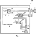
- Fig. 1 is a configuration diagram of a control device according to one embodiment of the present invention.
- a control device 100 includes a casing 1 and a control circuit substrate 2 arranged inside the casing 1.
- the control device 100 is a robot controller.
- the robot controller controls a drive voltage of a motor of a robot based on an input signal supplied from a difference device.
- a current corresponding to a driving amount of the motor is supplied to each phase of the motor (not shown).
- the control circuit substrate 2 includes a control circuit 3, a differential transceiver 5, termination resistors 6, relay circuits 7, an internal connector 4a, and an external connector 4b.
- the control circuit 3 generates a control signal (PWM signal) for controlling an output voltage of the motor driver based on a rotational position of the motor.
- the control circuit 3 then outputs the control signal (PWM signal) to the motor driver.
- the motor driver converts the output voltage of a power supply circuit into a multiphase AC voltage and outputs the multiphase AC voltage to the motor.
- the power supply circuit converts the AC voltage into a DC voltage and outputs the DC voltage to the motor driver.
- the control circuit 3 may be mounted on a circuit substrate different from a circuit substrate on which the motor driver and/or the power supply circuit is mounted, or the control circuit 3 may be mounted on the same circuit substrate as the motor driver and/or the power supply circuit.
- control circuit 3 has an expansion function for controlling input and output of various sensors in robot control.
- the control circuit 3 is connected to the internal connector 4a and the external connector 4b in parallel through the differential transceiver 5 and signal wires (LI, L2).
- the control circuit 3 is a master CPU mounted on a master board.
- the control circuit 3 is configured to perform differential serial transmission of half-duplex communication with a slave CPU (expansion circuit), mounted on a slave board (expansion circuit substrate), at an inside and outside of the casing 1 by the differential transceiver 5.
- the control circuit substrate, the control circuit, the expansion circuit substrate, and the expansion circuit may be referred to as a slave board, a master CPU, a slave board, and a slave CPU, respectively.
- the internal connector 4a is connected to a communication cable 10 in the casing 1.
- the internal connector 4a includes: signal terminals (1, 2) connected to the respective signal wires (LI, L2); a first terminal (3) connected to one of input terminals of the relay circuit 7; and a second terminal (4) connected to the other of the input terminals of the relay circuit 7.
- the internal connector 4a is connected to a cable connector 11 of the communication cable 10 inside the casing 1, the cable connector 11 being located close to the control circuit substrate 2.
- the external connector 4b is connected to the communication cable 10 outside the casing 1.
- the external connector 4b includes: signal terminals (1, 2) connected to the respective signal wires (LI, L2); a first terminal (3) connected to one of input terminals of the relay circuit 7; and a second terminal (4) connected to the other of the input terminals of the relay circuit 7.
- the external connector 4b is connected to a cable connector 11 of the communication cable 10 outside the casing 1, the cable connector 11 being located close to the control circuit substrate 2.
- the internal connector 4a and the external connector 4b may be collectively called a connector (specific connector) 4.
- the connector (hereinafter may be referred to as a "cable connector") 11 of the communication cable 10 includes: signal terminals (1, 2) connected to the respective signal terminals (1, 2) of the connector 4; and two short circuit terminals (3, 4) that are short-circuited in the connector 11.
- Each of the termination resistors 6 is arranged between a pair of signal wires (LI, L2).
- two termination resistors 6 are mounted on the control circuit substrate 2.
- One of the termination resistors 6 terminates the signal wires (LI, L2) connected to the internal connector 4a, and the other of the termination resistors 6 terminates the signal wires (LI, L2) connected to the external connector 4b.
- Each of the relay circuits 7 switches the termination resistor 6 between effective and ineffective.
- two relay circuits 7 are mounted on the control circuit substrate 2.
- One of the relay circuits 7 switches the termination resistor 6 connected to the internal connector 4a between effective and ineffective, and the other of the relay circuits 7 switches the termination resistor 6 connected to the external connector 4b between effective and ineffective.
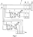
- the specific configurations of the relay circuits 7 will be described with reference to Fig. 2 . Since these two relay circuits 7 are the same in configuration as each other, only one relay circuit 7 will be described herein.
- the relay circuit 7 of the present embodiment is a photo MOS relay.
- the photo MOS relay is constituted by: a light emitting element (LED) as an input side; and a MOSFET and a light receiving element as output sides.
- an anode-side input terminal 71 is connected to a DC voltage supply terminal VCC through a resistor R, and a cathode-side input terminal 72 is connected to a ground terminal.
- an output terminal 73 is connected to the signal line L1 through the termination resistor 6, and an output terminal 74 is connected to the signal line L2.
- the connector 4 and the cable connector 11 are in a disconnected state.
- the internal connector 4a and the cable connector 11 are in the disconnected state.
- the first terminal (3) and the second terminal (4) in the internal connector 4a are not short-circuited, and a forward voltage is supplied to the input-side light emitting element (LED) of the relay circuit 7.
- LED input-side light emitting element
- the relay circuit 7 becomes an ON state.
- the output-side light receiving element receives the light of the LED, and the MOSFET conducts electricity.
- An output current flows between the output terminals (73, 74).
- the termination resistor 6 becomes effective.
- the connector 4 and the cable connector 11 are in a connected state.
- the external connector 4b and the cable connector 11 are in the connected state.
- the first terminal (3) and the second terminal (4) in the external connector 4b are short-circuited through the short circuit terminals (3, 4) of the cable connector 11, and the forward voltage is not supplied to the input-side light emitting element (LED). Therefore, the LED does not emit light, and the input current does not flow between the input terminals (71, 72).
- the relay circuit 7 is switched to an OFF state. When the relay circuit 7 is in the OFF state, the output-side light receiving element does not receive the light of the LED, and therefore, the MOSFET does not conduct electricity. The output current does not flow between the output terminals (73, 74). As a result, the termination resistor 6 becomes ineffective.
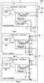
- a network connected to the control device 100 will be described with reference to Fig. 3 .
- four slave boards 20-1, 20-2, 20-3, and 20-4 are connected to a master board (2) of the control device 100.
- the slave boards 20-1 to 20-4 may be collectively called a slave board 20.
- the two slave boards 20-1 and 20-2 are daisy-chained to the internal connector 4a of the master board (2) through the communication cables 10.
- the two slave boards 20-3 and 20-4 are daisy-chained to the external connector 4b of the master board (2) through the communication cables 10.
- Fig. 4 is a diagram showing components inside the control device 100. As shown in Fig. 4 , inside the casing 1 of the control device 100, the internal connector 4a of the master board (2) is connected to the cable connector 11 of the communication cable 10 connected to the slave board 20-1.
- the relay circuit 7 connected to the internal connector 4a is in the OFF state, and the termination resistor 6 connected to the internal connector 4a becomes ineffective.
- the relay circuit 7 connected to the external connector 4b is also in the OFF state, and the termination resistor 6 connected to the external connector 4b also becomes ineffective.
- the slave board 20-1 includes a slave CPU 30, the differential transceiver 5, the termination resistor 6, the relay circuit 7, a first connector 40a, and a second connector 40b. It should be noted that since the configurations of the differential transceiver 5, the termination resistor 6, and the relay circuit 7 are the same as the above-described configurations, explanations thereof are omitted. Since the four slave boards 20-1 to 20-4 are the same in configuration as each other, only the slave board 20-1 will be described herein.
- the first connector 40a of the slave board 20-1 is in connection with the cable connector 11 of the communication cable 10 connected to the internal connector 4a of the master board (2), and the second connector 40b of the slave board 20-1 is in connection with the cable connector 11 of the communication cable 10 connected to the first connector 40a of the slave board 20-2.
- the relay circuit 7 of the slave board 20-1 becomes the OFF state, and the termination resistor 6 of the slave board 20-1 becomes ineffective.
- the first connector 40a of the slave board 20-2 is in connection with the cable connector 11 of the communication cable 10 connected to the second connector 40b of the slave board 20-1, and the second connector 40b of the slave board 20-2 is in a disconnected state. With this, the relay circuit 7 of the slave board 20-2 becomes the ON state, and the termination resistor 6 becomes effective.
- Fig. 5 is a diagram showing components outside the control device 100.
- the first connector 40a of the slave board 20-3 is in connection with the cable connector 11 of the communication cable 10 connected to the external connector 4b of the master board (2)
- the second connector 40b of the slave board 20-3 is in connection with the cable connector 11 of the communication cable 10 connected to the first connector 40a of the slave board 20-4.
- the relay circuit 7 of the slave board 20-3 becomes the OFF state, and the termination resistor 6 becomes ineffective.
- the first connector 40a of the slave board 20-4 is in connection with the cable connector 11 of the communication cable 10 connected to the second connector 40b of the slave board 20-3, and the second connector 40b of the slave board 20-4 is in a disconnected state. With this, the relay circuit 7 of the slave board 20-4 becomes the ON state, and the termination resistor 6 of the slave board 20-4 becomes effective.
- the master board (2) includes the connectors 4 that are connectable to the slave board 20 and provided inside and outside the casing 1. Therefore, the slave boards 20 can be daisy-chained to the master board (2) not only inside the casing 1 but also outside the casing 1. Further, the relay circuits 7 are included on the master board (2). Therefore, regardless of the inside and outside of the casing 1, the termination resistor 6 can switch between ineffective and effective by connection/disconnection between the connector 4 and the cable connector 11.
- the master board (2) is connected through the communication cables 10 to the two slave boards 20-1 and 20-2, and outside the casing 1, the master board (2) is connected through the communication cables 10 to the two slave boards 20-3 and 20-4 accommodated in respective external devices 200. Since the two slave boards 20-1 and 20-2 are connected to each other through the communication cable 10, flexible substrate arrangement can be realized inside the casing 1. Herein, since the slave boards 20-1 and 20-2 are arranged parallel to the master board (2), this can contribute to the downsizing of the control device 100.
- two slave boards 20 are included inside the casing 1 (see Fig. 6 ). However, three or more slave boards 20 may be included inside the casing 1.
- the relay circuit 7 is constituted by the photo MOS relay (see Fig. 2 ).
- the relay circuit 7 may be constituted by a different circuit (mechanical relay, for example) as long as the circuit has the above function of switching the termination resistor 6 between effective and ineffective.
- the present invention is useful for control devices, such as robot controllers.
Landscapes
- Engineering & Computer Science (AREA)
- Microelectronics & Electronic Packaging (AREA)
- Robotics (AREA)
- Mechanical Engineering (AREA)
- Signal Processing (AREA)
- Power Engineering (AREA)
- Computer Networks & Wireless Communication (AREA)
- General Physics & Mathematics (AREA)
- Automation & Control Theory (AREA)
- Physics & Mathematics (AREA)
- Manipulator (AREA)
- Programmable Controllers (AREA)
- Structure Of Telephone Exchanges (AREA)
Abstract
Description
- The present invention relates to a control device, such as a robot controller.
- In recent years, there is an increasing need for high expandability and downsizing of control devices that support social infrastructure/public system products and the like. For example,
PTL 1 discloses a control device including a casing in which a plurality of expansion I/O boards can be arranged. - PTL 1: Japanese Laid-Open Patent Application Publication No.
2012-256768 - However, since the conventional control device is configured such that the expansion I/O boards are arranged inside the casing, an adequate space needs to be secured inside the casing. As a result, increases in size and weight of the device are unavoidable, and expansion work performed by a user becomes complex. Such problems are common among control devices, such as robot controllers, having high expandability.
- The present invention was made to solve the above problems, and an object of the present invention is to facilitate the expansion work of a user while realizing downsizing of a control device, such as a robot controller, having high expandability.
- To achieve the above object, a control device according to one aspect of the present invention includes: a casing; and a control circuit substrate arranged inside the casing, wherein: the control circuit substrate includes a control circuit mounted on the control circuit substrate, an internal connector connectable to a communication cable inside the casing, the communication cable being connected to an expansion circuit substrate, and an external connector connectable to another communication cable outside the casing, the another communication cable being connected to another expansion circuit substrate; and the control circuit is connected to the internal connector and the external connector in parallel.
- According to the above configuration, the control circuit substrate includes the connectors that are connectable to the expansion circuit substrate and provided inside and outside the casing. Therefore, the expansion circuit substrate can be connected to the control circuit substrate not only inside the casing but also outside the casing. Thus, expansion work performed by a user is facilitated. This can contribute to the downsizing of the control device as compared to a conventional configuration in which the expansion circuit substrate is arranged only inside the casing.
- The control circuit substrate may further include a termination resistor arranged between a pair of signal wires, and a relay circuit configured to switch the termination resistor between effective and ineffective. At least one of the internal connector and the external connector may be defined as a specific connector, and each of connectors of the communication cables connected to the respective expansion circuit substrates may be defined as a cable connector, the connector being located close to the control circuit substrate. One of output terminals of the relay circuit may be connected to the termination resistor, and the other of the output terminals of the relay circuit may be connected to one of the signal wires. When the specific connector and the cable connector are in a disconnected state, the relay circuit may be in an ON state, and an output current may flow, and this may make the termination resistor effective. When the specific connector and the cable connector are in a connected state, the relay circuit may be switched to an OFF state, and the output current may stop, and this may make the termination resistor ineffective.
- According to the above configuration, the control circuit substrate includes the relay circuit configured to switch the termination resistor between effective and ineffective. Therefore, regardless of the inside and outside of the casing, the termination resistor that terminates a pair of signal wires can switch between ineffective and effective by connection/disconnection between the connector and the cable connector. On this account, work of attaching the termination resistor and switching the termination resistor becomes unnecessary in the expansion work of the substrate. Thus, the expansion work performed by a user is facilitated.
- The specific connector may include signal terminals connected to the respective signal wires, a first terminal connected to one of input terminals of the relay circuit, and a second terminal connected to the other of the input terminals of the relay circuit. The cable connector may include signal terminals connected to the respective signal terminals of the specific connector, and two short circuit terminals that are short-circuited inside the cable connector. The one input terminal of the relay circuit may be connected to a DC voltage supply terminal. The other input terminal of the relay circuit may be connected to a ground terminal. When the specific connector and the cable connector are in a disconnected state, an input current may flow between the input terminals of the relay circuit, and the relay circuit may be in an ON state. When the specific connector and the cable connector are in a connected state, the first terminal and the second terminal may be short-circuited through the short circuit terminals, and the relay circuit may be switched to an OFF state.
- Inside the casing, the control circuit substrate may be connectable to at least the two expansion circuit substrates through the communication cables and be arranged parallel to these expansion circuit substrates.
- According to the above configuration, even when, for example, two expansion circuit substrates are arranged inside the casing, the two expansion circuit substrates can be connected to each other through the communication cable, and therefore, flexible substrate arrangement can be realized. When these expansion circuit substrates are arranged parallel to the control circuit substrate, this can contribute to the downsizing of the control device.
- The control device of the present invention is configured as described above and can facilitate expansion work of a user while realizing downsizing of a control device, such as a robot controller, having high expandability.
-
-
Fig. 1 is a configuration diagram of a control device according to one embodiment of the present invention. -
Fig. 2 is a circuit diagram showing the configurations of relay circuits shown inFig. 1 . -
Fig. 3 is a diagram showing one example of the configuration of a network of the control device shown inFig. 1 . -
Fig. 4 is a diagram showing components inside the control device shown inFig. 3 . -
Fig. 5 is a diagram showing components outside the control device shown inFig. 3 . -
Fig. 6 is a perspective view schematically showing an appearance of the control device shown inFig. 3 . - Hereinafter, a preferred embodiment will be described with reference to the drawings. In the following description and the drawings, the same reference signs are used for the same or corresponding components, and a repetition of the same explanation is avoided. For ease of understanding, components are schematically shown in the drawings.
-
Fig. 1 is a configuration diagram of a control device according to one embodiment of the present invention. As shown inFig. 1 , acontrol device 100 includes acasing 1 and acontrol circuit substrate 2 arranged inside thecasing 1. In the present embodiment, thecontrol device 100 is a robot controller. The robot controller controls a drive voltage of a motor of a robot based on an input signal supplied from a difference device. When the robot controller controls a frequency of a control signal input to a motor driver, a current corresponding to a driving amount of the motor is supplied to each phase of the motor (not shown). - The
control circuit substrate 2 includes acontrol circuit 3, adifferential transceiver 5,termination resistors 6,relay circuits 7, aninternal connector 4a, and anexternal connector 4b. - The
control circuit 3 generates a control signal (PWM signal) for controlling an output voltage of the motor driver based on a rotational position of the motor. Thecontrol circuit 3 then outputs the control signal (PWM signal) to the motor driver. The motor driver converts the output voltage of a power supply circuit into a multiphase AC voltage and outputs the multiphase AC voltage to the motor. The power supply circuit converts the AC voltage into a DC voltage and outputs the DC voltage to the motor driver. Thecontrol circuit 3 may be mounted on a circuit substrate different from a circuit substrate on which the motor driver and/or the power supply circuit is mounted, or thecontrol circuit 3 may be mounted on the same circuit substrate as the motor driver and/or the power supply circuit. - In addition to the above function of controlling the robot, the
control circuit 3 has an expansion function for controlling input and output of various sensors in robot control. In the present embodiment, thecontrol circuit 3 is connected to theinternal connector 4a and theexternal connector 4b in parallel through thedifferential transceiver 5 and signal wires (LI, L2). Thecontrol circuit 3 is a master CPU mounted on a master board. Thecontrol circuit 3 is configured to perform differential serial transmission of half-duplex communication with a slave CPU (expansion circuit), mounted on a slave board (expansion circuit substrate), at an inside and outside of thecasing 1 by thedifferential transceiver 5. Hereinafter, the control circuit substrate, the control circuit, the expansion circuit substrate, and the expansion circuit may be referred to as a slave board, a master CPU, a slave board, and a slave CPU, respectively. - The
internal connector 4a is connected to acommunication cable 10 in thecasing 1. Theinternal connector 4a includes: signal terminals (1, 2) connected to the respective signal wires (LI, L2); a first terminal (3) connected to one of input terminals of therelay circuit 7; and a second terminal (4) connected to the other of the input terminals of therelay circuit 7. Theinternal connector 4a is connected to acable connector 11 of thecommunication cable 10 inside thecasing 1, thecable connector 11 being located close to thecontrol circuit substrate 2. - The
external connector 4b is connected to thecommunication cable 10 outside thecasing 1. Theexternal connector 4b includes: signal terminals (1, 2) connected to the respective signal wires (LI, L2); a first terminal (3) connected to one of input terminals of therelay circuit 7; and a second terminal (4) connected to the other of the input terminals of therelay circuit 7. Theexternal connector 4b is connected to acable connector 11 of thecommunication cable 10 outside thecasing 1, thecable connector 11 being located close to thecontrol circuit substrate 2. Hereinafter, theinternal connector 4a and theexternal connector 4b may be collectively called a connector (specific connector) 4. - The connector (hereinafter may be referred to as a "cable connector") 11 of the
communication cable 10 includes: signal terminals (1, 2) connected to the respective signal terminals (1, 2) of theconnector 4; and two short circuit terminals (3, 4) that are short-circuited in theconnector 11. - Each of the
termination resistors 6 is arranged between a pair of signal wires (LI, L2). In the present embodiment, twotermination resistors 6 are mounted on thecontrol circuit substrate 2. One of thetermination resistors 6 terminates the signal wires (LI, L2) connected to theinternal connector 4a, and the other of thetermination resistors 6 terminates the signal wires (LI, L2) connected to theexternal connector 4b. - Each of the
relay circuits 7 switches thetermination resistor 6 between effective and ineffective. In the present embodiment, tworelay circuits 7 are mounted on thecontrol circuit substrate 2. One of therelay circuits 7 switches thetermination resistor 6 connected to theinternal connector 4a between effective and ineffective, and the other of therelay circuits 7 switches thetermination resistor 6 connected to theexternal connector 4b between effective and ineffective. Next, the specific configurations of therelay circuits 7 will be described with reference toFig. 2 . Since these tworelay circuits 7 are the same in configuration as each other, only onerelay circuit 7 will be described herein. - As shown in
Fig. 2 , therelay circuit 7 of the present embodiment is a photo MOS relay. The photo MOS relay is constituted by: a light emitting element (LED) as an input side; and a MOSFET and a light receiving element as output sides. In therelay circuit 7, an anode-side input terminal 71 is connected to a DC voltage supply terminal VCC through a resistor R, and a cathode-side input terminal 72 is connected to a ground terminal. In therelay circuit 7, anoutput terminal 73 is connected to the signal line L1 through thetermination resistor 6, and anoutput terminal 74 is connected to the signal line L2. - The following will describe a case where the
connector 4 and thecable connector 11 are in a disconnected state. As shown inFig. 2 , theinternal connector 4a and thecable connector 11 are in the disconnected state. The first terminal (3) and the second terminal (4) in theinternal connector 4a are not short-circuited, and a forward voltage is supplied to the input-side light emitting element (LED) of therelay circuit 7. With this, the LED emits light, and an input current flows between the input terminals (71, 72). Therelay circuit 7 becomes an ON state. When therelay circuit 7 is in the ON state, the output-side light receiving element receives the light of the LED, and the MOSFET conducts electricity. An output current flows between the output terminals (73, 74). As a result, thetermination resistor 6 becomes effective. - Next, the following will describe a case where the
connector 4 and thecable connector 11 are in a connected state. As shown inFig. 2 , theexternal connector 4b and thecable connector 11 are in the connected state. The first terminal (3) and the second terminal (4) in theexternal connector 4b are short-circuited through the short circuit terminals (3, 4) of thecable connector 11, and the forward voltage is not supplied to the input-side light emitting element (LED). Therefore, the LED does not emit light, and the input current does not flow between the input terminals (71, 72). Therelay circuit 7 is switched to an OFF state. When therelay circuit 7 is in the OFF state, the output-side light receiving element does not receive the light of the LED, and therefore, the MOSFET does not conduct electricity. The output current does not flow between the output terminals (73, 74). As a result, thetermination resistor 6 becomes ineffective. - Next, the configuration of a network connected to the
control device 100 will be described with reference toFig. 3 . As shown inFig. 3 , four slave boards 20-1, 20-2, 20-3, and 20-4 are connected to a master board (2) of thecontrol device 100. Hereinafter, the slave boards 20-1 to 20-4 may be collectively called a slave board 20. Inside thecasing 1 of thecontrol device 100, the two slave boards 20-1 and 20-2 are daisy-chained to theinternal connector 4a of the master board (2) through thecommunication cables 10. Outside thecasing 1 of thecontrol device 100, the two slave boards 20-3 and 20-4 are daisy-chained to theexternal connector 4b of the master board (2) through thecommunication cables 10. -
Fig. 4 is a diagram showing components inside thecontrol device 100. As shown inFig. 4 , inside thecasing 1 of thecontrol device 100, theinternal connector 4a of the master board (2) is connected to thecable connector 11 of thecommunication cable 10 connected to the slave board 20-1. - Since the
internal connector 4a of the master board (2) and thecable connector 11 are in the connected state, therelay circuit 7 connected to theinternal connector 4a is in the OFF state, and thetermination resistor 6 connected to theinternal connector 4a becomes ineffective. On the other hand, since theexternal connector 4b of the master board (2) and thecable connector 11 are also in the connected state, therelay circuit 7 connected to theexternal connector 4b is also in the OFF state, and thetermination resistor 6 connected to theexternal connector 4b also becomes ineffective. - The slave board 20-1 includes a
slave CPU 30, thedifferential transceiver 5, thetermination resistor 6, therelay circuit 7, afirst connector 40a, and asecond connector 40b. It should be noted that since the configurations of thedifferential transceiver 5, thetermination resistor 6, and therelay circuit 7 are the same as the above-described configurations, explanations thereof are omitted. Since the four slave boards 20-1 to 20-4 are the same in configuration as each other, only the slave board 20-1 will be described herein. - The
first connector 40a of the slave board 20-1 is in connection with thecable connector 11 of thecommunication cable 10 connected to theinternal connector 4a of the master board (2), and thesecond connector 40b of the slave board 20-1 is in connection with thecable connector 11 of thecommunication cable 10 connected to thefirst connector 40a of the slave board 20-2. With this, therelay circuit 7 of the slave board 20-1 becomes the OFF state, and thetermination resistor 6 of the slave board 20-1 becomes ineffective. - The
first connector 40a of the slave board 20-2 is in connection with thecable connector 11 of thecommunication cable 10 connected to thesecond connector 40b of the slave board 20-1, and thesecond connector 40b of the slave board 20-2 is in a disconnected state. With this, therelay circuit 7 of the slave board 20-2 becomes the ON state, and thetermination resistor 6 becomes effective. -
Fig. 5 is a diagram showing components outside thecontrol device 100. As shown inFig. 5 , outside thecasing 1 of thecontrol device 100, thefirst connector 40a of the slave board 20-3 is in connection with thecable connector 11 of thecommunication cable 10 connected to theexternal connector 4b of the master board (2), and thesecond connector 40b of the slave board 20-3 is in connection with thecable connector 11 of thecommunication cable 10 connected to thefirst connector 40a of the slave board 20-4. With this, therelay circuit 7 of the slave board 20-3 becomes the OFF state, and thetermination resistor 6 becomes ineffective. - The
first connector 40a of the slave board 20-4 is in connection with thecable connector 11 of thecommunication cable 10 connected to thesecond connector 40b of the slave board 20-3, and thesecond connector 40b of the slave board 20-4 is in a disconnected state. With this, therelay circuit 7 of the slave board 20-4 becomes the ON state, and thetermination resistor 6 of the slave board 20-4 becomes effective. - Therefore, according to the present embodiment, the master board (2) includes the
connectors 4 that are connectable to the slave board 20 and provided inside and outside thecasing 1. Therefore, the slave boards 20 can be daisy-chained to the master board (2) not only inside thecasing 1 but also outside thecasing 1. Further, therelay circuits 7 are included on the master board (2). Therefore, regardless of the inside and outside of thecasing 1, thetermination resistor 6 can switch between ineffective and effective by connection/disconnection between theconnector 4 and thecable connector 11. - Conventionally, a plurality of (four, for example) slave boards 20 are accommodated inside the
casing 1 of thecontrol device 100. Therefore, an adequate space needs to be secured inside thecasing 1. On this account, increases in size and weight of the apparatus are unavoidable, and expansion work performed by a user becomes complex. - However, according to the
control device 100 of the present embodiment, as shown inFig. 6 , inside thecasing 1, the master board (2) is connected through thecommunication cables 10 to the two slave boards 20-1 and 20-2, and outside thecasing 1, the master board (2) is connected through thecommunication cables 10 to the two slave boards 20-3 and 20-4 accommodated in respectiveexternal devices 200. Since the two slave boards 20-1 and 20-2 are connected to each other through thecommunication cable 10, flexible substrate arrangement can be realized inside thecasing 1. Herein, since the slave boards 20-1 and 20-2 are arranged parallel to the master board (2), this can contribute to the downsizing of thecontrol device 100. - In the present embodiment, two slave boards 20 are included inside the casing 1 (see
Fig. 6 ). However, three or more slave boards 20 may be included inside thecasing 1. - In the present embodiment, the
relay circuit 7 is constituted by the photo MOS relay (seeFig. 2 ). However, therelay circuit 7 may be constituted by a different circuit (mechanical relay, for example) as long as the circuit has the above function of switching thetermination resistor 6 between effective and ineffective. - From the foregoing explanation, many modifications and other embodiments of the present invention are obvious to one skilled in the art. Therefore, the foregoing explanation should be interpreted only as an example and is provided for the purpose of teaching the best mode for carrying out the present invention to one skilled in the art. The structures and/or functional details may be substantially modified within the scope of the present invention.
- The present invention is useful for control devices, such as robot controllers.
-
- 1
- casing
- 2
- control circuit substrate (master board)
- 3
- master CPU (control circuit)
- 4
- connector (master CPU)
- 4a
- internal connector
- 4b
- external connector
- 5
- differential transceiver
- 6
- termination resistor
- 7
- relay circuit
- 10
- communication cable
- 11
- cable connector
- 20, 20-1 to 20-4
- slave board (expansion circuit substrate)
- 30
- slave CPU
- 100
- control device (robot controller)
- 200
- external device
Claims (4)
- A control device comprising:a casing; anda control circuit substrate arranged inside the casing, wherein:the control circuit substrate includesa control circuit mounted on the control circuit substrate,an internal connector connectable to a communication cable inside the casing, the communication cable being connected to an expansion circuit substrate, andan external connector connectable to another communication cable outside the casing, the another communication cable being connected to another expansion circuit substrate; andthe control circuit is connected to the internal connector and the external connector in parallel.
- The control device according to claim 1, wherein:the control circuit substrate further includesa termination resistor arranged between a pair of signal wires, anda relay circuit configured to switch the termination resistor between effective and ineffective;at least one of the internal connector and the external connector is defined as a specific connector;each of connectors of the communication cables connected to the respective expansion circuit substrates is defined as a cable connector, the connector being located close to the control circuit substrate;one of output terminals of the relay circuit is connected to the termination resistor;the other of the output terminals of the relay circuit is connected to one of the signal wires;when the specific connector and the cable connector are in a disconnected state, the relay circuit is in an ON state, and an output current flows, and this makes the termination resistor effective; andwhen the specific connector and the cable connector are in a connected state, the relay circuit is switched to an OFF state, and the output current stops, and this makes the termination resistor ineffective.
- The control device according to claim 2, wherein:the specific connector includessignal terminals connected to the respective signal wires,a first terminal connected to one of input terminals of the relay circuit, anda second terminal connected to the other of the input terminals of the relay circuit;the cable connector includessignal terminals connected to the respective signal terminals of the specific connector, andtwo short circuit terminals that are short-circuited inside the cable connector;the one input terminal of the relay circuit is connected to a DC voltage supply terminal;the other input terminal of the relay circuit is connected to a ground terminal;when the specific connector and the cable connector are in a disconnected state, an input current flows between the input terminals of the relay circuit, and the relay circuit is in an ON state; andwhen the specific connector and the cable connector are in a connected state, the first terminal and the second terminal are short-circuited through the short circuit terminals, and the relay circuit is switched to an OFF state.
- The control device according to any one of claims 1 to 3, wherein inside the casing, the control circuit substrate is connectable to at least the two expansion circuit substrates through the communication cables and is arranged parallel to these expansion circuit substrates.
Applications Claiming Priority (2)
| Application Number | Priority Date | Filing Date | Title |
|---|---|---|---|
| JP2017034989A JP6803262B2 (en) | 2017-02-27 | 2017-02-27 | Control device |
| PCT/JP2018/007261 WO2018155708A1 (en) | 2017-02-27 | 2018-02-27 | Control device |
Publications (3)
| Publication Number | Publication Date |
|---|---|
| EP3588213A1 true EP3588213A1 (en) | 2020-01-01 |
| EP3588213A4 EP3588213A4 (en) | 2020-12-30 |
| EP3588213B1 EP3588213B1 (en) | 2023-06-21 |
Family
ID=63252882
Family Applications (1)
| Application Number | Title | Priority Date | Filing Date |
|---|---|---|---|
| EP18757834.9A Active EP3588213B1 (en) | 2017-02-27 | 2018-02-27 | Control device |
Country Status (6)
| Country | Link |
|---|---|
| US (1) | US11277931B2 (en) |
| EP (1) | EP3588213B1 (en) |
| JP (1) | JP6803262B2 (en) |
| KR (1) | KR102263838B1 (en) |
| CN (1) | CN110366708B (en) |
| WO (1) | WO2018155708A1 (en) |
Families Citing this family (5)
| Publication number | Priority date | Publication date | Assignee | Title |
|---|---|---|---|---|
| KR102338115B1 (en) | 2020-02-28 | 2021-12-10 | 엘에스일렉트릭 (주) | Connector and communication system |
| JP7415824B2 (en) * | 2020-06-30 | 2024-01-17 | 横河電機株式会社 | Expansion module, CPU module, system, and communication method |
| JP7559073B2 (en) | 2020-09-03 | 2024-10-01 | 川崎重工業株式会社 | Substrate Transport Robot System |
| CN115114149A (en) * | 2022-06-17 | 2022-09-27 | 中国第一汽车股份有限公司 | JTAG interface, and debugging method and device of JTAG interface |
| CN117621139A (en) * | 2022-08-09 | 2024-03-01 | 深圳忆海原识科技有限公司 | A modular assembled drive circuit module |
Family Cites Families (19)
| Publication number | Priority date | Publication date | Assignee | Title |
|---|---|---|---|---|
| US4604689A (en) * | 1983-04-15 | 1986-08-05 | Convergent Technologies, Inc. | Bus repeater |
| JPS62155645A (en) * | 1984-12-17 | 1987-07-10 | Takeshi Nakano | Line converter |
| JPH0273444A (en) * | 1988-09-09 | 1990-03-13 | Canon Inc | computer equipment |
| JPH09325839A (en) * | 1996-06-06 | 1997-12-16 | Saitama Nippon Denki Kk | Termination method between devices |
| WO1999053627A1 (en) * | 1998-04-10 | 1999-10-21 | Chrimar Systems, Inc. Doing Business As Cms Technologies | System for communicating with electronic equipment on a network |
| US6978335B2 (en) * | 2000-06-30 | 2005-12-20 | 02Micro International Limited | Smart card virtual hub |
| US6237056B1 (en) * | 2000-07-14 | 2001-05-22 | Videon, Inc. | Apparatus and method for high speed board-to board ribbon cable data transfer |
| US20040015637A1 (en) * | 2002-07-22 | 2004-01-22 | Cedric Yau | Multiple bus interface for a computer system |
| US6896541B2 (en) * | 2003-02-18 | 2005-05-24 | Hewlett-Packard Development Company, L.P. | Interface connector that enables detection of cable connection |
| US7241218B2 (en) * | 2003-05-06 | 2007-07-10 | Ruskin Company | Fire/smoke damper control system |
| US8066515B2 (en) * | 2004-11-17 | 2011-11-29 | Nvidia Corporation | Multiple graphics adapter connection systems |
| US20110134792A1 (en) * | 2004-11-19 | 2011-06-09 | Jan Olof Andersson | Method and Apparatus for a Hub in Daisy Chain Configuration |
| JP4648166B2 (en) * | 2005-11-24 | 2011-03-09 | 新電元工業株式会社 | System power supply and power supply system |
| US7544077B1 (en) * | 2008-02-08 | 2009-06-09 | Tyco Electronics Corporation | Control device for a power distribution system |
| JP5098936B2 (en) * | 2008-04-15 | 2012-12-12 | 株式会社安川電機 | Servo control device |
| JP5473817B2 (en) * | 2010-07-23 | 2014-04-16 | 三菱電機株式会社 | Programmable controller and bus converter |
| JP5810584B2 (en) * | 2011-03-30 | 2015-11-11 | セイコーエプソン株式会社 | Robot controller |
| JP5637937B2 (en) | 2011-06-10 | 2014-12-10 | 株式会社日立製作所 | Control device |
| KR101104103B1 (en) * | 2011-11-08 | 2012-01-12 | 주식회사 비엠티 | Modular Safety Booth Bars |
-
2017
- 2017-02-27 JP JP2017034989A patent/JP6803262B2/en active Active
-
2018
- 2018-02-27 CN CN201880014204.7A patent/CN110366708B/en active Active
- 2018-02-27 EP EP18757834.9A patent/EP3588213B1/en active Active
- 2018-02-27 KR KR1020197026465A patent/KR102263838B1/en active Active
- 2018-02-27 US US16/489,304 patent/US11277931B2/en active Active
- 2018-02-27 WO PCT/JP2018/007261 patent/WO2018155708A1/en not_active Ceased
Also Published As
| Publication number | Publication date |
|---|---|
| EP3588213A4 (en) | 2020-12-30 |
| JP6803262B2 (en) | 2020-12-23 |
| WO2018155708A1 (en) | 2018-08-30 |
| CN110366708B (en) | 2022-03-04 |
| KR102263838B1 (en) | 2021-06-14 |
| US11277931B2 (en) | 2022-03-15 |
| US20200068739A1 (en) | 2020-02-27 |
| KR20190117611A (en) | 2019-10-16 |
| EP3588213B1 (en) | 2023-06-21 |
| CN110366708A (en) | 2019-10-22 |
| JP2018142100A (en) | 2018-09-13 |
Similar Documents
| Publication | Publication Date | Title |
|---|---|---|
| US11277931B2 (en) | Control device | |
| US12004282B2 (en) | Hybrid dimming controller with multi-class outputs | |
| CA2831436C (en) | Converter assembly, method for producing a converter assembly and method for operating a converter assembly | |
| US9966881B2 (en) | Bluetooth motor controller, brushless direct current motor, and multi-motor system comprising the same | |
| WO2013130432A1 (en) | Connector having wireless control capabilities | |
| US9621379B2 (en) | Arrangement for connecting a component to a master controller in a motor vehicle | |
| US11749485B2 (en) | Modular switch apparatus for controlling at least one electric drive | |
| US9385494B2 (en) | Power extending board and power supply system using same | |
| JP6591083B2 (en) | controller | |
| US10831695B2 (en) | Communication system | |
| EP4094420B1 (en) | Building technology device | |
| CN106602967B (en) | Integrated motor drive unit structure | |
| US20070115136A1 (en) | Contact signal transmission and reception apparatus | |
| CN110401115B (en) | Back sheet and method for manufacturing same | |
| CN210402685U (en) | Master-slave intelligent electric appliance control system | |
| JP7110717B2 (en) | relay controller | |
| ES2702104T3 (en) | Electromotive drive system | |
| WO2018061073A1 (en) | Controller and driver unit | |
| JP2022163032A (en) | Relay control device | |
| JP2001337727A (en) | Multiple power supply connection device |
Legal Events
| Date | Code | Title | Description |
|---|---|---|---|
| STAA | Information on the status of an ep patent application or granted ep patent |
Free format text: STATUS: THE INTERNATIONAL PUBLICATION HAS BEEN MADE |
|
| PUAI | Public reference made under article 153(3) epc to a published international application that has entered the european phase |
Free format text: ORIGINAL CODE: 0009012 |
|
| STAA | Information on the status of an ep patent application or granted ep patent |
Free format text: STATUS: REQUEST FOR EXAMINATION WAS MADE |
|
| 17P | Request for examination filed |
Effective date: 20190827 |
|
| AK | Designated contracting states |
Kind code of ref document: A1 Designated state(s): AL AT BE BG CH CY CZ DE DK EE ES FI FR GB GR HR HU IE IS IT LI LT LU LV MC MK MT NL NO PL PT RO RS SE SI SK SM TR |
|
| AX | Request for extension of the european patent |
Extension state: BA ME |
|
| DAV | Request for validation of the european patent (deleted) | ||
| DAX | Request for extension of the european patent (deleted) | ||
| A4 | Supplementary search report drawn up and despatched |
Effective date: 20201201 |
|
| RIC1 | Information provided on ipc code assigned before grant |
Ipc: G05B 19/05 20060101ALN20201125BHEP Ipc: H04L 25/02 20060101ALI20201125BHEP Ipc: G05B 19/042 20060101AFI20201125BHEP Ipc: B25J 19/00 20060101ALI20201125BHEP |
|
| STAA | Information on the status of an ep patent application or granted ep patent |
Free format text: STATUS: EXAMINATION IS IN PROGRESS |
|
| 17Q | First examination report despatched |
Effective date: 20220429 |
|
| RIC1 | Information provided on ipc code assigned before grant |
Ipc: G05B 19/05 20060101ALN20221122BHEP Ipc: H04L 25/02 20060101ALI20221122BHEP Ipc: B25J 19/00 20060101ALI20221122BHEP Ipc: G05B 19/042 20060101AFI20221122BHEP |
|
| GRAP | Despatch of communication of intention to grant a patent |
Free format text: ORIGINAL CODE: EPIDOSNIGR1 |
|
| STAA | Information on the status of an ep patent application or granted ep patent |
Free format text: STATUS: GRANT OF PATENT IS INTENDED |
|
| RIC1 | Information provided on ipc code assigned before grant |
Ipc: G05B 19/05 20060101ALN20221207BHEP Ipc: H04L 25/02 20060101ALI20221207BHEP Ipc: B25J 19/00 20060101ALI20221207BHEP Ipc: G05B 19/042 20060101AFI20221207BHEP |
|
| INTG | Intention to grant announced |
Effective date: 20230103 |
|
| GRAS | Grant fee paid |
Free format text: ORIGINAL CODE: EPIDOSNIGR3 |
|
| GRAA | (expected) grant |
Free format text: ORIGINAL CODE: 0009210 |
|
| STAA | Information on the status of an ep patent application or granted ep patent |
Free format text: STATUS: THE PATENT HAS BEEN GRANTED |
|
| AK | Designated contracting states |
Kind code of ref document: B1 Designated state(s): AL AT BE BG CH CY CZ DE DK EE ES FI FR GB GR HR HU IE IS IT LI LT LU LV MC MK MT NL NO PL PT RO RS SE SI SK SM TR |
|
| REG | Reference to a national code |
Ref country code: CH Ref legal event code: EP |
|
| REG | Reference to a national code |
Ref country code: DE Ref legal event code: R096 Ref document number: 602018052125 Country of ref document: DE |
|
| REG | Reference to a national code |
Ref country code: AT Ref legal event code: REF Ref document number: 1581341 Country of ref document: AT Kind code of ref document: T Effective date: 20230715 |
|
| REG | Reference to a national code |
Ref country code: IE Ref legal event code: FG4D |
|
| REG | Reference to a national code |
Ref country code: LT Ref legal event code: MG9D |
|
| REG | Reference to a national code |
Ref country code: NL Ref legal event code: MP Effective date: 20230621 |
|
| PG25 | Lapsed in a contracting state [announced via postgrant information from national office to epo] |
Ref country code: SE Free format text: LAPSE BECAUSE OF FAILURE TO SUBMIT A TRANSLATION OF THE DESCRIPTION OR TO PAY THE FEE WITHIN THE PRESCRIBED TIME-LIMIT Effective date: 20230621 Ref country code: NO Free format text: LAPSE BECAUSE OF FAILURE TO SUBMIT A TRANSLATION OF THE DESCRIPTION OR TO PAY THE FEE WITHIN THE PRESCRIBED TIME-LIMIT Effective date: 20230921 |
|
| REG | Reference to a national code |
Ref country code: AT Ref legal event code: MK05 Ref document number: 1581341 Country of ref document: AT Kind code of ref document: T Effective date: 20230621 |
|
| PG25 | Lapsed in a contracting state [announced via postgrant information from national office to epo] |
Ref country code: RS Free format text: LAPSE BECAUSE OF FAILURE TO SUBMIT A TRANSLATION OF THE DESCRIPTION OR TO PAY THE FEE WITHIN THE PRESCRIBED TIME-LIMIT Effective date: 20230621 Ref country code: NL Free format text: LAPSE BECAUSE OF FAILURE TO SUBMIT A TRANSLATION OF THE DESCRIPTION OR TO PAY THE FEE WITHIN THE PRESCRIBED TIME-LIMIT Effective date: 20230621 Ref country code: LV Free format text: LAPSE BECAUSE OF FAILURE TO SUBMIT A TRANSLATION OF THE DESCRIPTION OR TO PAY THE FEE WITHIN THE PRESCRIBED TIME-LIMIT Effective date: 20230621 Ref country code: LT Free format text: LAPSE BECAUSE OF FAILURE TO SUBMIT A TRANSLATION OF THE DESCRIPTION OR TO PAY THE FEE WITHIN THE PRESCRIBED TIME-LIMIT Effective date: 20230621 Ref country code: HR Free format text: LAPSE BECAUSE OF FAILURE TO SUBMIT A TRANSLATION OF THE DESCRIPTION OR TO PAY THE FEE WITHIN THE PRESCRIBED TIME-LIMIT Effective date: 20230621 Ref country code: GR Free format text: LAPSE BECAUSE OF FAILURE TO SUBMIT A TRANSLATION OF THE DESCRIPTION OR TO PAY THE FEE WITHIN THE PRESCRIBED TIME-LIMIT Effective date: 20230922 |
|
| PG25 | Lapsed in a contracting state [announced via postgrant information from national office to epo] |
Ref country code: FI Free format text: LAPSE BECAUSE OF FAILURE TO SUBMIT A TRANSLATION OF THE DESCRIPTION OR TO PAY THE FEE WITHIN THE PRESCRIBED TIME-LIMIT Effective date: 20230621 |
|
| PG25 | Lapsed in a contracting state [announced via postgrant information from national office to epo] |
Ref country code: SK Free format text: LAPSE BECAUSE OF FAILURE TO SUBMIT A TRANSLATION OF THE DESCRIPTION OR TO PAY THE FEE WITHIN THE PRESCRIBED TIME-LIMIT Effective date: 20230621 |
|
| PG25 | Lapsed in a contracting state [announced via postgrant information from national office to epo] |
Ref country code: ES Free format text: LAPSE BECAUSE OF FAILURE TO SUBMIT A TRANSLATION OF THE DESCRIPTION OR TO PAY THE FEE WITHIN THE PRESCRIBED TIME-LIMIT Effective date: 20230621 |
|
| PG25 | Lapsed in a contracting state [announced via postgrant information from national office to epo] |
Ref country code: IS Free format text: LAPSE BECAUSE OF FAILURE TO SUBMIT A TRANSLATION OF THE DESCRIPTION OR TO PAY THE FEE WITHIN THE PRESCRIBED TIME-LIMIT Effective date: 20231021 |
|
| PG25 | Lapsed in a contracting state [announced via postgrant information from national office to epo] |
Ref country code: SM Free format text: LAPSE BECAUSE OF FAILURE TO SUBMIT A TRANSLATION OF THE DESCRIPTION OR TO PAY THE FEE WITHIN THE PRESCRIBED TIME-LIMIT Effective date: 20230621 Ref country code: SK Free format text: LAPSE BECAUSE OF FAILURE TO SUBMIT A TRANSLATION OF THE DESCRIPTION OR TO PAY THE FEE WITHIN THE PRESCRIBED TIME-LIMIT Effective date: 20230621 Ref country code: RO Free format text: LAPSE BECAUSE OF FAILURE TO SUBMIT A TRANSLATION OF THE DESCRIPTION OR TO PAY THE FEE WITHIN THE PRESCRIBED TIME-LIMIT Effective date: 20230621 Ref country code: PT Free format text: LAPSE BECAUSE OF FAILURE TO SUBMIT A TRANSLATION OF THE DESCRIPTION OR TO PAY THE FEE WITHIN THE PRESCRIBED TIME-LIMIT Effective date: 20231023 Ref country code: IS Free format text: LAPSE BECAUSE OF FAILURE TO SUBMIT A TRANSLATION OF THE DESCRIPTION OR TO PAY THE FEE WITHIN THE PRESCRIBED TIME-LIMIT Effective date: 20231021 Ref country code: ES Free format text: LAPSE BECAUSE OF FAILURE TO SUBMIT A TRANSLATION OF THE DESCRIPTION OR TO PAY THE FEE WITHIN THE PRESCRIBED TIME-LIMIT Effective date: 20230621 Ref country code: EE Free format text: LAPSE BECAUSE OF FAILURE TO SUBMIT A TRANSLATION OF THE DESCRIPTION OR TO PAY THE FEE WITHIN THE PRESCRIBED TIME-LIMIT Effective date: 20230621 Ref country code: CZ Free format text: LAPSE BECAUSE OF FAILURE TO SUBMIT A TRANSLATION OF THE DESCRIPTION OR TO PAY THE FEE WITHIN THE PRESCRIBED TIME-LIMIT Effective date: 20230621 Ref country code: AT Free format text: LAPSE BECAUSE OF FAILURE TO SUBMIT A TRANSLATION OF THE DESCRIPTION OR TO PAY THE FEE WITHIN THE PRESCRIBED TIME-LIMIT Effective date: 20230621 |
|
| PG25 | Lapsed in a contracting state [announced via postgrant information from national office to epo] |
Ref country code: PL Free format text: LAPSE BECAUSE OF FAILURE TO SUBMIT A TRANSLATION OF THE DESCRIPTION OR TO PAY THE FEE WITHIN THE PRESCRIBED TIME-LIMIT Effective date: 20230621 |
|
| REG | Reference to a national code |
Ref country code: DE Ref legal event code: R097 Ref document number: 602018052125 Country of ref document: DE |
|
| PLBE | No opposition filed within time limit |
Free format text: ORIGINAL CODE: 0009261 |
|
| STAA | Information on the status of an ep patent application or granted ep patent |
Free format text: STATUS: NO OPPOSITION FILED WITHIN TIME LIMIT |
|
| PG25 | Lapsed in a contracting state [announced via postgrant information from national office to epo] |
Ref country code: DK Free format text: LAPSE BECAUSE OF FAILURE TO SUBMIT A TRANSLATION OF THE DESCRIPTION OR TO PAY THE FEE WITHIN THE PRESCRIBED TIME-LIMIT Effective date: 20230621 |
|
| PG25 | Lapsed in a contracting state [announced via postgrant information from national office to epo] |
Ref country code: SI Free format text: LAPSE BECAUSE OF FAILURE TO SUBMIT A TRANSLATION OF THE DESCRIPTION OR TO PAY THE FEE WITHIN THE PRESCRIBED TIME-LIMIT Effective date: 20230621 |
|
| 26N | No opposition filed |
Effective date: 20240322 |
|
| PG25 | Lapsed in a contracting state [announced via postgrant information from national office to epo] |
Ref country code: SI Free format text: LAPSE BECAUSE OF FAILURE TO SUBMIT A TRANSLATION OF THE DESCRIPTION OR TO PAY THE FEE WITHIN THE PRESCRIBED TIME-LIMIT Effective date: 20230621 Ref country code: IT Free format text: LAPSE BECAUSE OF FAILURE TO SUBMIT A TRANSLATION OF THE DESCRIPTION OR TO PAY THE FEE WITHIN THE PRESCRIBED TIME-LIMIT Effective date: 20230621 |
|
| PG25 | Lapsed in a contracting state [announced via postgrant information from national office to epo] |
Ref country code: MC Free format text: LAPSE BECAUSE OF FAILURE TO SUBMIT A TRANSLATION OF THE DESCRIPTION OR TO PAY THE FEE WITHIN THE PRESCRIBED TIME-LIMIT Effective date: 20230621 |
|
| REG | Reference to a national code |
Ref country code: CH Ref legal event code: PL |
|
| PG25 | Lapsed in a contracting state [announced via postgrant information from national office to epo] |
Ref country code: LU Free format text: LAPSE BECAUSE OF NON-PAYMENT OF DUE FEES Effective date: 20240227 |
|
| PG25 | Lapsed in a contracting state [announced via postgrant information from national office to epo] |
Ref country code: CH Free format text: LAPSE BECAUSE OF NON-PAYMENT OF DUE FEES Effective date: 20240229 |
|
| PG25 | Lapsed in a contracting state [announced via postgrant information from national office to epo] |
Ref country code: LU Free format text: LAPSE BECAUSE OF NON-PAYMENT OF DUE FEES Effective date: 20240227 Ref country code: CH Free format text: LAPSE BECAUSE OF NON-PAYMENT OF DUE FEES Effective date: 20240229 |
|
| PG25 | Lapsed in a contracting state [announced via postgrant information from national office to epo] |
Ref country code: BG Free format text: LAPSE BECAUSE OF FAILURE TO SUBMIT A TRANSLATION OF THE DESCRIPTION OR TO PAY THE FEE WITHIN THE PRESCRIBED TIME-LIMIT Effective date: 20230621 |
|
| PG25 | Lapsed in a contracting state [announced via postgrant information from national office to epo] |
Ref country code: BG Free format text: LAPSE BECAUSE OF FAILURE TO SUBMIT A TRANSLATION OF THE DESCRIPTION OR TO PAY THE FEE WITHIN THE PRESCRIBED TIME-LIMIT Effective date: 20230621 |
|
| REG | Reference to a national code |
Ref country code: BE Ref legal event code: MM Effective date: 20240229 |
|
| PG25 | Lapsed in a contracting state [announced via postgrant information from national office to epo] |
Ref country code: BE Free format text: LAPSE BECAUSE OF NON-PAYMENT OF DUE FEES Effective date: 20240229 |
|
| PG25 | Lapsed in a contracting state [announced via postgrant information from national office to epo] |
Ref country code: IE Free format text: LAPSE BECAUSE OF NON-PAYMENT OF DUE FEES Effective date: 20240227 |
|
| PG25 | Lapsed in a contracting state [announced via postgrant information from national office to epo] |
Ref country code: IE Free format text: LAPSE BECAUSE OF NON-PAYMENT OF DUE FEES Effective date: 20240227 Ref country code: BE Free format text: LAPSE BECAUSE OF NON-PAYMENT OF DUE FEES Effective date: 20240229 |
|
| PG25 | Lapsed in a contracting state [announced via postgrant information from national office to epo] |
Ref country code: CY Free format text: LAPSE BECAUSE OF FAILURE TO SUBMIT A TRANSLATION OF THE DESCRIPTION OR TO PAY THE FEE WITHIN THE PRESCRIBED TIME-LIMIT; INVALID AB INITIO Effective date: 20180227 |
|
| PG25 | Lapsed in a contracting state [announced via postgrant information from national office to epo] |
Ref country code: HU Free format text: LAPSE BECAUSE OF FAILURE TO SUBMIT A TRANSLATION OF THE DESCRIPTION OR TO PAY THE FEE WITHIN THE PRESCRIBED TIME-LIMIT; INVALID AB INITIO Effective date: 20180227 |
|
| PG25 | Lapsed in a contracting state [announced via postgrant information from national office to epo] |
Ref country code: TR Free format text: LAPSE BECAUSE OF FAILURE TO SUBMIT A TRANSLATION OF THE DESCRIPTION OR TO PAY THE FEE WITHIN THE PRESCRIBED TIME-LIMIT Effective date: 20230621 |
|
| PGFP | Annual fee paid to national office [announced via postgrant information from national office to epo] |
Ref country code: FR Payment date: 20251231 Year of fee payment: 9 |
|
| PGFP | Annual fee paid to national office [announced via postgrant information from national office to epo] |
Ref country code: GB Payment date: 20260106 Year of fee payment: 9 |
|
| PGFP | Annual fee paid to national office [announced via postgrant information from national office to epo] |
Ref country code: DE Payment date: 20260102 Year of fee payment: 9 |