EP3586371B1 - Nitride structure having gold-free contact and methods for forming such structures - Google Patents
Nitride structure having gold-free contact and methods for forming such structures Download PDFInfo
- Publication number
- EP3586371B1 EP3586371B1 EP18707519.7A EP18707519A EP3586371B1 EP 3586371 B1 EP3586371 B1 EP 3586371B1 EP 18707519 A EP18707519 A EP 18707519A EP 3586371 B1 EP3586371 B1 EP 3586371B1
- Authority
- EP
- European Patent Office
- Prior art keywords
- layer
- contact
- semiconductor
- group iii
- gold
- Prior art date
- Legal status (The legal status is an assumption and is not a legal conclusion. Google has not performed a legal analysis and makes no representation as to the accuracy of the status listed.)
- Active
Links
Images


Classifications
-
- H—ELECTRICITY
- H10—SEMICONDUCTOR DEVICES; ELECTRIC SOLID-STATE DEVICES NOT OTHERWISE PROVIDED FOR
- H10P—GENERIC PROCESSES OR APPARATUS FOR THE MANUFACTURE OR TREATMENT OF DEVICES COVERED BY CLASS H10
- H10P95/00—Generic processes or apparatus for manufacture or treatments not covered by the other groups of this subclass
- H10P95/90—Thermal treatments, e.g. annealing or sintering
-
- H—ELECTRICITY
- H10—SEMICONDUCTOR DEVICES; ELECTRIC SOLID-STATE DEVICES NOT OTHERWISE PROVIDED FOR
- H10D—INORGANIC ELECTRIC SEMICONDUCTOR DEVICES
- H10D30/00—Field-effect transistors [FET]
- H10D30/40—FETs having zero-dimensional [0D], one-dimensional [1D] or two-dimensional [2D] charge carrier gas channels
- H10D30/47—FETs having zero-dimensional [0D], one-dimensional [1D] or two-dimensional [2D] charge carrier gas channels having two-dimensional [2D] charge carrier gas channels, e.g. nanoribbon FETs or high electron mobility transistors [HEMT]
- H10D30/471—High electron mobility transistors [HEMT] or high hole mobility transistors [HHMT]
- H10D30/473—High electron mobility transistors [HEMT] or high hole mobility transistors [HHMT] having confinement of carriers by multiple heterojunctions, e.g. quantum well HEMT
- H10D30/4732—High electron mobility transistors [HEMT] or high hole mobility transistors [HHMT] having confinement of carriers by multiple heterojunctions, e.g. quantum well HEMT using Group III-V semiconductor material
-
- H—ELECTRICITY
- H10—SEMICONDUCTOR DEVICES; ELECTRIC SOLID-STATE DEVICES NOT OTHERWISE PROVIDED FOR
- H10D—INORGANIC ELECTRIC SEMICONDUCTOR DEVICES
- H10D30/00—Field-effect transistors [FET]
- H10D30/01—Manufacture or treatment
- H10D30/015—Manufacture or treatment of FETs having heterojunction interface channels or heterojunction gate electrodes, e.g. HEMT
-
- H—ELECTRICITY
- H10—SEMICONDUCTOR DEVICES; ELECTRIC SOLID-STATE DEVICES NOT OTHERWISE PROVIDED FOR
- H10D—INORGANIC ELECTRIC SEMICONDUCTOR DEVICES
- H10D62/00—Semiconductor bodies, or regions thereof, of devices having potential barriers
- H10D62/80—Semiconductor bodies, or regions thereof, of devices having potential barriers characterised by the materials
- H10D62/85—Semiconductor bodies, or regions thereof, of devices having potential barriers characterised by the materials being Group III-V materials, e.g. GaAs
- H10D62/8503—Nitride Group III-V materials, e.g. AlN or GaN
-
- H—ELECTRICITY
- H10—SEMICONDUCTOR DEVICES; ELECTRIC SOLID-STATE DEVICES NOT OTHERWISE PROVIDED FOR
- H10D—INORGANIC ELECTRIC SEMICONDUCTOR DEVICES
- H10D64/00—Electrodes of devices having potential barriers
- H10D64/01—Manufacture or treatment
- H10D64/011—Manufacture or treatment of electrodes ohmically coupled to a semiconductor
- H10D64/0116—Manufacture or treatment of electrodes ohmically coupled to a semiconductor to Group III-V semiconductors
-
- H—ELECTRICITY
- H10—SEMICONDUCTOR DEVICES; ELECTRIC SOLID-STATE DEVICES NOT OTHERWISE PROVIDED FOR
- H10D—INORGANIC ELECTRIC SEMICONDUCTOR DEVICES
- H10D64/00—Electrodes of devices having potential barriers
- H10D64/01—Manufacture or treatment
- H10D64/012—Manufacture or treatment of electrodes comprising a Schottky barrier to a semiconductor
- H10D64/0124—Manufacture or treatment of electrodes comprising a Schottky barrier to a semiconductor to Group III-V semiconductors
-
- H—ELECTRICITY
- H10—SEMICONDUCTOR DEVICES; ELECTRIC SOLID-STATE DEVICES NOT OTHERWISE PROVIDED FOR
- H10D—INORGANIC ELECTRIC SEMICONDUCTOR DEVICES
- H10D64/00—Electrodes of devices having potential barriers
- H10D64/01—Manufacture or treatment
- H10D64/013—Manufacture or treatment of electrodes having a conductor capacitively coupled to a semiconductor by an insulator
- H10D64/01358—Manufacture or treatment of electrodes having a conductor capacitively coupled to a semiconductor by an insulator the insulator being formed after the semiconductor body, the semiconductor being a Group III-V material
-
- H—ELECTRICITY
- H10—SEMICONDUCTOR DEVICES; ELECTRIC SOLID-STATE DEVICES NOT OTHERWISE PROVIDED FOR
- H10D—INORGANIC ELECTRIC SEMICONDUCTOR DEVICES
- H10D64/00—Electrodes of devices having potential barriers
- H10D64/20—Electrodes characterised by their shapes, relative sizes or dispositions
- H10D64/23—Electrodes carrying the current to be rectified, amplified, oscillated or switched, e.g. sources, drains, anodes or cathodes
- H10D64/251—Source or drain electrodes for field-effect devices
- H10D64/254—Source or drain electrodes for field-effect devices for lateral devices wherein the source or drain electrodes extend entirely through the semiconductor bodies, e.g. via-holes for back side contacts
-
- H—ELECTRICITY
- H10—SEMICONDUCTOR DEVICES; ELECTRIC SOLID-STATE DEVICES NOT OTHERWISE PROVIDED FOR
- H10D—INORGANIC ELECTRIC SEMICONDUCTOR DEVICES
- H10D64/00—Electrodes of devices having potential barriers
- H10D64/60—Electrodes characterised by their materials
- H10D64/62—Electrodes ohmically coupled to a semiconductor
-
- H—ELECTRICITY
- H10—SEMICONDUCTOR DEVICES; ELECTRIC SOLID-STATE DEVICES NOT OTHERWISE PROVIDED FOR
- H10W—GENERIC PACKAGES, INTERCONNECTIONS, CONNECTORS OR OTHER CONSTRUCTIONAL DETAILS OF DEVICES COVERED BY CLASS H10
- H10W20/00—Interconnections in chips, wafers or substrates
- H10W20/01—Manufacture or treatment
- H10W20/021—Manufacture or treatment of interconnections within wafers or substrates
- H10W20/023—Manufacture or treatment of interconnections within wafers or substrates the interconnections being through-semiconductor vias
- H10W20/0234—Manufacture or treatment of interconnections within wafers or substrates the interconnections being through-semiconductor vias comprising etching via holes that stop on pads or on electrodes
-
- H—ELECTRICITY
- H10—SEMICONDUCTOR DEVICES; ELECTRIC SOLID-STATE DEVICES NOT OTHERWISE PROVIDED FOR
- H10W—GENERIC PACKAGES, INTERCONNECTIONS, CONNECTORS OR OTHER CONSTRUCTIONAL DETAILS OF DEVICES COVERED BY CLASS H10
- H10W20/00—Interconnections in chips, wafers or substrates
- H10W20/01—Manufacture or treatment
- H10W20/021—Manufacture or treatment of interconnections within wafers or substrates
- H10W20/023—Manufacture or treatment of interconnections within wafers or substrates the interconnections being through-semiconductor vias
- H10W20/0238—Manufacture or treatment of interconnections within wafers or substrates the interconnections being through-semiconductor vias comprising etching via holes through pads or through electrodes
-
- H—ELECTRICITY
- H10—SEMICONDUCTOR DEVICES; ELECTRIC SOLID-STATE DEVICES NOT OTHERWISE PROVIDED FOR
- H10W—GENERIC PACKAGES, INTERCONNECTIONS, CONNECTORS OR OTHER CONSTRUCTIONAL DETAILS OF DEVICES COVERED BY CLASS H10
- H10W20/00—Interconnections in chips, wafers or substrates
- H10W20/01—Manufacture or treatment
- H10W20/021—Manufacture or treatment of interconnections within wafers or substrates
- H10W20/023—Manufacture or treatment of interconnections within wafers or substrates the interconnections being through-semiconductor vias
- H10W20/0242—Manufacture or treatment of interconnections within wafers or substrates the interconnections being through-semiconductor vias comprising etching via holes from the back sides of the chips, wafers or substrates
-
- H—ELECTRICITY
- H10—SEMICONDUCTOR DEVICES; ELECTRIC SOLID-STATE DEVICES NOT OTHERWISE PROVIDED FOR
- H10W—GENERIC PACKAGES, INTERCONNECTIONS, CONNECTORS OR OTHER CONSTRUCTIONAL DETAILS OF DEVICES COVERED BY CLASS H10
- H10W20/00—Interconnections in chips, wafers or substrates
- H10W20/20—Interconnections within wafers or substrates, e.g. through-silicon vias [TSV]
-
- H—ELECTRICITY
- H10—SEMICONDUCTOR DEVICES; ELECTRIC SOLID-STATE DEVICES NOT OTHERWISE PROVIDED FOR
- H10W—GENERIC PACKAGES, INTERCONNECTIONS, CONNECTORS OR OTHER CONSTRUCTIONAL DETAILS OF DEVICES COVERED BY CLASS H10
- H10W20/00—Interconnections in chips, wafers or substrates
- H10W20/40—Interconnections external to wafers or substrates, e.g. back-end-of-line [BEOL] metallisations or vias connecting to gate electrodes
-
- H—ELECTRICITY
- H10—SEMICONDUCTOR DEVICES; ELECTRIC SOLID-STATE DEVICES NOT OTHERWISE PROVIDED FOR
- H10D—INORGANIC ELECTRIC SEMICONDUCTOR DEVICES
- H10D64/00—Electrodes of devices having potential barriers
- H10D64/01—Manufacture or treatment
- H10D64/012—Manufacture or treatment of electrodes comprising a Schottky barrier to a semiconductor
- H10D64/0124—Manufacture or treatment of electrodes comprising a Schottky barrier to a semiconductor to Group III-V semiconductors
- H10D64/0125—Manufacture or treatment of electrodes comprising a Schottky barrier to a semiconductor to Group III-V semiconductors characterised by the sectional shape, e.g. T or inverted T
-
- H—ELECTRICITY
- H10—SEMICONDUCTOR DEVICES; ELECTRIC SOLID-STATE DEVICES NOT OTHERWISE PROVIDED FOR
- H10D—INORGANIC ELECTRIC SEMICONDUCTOR DEVICES
- H10D64/00—Electrodes of devices having potential barriers
- H10D64/20—Electrodes characterised by their shapes, relative sizes or dispositions
- H10D64/23—Electrodes carrying the current to be rectified, amplified, oscillated or switched, e.g. sources, drains, anodes or cathodes
- H10D64/251—Source or drain electrodes for field-effect devices
- H10D64/257—Source or drain electrodes for field-effect devices for lateral devices wherein the source or drain electrodes are characterised by top-view geometrical layouts, e.g. interdigitated, semi-circular, annular or L-shaped electrodes
Definitions
- This disclosure relates generally to a structure having a gold-free electrical contact structure in contact with an upper surface of a Nitride.
- Group III-Nitride semiconductors such as for example, gallium nitride-based (AlGaN/GaN) high electron mobility transistors (HEMTs)
- MMICs monolithic microwave integrated circuits
- Group III-Nitride semiconductors such as for example, gallium nitride-based (AlGaN/GaN) high electron mobility transistors (HEMTs)
- AlGaN/GaN gallium nitride-based
- HEMTs high electron mobility transistors
- Group III-Nitride are herein after sometimes also referred to as Group III-N which includes, for example, binaries InN, GaN, AlN, their ternary alloys such as Al x Ga 1-x N (AlGaN) alloys and other nitrogen based alloys.
- MMICs Monolithic Microwave Integrated Circuits
- ICs integrated circuits
- electrical connection is made to the bottom of the MMIC for both ground and electrical signals to mounted chips, these connections are made through electrically conductive vias passing through the substrate and/or a semiconductor epitaxial layer on at least a portion of the substrate to electrical contacts that connect the vias to a metallization on the wafer; sometimes referred to as a front-side metallization.
- Group III-N HEMT MMICs and devices are fabricated by liftoff-based processing in III-V foundries. Recently, however, Group III-N HEMTs have begun to be fabricated using high yield silicon (Si) like, Au-free, subtractive processing techniques in Si CMOS foundry environments. More particularly, a "lift-off" process is where a mask has a window to expose a selected portion of a surface where a material is to be deposited. The material is deposited onto the mask with a portion of the material passing through the window onto the exposed selected portion of the surface. The mask is lifted off the surface with a solvent along with portion of the material on the mask (the unwanted portion of the deposited material) while leaving the desired portion of the material on the exposed selected portion of the surface.
- Si silicon
- a "subtractive" process is where a material is first deposited over the entire surface. Then a mask is formed to cover only over a selected portion of the deposited material (the portion which is to remain after the processing); the unwanted portions of the deposited material being exposed. An etchant is then brought into contact with the mask thereby removing the exposed unwanted portion while the mask prevents the etchant from removing the covered desired portion of the material.
- Si CMOS foundries Relative to Si CMOS foundries, it is well known that the yield and cost of III-V compound semiconductor devices and circuits (processed in traditional III-V foundries) has long been limited by low wafer volumes, increased substrate handling during processing, the widespread use of liftoff-based processing techniques to define metal lines, and the use of time consuming electron beam lithography for sub 500 nm gate lithography.
- the Si CMOS foundry environment on the other hand has the benefit of high wafer volumes, large wafer diameters ( ⁇ 200 mm), highly automated cassette to cassette wafer fabrication or processing tools, subtractive processing techniques, advanced optical lithography cluster tools and techniques (capable of defining sub 100 nm features), and the Moore's law paradigm that drives both equipment development and technology node development.
- the developed Group III-N processes have to be Au-free.
- Gold is a deep level trap dopant in Si. Therefore, Au is not allowed in the front end or back end of Si CMOS foundry fabrication lines as it is a serious contamination concern that can cause catastrophic yield problems.
- a host insulator material for the copper typically an underlying insulating layer (usually silicon dioxide), is patterned with open trenches where the copper is to be formed.
- a thick coating of copper that significantly overfills the trenches is deposited on the insulating layer, and chemical-mechanical planarization (CMP) is used to remove the excess copper that extends above the top of the insulating layer.
- CMP chemical-mechanical planarization
- the trenches are lined with thin tantalum (Ta) and /or tantalum nitride (TaN) metal layers (as part of the Ta/TaN/Cu plating seed metal stack) to act as diffusion barriers along the bottom and sides of the Cu metal interconnects.
- Ta tantalum
- TaN tantalum nitride
- the top of the interconnect metal is coated with SiN x to act as the top interface diffusion barrier, to prevent oxidation during interlayer oxide deposition, and to act as a stop etch layer (during the trench etch of the silicon dioxide) for additional interconnect formation.
- EP2996155A1 describes a semiconductor device including a semiconductor substrate, a semiconductor element, and wiring.
- the semiconductor element has an electrode provided on a surface of the semiconductor substrate.
- the electrode includes a junction layer joined to the surface of the semiconductor substrate, a diffusion-suppressing layer provided on the junction layer, and a pad layer provided on the diffusion-suppressing layer.
- the wiring is provided on a back surface of the semiconductor substrate and on an inner surface of a through hole which penetrates the semiconductor substrate immediately below the electrode. The wiring is electrically connected to the electrode.
- the multi-layer, electrical contact structure comprises an aluminum-based layer disposed over the gold-free contact layer.
- the gold-free contact layer is in direct contact with the Group III-N semiconductor layer and wherein the gold-free contact layer and the aluminum-based layer have physical annealing properties enabling annealing with the Group III-N semiconductor layer at a temperature less than 660 degrees to form an Ohmic contact with the Group III-N semiconductor layer.
- a method for forming a semiconductor structure as defined in appended claim 4.
- the contact layer is formed in direct contact with the Group III-N semiconductor layer and wherein the contact layer and the aluminum-based layer are annealed at a temperature less than 660 degrees to form an Ohmic contact with the Group III-N semiconductor layer
- the etch stop layer comprises aluminum, nickel, molybdenum, platinum, or aluminum.
- the electrical contact structure a two or more layer stack of Al with Ta, Ti, TiN, Pt, Ni, Si, AlSi, W, or Mo.
- the electrical contact structure comprises a metal silicide
- the electrical contact structure comprises the metal silicide is CoSi 2 or NiSi.
- the metal silicide is recessed within the Group III-N semiconductor layer.
- silicon foundry compatible, subtractively patterned through substrate via (TSV) etch stop metal layers are placed on the front side of the wafer between the front side gold-free metal interconnect contact structure and the back-side etched via.
- Metals such as nickel or molybdenum or platinum are used as the etch stop layer for chlorine-based back-side via etches, while aluminum can act as an etch stop for fluorine-based etches.
- These metal etch stop layers are as thin as possible in order to mitigate negative impact on the front to back-side resistance of the interconnect contact structure.
- the electrical contact structure includes the electrically conductive etch stop layer disposed above the third metal layer (the layer that prevents intermixing) of the electrical contact structure.
- back-side via holes are formed using chemical dry etching with a two-step etch process that terminates on the electrically conductive etch stop layer.
- via holes are formed in the exposed portions of the bottom of the substrate using a dry fluorine-based etch. This fluorine-based etch stops selectively on Group III-N layers.
- the bottom surface of the exposed Group III-N layer in the via hole is exposed to a dry chlorine-based etch. This chlorine-based back-side via hole dry etch continues the via hole etching through the Group III-N layers and the electrical contact structure and terminates on the conductive etch stop layer of the electrical contact structure metal.
- one of the first three metals of the electrical contact structure is also the electrically conductive etch stop layer and the chemical etching comprises forming the via hole with a single fluorine-based etchant through the substrate and a dielectric layer.
- the Group III-N material is etched selectively to the substrate to form openings (apertures) in the Group III-N material wherein the via holes are to be formed.
- the apertures are then filled with a dielectric material that can be etched in fluorine-based chemistries just as the substrate.
- the electrical contact structure one of whose first three layers includes an etch stop layer to fluorine-based chemistries, is then deposited and the remainder of front-side processing continues.
- a single fluorine-based dry etch can be used to etch via holes selectively through the substrate and aperture dielectric to the etch stop layer embedded within electrical contact structure.
- one of the first three metals of the electrical contact structure is also the electrically conductive etch stop layer and the chemical etching comprises forming the via hole with a single fluorine-based etchant through the substrate layer.
- the Group III-N material is etched selectively to the substrate to form openings (apertures) in the Group III-N material wherein the via holes are to be formed.
- the electrical contact structures are then deposited into the apertures (therefore directly contacting the substrate at the bottom of the apertures) and the remainder of front-side processing continues.
- a single fluorine-based dry etch can be used to etch via holes selectively through the substrate to the etch stop layer embedded within electrical contact structure.
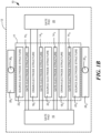
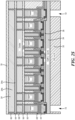
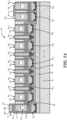
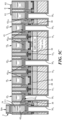
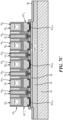
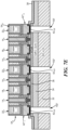
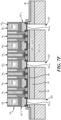
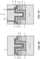
- a semiconductor structure 10 is shown having formed therein a multi-gate Field Effect Transistor (FET) 12, here a HEMT.
- the FET 12 includes a plurality of, here. for example four, gold-free, finger-like gate electrode contacts structures 14 1 -14 4 interconnected to a gold-free, gate pad 16; a plurality of, here for example, two, gold-free, finger-like drain electrode structures 18 1 -18 2 interconnected to a gold-free, drain pad 20; and a plurality of, here for example three, gold-free, source electrode structures 22 1 -22 3 interconnected by a gold-free, conductive interconnect structure 24, as shown in FIG. 1A .
- each one of the gate electrode structures 14 1 -14 4 is disposed between a corresponding one of the drain electrode structure 18 1 -18 2 and a corresponding one of the source electrode structures 22 1 -22 3 to control a flow of carriers in the semiconductor structure 10 between the corresponding one of the source electrode structures 22 1 -22 3 and the corresponding one of the drain electrode structures 18 1 -18 2 .
- two pads 26 1 , 26 2 are provided and are connected to the ends of the conductive interconnect structure 24, as shown.
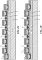
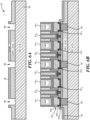
- the semiconductor structure 10 is shown in more detail to include: a substrate 32 here for example, silicon (Si), silicon carbide (SiC), or silicon on insulator (SOI).
- a layer of a Group III-N semiconductor layer 34 on an upper portion of the substrate 32 here for example, having a thickness of approximately ⁇ 1-5 microns over the upper surface of the substrate 32 followed by a second Group III-N semiconductor layer 36, here aluminum gallium nitride (Al x Ga 1-x N, where x is 0 ⁇ x ⁇ 1) for example having a thickness of approximately 5-30 nm, on the upper surface of the Group III-N layer 34.
- the layer 34 is here a GaN buffer structure, which also includes nucleation and strain relief layers, not shown; typically aluminum nitride (AlN) and aluminum gallium nitride (Al x Ga 1-x N, where x is 0 ⁇ x ⁇ 1).
- AlN aluminum nitride
- Al x Ga 1-x N aluminum gallium nitride
- Conventional silicon (Si) foundry compatible, subtractive patterning (lithography and etching) techniques is used to remove potions of the Group III-N semiconductor layer 34 and Group III-N semiconductor layer 36 to form the mesa structure shown in FIG. 1A .
- the electrical isolation provided by the etched mesa structure in FIG. 1A could also be provided by ion implantation (instead of etching), here for example nitrogen, of the same masked layer.
- the structure 10 will be processed to form a multi-gate FET 12 shown above in FIGS. 1A and 1B . It is noted that while the finger-like gate electrode structures 14 1 -14 4 , the drain electrode structures 18 1 -18 2 , and the source electrode structures 22 1 -22 3 are on the mesa 11, the gate pad 16, drain pad 20, and two pads 26 1 , 26 2 are off of the mesa 11.
- FIG. 2B the front or top side of the structure shown in FIG. 2A is coated with a passivation layer 38, here for example, silicon nitride SiN x .
- Layer 38 is processed using conventional silicon (Si) foundry compatible subtractive patterning (lithography and etching) techniques to form windows or openings 40 1 -40 7 through selected portions of layer 38 with windows 40 1 and 40 7 thereby exposing underlying surface portions of the GaN layer 34 wherein the pads 26 1 , 26 2 , gate pad 16 and drain pad 20 ( FIGS. 1A and 1B ) are to be formed and windows 40 2 -40 6 exposing underlying portions of the AlGaN layer 36 where the source electrode structures 22 1 -22 3 and drain electrode structures 18 1 -18 2 ( FIGS. 1A and 1B ) are to be formed, as shown in FIG. 2C .
- Si silicon foundry compatible subtractive patterning
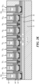
- electrical contact structures 42 1 through 42 7 are identical in construction, an exemplary one thereof, here electrical contact structures 42 1 , is shown in more detail in FIG. 3B to include: (A) a gold-free Ohmic contact structure 42 OC having: a bottom layer 42a of titanium (Ti) or tantalum (Ta); a layer 42b for example, aluminum or Si doped aluminum (Ah 1-x Si x ), where the Si doping, x, is typically ⁇ 0.05) on the layer 42a; and a layer 42c, for example tantalum (Ta) or a metal nitride, here for example titanium nitride (TiN); (B) a gold-free, electrically conductive etch stop layer 42 ES , here for example, nickel or molybdenum or platinum, disposed on the Ohmic contact structure 42 OC ; and, (C) a gold-free electrode contact, here a copper Damascene electrode contact, to be described in connection with FIG.
- an etch stop layer etches at a rate at less than one half ( ⁇ 1/2) the rate to a particular etchant than the rate such etchant etches through material being etched prior to reaching the etch stop layer.
- the layers 42a, 42b, 42c and 42 ES are disposed over the surface of the structure shown in FIG. 2C and through the openings 40 1 -40 7 ; it being noted that electrical contact structures 42 1 and 42 7 are disposed over, and are electrically connected to the two pads 26 1 , 26 2 ( FIG.
- electrical contact structures 42 2 , 42 4 , and 42 6 are disposed over, and are electrically connected to source electrode structures 22 1 -22 3 ; electrical contact structures 42 3 and 42 5 are disposed over, and electronically connected to drain electrode structures 18 1 and 18z, electrical contact structures 42 1 and 42 7 are being formed in contact with the GaN layer 34.
- the layers 42a, 42b, and 42c of the Ohmic contact structures 42 OC are formed using conventional silicon (Si) foundry compatible subtractive patterning (lithography and etching) techniques (specifically the Ohmic contact structures 42 OC are dry etched using a chlorine-based dry etch chemistry).
- the electrical contact structures 42 2 through 42 6 are then formed in Ohmic contact with the Group III-N semiconductor layer 36, here the AlGaN layer during an anneal process to be described.
- the electrical contact structures 42 1 through 42 7 is greater than 60 nm thick.
- each one of the Ohmic contact structures 42oc is a tri-metal stack and includes: (a) the bottom layer 42a of Ti or Ta (which may be recessed into the upper surface portions of the Group III-N semiconductor layer 36 for structures 42 2 -42 6 (as shown in FIG.
- the aluminum-based layer 42b here for example, aluminum or Si doped aluminum Al 1-x Si x layer 42b (where x is less than 1; here, x is typically ⁇ 0.05); and (c) the top metal layer 42c, for example tantalum or a metal nitride layer 42c, here for example titanium nitride (TiN) on the aluminum-based layer 42b layer.
- a typical thickness for layer 42a and layer 42c is 5-30 nm, while the layer 42b can range from 50-350 nm depending on the metal layers chosen for the Ohmic contact three-layer structure 42 OC stack.
- the anneal of the Ohmic contact structure 42oc to form a semiconductor Ohmic contact is kept below the melting point of aluminum ( ⁇ 660°C).
- Such low temperature anneals typically take longer than five ( ⁇ 5) minutes in a nitrogen ambient at a steady state temperature.
- a first metal element of the metal to semiconductor Ohmic contact structure 42oc here for example Ti or Ta layer 42a, is deposited directly on or disposed in contact with the Group III-N surface here for example Al x Ga 1-x N layer 36 and forms a metal nitride by reacting with the Group V element nitrogen in the Group III-N material interface layer 36 during the temperature ramp from ambient temperature to a steady state anneal temperature during the Ohmic contact formation anneal (also herein referred to as Ohmic anneal) of the Ohmic contact structure 42 OC .
- the temperature ramp is typically ⁇ 15°C/sec when a linear temperature ramp is used, however stepped temperature ramp profiles, and mixed step and linear ramp profiles all may be used in order to optimize first metal layer 42a interaction with the Group III-N surface layer 36 in the formation of the metal nitride.
- a second lower resistance metal here for example aluminum layer 42b, diffuses into the first metal (here layer 42a), the formed metal nitride, and into the surface of the Group III-N material (here layer 36) during the steady state anneal process of ⁇ 660°C for ⁇ 5 minutes to provide the lowest resistance Ohmic contact.
- any third metal layer (a metal nitride or metal, here layer 42c) disposed above the two layers (here layers 42a and 42b) and in contact with the upper layer of the two (here layer 42b).
- the prevention of intermixing of the first two layers of the Ohmic contact structure 42 OC (here layers 42a and 42b) with the third (here layer 42c) can be accomplished in several ways: First, it may be accomplished by depositing the Ohmic contact structure 42 OC and annealing the Ohmic contact structure 42 OC as a two-layer stack of the first and second metals (layers 42a and 42b) with a subsequent removal of any oxidized interface (by dry etching, wet etching, or in-situ dry sputter removal of the oxidized interface) prior to third metal deposition (here layer 42c); Second, when all three metals layers 42a, 42b and 42c of the Ohmic contact structure 42 OC are deposited prior to Ohmic anneal of the Ohmic contact structure 42 OC , one of the following two methods may be used to form a low temperature ( ⁇ 660°C) Ohmic contact between the Ohmic contact structure 42oc and the Group III-N semiconductor layer 36: In the first method, and referring to
- a metal nitride layer (such as TiN, or TaN, here layer 42c) of the Ohmic contact structure 42 OC is disposed in contact with the second aluminum layer (42b) and resists intermixing with layer 42b during the anneal at ⁇ 660°C, and metal layer 42a is alloyed with Group III-N layer 36 and metal layer 42b with a metal nitride InterLayer a, ILa, being formed between layer 42a and Group III-N layer 36, as shown in FIG.
- a thin (-1-10 nm thick) partially oxidized second metal here Aluminum layer 42b
- third metal here Ta, TiN, or TaN layer 42c
- an InterLayer b, ILb is formed by reaction with oxygen that is either present in the gases used in, or intentionally introduced into, the deposition and/or anneal apparatus during the Ohmic contact structure 42 OC deposition process or Ohmic anneal of the Ohmic contact structure 42 OC .
- This partially oxidized metal interlayer ILb is formed between the second metal layer (here aluminum layer 42b) and the third metal or metal nitride layer (here Ta, TiN, or TaN layer 42c) or in contact with the second aluminum layer (42b) which resists intermixing during the anneal at ⁇ 660°C forming post anneal Ohmic contact structure 42 OC ', as shown in FIG. 4B' .
- the second metal layer here aluminum layer 42b
- the third metal or metal nitride layer here Ta, TiN, or TaN layer 42c
- the third metal layer 42c (a metal nitride or metal) is prevented from intermixing with layer 42b during annealing by the formation of an oxide interlayer ILb during the metal deposition and/or the anneal process, and the oxide interlayer layer ILb is formed between layer 42b and layer 42c, and metal layer 42a is alloyed with Group III-N Layer 36 and metal layer 42b, and metal nitride interlayer ILa is formed between layer 42a and Group III-N layer 36 (it is noted that there may be some un-alloyed portions Un-L of layer 42a after the anneal).
- the intermixing is prevented by forming a partially oxidized interlayer ILb between the second and third metals of the Ohmic contact structure 42 OC during the electrical contact structure metal deposition and/or Ohmic anneal process.
- the intermixing is prevented by forming a metal or metal nitride layer as layer 42c.
- Silicon may be deposited by multiple methods such as electron beam deposition and sputtering. Silicon can be deposited as a separate layer within the Ohmic contact structure 42 OC (by sputtering of a Silicon sputtering target or by electron beam deposition) or by mixing Silicon into another layer by co-sputtering pure targets (here for example silicon and aluminum) or by sputtering a Si doped target (here for example Si doped aluminum Al 1-x Si x layer 42b where the Si doping, x, is typically ⁇ 0.05).
- the Ohmic contact formation anneal at the low temperature may be summarized as follows: forming a metal nitride with a first metal of the Ohmic contact structure 42 OC , here layer 42a, during a temperature ramping phase of an anneal process from ambient temperature to a steady state temperature; wherein a second metal of the electrical contact structure here layer 42b diffuses into the first metal and to an upper surface of the Group III-N semiconductor layer here layer 36 to reduce resistance of the Ohmic contact formed at the interface of Group III-N layer 36 and Ohmic contact structure 42 OC ; and wherein the first metal, in contact with the Group III-N semiconductor layer 36, and the second metal of the Ohmic contact layer 42b are prevented from intermixing with a third metal (or metal nitride) of the Ohmic contact layer 42c during the Ohmic anneal process; and wherein the first metal and the second metal and third metal (metal nitride or metal) are maintained below their melting points during the Ohmic contact formation anneal process.
- the electrically conductive etch stop layer 42 ES here for example, nickel, molybdenum or platinum is disposed on layer 42c, as shown in FIG. 3B .
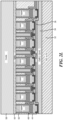
- FIG. 2E the surface of the structure shown in FIG. 2D is coated with a dielectric layer 44, here also SiN x , as shown.
- openings or windows 46 are formed in layer 44, as shown using any conventional silicon (Si) foundry compatible lithography and etch processing techniques to expose portion of the Group III-N semiconductor layer 36 where the finger-like gate electrode structures 14 1 -14 4 ( FIGS. 1A and 1B ) are to be formed, here in this embodiment, in Schottky contact with the Group III-N semiconductor layer 36, here the AlGaN layer.
- Si silicon
- the finger-like gate electrode structures 14 1 -14 4 ( FIGS. 1A and 1B ), to be described in more detail in FIG. 3A , are formed through the openings or windows 46 using silicon (Si) foundry compatible lithography and etch processes, as shown. More particularly, and each one of the gate electrode structures 14 1 -14 4 is identical in construction, an exemplary one thereof, here gate electrode structures 14 1 , is shown in detail in FIG.
- gate electrical contact structure 14 GC having a gate metal layer 14a, here a single material or plurality of materials for example nickel (Ni), titanium nitride (TiN), nickel/tantalum nitride (Ni/TaN), nickel/tantalum (Ni/Ta), nickel/tantalum/tantalum nitride (Ni/Ta/TaN), nickel/molybdenum, (Ni/Mo), titanium nitride/tungsten (TiN/W), or doped silicide in Schottky contact with the AlGaN semiconductor layer 36; and (B) gold-free electrode contact, here a copper Damascene electrode contact, to be described in connection with FIG.2K .
- A gate electrical contact structure 14 GC having a gate metal layer 14a, here a single material or plurality of materials for example nickel (Ni), titanium nitride (TiN), nickel/tantalum nitride (Ni/TaN), nickel/tantalum
- the gate metal layer 14a formed using conventional silicon (Si) foundry compatible, subtractive patterning techniques, here is a Schottky contact metal that forms the Schottky contact with the Group III-N semiconductor layer 36; it is noted that the gate electrical contact structure 14 GC may have a thin (typically -2-10 nm) dielectric layer 14b , for example aluminum oxide (Al 2 O 3 ), disposed between the gate metal layer 14a and the Group III-N semiconductor layer 36, as indicated in FIG. 3A to form an metal insulated gate HEMT (MISHEMT). It should be noted that the gate metal layer 14a may be T-shaped, as shown, or gamma-shaped ( ⁇ -shaped), as shown in FIG. 3A' , to form a field plate structure having an overhang portion 15 pointing in the direction of the adjacent drain electrode structure.
- Si silicon
- the dry etches for the metals or metal nitrides comprising Schottky gate metal layer 14a will typically be chlorine-based (to etch, for example, Ni and TiN) or fluorine-based (to etch, for example, Mo, TiN, W, Ta, and TaN) or a combination thereof (to etch for example for TiN, W, Ta, and TaN).
- etch for example, Ni and TiN
- fluorine-based to etch, for example, Mo, TiN, W, Ta, and TaN
- nickel dry etches here for example chlorine (Ch) and argon (Ar) gas mixtures, are primarily physical etches (sputtering) and not chemical-based etches.
- etching a Ni including Schottky layer 14a may result in unacceptable over etch into passivation layer 38 in some circumstances here for example when the thickness of the Ni in Schottky gate metal layer 14a and the dielectric in passivation layer 38 are about the same.
- a sacrificial dielectric layer here for example silicon dioxide (SiOz) may need to be deposited between passivation layer 38 and the overhang portion 15 of the Schottky gate metal layer 14a.
- An alternative method of etching a Schottky gate metal layer 14a comprised of Ni is to employ a dry etch for a top metal (here for example TaN, Ta, Mo or a combination thereof), if present, and a wet etch (here for example HF, H 3 PO 4 , HNO 3 , or H 2 SO 4 -based or a combination thereof) for the Ni layer. It is important to choose the Ni wet etchant of Schottky metal layer 14a such that it is highly selective to the top metal layer (if used the bottom Schottky metal layer becomes 14a' and the top Schottky layer becomes 14a" as in the description of FIGS. 10C-10G below).
- a dry etch for example TaN, Ta, Mo or a combination thereof
- a wet etch here for example HF, H 3 PO 4 , HNO 3 , or H 2 SO 4 -based or a combination thereof
- the unintended removal of the nickel underneath the masked Schottky gate metal layer 14a features should be minimized so that the gate dimensions resulting from the process are repeatable and that the gate functions as intended.
- undercut should be minimized so that the gate dimensions resulting from the process are repeatable and that the gate functions as intended.
- the thickness of the nickel layer in Schottky gate metal layer 14a will shrink as well to minimize undercut.
- the thickness of the deposited Ni of Schottky contact gate metal layer 14a is here for example likely to be ⁇ 100 nm .
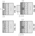
- the formation of the gate electrode structures 14 1 -14 4 is shown in more detail in connection with FIGS. 10A-10G .
- dielectric layer 44 here also SiN x
- a first gate metal or Schottky contact metal layer 14'a here for example Ni or TiN is deposited over the dielectric layer 44 and through the window 46 onto the exposed portion of the AlGaN layer 36 as shown in FIG. 10C .
- a second gate metal layer 14"a is deposited over the first gate metal or Schottky contact layer, here TaN, Ta, Mo, or W, for example, as shown in FIG. 10C .
- either a photoresist or hard mask 45 is formed over a portion of the surface of the second gate contact metal 14"a in registration with the window 46, as shown in FIG. 10D .
- the portion of the second gate contact metal 14"a exposed by the mask is removed using a dry etch, as shown in FIG. 10E .
- a dry or wet etch is used to remove the exposed portions of the first gate contact or Schottky contact metal 14'a, as shown in FIG. 10F .
- the mask 45 is then removed as shown in FIG. 10G .
- each copper Damascene electrode contacts 54 1 -54 11 occurs with the deposition of two dielectric layers (here SiN x layer 48 and SiOz layer 50) as shown in FIG. 2I .
- the first layer 48, here SiN x functions as a diffusion barrier (when copper is disposed beneath it) and an etch stop.
- the second layer, here SiOz layer 50, is etched selectively to the first layer 48, here SiN x , which is then etched to reveal gate metal layer 14a thereby forming the trenches into which a gold-free material, here copper, is subsequently deposited.
- copper Damascene electrode contacts 54 1 -54 11 are formed by first sputtering a thin metal seed layer (typically TalCu, Ta/TaN, or TaN/Cu and ⁇ 100 nm) to facilitate copper plating into trenches formed in the second dielectric layer. It is noted that the seed layer also functions as a copper diffusion barrier and as an adhesion layer to the dielectric. The excess copper overfill of the trenches is then removed with chemical mechanical polishing (CMP), which defines the metal interconnects by leaving only metal disposed in the trenches behind. As other copper Damascene layers are added, this process repeats as will be discussed below. Thus, the Damascene electrode contacts 54 1 -54 11 , have co-planar upper surfaces.
- CMP chemical mechanical polishing
- the dielectric layer 48 here for example, SiNx
- the second dielectric layer 50 here for example SiOz is deposited over layer 48 and patterned using conventional silicon (Si) foundry compatible lithography and etching techniques to form windows 52 through selected portions of layer 50 and layer 48 and thereby expose the top surfaces of the electrical contact structures 42 1 through 42 7 and the finger-like gate electrode structures 14 1 -14 4 , as shown in FIG.
- the electrode contacts 54 1 -54 11 are formed on the exposed top surfaces of the electrical contact structures 42 1 through 42 7 and the finger-like gate electrode structures 14 1 -14 4 , as shown.
- Each one of the electrode contacts 54 1 -54 11 is identical in construction; an exemplary one of the electrode contacts 54 1 -54 11 , here an electrode contact 54 2 for an exemplary one of the source or drain electrode structures 18 1 -18 2 , 22 1 -22 3 , respectively, here source electrode structure 22 1 being shown in FIG. 3B and an exemplary one of the gate electrode contacts, here gate electrode structure 14 1 being shown in FIG. 3A .
- each electrode contacts 54 1 -54 11 includes in this example an upper layer 54b of copper having the bottom and sides lined with an adhesion and copper diffusion barrier layer 54a, here for example, tantalum or tantalum nitride or a combination thereof.
- each one of the drain electrode structures 18 1 -18 2 and each one of the source electrode structures 22 1 -22 3 is a multi-layer, electrical contact structure in contact with the Group III-N semiconductor layer 26 and includes: a gold-free contact layer 42 OC in Ohmic contact with the Group III-N semiconductor layer 26; a gold-free electrically conductive etch stop layer 42 ES electrically connected to the gold-free contact layer 42 OC ; and, one of the gold-free Damascene electrode contacts 54 2 , 54 4 , 54 6 , 54 8 and 54 10 .
- each one of the gate electrode structures 14 1 -14 4 includes a gold-free gate electrical contact and one of the gold-free Damascene electrode contacts 54 3 , 54 5 , and 54 7 .
- each one of the Damascene electrode contacts 54 2 -54 10 are identical in construction and all eight Damascene electrode contacts 54 2 -54 10 are formed simultaneously.
- a dielectric layer 56 here silicon nitride (SiNx) is deposited over the surface and then layer 56 is covered with a second dielectric layer 58, here an oxide layer 58, here for example silicon dioxide.
- the layers 56 and 58 are patterned using conventional silicon foundry compatible lithography and etch processing techniques to have openings or windows 60 1 -60 5 formed there-through over the source electrode structures 22 1 -22 3 ( FIG. 1B ) and pads 26 1 and 26 2 ( FIG. 1B ) and thereby expose the tops of the electrode contacts e 54 1 , 54 2 , 54 6 , 54 10 and 54 11 , as shown.
- upper electrical interconnects 62 1 -62 5 are formed in the windows 60 1 -60 5 respectively using conventional silicon foundry compatible processing techniques thereby making electrical connection to electrode contacts 54 1 -54 11 54 1 , 54 2 , 54 6 , 54 10 and 54 11 , respectively, and hence to the source electrode structures 22 1 -22 3 ( FIG. 1B ) and pads 26 1 and 26 2 ( FIG. 1B ).
- Each one of the upper electrical interconnects 62 1 -62 5 is constructed the same as each one of the electrode contacts 54 1 , 54 2 , 54 6 , 54 10 and 54 11 and includes an upper layer 62b of copper having the bottom and sides lined with an adhesion and copper diffusion barrier layer 62a, here for example, tantalum (Ta) or tantalum nitride (TaN) or a combination thereof.
- an adhesion and copper diffusion barrier layer 62a here for example, tantalum (Ta) or tantalum nitride (TaN) or a combination thereof.
- a dielectric layer 64 here SiNx is formed over the structure shown in FIG. 2M followed by a dielectric layer 66 of silicon dioxide.
- a window 68 is formed through a selected portion of the layers 64, 66 to expose the tops of upper electrical interconnects 62 1 -62 5 .
- the conductive interconnect structure 24 ( FIGS. 1A , 1B ) is formed like the upper electrical interconnects 62 1 -62 5 includes an upper layer 24b of copper having the bottom and sides lined with an adhesion and copper diffusion barrier layer 24a, here for example, tantalum or tantalum nitride or a combination thereof.
- a dielectric layer 70 here SiN x is formed over the surface of the structure shown in FIG. 2Q .
- additional Cu-based interconnect layers may be added in a manner identical to the Cu interconnect layers described above.
- a test pad layer or Input/Output pads may be added for facilitate final testing or connection to other circuits (not shown), respectively.
- front-side processing is complete.
- the back-side processing begins. More particularly the wafer is mounted face down on a temporary carrier, not shown, the wafer is then thinned, here for example to 50 or 100 microns. The exposed bottom surface of such structure is masked to expose portions of the bottom of the substrate 32 under the electrode contacts 54 1 and 54 11 . Next, via holes 72 are formed in the exposed portions by etching from the bottom of the SiC or Si substrate 32 using a dry fluorine-based etch, here, for example sulfur hexafluoride (SF 6 ).
- SF 6 sulfur hexafluoride
- the bottom surface of substrate 32 is exposed to a dry chlorine-based etch, here for example a combination of boron tri-chloride (BCl 3 ) and chlorine (Ch), to continue the depth of via holes 72 (as indicated by the arrows 74) by etching through the exposed portions of the Group III-N layer 34 and then through exposed inner portions of the Ti or Ta layer 42a, then through inner portions of the aluminum-based layer 42b, then through exposed inner portions of the metal nitride layer 42c of the Ohmic contact structures 42 OC of the electrode contacts 54 1 and 54 11 ; the etching then stopping at the etch stop layer 42 ES on the electrical contact structures 42 under the electrode contacts 54 1 and 54 11 , as indicated.
- a dry chlorine-based etch here for example a combination of boron tri-chloride (BCl 3 ) and chlorine (Ch)
- the bottom of the structure of FIG. 2T has the conductive layer 28 ( FIG. 1A ) disposed on the bottom of substrate 32 and into via hole, 72.
- the layer 28b is copper with an adhesion and copper diffusion barrier layer 28a, here for example, tantalum or tantalum nitride or a combination thereof (as shown in FIG. 2U' ) to form the conductive vias 30 1 and 30 2 ( FIG. 1A ) and a ground plane conductor 30 3 .
- the conductive vias 30 1 and 30 2 electrically interconnect the ground plane conductor 30 3 to the front side metallization layers and ultimately to the interconnect source electrode structures 22 1 -22 3 through etch stop layer 42 ES to bottom of electrode contacts 54 1 and 54 11 ( FIGS. 1A and 1B ).
- the conductive vias 30 1 and 30 2 and ground plane 30 3 can have layer 28 comprised of alternate metals here, for example a gold (Au) layer 28b, and a titanium (Ti) or titanium/platinum (Ti/Pt) layer 28a. In this case, the back-side processing would be performed in an area where gold would not present any contamination problems.
- a back-side via hole 72 is formed using chemical dry etching with a two-step etch process that terminates on the electrically conductive etch stop layer 42 ES .
- via holes are formed in exposed portions of the bottom of the SiC or Si substrate layer 32 using a dry fluorine-based etch for example, sulfur hexafluoride (SF 6 ). This fluorine-based etch stops selectively on Group III-N layer 34 such as gallium nitride (GaN) and aluminum nitride (AlN).
- the bottom surface of the exposed Group III-N layer in the via hole 72 is exposed to a dry chlorine-based etch, for example a combination of boron tri-chloride (BCl 3 ) and chlorine (Cl 2 ).
- a dry chlorine-based etch for example a combination of boron tri-chloride (BCl 3 ) and chlorine (Cl 2 ).
- This chlorine-based back-side via hole 72 dry etch continues the via hole etching through the Group III-N layers 34 and 36 (in the example shown in FIG. 2 , "off' mesa etches only need to etch through Group III-N layer 34 after etching through substrate layer 32) and the metal to semiconductor electrical contact structure and terminates on the conductive etch stop layer 42 ES here for example nickel or molybdenum or platinum.
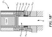
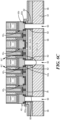
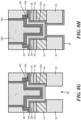
- FIG. 5A through 5C here an embodiment is described of a portion of a MMIC structure 10', here for example having, as shown in more detail in FIG. 5A , a multi-gate HEMT FET, having: electrode contacts 54 2 , 54 6 and 54 10 disposed on electrical contact structures 42 2 , 42 4 and 42 6 , respectively, as shown to provide gold-free source electrode structures 22 1 -22 3 in Ohmic contact with Group III-N semiconductor layer 36 and interconnected with gold-free conductive vias 30 1 -30 3 ( FIG.
- electrode contacts 54 4 , and 54 8 disposed over electrical contact structures 42 3 , and 42s, respectively, as shown to provide gold-free drain electrodes structures 18 1 , 18 2 in Ohmic contact with Group III-N semiconductor layer 36 and interconnected to the gold-free drain pad 20 ( FIG. 1B ) and electrode contacts 54 3 , 54 5 , 54 7 and 54 9 disposed over gold-free gate electrode structures 14 1 -14 4 , respectively in Schottky contact with the Group III-N semiconductor layer 36 and connected to gate pad 16 ( FIG. 1B ).
- the structure 10' includes: a resistor R, here for example tantalum nitride (TaN), having a pair of electrodes (the opposing ends of the resistor R) R1 and R2; one of the electrodes, R1, being connected to electrode contact 54 11 , electrical contact 42 7 and then to the conductive layer 28 by a conductive via 30 4 ( FIG.
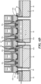
- the thickness of the copper forming the lower plate C1 of the capacitor C and used for the resistor R is thicker than that used for the source electrode structures 22 1 , 22 2 and 22 3 and drain electrode structures 18 1 and 18 2 for two reasons: First, the trenches formed during Damascene processing have to be deeper (unless ion implantation isolation instead a mesa as noted above, which is not shown, is used to enable planar structures) to enable "off' mesa 11 ( FIGS. 1B and 2A ) vertical interconnects to "on" mesa 11 electrical contact structures 42. Second, all contacts formed during metal layer deposition terminate at the same level on the upper surface of the layer due to the CMP process.
- the electrical contact structures 42 1 -42 8 are formed in the same manner described above in connection with FIGS. 2A-2T .
- the source electrode structures 22 1, 22 2 and 22 3 and drain electrode structures 18 1 and 18 2 are in Ohmic contact with the Group III-N semiconductor layer 36 and the gate electrode structures 14 1 , 14 2 and 14 3 are in Schottky contact with the Group III-N semiconductor layer 36.
- the back-side processing proceeds as in FIGS. 2S and 2T . More particularly, the wafer is mounted face down on a temporary carrier, not shown, the wafer is thinned, here for example to 50 or 100 microns.
- the exposed bottom surface of such structure is masked with mask 78 and processed using conventional silicon compatible processing techniques to expose portions of the bottom of the substrate 32 disposed under the central or inner surface portions of the electrical contact structures 42 1 , 42 2 , 42 4 , 42 6 and 42 7 , as shown, followed by, first a dry fluorine-based etch, here, for example SF 6 , as described above in connection with FIG 2S to etch via holes 72 through exposed portions of the substrate 32 and then a dry chlorine-based etch, here for example a combination of boron tri-chloride (BCl 3 ) and chlorine (Clz), to continue the depth of via holes 72 by etching through the exposed portions of Group III-N layers 34 and 36, then through the central or inner portions 79 IP , as shown for
- the mask 78 is removed and the back-side process is performed as described in connection with FIG. 2U .
- the bottom of the structure of FIG. 5B has conductive layer 28 formed over it and over the sides and bottom surface of then extended via holes 72, as described above in connection with FIG. 2U' to form conductive vias 30 1 -30 5 over the exposed electrically conductive etch stop layers 42 ES to electrically interconnect the source electrode structures 22 1 -22 3 , the bottom plate C1 of capacitor C and the electrode R1 of resistor, as shown.
- the electrical contact structures 42' could be a single Ohmic contact layer 42' OC , here a silicide layer, here for example nickel silicide (NiSi) or cobalt silicide (CoSi 2 ), as shown in FIG. 5A' .
- the silicide layer Ohmic contact structure 42' OC may also be doped to further improve contact resistance.
- NiSi for example it could be doped with phosphorus (P), arsenic (As), antimony (Sb) or a combination thereof.
- Si and Ni or Co is deposited, etched back and then alloyed.
- the alloy temp here for example is ⁇ 450°C.
- Ohmic contact structure 42' OC may be recessed into the Group III-N semiconductor layer 36 so that the bottom surface of silicide layer Ohmic contact structure 42' OC is 2-20 nm from the bottom surface of the Group III-N layer 36. It is noted that the etch stop layer 42 ES is disposed on the Ohmic contact structure 42' OC , as shown.
- the electrical contact structure includes an Ohmic contact structure 42' OC having an etch stop layer 42 ES on the Ohmic contact structure 42' OC .
- a structure 10" is shown having substrate 32 here for example, Si or SiC; a mesa shaped (defined by etching or implant isolation, as noted above), Group III-N semiconductor layer 34 on an upper portion of the substrate 32, here Group III-N layer 32 is, for example, a layer of gallium nitride (GaN) having a thickness of approximately 1-5 microns over the upper surface of the substrate 32, as shown, and a Group III-N semiconductor layer 36, here Al x Ga 1-x N, for example having a thickness of approximately 5-30 nm, on the upper surface of Group III-N layer 34.
- GaN gallium nitride
- apertures 80 are etched, using conventional silicon foundry compatible subtractive patterning (lithography and etching) techniques and here, for example a combination of boron tri-chloride (BCl 3 ) and chlorine (Cl 2 ) dry etching, in portions of the Group III-N layers 34 and 36 where electrically conductive vias 90, to be described in connection with FIGS. 6B and 6C , are to be formed to electrically interconnect the sources electrode structures 22 1 -22 3 ( FIG. 1B ).
- BCl 3 boron tri-chloride
- Cl 2 chlorine
- the apertures 80 are filled with a semiconductor or dielectric or metal material 82 that can be dry etched in fluorine containing gasses, here for example SiNx, SiO 2 , molybdenum or polysilicon or a combination thereof.
- a semiconductor or dielectric or metal material 82 that can be dry etched in fluorine containing gasses, here for example SiNx, SiO 2 , molybdenum or polysilicon or a combination thereof.
- the structure is processed as described above in connection with FIGS. 2B-2K to form electrical contact structures 42" 1 -42" 5 ; it being noted that here the electrical contact structures 42" 1 -42" 5 do not include a separate etch stop layer, such a etch stop layer 42 ES as described above in connection with FIGS.
- Electrode contacts 54 1 , 54 3 , 54 5 , 54 7 and 54 9 respectively are disposed on the top of Ohmic contact structures 42 OC1 -42 OC5 , respectively, as indicated.
- Electrical contact structures 42" 1 , 42" 3 and 42" 5 are for the source electrode structures 22 1 -22 3 and electrical contact structures 42" 2 and 42'4 are drain electrode structures 18 1 , 18 2 ( FIG.
- the bottom surface of the electrical contact structures 42" 1 , 42" 3 and 42" 5 are larger in surface area than the surface area of the semiconductor or dielectric or metal material 82, with the outer surface portions of the electrical contact structures 42" 1 , 42" 3 and 42" 5 being in Ohmic contact with the Group III-N semiconductor layer 36, as shown.
- Gate electrode structures 14 1 -14 4 are in Schottky contact with the Group III-N semiconductor layer 36, as shown, and have thereon electrode contacts 54 2 , 54 4 , 54 6 , and 54 8 , as shown.
- Ohmic contact structure layers 42a, 42b, and 42c of the electrical contact structures 42" 1 -42" 5 and the electrode contacts have been described above in connection with FIG. 3B with the Ohmic contact structure 42 OC1 -42 OC5 having: a bottom layer 42a of Ti or Ta (which may be recessed into the upper surface portions of the Group III-N semiconductor layer 36); a middle layer 42b of an aluminum-based layer, here aluminum or Si doped aluminum Al 1-x Si x layer ; and an upper layer 42c of tantalum or metal nitride layer, here for example tantalum (Ta), tantalum nitride (TaN) or titanium nitride (TiN) on the aluminum or Si doped aluminum Al 1-x Si x layer; and the electrode contacts 54 1 -54 9 having an electrically conductive metal interconnect contact, here for example copper having the sides and bottom lined with a diffusion barrier layer, here for example, tantalum or tantalum nitride or a combination thereof.
- etch stop layer 42 ES there is no separate etch stop layer 42 ES (described above in connection with FIGS. 2A-2U ); rather, because of the fluorine chemical etchant used to form the vias 90 ( FIG. 6C ) in this embodiment, the etch stop layer is provided by layer 42b, here for example aluminum (or Si doped Aluminum Al 1-x Si x , of electrical contact structures 42".
- the back-side processing proceeds as in FIG. 2U . More particularly the wafer is mounted face down on a temporary carrier, not shown, the wafer is thinned, here for example to 50 or 100 microns.
- the exposed bottom surface of such structure is masked by a mask 96 ( FIG. 6C ) to expose portions of the bottom of the substrate 32 under the source electrode structures 22 1 -22 3 .
- a mask 96 FIG. 6C
- outer peripheral portions of the semiconductor or dielectric or metal material 82 are covered by the mask 96; and hence under the inner portions 81 IP ( FIG. 6C' ) of the electrical contact structures 42 while the other portions 81 OP of the electrical contact structures 42 remain in Ohmic contact with layer 36.
- vias 90 are etched using a dry fluorine-based etch, here for example SF 6 to etch the vias 90 through the substrate layer 32 and through the inner portions of the material 82 (here for example SiNx, SiO2, molybdenum or poly silicon in FIG. 6C' ), inner portions 81 IP of the bottom layer 42a of Ti or Ta (which may be recessed into the upper surface portions of the Group III-N semiconductor layer 36) and then stopping at inner portions of the Aluminum-based layer 42b whose fluorine-based etch byproducts are nonvolatile.
- a dry fluorine-based etch here for example SF 6 to etch the vias 90 through the substrate layer 32 and through the inner portions of the material 82 (here for example SiNx, SiO2, molybdenum or poly silicon in FIG. 6C' ), inner portions 81 IP of the bottom layer 42a of Ti or Ta (which may be recessed into the upper surface portions of the Group III-N semiconductor layer 36) and then stopping at inner portions of the
- the bottom of the structure of FIG. 6C has a conductive layer 28, here for example copper-based, is formed over it and over the sides and bottom surface of then extended via holes 90 to form conductive vias 96 and a ground plane conductor 95, as described above in connection with FIG. 2U , for the structure to electrically interconnect the inner or central portions of the electrical contact structures 42" as shown, and therefore interconnect the source electrode structures 22 1 -22 3 .
- the Group III-N material is etched from the front-side of the wafer, as described above in connection with FIG. 6A prior to back-side processing and via 90 formation.
- the apertures 80 FIG.
- a material layer 82 (here for example SiNx, SiO 2 , molybdenum or polysilicon) that can be etched with fluorine-based dry etch chemistries.
- a material layer 82 here for example SiNx, SiO 2 , molybdenum or polysilicon
- fluorine-based dry etch chemistries Assuming that all the layers that need to be etched to form the via 90 are now the substrate 32 (silicon, silicon carbide (SiC), silicon dioxide (SiOz), silicon nitride (SiN x ) or a combination thereof) and the aperture semiconductor or dielectric or metal material 82 (here for example SiNx, SiO2, molybdenum or polysilicon), those layers can now all be etched using the fluorine-based etchants. As a result, a fluorine-based etch is then used for the entire via etch process.
- FIG. 6D' another embodiment is described.
- the via 96 is etched wider than in FIG. 6D ; however, here again the etching stops at the inner portions of the Aluminum based layer 42b.
- layer 42b functions as an etch stop layer.
- Fig. 6D' there is no remaining dielectric layer 82 in the via 90 (as shown in Fig. 6C' ).
- FIGS. 7A-7G another embodiment is shown.
- the structure 10'" shown in FIG. 2B is processed as described in connection with FIG. 2C except only windows 40 2 -40 6 are formed, as shown.
- an etch stop layers 42 ES ' here for example, silicon dioxide or SiN x , are formed using conventional silicon (Si) foundry compatible (subtractive) lithography and etch processing techniques, on the inner surface portions of layer 36 exposed by the windows 40 2 , 40 4 , 40 6 ; it being noted in FIG. 7B that outer surface portions of the exposed surface of layer 36 are void of the etch stop layers 42 ES '.
- etch stop layers 42 ES ' could be formed on the inner surface portions of layer 36 exposed by all windows 40.
- layers 42a, 42b and 42c are now formed over the etch stop layers 42 ES '; it being noted that outer peripheral portions of the layers 42a, 42b and 42c are in direct contact with layer 36.
- Ohmic contact is formed between the outer peripheral portions of layers 42a, 42b and 42c and Group III-N layer 36.
- the electrical contact structures 42′′′ 1, 42′′′ 3 ,and 42′′′ 5 include an etch stop layer, here etch stop layer 42 ES ', that is under the inner portions of layers 42a, 42b and 42c; rather than on top of layers 42a, 42b, and 42c.
- etch stop layer 42 ES ' included etch stop layer 42 ES on top of layer 42c (on top of the electrical contact structure 42); here, as shown in FIG. 3B' , the etch stop layer 42 ES ' of the electrical contact structure 42' used in FIGS. 7A-7F is under the inner or central portion of layer 42a of the electrical contact structure 42′′′).
- electrode contacts 54 1 -54 9 simultaneously form the upper layers of the source electrode structures 22 1 -22 3 , drain electrode structures 18 1 , 18 2 , and gate electrode structures 14 1 -14 4 , as shown.
- the back-side processing begins. More particularly the wafer is mounted face down on a temporary carrier, not shown, the wafer is then thinned, here for example to 50 or 100 microns. The bottom surface of the structure is masked with windows therein disposed under the etch stop layers 42 ES '. An etchant, here for example, fluorine, is used to etch via 102 through the substrate 32, as shown.
- a temporary carrier not shown
- a chlorine-based etchant such as BCl 3 and Clz are used to extend the vias 102 to via 102'; as shown, such etching stopping at the etch stop layers 42 ES ', as shown.
- the etch stop layer 42 ES ' is removed from the bottom of the via hole 102' using dry etch chemistries that are fluorine-based when either SiOz or SiN x is used as a layer 42 ES ' etch stop. Fluorine-based wet etches are suitable for removing SiOz and Al 2 O 3 layer 42 ES ' etch stops, and some SiN x layer 42 ES ' etch stops, as shown in FIG. 7F .
- a conductive layer 28 is formed over the bottom of the structure as described above in connection with FIG. 2U to electrically interconnect the source electrode structures 22 1 -22 3 .
- FIGS. 8A-8F another embodiment is shown for forming an Ohmic contact to one of the source electrode structures and the connection of the source electrode structure to back-side metallization conductive layer 28.
- a window 200 is formed through the dielectric layer 38, underlying portions of AlGaN layer 36, and GaN layer 34 to the surface of the substrate 32, as shown in FIG. 8B , here using conventional lithography and dry etch processes, here for example the chlorine-based etchants BCl 3 and Cl 2 .
- the electrical contact structure 42' having layers 42a, 42b and 42c of the Ohmic contact structure 42 OC are sequentially deposited and patterned as shown using conventional lithographic-etching process as described above in connection with FIG. 2D , the Ohmic contact structure 42 OC having: a bottom layer 42a of titanium (Ti) or tantalum (Ta); a layer 42b for example, aluminum or Si doped aluminum Al 1-x Si x (where the Si doping, x, is typically ⁇ 0.05) on the layer 42a; and a layer 42c, for example tantalum (Ta) or a metal nitride, here for example titanium nitride (TiN).
- Ohmic contact regions 110 FIG. 8C between the Ohmic contact structure 42 OC and sidewalls of the AlGaN layer 36.
- the dielectric layers 44 and 48 are formed as shown in FIG. 8D , as described above in connection with FIGS. 2F through 2H .
- the Damascene process begins by depositing the dielectric layer 50 as described above in connection with FIGS. 2I , as shown in FIG. 8E , followed by the formation of the electrical interconnect including, in this example the upper layer 54b of copper having the bottom and sides lined with an adhesion and copper diffusion barrier layer 54a, here for example, tantalum or tantalum nitride or a combination thereof as described above in connection with FIGS. 2I-2L , resulting in an exemplary one of the above described Damascene electrode contacts 54 1 -54 11 , here indicated without a subscript as 54, as shown in FIG. 8F .
- the electrical interconnect including, in this example the upper layer 54b of copper having the bottom and sides lined with an adhesion and copper diffusion barrier layer 54a, here for example, tantalum or tantalum nitride or a combination thereof as described above in connection with FIGS. 2I-2L , resulting in an exemplary one of the above described Damascene electrode contacts 54 1 -54 11 , here indicated
- the wafer is mounted face down on a temporary carrier, not shown, the wafer is thinned, here for example to 50 or 100 microns.
- the exposed bottom surface of such structure is masked to expose portions of the bottom of the substrate 32 under the source electrode structure.
- vias 90 are etched using a dry fluorine-based etch, here for example SF6 to etch the vias 90 through the substrate layer 32 and through the bottom layer 42a of Ti or Ta and then stopping at the aluminum-based layer 42b whose fluorine-based etch byproducts are non-volatile.
- a dry fluorine-based etch here for example SF6 to etch the vias 90 through the substrate layer 32 and through the bottom layer 42a of Ti or Ta and then stopping at the aluminum-based layer 42b whose fluorine-based etch byproducts are non-volatile.
- etch stop layer 42 ES there is no additional (separate) etch stop layer 42 ES ; rather layer 42b functions as an etch stop layer
- the bottom of the structure of FIG. 8G has a conductive layer 28 in electrical connection with the layer 42b of the electrical contact structure 42', as described above in connection with FIGS. 2S-2U .
- FIGS. 9A-9E another embodiment is shown.
- the window 200 is formed through the dielectric layer 38, underlying portions of AlGaN layer 36, and GaN layer 34 to the surface of the substrate 32, as shown in FIG. 9B , here using conventional lithography and dry etch processes, here for example the chlorine-based etchants BCl 3 and Cl 2 .
- the window 202 is etched with a fluorine-based dry etchant that laterally etches dielectric layer 38 (as shown in FIG. 9C ) to expose a surface portion of Group III-N semiconductor layer 36 around the edge of the window 200 (as shown in FIG. 9B ).
- layers 42a, 42b, 44 and 48 are formed as described in connection with FIGS. 8C and 8D after which the process continues as described above in connection with FIGS. 8E and 8F .
- the metal to semiconductor Ohmic contact structure 42oc' may comprise a two or more layer stack of Al with Ta, Ti, TiN, Pt, Ni, Si, AlSi, W, or Mo such as Ta/Al, Ti/Al, Ta/Al/Ta, Ta/ Al 1-x Si x /Ta, Ta/Al/TiN Ta/Al/Ni, Ti/Al/Ni, Ta/Al, Ti/Al, Ti/Al/W, Ti/Al/Mo, Ti/Al/Pt.
Landscapes
- Junction Field-Effect Transistors (AREA)
- Electrodes Of Semiconductors (AREA)
- Chemical & Material Sciences (AREA)
- Engineering & Computer Science (AREA)
- Materials Engineering (AREA)
- Physics & Mathematics (AREA)
- Geometry (AREA)
Description
- This disclosure relates generally to a structure having a gold-free electrical contact structure in contact with an upper surface of a Nitride.
- As is known in the art, many monolithic microwave integrated circuits (MMICs) having Group III-Nitride semiconductors, sometimes referred to as nitride semiconductors, such as for example, gallium nitride-based (AlGaN/GaN) high electron mobility transistors (HEMTs), are increasingly being used for high-frequency and highpower applications. Group III-Nitride are herein after sometimes also referred to as Group III-N which includes, for example, binaries InN, GaN, AlN, their ternary alloys such as AlxGa1-xN (AlGaN) alloys and other nitrogen based alloys.
- In order to realize the potential of these HEMT devices it is necessary to achieve low-resistance, good edge acuity and reliable metal to metal contacts, and metal to semiconductor Ohmic contacts. Most Group III-N foundry metal to metal and metal to semiconductor low resistance Ohmic contacts use gold (Au) to reduce sheet resistance (for transmission lines and Ohmic contacts) and to decrease oxidation during the high temperature anneal required to achieve the lowest metal to semiconductor Ohmic contact resistance to active devices.
- As is also known, in many Monolithic Microwave Integrated Circuits (MMICs) and other integrated circuits (ICs), electrical connection is made to the bottom of the MMIC for both ground and electrical signals to mounted chips, these connections are made through electrically conductive vias passing through the substrate and/or a semiconductor epitaxial layer on at least a portion of the substrate to electrical contacts that connect the vias to a metallization on the wafer; sometimes referred to as a front-side metallization.
- Traditionally, Group III-N HEMT MMICs and devices are fabricated by liftoff-based processing in III-V foundries. Recently, however, Group III-N HEMTs have begun to be fabricated using high yield silicon (Si) like, Au-free, subtractive processing techniques in Si CMOS foundry environments. More particularly, a "lift-off" process is where a mask has a window to expose a selected portion of a surface where a material is to be deposited. The material is deposited onto the mask with a portion of the material passing through the window onto the exposed selected portion of the surface. The mask is lifted off the surface with a solvent along with portion of the material on the mask (the unwanted portion of the deposited material) while leaving the desired portion of the material on the exposed selected portion of the surface. A "subtractive" process is where a material is first deposited over the entire surface. Then a mask is formed to cover only over a selected portion of the deposited material (the portion which is to remain after the processing); the unwanted portions of the deposited material being exposed. An etchant is then brought into contact with the mask thereby removing the exposed unwanted portion while the mask prevents the etchant from removing the covered desired portion of the material.
- Relative to Si CMOS foundries, it is well known that the yield and cost of III-V compound semiconductor devices and circuits (processed in traditional III-V foundries) has long been limited by low wafer volumes, increased substrate handling during processing, the widespread use of liftoff-based processing techniques to define metal lines, and the use of time consuming electron beam lithography for sub 500 nm gate lithography. The Si CMOS foundry environment on the other hand has the benefit of high wafer volumes, large wafer diameters (≥200 mm), highly automated cassette to cassette wafer fabrication or processing tools, subtractive processing techniques, advanced optical lithography cluster tools and techniques (capable of defining sub 100 nm features), and the Moore's law paradigm that drives both equipment development and technology node development.
- However, as noted previously, to take advantage of the benefits of the Si foundry infrastructure and background Si CMOS wafer volumes, the developed Group III-N processes have to be Au-free. Gold is a deep level trap dopant in Si. Therefore, Au is not allowed in the front end or back end of Si CMOS foundry fabrication lines as it is a serious contamination concern that can cause catastrophic yield problems.
- Gold free processing of GaN (or other III-V) device wafers in Si foundry environments therefore requires the use of Si foundry back end of line (BEOL) compatible metallizations such as aluminum (Al) or copper (Cu). Copper is the most attractive of these metals to use as it has superior electrical conductivity and electro-migration resistance. However, because of the lack of volatile copper dry etch byproducts, copper cannot readily be subtractively patterned by the techniques of photolithography wherein photoresist masking and plasma etching have been used with great success with aluminum. To process copper, the Damascene process (which is also subtractive), was developed. In the Cu Damascene process, a host insulator material for the copper, typically an underlying insulating layer (usually silicon dioxide), is patterned with open trenches where the copper is to be formed. A thick coating of copper that significantly overfills the trenches is deposited on the insulating layer, and chemical-mechanical planarization (CMP) is used to remove the excess copper that extends above the top of the insulating layer. Cu filled within the trenches of the insulating layer is not removed and becomes the patterned conductive interconnect.
- As is also known in the art, while Cu is manageable, it also poses its own contamination risk for Si foundries. Barrier layers should completely surround all copper interconnections, since diffusion of copper into surrounding materials would degrade their properties. Typically, the trenches are lined with thin tantalum (Ta) and /or tantalum nitride (TaN) metal layers (as part of the Ta/TaN/Cu plating seed metal stack) to act as diffusion barriers along the bottom and sides of the Cu metal interconnects. At post Cu CMP the top of the interconnect metal is coated with SiNx to act as the top interface diffusion barrier, to prevent oxidation during interlayer oxide deposition, and to act as a stop etch layer (during the trench etch of the silicon dioxide) for additional interconnect formation. Additional process complications arise, however, when back to front side metal interconnects are facilitated by through-wafer or through-semiconductor layer vias that require a chlorine-(or other oxidizer) based etches to form these vias. The chloride-based etch by-products are nonvolatile and the etch process results in a degraded Cu interfacial surface.
-
EP2996155A1 describes a semiconductor device including a semiconductor substrate, a semiconductor element, and wiring. The semiconductor element has an electrode provided on a surface of the semiconductor substrate. The electrode includes a junction layer joined to the surface of the semiconductor substrate, a diffusion-suppressing layer provided on the junction layer, and a pad layer provided on the diffusion-suppressing layer. The wiring is provided on a back surface of the semiconductor substrate and on an inner surface of a through hole which penetrates the semiconductor substrate immediately below the electrode. The wiring is electrically connected to the electrode. - In accordance with the disclosure, a semiconductor structure is provided as defined in appended
claim 1. - In one embodiment, the multi-layer, electrical contact structure comprises an aluminum-based layer disposed over the gold-free contact layer.
- In one embodiment, the gold-free contact layer is in direct contact with the Group III-N semiconductor layer and wherein the gold-free contact layer and the aluminum-based layer have physical annealing properties enabling annealing with the Group III-N semiconductor layer at a temperature less than 660 degrees to form an Ohmic contact with the Group III-N semiconductor layer.
- In one embodiment, a method is provided for forming a semiconductor structure as defined in appended
claim 4. - In one embodiment, the contact layer is formed in direct contact with the Group III-N semiconductor layer and wherein the contact layer and the aluminum-based layer are annealed at a temperature less than 660 degrees to form an Ohmic contact with the Group III-N semiconductor layer
- In one embodiment, the etch stop layer comprises aluminum, nickel, molybdenum, platinum, or aluminum.
- In one embodiment, the electrical contact structure a two or more layer stack of Al with Ta, Ti, TiN, Pt, Ni, Si, AlSi, W, or Mo.
- In one embodiment, the electrical contact structure comprises a metal silicide
- In one embodiment, the electrical contact structure comprises the metal silicide is CoSi2 or NiSi.
- In one embodiment, the metal silicide is recessed within the Group III-N semiconductor layer.
- With such arrangements, silicon foundry compatible, subtractively patterned through substrate via (TSV) etch stop metal layers are placed on the front side of the wafer between the front side gold-free metal interconnect contact structure and the back-side etched via. Metals such as nickel or molybdenum or platinum are used as the etch stop layer for chlorine-based back-side via etches, while aluminum can act as an etch stop for fluorine-based etches. These metal etch stop layers are as thin as possible in order to mitigate negative impact on the front to back-side resistance of the interconnect contact structure.
- In one embodiment, the electrical contact structure includes the electrically conductive etch stop layer disposed above the third metal layer (the layer that prevents intermixing) of the electrical contact structure. In this embodiment, after front-side processing and back-side wafer thinning, back-side via holes are formed using chemical dry etching with a two-step etch process that terminates on the electrically conductive etch stop layer. In the first step of the via hole etch process, via holes are formed in the exposed portions of the bottom of the substrate using a dry fluorine-based etch. This fluorine-based etch stops selectively on Group III-N layers. In the second step, the bottom surface of the exposed Group III-N layer in the via hole is exposed to a dry chlorine-based etch. This chlorine-based back-side via hole dry etch continues the via hole etching through the Group III-N layers and the electrical contact structure and terminates on the conductive etch stop layer of the electrical contact structure metal.
- In one embodiment one of the first three metals of the electrical contact structure is also the electrically conductive etch stop layer and the chemical etching comprises forming the via hole with a single fluorine-based etchant through the substrate and a dielectric layer. In this embodiment, prior to electrical contact structure deposition, the Group III-N material is etched selectively to the substrate to form openings (apertures) in the Group III-N material wherein the via holes are to be formed. The apertures are then filled with a dielectric material that can be etched in fluorine-based chemistries just as the substrate. The electrical contact structure, one of whose first three layers includes an etch stop layer to fluorine-based chemistries, is then deposited and the remainder of front-side processing continues. As a result, during back-side processing, a single fluorine-based dry etch can be used to etch via holes selectively through the substrate and aperture dielectric to the etch stop layer embedded within electrical contact structure.
- In one embodiment one of the first three metals of the electrical contact structure is also the electrically conductive etch stop layer and the chemical etching comprises forming the via hole with a single fluorine-based etchant through the substrate layer. In this embodiment, prior to electrical contact structure deposition, the Group III-N material is etched selectively to the substrate to form openings (apertures) in the Group III-N material wherein the via holes are to be formed. The electrical contact structures are then deposited into the apertures (therefore directly contacting the substrate at the bottom of the apertures) and the remainder of front-side processing continues. As a result, during back-side processing, a single fluorine-based dry etch can be used to etch via holes selectively through the substrate to the etch stop layer embedded within electrical contact structure.
- The details of one or more embodiments of the disclosure are set forth in the accompanying drawings and the description below. Other features, objects, and advantages of the disclosure will be apparent from the description and drawings, and from the claims.
-
-
FIG. 1A is a simplified cross-sectional sketch of a Field Effect Transistor (FET), here a high electron mobility transistor (HEMT), according to the disclosure; -
FIG. 1B is a simplified plan view of a portion of the FET ofFIG. 1A , such plan view being taken alongline 1B-1B ofFIG. 1A ; -
FIGS. 2A-2U are diagrammatical, cross-sectional sketches at various stages in the fabrication of a semiconductor structure at various stages in the fabrication thereof according to the disclosure, whereFIG. 2U' is an exploded diagrammatical cross-sectional view of a portion ofFIG. 2U indicated by thearrow 2U'-2U'; -
FIG. 2D' is an enlarged portion ofFIG. 2D , such enlarged portion being encircled by an arrow inFIG. 2D ; -
FIG. 3A is a diagrammatical, cross-sectional sketch of an exemplary one of a plurality of gate electrode structures used in the structure ofFIGS. 2A through 2T according to the disclosure; -
FIG. 3A' is a diagrammatical, cross-sectional sketch of another embodiment of an exemplary one of a plurality of gate electrode structures which may be used in the structure ofFIGS. 2A through 2T ; -
FIG. 3B is a diagrammatical, cross-sectional sketch of an exemplary one of a plurality of electrodes used as source and drain electrode structures in the structure ofFIGS. 2A through 2U according to the disclosure; -
FIG. 3B' is a diagrammatical, cross-sectional sketch of an exemplary one of a plurality of electrode structures used as source and drain electrode structures in the structure ofFIGS. 2A through 2U according to another embodiment of the disclosure; -
FIGS. 4A and 4A' is a pair of diagrammatical cross-sectional sketches useful in understanding a low temperature anneal process used in forming the semiconductor structure according to the disclosure; -
FIGS. 4B and 4B' is a pair of diagrammatical cross-sectional sketches useful in understanding another low temperature anneal process used in forming the semiconductor structure according to the disclosure; -
FIGS. 5A - 5C are diagrammatical, cross-sectional sketches at various stages in the fabrication of a semiconductor structure according to another embodiment of the disclosure; -
FIG. 5B' is a diagrammatical, cross-sectional sketch showing an enlarged portion ofFIG. 5B , such portion being encircled by thearrow 5B'-5B' inFIG. 5B ; -
FIG. 5A' is a diagrammatical, cross-sectional sketch of a semiconductor structure according to another embodiment of the disclosure; -
FIGS. 6A - 6D are diagrammatical, cross-sectional sketches at various stages in the fabrication of a semiconductor structure according to another embodiment of the disclosure; -
FIG. 6C' is a diagrammatical, cross-sectional sketch showing and enlarged portion ofFIG. 6C , such portion being encircled by thearrow 6C'-6C' inFIG. 6C ; -
FIG. 6D' is a diagrammatical, cross-sectional sketch of an enlarged portion of the semiconductor structure according to another embodiment of the disclosure; -
FIGS. 7A-7G are diagrammatical, cross-sectional sketches at various stages in the fabrication of a semiconductor structure according to another embodiment of the disclosure; -
FIGS. 8A-8H are diagrammatical, cross-sectional sketches at various stages in the fabrication of a semiconductor structure according to another embodiment of the disclosure; -
FIGS. 9A-9E are diagrammatical, cross-sectional sketches at various stages in the fabrication of a semiconductor structure according to another embodiment of the disclosure; and -
FIGS. 10A- 10G are diagrammatical, cross-sectional sketches at various stages in the fabrication of a gate electrode structure used in the semiconductor structure ofFIGS. 2A-2U at various stages in the fabrication thereof according to the disclosure. - Like reference symbols in the various drawings indicate like elements.
- Referring now to
FIGS. 1A and1B , asemiconductor structure 10 is shown having formed therein a multi-gate Field Effect Transistor (FET) 12, here a HEMT. TheFET 12 includes a plurality of, here. for example four, gold-free, finger-like gate electrode contacts structures 141-144 interconnected to a gold-free,gate pad 16; a plurality of, here for example, two, gold-free, finger-like drain electrode structures 181-182 interconnected to a gold-free,drain pad 20; and a plurality of, here for example three, gold-free, source electrode structures 221-223 interconnected by a gold-free,conductive interconnect structure 24, as shown inFIG. 1A . It should be understood that the number of gate electrode structures 141-144, source electrode structures 221-223 and drain electrode structures 181-182 may be more (or less) than that shown. In any event, each one of the gate electrode structures 141-144 is disposed between a corresponding one of the drain electrode structure 181-182 and a corresponding one of the source electrode structures 221-223 to control a flow of carriers in thesemiconductor structure 10 between the corresponding one of the source electrode structures 221-223 and the corresponding one of the drain electrode structures 181-182. Further, twopads conductive interconnect structure 24, as shown. Thesepads conductive layer 28 formed over the bottom ofsemiconductor structure 10 byconductive vias semiconductor structure 10. As will be described in more detail in connection withFIGS. 2A-2T , the front or top side of thestructure 10 is processed in a silicon foundry to form themulti-gate FET 12. - More particularly, referring to
FIG. 2A , thesemiconductor structure 10 is shown in more detail to include: asubstrate 32 here for example, silicon (Si), silicon carbide (SiC), or silicon on insulator (SOI). A layer of a Group III-N semiconductor layer 34 on an upper portion of thesubstrate 32, here for example, having a thickness of approximately ~1-5 microns over the upper surface of thesubstrate 32 followed by a second Group III-N semiconductor layer 36, here aluminum gallium nitride (AlxGa1-xN, where x is 0<x ≤1) for example having a thickness of approximately 5-30 nm, on the upper surface of the Group III-N layer 34. It should be understood that thelayer 34 is here a GaN buffer structure, which also includes nucleation and strain relief layers, not shown; typically aluminum nitride (AlN) and aluminum gallium nitride (AlxGa1-xN, where x is 0<x ≤1). Conventional silicon (Si) foundry compatible, subtractive patterning (lithography and etching) techniques is used to remove potions of the Group III-N semiconductor layer 34 and Group III-N semiconductor layer 36 to form the mesa structure shown inFIG. 1A . It is noted, however, that the electrical isolation provided by the etched mesa structure inFIG. 1A could also be provided by ion implantation (instead of etching), here for example nitrogen, of the same masked layer. This would result in a planar structure. As will be described below, thestructure 10 will be processed to form amulti-gate FET 12 shown above inFIGS. 1A and1B . It is noted that while the finger-like gate electrode structures 141-144, the drain electrode structures 181-182, and the source electrode structures 221-223 are on themesa 11, thegate pad 16,drain pad 20, and twopads mesa 11. - Referring now to
FIG. 2B the front or top side of the structure shown inFIG. 2A is coated with apassivation layer 38, here for example, silicon nitride SiNx.Layer 38 is processed using conventional silicon (Si) foundry compatible subtractive patterning (lithography and etching) techniques to form windows or openings 401-407 through selected portions oflayer 38 with windows 401 and 407 thereby exposing underlying surface portions of theGaN layer 34 wherein thepads gate pad 16 and drain pad 20 (FIGS. 1A and1B ) are to be formed and windows 402-406 exposing underlying portions of theAlGaN layer 36 where the source electrode structures 221-223 and drain electrode structures 181-182 (FIGS. 1A and1B ) are to be formed, as shown inFIG. 2C . - Referring now to
FIG. 2D ,electrical contact structures 421 through 427 are identical in construction, an exemplary one thereof, hereelectrical contact structures 421, is shown in more detail inFIG. 3B to include: (A) a gold-freeOhmic contact structure 42OC having: abottom layer 42a of titanium (Ti) or tantalum (Ta); alayer 42b for example, aluminum or Si doped aluminum (Ah1-xSix), where the Si doping, x, is typically ≤ 0.05) on thelayer 42a; and alayer 42c, for example tantalum (Ta) or a metal nitride, here for example titanium nitride (TiN); (B) a gold-free, electrically conductiveetch stop layer 42ES, here for example, nickel or molybdenum or platinum, disposed on theOhmic contact structure 42OC; and, (C) a gold-free electrode contact, here a copper Damascene electrode contact, to be described in connection withFIG. 2K . It is noted that an etch stop layer etches at a rate at less than one half (≤1/2) the rate to a particular etchant than the rate such etchant etches through material being etched prior to reaching the etch stop layer. Thelayers FIG. 2C and through the openings 401-407; it being noted thatelectrical contact structures pads 261, 262 (FIG. 1B );electrical contact structures electrical contact structures electrode structures 181 and 18z,electrical contact structures GaN layer 34. After deposition thelayers Ohmic contact structures 42OC are formed using conventional silicon (Si) foundry compatible subtractive patterning (lithography and etching) techniques (specifically theOhmic contact structures 42OC are dry etched using a chlorine-based dry etch chemistry). Theelectrical contact structures 422 through 426 are then formed in Ohmic contact with the Group III-N semiconductor layer 36, here the AlGaN layer during an anneal process to be described. Here, for example, theelectrical contact structures 421 through 427, is greater than 60 nm thick. - More particularly, each one of the Ohmic contact structures 42oc is a tri-metal stack and includes: (a) the
bottom layer 42a of Ti or Ta (which may be recessed into the upper surface portions of the Group III-N semiconductor layer 36 for structures 422-426 (as shown inFIG. 2D' ) by chlorine plasma-based dry etching intolayer 36 prior to depositinglayer 42a); (b) the aluminum-basedlayer 42b, here for example, aluminum or Si doped aluminum Al1-xSix layer 42b (where x is less than 1; here, x is typically ≤ 0.05); and (c) thetop metal layer 42c, for example tantalum or ametal nitride layer 42c, here for example titanium nitride (TiN) on the aluminum-basedlayer 42b layer. A typical thickness forlayer 42a andlayer 42c is 5-30 nm, while thelayer 42b can range from 50-350 nm depending on the metal layers chosen for the Ohmic contact three-layer structure 42OC stack. - More particularly, in order to maintain optimum contact morphology and for contamination control, the anneal of the Ohmic contact structure 42oc to form a semiconductor Ohmic contact is kept below the melting point of aluminum (≤660°C). Such low temperature anneals typically take longer than five (≥5) minutes in a nitrogen ambient at a steady state temperature. More particularly, a first metal element of the metal to semiconductor Ohmic contact structure 42oc, here for example Ti or
Ta layer 42a, is deposited directly on or disposed in contact with the Group III-N surface here for example AlxGa1-xN layer 36 and forms a metal nitride by reacting with the Group V element nitrogen in the Group III-Nmaterial interface layer 36 during the temperature ramp from ambient temperature to a steady state anneal temperature during the Ohmic contact formation anneal (also herein referred to as Ohmic anneal) of theOhmic contact structure 42OC. It is noted that the temperature ramp is typically ≤15°C/sec when a linear temperature ramp is used, however stepped temperature ramp profiles, and mixed step and linear ramp profiles all may be used in order to optimizefirst metal layer 42a interaction with the Group III-N surface layer 36 in the formation of the metal nitride. Next, a second lower resistance metal, here forexample aluminum layer 42b, diffuses into the first metal (herelayer 42a), the formed metal nitride, and into the surface of the Group III-N material (here layer 36) during the steady state anneal process of ≤660°C for ≥5 minutes to provide the lowest resistance Ohmic contact. Finally, in order to maximize the amount of interaction between the first and second metals, here layers 42a and 42b of the metal to semiconductorOhmic contact structure 42OC that forms the Ohmic contact, and the Group III-N material layer 36 at ≤660°C temperatures, it is necessary to prevent intermixing with any third metal layer (a metal nitride or metal, herelayer 42c) disposed above the two layers (here layers 42a and 42b) and in contact with the upper layer of the two (herelayer 42b). - The prevention of intermixing of the first two layers of the Ohmic contact structure 42OC (here layers 42a and 42b) with the third (here
layer 42c) can be accomplished in several ways: First, it may be accomplished by depositing theOhmic contact structure 42OC and annealing theOhmic contact structure 42OC as a two-layer stack of the first and second metals (layers layer 42c); Second, when all threemetals layers Ohmic contact structure 42OC are deposited prior to Ohmic anneal of theOhmic contact structure 42OC, one of the following two methods may be used to form a low temperature (≤660°C) Ohmic contact between the Ohmic contact structure 42oc and the Group III-N semiconductor layer 36: In the first method, and referring toFIG. 4A , a metal nitride layer (such as TiN, or TaN, herelayer 42c) of theOhmic contact structure 42OC is disposed in contact with the second aluminum layer (42b) and resists intermixing withlayer 42b during the anneal at ≤660°C, andmetal layer 42a is alloyed with Group III-N layer 36 andmetal layer 42b with a metal nitride InterLayer a, ILa, being formed betweenlayer 42a and Group III-N layer 36, as shown inFIG. 4A' (it is noted that there may be some Un-alloyed portions, Un-L oflayer 42a after the anneal and that the metal nitride interlayer may be discontinuous) forming a post-annealOhmic contact structure 42OC; In the second method, (and referring toFIG. 4B ) a thin (-1-10 nm thick) partially oxidized second metal (hereAluminum layer 42b) or third metal (here Ta, TiN, orTaN layer 42c) or combination thereof, an InterLayer b, ILb, is formed by reaction with oxygen that is either present in the gases used in, or intentionally introduced into, the deposition and/or anneal apparatus during theOhmic contact structure 42OC deposition process or Ohmic anneal of theOhmic contact structure 42OC. This partially oxidized metal interlayer ILb is formed between the second metal layer (herealuminum layer 42b) and the third metal or metal nitride layer (here Ta, TiN, orTaN layer 42c) or in contact with the second aluminum layer (42b) which resists intermixing during the anneal at ≤660°C forming post anneal Ohmic contact structure 42OC', as shown inFIG. 4B' . To put it another way, in the second method (FIGS. 4B and 4B' ), thethird metal layer 42c (a metal nitride or metal) is prevented from intermixing withlayer 42b during annealing by the formation of an oxide interlayer ILb during the metal deposition and/or the anneal process, and the oxide interlayer layer ILb is formed betweenlayer 42b andlayer 42c, andmetal layer 42a is alloyed with Group III-N Layer 36 andmetal layer 42b, and metal nitride interlayer ILa is formed betweenlayer 42a and Group III-N layer 36 (it is noted that there may be some un-alloyed portions Un-L oflayer 42a after the anneal). Thus, in one embodiment (FIGS. 4B and 4B' ) the intermixing is prevented by forming a partially oxidized interlayer ILb between the second and third metals of theOhmic contact structure 42OC during the electrical contact structure metal deposition and/or Ohmic anneal process. In the first method (FIGS. 4A and 4A' ), the intermixing is prevented by forming a metal or metal nitride layer aslayer 42c. - Further optimization of the metal to semiconductor Ohmic contact resistance may also be achieved by adding a small amount of Silicon dopant to the Ohmic contact structure as noted above. Silicon may be deposited by multiple methods such as electron beam deposition and sputtering. Silicon can be deposited as a separate layer within the Ohmic contact structure 42OC (by sputtering of a Silicon sputtering target or by electron beam deposition) or by mixing Silicon into another layer by co-sputtering pure targets (here for example silicon and aluminum) or by sputtering a Si doped target (here for example Si doped aluminum Al1-xSix layer 42b where the Si doping, x, is typically ≤ 0.05).
- Thus, the Ohmic contact formation anneal at the low temperature may be summarized as follows: forming a metal nitride with a first metal of the
Ohmic contact structure 42OC, herelayer 42a, during a temperature ramping phase of an anneal process from ambient temperature to a steady state temperature; wherein a second metal of the electrical contact structure herelayer 42b diffuses into the first metal and to an upper surface of the Group III-N semiconductor layer herelayer 36 to reduce resistance of the Ohmic contact formed at the interface of Group III-N layer 36 andOhmic contact structure 42OC; and wherein the first metal, in contact with the Group III-N semiconductor layer 36, and the second metal of theOhmic contact layer 42b are prevented from intermixing with a third metal (or metal nitride) of theOhmic contact layer 42c during the Ohmic anneal process; and wherein the first metal and the second metal and third metal (metal nitride or metal) are maintained below their melting points during the Ohmic contact formation anneal process. The prevention of intermixing of the first two metals (layers layer 42c) indirectly enhances the interaction of the first two metals with the Group III-N interface at low temperatures, thereby facilitating lower contact resistance. After the anneal process described above the electrically conductiveetch stop layer 42ES, here for example, nickel, molybdenum or platinum is disposed onlayer 42c, as shown inFIG. 3B . - Referring now to
FIG. 2E , the surface of the structure shown inFIG. 2D is coated with adielectric layer 44, here also SiNx, as shown. - Referring now to
FIG. 2F , openings orwindows 46 are formed inlayer 44, as shown using any conventional silicon (Si) foundry compatible lithography and etch processing techniques to expose portion of the Group III-N semiconductor layer 36 where the finger-like gate electrode structures 141-144 (FIGS. 1A and1B ) are to be formed, here in this embodiment, in Schottky contact with the Group III-N semiconductor layer 36, here the AlGaN layer. - Referring now to
FIG. 2G , the finger-like gate electrode structures 141-144 (FIGS. 1A and1B ), to be described in more detail inFIG. 3A , are formed through the openings orwindows 46 using silicon (Si) foundry compatible lithography and etch processes, as shown. More particularly, and each one of the gate electrode structures 141-144 is identical in construction, an exemplary one thereof, heregate electrode structures 141, is shown in detail inFIG. 3A to include: (A) gateelectrical contact structure 14GC having agate metal layer 14a, here a single material or plurality of materials for example nickel (Ni), titanium nitride (TiN), nickel/tantalum nitride (Ni/TaN), nickel/tantalum (Ni/Ta), nickel/tantalum/tantalum nitride (Ni/Ta/TaN), nickel/molybdenum, (Ni/Mo), titanium nitride/tungsten (TiN/W), or doped silicide in Schottky contact with theAlGaN semiconductor layer 36; and (B) gold-free electrode contact, here a copper Damascene electrode contact, to be described in connection withFIG.2K . Thegate metal layer 14a, formed using conventional silicon (Si) foundry compatible, subtractive patterning techniques, here is a Schottky contact metal that forms the Schottky contact with the Group III-N semiconductor layer 36; it is noted that the gateelectrical contact structure 14GC may have a thin (typically -2-10 nm)dielectric layer 14b , for example aluminum oxide (Al2O3), disposed between thegate metal layer 14a and the Group III-N semiconductor layer 36, as indicated inFIG. 3A to form an metal insulated gate HEMT (MISHEMT). It should be noted that thegate metal layer 14a may be T-shaped, as shown, or gamma-shaped (Γ-shaped), as shown inFIG. 3A' , to form a field plate structure having anoverhang portion 15 pointing in the direction of the adjacent drain electrode structure. - It is noted that the dry etches for the metals or metal nitrides comprising Schottky
gate metal layer 14a will typically be chlorine-based (to etch, for example, Ni and TiN) or fluorine-based (to etch, for example, Mo, TiN, W, Ta, and TaN) or a combination thereof (to etch for example for TiN, W, Ta, and TaN). However, when Ni is used in Schottkygate metal layer 14a it can be quite difficult to dry etch due to lack of volatile etch byproducts. Therefore, nickel dry etches, here for example chlorine (Ch) and argon (Ar) gas mixtures, are primarily physical etches (sputtering) and not chemical-based etches. Since, predominately physical dry etches have poor etch selectivity to underlying layers, dry etching a Ni includingSchottky layer 14a may result in unacceptable over etch intopassivation layer 38 in some circumstances here for example when the thickness of the Ni in Schottkygate metal layer 14a and the dielectric inpassivation layer 38 are about the same. In such cases a sacrificial dielectric layer (not shown) here for example silicon dioxide (SiOz) may need to be deposited betweenpassivation layer 38 and theoverhang portion 15 of the Schottkygate metal layer 14a. - An alternative method of etching a Schottky
gate metal layer 14a comprised of Ni is to employ a dry etch for a top metal (here for example TaN, Ta, Mo or a combination thereof), if present, and a wet etch (here for example HF, H3PO4, HNO3, or H2SO4 -based or a combination thereof) for the Ni layer. It is important to choose the Ni wet etchant ofSchottky metal layer 14a such that it is highly selective to the top metal layer (if used the bottom Schottky metal layer becomes 14a' and the top Schottky layer becomes 14a" as in the description ofFIGS. 10C-10G below). Additionally, the unintended removal of the nickel underneath the masked Schottkygate metal layer 14a features (herein also referred to as undercut) should be minimized so that the gate dimensions resulting from the process are repeatable and that the gate functions as intended. As a result, as the total width of the feature size masked bySchottky metal layer 14a shrinks, the thickness of the nickel layer in Schottkygate metal layer 14a will shrink as well to minimize undercut. For feature sizes less than one micron (≤1 µm) as defined bySchottky gate metal 14a the thickness of the deposited Ni of Schottky contactgate metal layer 14a is here for example likely to be ≤ 100 nm . - The formation of the gate electrode structures 141-144 is shown in more detail in connection with
FIGS. 10A-10G . Thus, after formingdielectric layer 44, here also SiNx, as shown inFIG. 10A and the openings orwindows 46 inlayer 44, as shown inFIG. 10B , as described above in connection withFIGS. 2E and 2F , a first gate metal or Schottky contact metal layer 14'a, here for example Ni or TiN is deposited over thedielectric layer 44 and through thewindow 46 onto the exposed portion of theAlGaN layer 36 as shown inFIG. 10C . Next, a secondgate metal layer 14"a is deposited over the first gate metal or Schottky contact layer, here TaN, Ta, Mo, or W, for example, as shown inFIG. 10C . - Next, either a photoresist or
hard mask 45 is formed over a portion of the surface of the secondgate contact metal 14"a in registration with thewindow 46, as shown inFIG. 10D . The portion of the secondgate contact metal 14"a exposed by the mask is removed using a dry etch, as shown inFIG. 10E . Next, using thesame mask 45, a dry or wet etch is used to remove the exposed portions of the first gate contact or Schottky contact metal 14'a, as shown inFIG. 10F . Themask 45 is then removed as shown inFIG. 10G . - After Schottky
gate metal layer 14a formation, processing continues with the formation of the aforementioned electrode contacts, here copper Damascene electrode contacts 541-5411, as shown inFIG. 2K ; an exemplary one thereof, hereelectrodes 542 being shown in detail inFIG. 3A . It is noted that the formation of each copper Damascene electrode contacts 541-5411 occurs with the deposition of two dielectric layers (here SiNx layer 48 and SiOz layer 50) as shown inFIG. 2I . Thefirst layer 48, here SiNx, functions as a diffusion barrier (when copper is disposed beneath it) and an etch stop. The second layer, hereSiOz layer 50, is etched selectively to thefirst layer 48, here SiNx, which is then etched to revealgate metal layer 14a thereby forming the trenches into which a gold-free material, here copper, is subsequently deposited. - Typically, copper Damascene electrode contacts 541-5411, are formed by first sputtering a thin metal seed layer (typically TalCu, Ta/TaN, or TaN/Cu and ≤100 nm) to facilitate copper plating into trenches formed in the second dielectric layer. It is noted that the seed layer also functions as a copper diffusion barrier and as an adhesion layer to the dielectric. The excess copper overfill of the trenches is then removed with chemical mechanical polishing (CMP), which defines the metal interconnects by leaving only metal disposed in the trenches behind. As other copper Damascene layers are added, this process repeats as will be discussed below. Thus, the Damascene electrode contacts 541-5411, have co-planar upper surfaces.
- Beginning the Damascene process described in the previous paragraph and referring now to
FIG. 2H , thedielectric layer 48, here for example, SiNx, is deposited over the surface of the structure shown inFIG. 2G . Referring now toFIG. 2I , thesecond dielectric layer 50, here for example SiOz is deposited overlayer 48 and patterned using conventional silicon (Si) foundry compatible lithography and etching techniques to formwindows 52 through selected portions oflayer 50 andlayer 48 and thereby expose the top surfaces of theelectrical contact structures 421 through 427 and the finger-like gate electrode structures 141-144, as shown inFIG. 2J for simultaneous formation of source, drain and gate electrodes 541-5411 thereby completing the gate electrode structures 141-144, drain electrode structures 181-182, and drain electrode structures 221-223, described above in connection withFIG. 1A . - Referring now to
FIG. 2K , after the excess metal, here Cu, has been removed by CMP in the Damascene process as described above, the electrode contacts 541-5411 are formed on the exposed top surfaces of theelectrical contact structures 421 through 427 and the finger-like gate electrode structures 141-144, as shown. Each one of the electrode contacts 541-5411 is identical in construction; an exemplary one of the electrode contacts 541-5411, here anelectrode contact 542 for an exemplary one of the source or drain electrode structures 181-182, 221-223, respectively, here sourceelectrode structure 221 being shown inFIG. 3B and an exemplary one of the gate electrode contacts, heregate electrode structure 141 being shown inFIG. 3A . Thus, as shown more clearly inFIGS. 3A and3B , each electrode contacts 541-5411 includes in this example anupper layer 54b of copper having the bottom and sides lined with an adhesion and copperdiffusion barrier layer 54a, here for example, tantalum or tantalum nitride or a combination thereof. - Thus, each one of the drain electrode structures 181-182 and each one of the source electrode structures 221-223 is a multi-layer, electrical contact structure in contact with the Group III-
N semiconductor layer 26 and includes: a gold-free contact layer 42OC in Ohmic contact with the Group III-N semiconductor layer 26; a gold-free electrically conductiveetch stop layer 42ES electrically connected to the gold-free contact layer 42OC; and, one of the gold-freeDamascene electrode contacts Damascene electrode contacts - Referring now to
FIG. 2L , after CMP, adielectric layer 56, here silicon nitride (SiNx) is deposited over the surface and then layer 56 is covered with asecond dielectric layer 58, here anoxide layer 58, here for example silicon dioxide. - Referring now to
FIG. 2M , thelayers FIG. 1B ) andpads 261 and 262 (FIG. 1B ) and thereby expose the tops of theelectrode contacts e - Referring now to
FIG. 2N , upper electrical interconnects 621-625 are formed in the windows 601-605 respectively using conventional silicon foundry compatible processing techniques thereby making electrical connection to electrode contacts 541-5411 541, 542, 546, 5410 and 5411, respectively, and hence to the source electrode structures 221-223 (FIG. 1B ) andpads 261 and 262 (FIG. 1B ). Each one of the upper electrical interconnects 621-625 is constructed the same as each one of theelectrode contacts upper layer 62b of copper having the bottom and sides lined with an adhesion and copperdiffusion barrier layer 62a, here for example, tantalum (Ta) or tantalum nitride (TaN) or a combination thereof. - Referring now to
FIG. 2O , adielectric layer 64, here SiNx is formed over the structure shown inFIG. 2M followed by adielectric layer 66 of silicon dioxide. - Referring to
FIG. 2P , awindow 68 is formed through a selected portion of thelayers - Referring now to
FIG. 2Q , the conductive interconnect structure 24 (FIGS. 1A ,1B ) is formed like the upper electrical interconnects 621-625 includes anupper layer 24b of copper having the bottom and sides lined with an adhesion and copperdiffusion barrier layer 24a, here for example, tantalum or tantalum nitride or a combination thereof. - Referring to
FIG. 2R , adielectric layer 70, here SiNx is formed over the surface of the structure shown inFIG. 2Q . It should be noted that additional Cu-based interconnect layers, if needed, may be added in a manner identical to the Cu interconnect layers described above. After the addition of the final interconnect layer, a test pad layer or Input/Output pads (not shown) may be added for facilitate final testing or connection to other circuits (not shown), respectively. At this point front-side processing is complete. - After the completion of front-side processing, and referring now to
FIG. 2S , the back-side processing begins. More particularly the wafer is mounted face down on a temporary carrier, not shown, the wafer is then thinned, here for example to 50 or 100 microns. The exposed bottom surface of such structure is masked to expose portions of the bottom of thesubstrate 32 under theelectrode contacts holes 72 are formed in the exposed portions by etching from the bottom of the SiC orSi substrate 32 using a dry fluorine-based etch, here, for example sulfur hexafluoride (SF6). - Referring now to
FIG. 2T , the bottom surface ofsubstrate 32 is exposed to a dry chlorine-based etch, here for example a combination of boron tri-chloride (BCl3) and chlorine (Ch), to continue the depth of via holes 72 (as indicated by the arrows 74) by etching through the exposed portions of the Group III-N layer 34 and then through exposed inner portions of the Ti orTa layer 42a, then through inner portions of the aluminum-basedlayer 42b, then through exposed inner portions of themetal nitride layer 42c of theOhmic contact structures 42OC of theelectrode contacts etch stop layer 42ES on theelectrical contact structures 42 under theelectrode contacts - Next, referring to
FIG. 2U , the bottom of the structure ofFIG. 2T has the conductive layer 28 (FIG. 1A ) disposed on the bottom ofsubstrate 32 and into via hole, 72. Here, for example, thelayer 28b is copper with an adhesion and copperdiffusion barrier layer 28a, here for example, tantalum or tantalum nitride or a combination thereof (as shown inFIG. 2U' ) to form theconductive vias 301 and 302 (FIG. 1A ) and aground plane conductor 303. Theconductive vias ground plane conductor 303 to the front side metallization layers and ultimately to the interconnect source electrode structures 221-223 throughetch stop layer 42ES to bottom ofelectrode contacts 541 and 5411 (FIGS. 1A and1B ). It should be understood that theconductive vias ground plane 303 can havelayer 28 comprised of alternate metals here, for example a gold (Au)layer 28b, and a titanium (Ti) or titanium/platinum (Ti/Pt)layer 28a. In this case, the back-side processing would be performed in an area where gold would not present any contamination problems. - Thus, here, in the embodiment described above in connection with
FIGS. 2A through 2U , after front-side processing and back-side wafer thinning, a back-side viahole 72 is formed using chemical dry etching with a two-step etch process that terminates on the electrically conductiveetch stop layer 42ES. In the first step of the via hole etch process, via holes are formed in exposed portions of the bottom of the SiC orSi substrate layer 32 using a dry fluorine-based etch for example, sulfur hexafluoride (SF6). This fluorine-based etch stops selectively on Group III-N layer 34 such as gallium nitride (GaN) and aluminum nitride (AlN). In the second step, the bottom surface of the exposed Group III-N layer in the viahole 72 is exposed to a dry chlorine-based etch, for example a combination of boron tri-chloride (BCl3) and chlorine (Cl2). This chlorine-based back-side viahole 72 dry etch continues the via hole etching through the Group III-N layers 34 and 36 (in the example shown inFIG. 2 , "off' mesa etches only need to etch through Group III-N layer 34 after etching through substrate layer 32) and the metal to semiconductor electrical contact structure and terminates on the conductiveetch stop layer 42ES here for example nickel or molybdenum or platinum. - Referring now to
FIG. 5A through 5C , here an embodiment is described of a portion of a MMIC structure 10', here for example having, as shown in more detail inFIG. 5A , a multi-gate HEMT FET, having:electrode contacts electrical contact structures N semiconductor layer 36 and interconnected with gold-free conductive vias 301-303 (FIG. 5C ) passing through thesubstrate 32, the Group III-N layer 34, and the Group III-N semiconductor layer 36 to theconductive layer 28 formed on the bottom of the structure 10';electrode contacts electrical contact structures 423, and 42s, respectively, as shown to provide gold-freedrain electrodes structures N semiconductor layer 36 and interconnected to the gold-free drain pad 20 (FIG. 1B ) andelectrode contacts N semiconductor layer 36 and connected to gate pad 16 (FIG. 1B ). The structure 10' includes: a resistor R, here for example tantalum nitride (TaN), having a pair of electrodes (the opposing ends of the resistor R) R1 and R2; one of the electrodes, R1, being connected toelectrode contact 5411,electrical contact 427 and then to theconductive layer 28 by a conductive via 304 (FIG. 5C ) passing through passing through thesubstrate 32, and the Group III-N layer 34 to the gold-freeconductive layer 28 formed on the bottom of the structure 10', and the other electrode R2 being disposed onelectrode 5412, which is disposed onelectrical contact 428, which is disposed on Group III-N layer 34; and a capacitor C having a bottom plate C1 formed byelectrode contact 541 and electrical contact structure 421 (FIG. 5A ) and interconnected to a conductive via 30s passing through thesubstrate 32, and the Group III-N layer 34 to the gold-freeconductive layer 28 formed on the bottom of the structure 10'; an upper plate C2, here anelectrical interconnect 54a having acopper layer 54b lined withlayer 54a, here for example, tantalum or tantalum nitride or a combination thereof; and a dielectric 75, here for example silicon nitride, disposed between the upper plate C2 and the bottom plate C1, as shown. Finally, it should be noted that in many circuit designs, the capacitor C and resistor R need not be connected toconductive vias 30. - It is noted that the thickness of the copper forming the lower plate C1 of the capacitor C and used for the resistor R is thicker than that used for the
source electrode structures drain electrode structures FIGS. 1B and2A ) vertical interconnects to "on"mesa 11electrical contact structures 42. Second, all contacts formed during metal layer deposition terminate at the same level on the upper surface of the layer due to the CMP process. - It is also noted that the electrical contact structures 421-428, described above, are formed in the same manner described above in connection with
FIGS. 2A-2T . Thus, thesource electrode structures 221, 222 and 223 anddrain electrode structures N semiconductor layer 36 and thegate electrode structures N semiconductor layer 36. - Next, the back-side processing proceeds as in
FIGS. 2S and2T . More particularly, the wafer is mounted face down on a temporary carrier, not shown, the wafer is thinned, here for example to 50 or 100 microns. The exposed bottom surface of such structure is masked withmask 78 and processed using conventional silicon compatible processing techniques to expose portions of the bottom of thesubstrate 32 disposed under the central or inner surface portions of theelectrical contact structures FIG 2S to etch viaholes 72 through exposed portions of thesubstrate 32 and then a dry chlorine-based etch, here for example a combination of boron tri-chloride (BCl3) and chlorine (Clz), to continue the depth of viaholes 72 by etching through the exposed portions of Group III-N layers 34 and 36, then through the central orinner portions 79IP , as shown for an exemplary one of the electrical contact structures, here electrical contact structure 422 (FIG. 5B' ) of the bottom surface of theelectrical contact structures FIG. 2T . It is noted thatouter portions 79OP of the bottom surface of theelectrical contact structures N layer 36. - Next, referring to
FIG. 5C , themask 78 is removed and the back-side process is performed as described in connection withFIG. 2U . Thus, the bottom of the structure ofFIG. 5B hasconductive layer 28 formed over it and over the sides and bottom surface of then extended viaholes 72, as described above in connection withFIG. 2U' to form conductive vias 301-305 over the exposed electrically conductive etch stop layers 42ES to electrically interconnect the source electrode structures 221-223, the bottom plate C1 of capacitor C and the electrode R1 of resistor, as shown. - It is noted that here the electrical contact structures 42' could be a single Ohmic contact layer 42'OC, here a silicide layer, here for example nickel silicide (NiSi) or cobalt silicide (CoSi2), as shown in
FIG. 5A' . Further, the silicide layer Ohmic contact structure 42'OC may also be doped to further improve contact resistance. In the case of NiSi, for example it could be doped with phosphorus (P), arsenic (As), antimony (Sb) or a combination thereof. In order to form the Ohmic contact structure 42'OC, Si and Ni or Co is deposited, etched back and then alloyed. In the case of NiSi the alloy temp here for example is ~450°C. In the case of CoSi2 a two-step anneal, here for example ~550°C followed by ~700°C, is used. In order to facilitate better Ohmic contact to the Group III-N layer 36, the silicide layer, Ohmic contact structure 42'OC may be recessed into the Group III-N semiconductor layer 36 so that the bottom surface of silicide layer Ohmic contact structure 42'OC is 2-20 nm from the bottom surface of the Group III-N layer 36. It is noted that theetch stop layer 42ES is disposed on the Ohmic contact structure 42'OC, as shown. Here the electrical contact structure includes an Ohmic contact structure 42'OC having anetch stop layer 42ES on the Ohmic contact structure 42'OC. - Referring now to
FIGS. 6A-6D another embodiment is described. Here, again, as inFIG. 6A , astructure 10" is shown havingsubstrate 32 here for example, Si or SiC; a mesa shaped (defined by etching or implant isolation, as noted above), Group III-N semiconductor layer 34 on an upper portion of thesubstrate 32, here Group III-N layer 32 is, for example, a layer of gallium nitride (GaN) having a thickness of approximately 1-5 microns over the upper surface of thesubstrate 32, as shown, and a Group III-N semiconductor layer 36, here AlxGa1-xN, for example having a thickness of approximately 5-30 nm, on the upper surface of Group III-N layer 34. As will be described below, thestructure 10" will be processed to form a multi-gate HEMT. Here, however,apertures 80 are etched, using conventional silicon foundry compatible subtractive patterning (lithography and etching) techniques and here, for example a combination of boron tri-chloride (BCl3) and chlorine (Cl2) dry etching, in portions of the Group III-N layers 34 and 36 where electricallyconductive vias 90, to be described in connection withFIGS. 6B and6C , are to be formed to electrically interconnect the sources electrode structures 221-223 (FIG. 1B ). - Referring to
FIG. 6B , theapertures 80 are filled with a semiconductor or dielectric ormetal material 82 that can be dry etched in fluorine containing gasses, here for example SiNx, SiO2, molybdenum or polysilicon or a combination thereof. The structure is processed as described above in connection withFIGS. 2B-2K to formelectrical contact structures 42"1-42"5; it being noted that here theelectrical contact structures 42"1-42"5 do not include a separate etch stop layer, such aetch stop layer 42ES as described above in connection withFIGS. 2A-2U ; rather, in this embodiment the aluminum or Si doped aluminum Al1-xSix layer 42b (where the Si doping, x, is typically ≤ 0.05) layer of theOhmic contact structure 42"OC of theelectrical contact structures 42"1-42"5 functions, as will be described in connection withFIG. 6B , as an etch stop layer.Electrode contacts Electrical contact structures 42"1, 42"3 and 42"5 are for the source electrode structures 221-223 andelectrical contact structures 42"2 and 42'4 aredrain electrode structures 181, 182 (FIG. 1B ). It is noted that the bottom surface of theelectrical contact structures 42"1, 42"3 and 42"5 are larger in surface area than the surface area of the semiconductor or dielectric ormetal material 82, with the outer surface portions of theelectrical contact structures 42"1, 42"3 and 42"5 being in Ohmic contact with the Group III-N semiconductor layer 36, as shown. Gate electrode structures 141-144 are in Schottky contact with the Group III-N semiconductor layer 36, as shown, and have thereon electrodecontacts - The Ohmic contact structure layers 42a, 42b, and 42c of the
electrical contact structures 42"1-42"5 and the electrode contacts have been described above in connection withFIG. 3B with the Ohmic contact structure 42OC1-42OC5 having: abottom layer 42a of Ti or Ta (which may be recessed into the upper surface portions of the Group III-N semiconductor layer 36); amiddle layer 42b of an aluminum-based layer, here aluminum or Si doped aluminum Al1-xSix layer ; and anupper layer 42c of tantalum or metal nitride layer, here for example tantalum (Ta), tantalum nitride (TaN) or titanium nitride (TiN) on the aluminum or Si doped aluminum Al1-xSix layer; and the electrode contacts 541-549 having an electrically conductive metal interconnect contact, here for example copper having the sides and bottom lined with a diffusion barrier layer, here for example, tantalum or tantalum nitride or a combination thereof. Thus, as will be discussed more detail below, relating to the back-side processing, it is noted that in this embodiment, there is no separate etch stop layer 42ES (described above in connection withFIGS. 2A-2U ); rather, because of the fluorine chemical etchant used to form the vias 90 (FIG. 6C ) in this embodiment, the etch stop layer is provided bylayer 42b, here for example aluminum (or Si doped Aluminum Al1-xSix, ofelectrical contact structures 42". - Next, the back-side processing proceeds as in
FIG. 2U . More particularly the wafer is mounted face down on a temporary carrier, not shown, the wafer is thinned, here for example to 50 or 100 microns. The exposed bottom surface of such structure is masked by a mask 96 (FIG. 6C ) to expose portions of the bottom of thesubstrate 32 under the source electrode structures 221-223. It should be noted that outer peripheral portions of the semiconductor or dielectric ormetal material 82 are covered by themask 96; and hence under the inner portions 81IP (FIG. 6C' ) of theelectrical contact structures 42 while theother portions 81OP of theelectrical contact structures 42 remain in Ohmic contact withlayer 36. Next, vias 90 are etched using a dry fluorine-based etch, here for example SF6 to etch thevias 90 through thesubstrate layer 32 and through the inner portions of the material 82 (here for example SiNx, SiO2, molybdenum or poly silicon inFIG. 6C' ),inner portions 81IP of thebottom layer 42a of Ti or Ta (which may be recessed into the upper surface portions of the Group III-N semiconductor layer 36) and then stopping at inner portions of the Aluminum-basedlayer 42b whose fluorine-based etch byproducts are nonvolatile. Thus, here there is no additional (separate)etch stop layer 42ES; rather layer 42b functions as an etch stop layer. - Next, referring to
FIG. 6D , the bottom of the structure ofFIG. 6C has aconductive layer 28, here for example copper-based, is formed over it and over the sides and bottom surface of then extended viaholes 90 to formconductive vias 96 and aground plane conductor 95, as described above in connection withFIG. 2U , for the structure to electrically interconnect the inner or central portions of theelectrical contact structures 42" as shown, and therefore interconnect the source electrode structures 221-223. In this embodiment, the Group III-N material is etched from the front-side of the wafer, as described above in connection withFIG. 6A prior to back-side processing and via 90 formation. The apertures 80 (FIG. 6A ) are then filled with a material layer 82 (here for example SiNx, SiO2, molybdenum or polysilicon) that can be etched with fluorine-based dry etch chemistries. Assuming that all the layers that need to be etched to form the via 90 are now the substrate 32 (silicon, silicon carbide (SiC), silicon dioxide (SiOz), silicon nitride (SiNx) or a combination thereof) and the aperture semiconductor or dielectric or metal material 82 (here for example SiNx, SiO2, molybdenum or polysilicon), those layers can now all be etched using the fluorine-based etchants. As a result, a fluorine-based etch is then used for the entire via etch process. - Referring now
FIG. 6D' another embodiment is described. In this embodiment the via 96 is etched wider than inFIG. 6D ; however, here again the etching stops at the inner portions of the Aluminum basedlayer 42b. Thus again there is no additional (separate)etch stop layer 42ES; rather layer 42b functions as an etch stop layer. In this case (Fig. 6D' ) there is no remainingdielectric layer 82 in the via 90 (as shown inFig. 6C' ). - Referring now to
FIGS. 7A-7G , another embodiment is shown. Here the structure 10'" shown inFIG. 2B is processed as described in connection withFIG. 2C except only windows 402-406 are formed, as shown. After forming windows 402-406, an etch stop layers 42ES', here for example, silicon dioxide or SiNx, are formed using conventional silicon (Si) foundry compatible (subtractive) lithography and etch processing techniques, on the inner surface portions oflayer 36 exposed by the windows 402, 404, 406; it being noted inFIG. 7B that outer surface portions of the exposed surface oflayer 36 are void of the etch stop layers 42ES'. Alternately, but not shown, etch stop layers 42ES', could be formed on the inner surface portions oflayer 36 exposed by all windows 40. - Referring now to
FIG. 7C , layers 42a, 42b and 42c are now formed over the etch stop layers 42ES'; it being noted that outer peripheral portions of thelayers layer 36. Thus, after an anneal process described above in connection withFIGS. 4A, 4A' and4B, 4B' , Ohmic contact is formed between the outer peripheral portions oflayers N layer 36. It should be noted that here theelectrical contact structures 42‴1, 42‴3 ,and 42‴5 include an etch stop layer, here etch stop layer 42ES', that is under the inner portions oflayers layers FIG. 3B where theelectrical contact structure 42‴ includedetch stop layer 42ES on top oflayer 42c (on top of the electrical contact structure 42); here, as shown inFIG. 3B' , the etch stop layer 42ES' of the electrical contact structure 42' used inFIGS. 7A-7F is under the inner or central portion oflayer 42a of theelectrical contact structure 42‴). - It is also noted in
FIG. 7C that electrode contacts 541-549 simultaneously form the upper layers of the source electrode structures 221-223,drain electrode structures - Referring now to
FIG. 7D , after the completion of front-side processing, and referring now toFIG. 2S , the back-side processing begins. More particularly the wafer is mounted face down on a temporary carrier, not shown, the wafer is then thinned, here for example to 50 or 100 microns. The bottom surface of the structure is masked with windows therein disposed under the etch stop layers 42ES'. An etchant, here for example, fluorine, is used to etch via 102 through thesubstrate 32, as shown. - Referring now to
FIG. 7E , a chlorine-based etchant such as BCl3 and Clz are used to extend thevias 102 to via 102'; as shown, such etching stopping at the etch stop layers 42ES', as shown. Next, the etch stop layer 42ES' is removed from the bottom of the via hole 102' using dry etch chemistries that are fluorine-based when either SiOz or SiNx is used as a layer 42ES' etch stop. Fluorine-based wet etches are suitable for removing SiOz and Al2O3 layer 42ES' etch stops, and some SiNx layer 42ES' etch stops, as shown inFIG. 7F . - Referring now to
FIG. 7G , aconductive layer 28 is formed over the bottom of the structure as described above in connection withFIG. 2U to electrically interconnect the source electrode structures 221-223. - Referring now to
FIGS. 8A-8F another embodiment is shown for forming an Ohmic contact to one of the source electrode structures and the connection of the source electrode structure to back-side metallizationconductive layer 28. Thus, after forming thedielectric layer 38 on the upper surface of theAlGaN layer 36, as shown inFIG. 8A , awindow 200 is formed through thedielectric layer 38, underlying portions ofAlGaN layer 36, andGaN layer 34 to the surface of thesubstrate 32, as shown inFIG. 8B , here using conventional lithography and dry etch processes, here for example the chlorine-based etchants BCl3 and Cl2. - Next, referring to
FIG. 8C , the electrical contact structure 42' havinglayers Ohmic contact structure 42OC are sequentially deposited and patterned as shown using conventional lithographic-etching process as described above in connection withFIG. 2D , theOhmic contact structure 42OC having: abottom layer 42a of titanium (Ti) or tantalum (Ta); alayer 42b for example, aluminum or Si doped aluminum Al1-xSix (where the Si doping, x, is typically ≤ 0.05) on thelayer 42a; and alayer 42c, for example tantalum (Ta) or a metal nitride, here for example titanium nitride (TiN). Next, the anneal processes described above is used to form Ohmic contact regions 110 (FIG. 8C between theOhmic contact structure 42OC and sidewalls of theAlGaN layer 36. Next, thedielectric layers FIG. 8D , as described above in connection withFIGS. 2F through 2H . - Next, the Damascene process begins by depositing the
dielectric layer 50 as described above in connection withFIGS. 2I , as shown inFIG. 8E , followed by the formation of the electrical interconnect including, in this example theupper layer 54b of copper having the bottom and sides lined with an adhesion and copperdiffusion barrier layer 54a, here for example, tantalum or tantalum nitride or a combination thereof as described above in connection withFIGS. 2I-2L , resulting in an exemplary one of the above described Damascene electrode contacts 541-5411 , here indicated without a subscript as 54, as shown inFIG. 8F . - The processing continues as described above in connection with
FIGS. 2M-2R after which the back-side processing begins as described above in connection withFIGS. 6A-6D . More particularly, the wafer is mounted face down on a temporary carrier, not shown, the wafer is thinned, here for example to 50 or 100 microns. The exposed bottom surface of such structure is masked to expose portions of the bottom of thesubstrate 32 under the source electrode structure. Next, vias 90 are etched using a dry fluorine-based etch, here for example SF6 to etch thevias 90 through thesubstrate layer 32 and through thebottom layer 42a of Ti or Ta and then stopping at the aluminum-basedlayer 42b whose fluorine-based etch byproducts are non-volatile. Thus, here there is no additional (separate)etch stop layer 42ES; rather layer 42b functions as an etch stop layer, as shown inFIG. 8G . - Next, referring to
FIG. 8H , the bottom of the structure ofFIG. 8G has aconductive layer 28 in electrical connection with thelayer 42b of the electrical contact structure 42', as described above in connection withFIGS. 2S-2U . - Referring now to
FIGS. 9A-9E , another embodiment is shown. Here, after forming thedielectric layer 38 on the upper surface of theAlGaN layer 36, as shown inFIG. 9A , thewindow 200 is formed through thedielectric layer 38, underlying portions ofAlGaN layer 36, andGaN layer 34 to the surface of thesubstrate 32, as shown inFIG. 9B , here using conventional lithography and dry etch processes, here for example the chlorine-based etchants BCl3 and Cl2. - Next, the
window 202 is etched with a fluorine-based dry etchant that laterally etches dielectric layer 38 (as shown inFIG. 9C ) to expose a surface portion of Group III-N semiconductor layer 36 around the edge of the window 200 (as shown inFIG. 9B ). - Next, as shown in
FIGS. 9D and 9E , layers 42a, 42b, 44 and 48 are formed as described in connection withFIGS. 8C and 8D after which the process continues as described above in connection withFIGS. 8E and 8F . - A number of embodiments of the disclosure have been described. Nevertheless, it will be understood that various modifications may be made, while remaining within the scope of the claimed invention. For example, the metal to semiconductor Ohmic contact structure 42oc' may comprise a two or more layer stack of Al with Ta, Ti, TiN, Pt, Ni, Si, AlSi, W, or Mo such as Ta/Al, Ti/Al, Ta/Al/Ta, Ta/ Al1-xSix /Ta, Ta/Al/TiN Ta/Al/Ni, Ti/Al/Ni, Ta/Al, Ti/Al, Ti/Al/W, Ti/Al/Mo, Ti/Al/Pt.
- Accordingly, other embodiments are within the scope of the following claims.
Claims (15)
- A semiconductor structure (10), comprising:a substrate (32);a Group III-N semiconductor layer (34, 36) disposed on the substrate;a multi-layer, electrical contact structure (421-427) in contact with the Group III-N semiconductor layer, wherein the multi-layer, electrical contact structure is gold-free, the electrical contact structure comprising:a gold-free contact layer (42a) in contact with the Group III-N semiconductor layer;a gold-free electrically conductive etch stop layer (42ES) electrically connected to the gold-free contact layer; and,an electrically conductive via (301-302) passing through the substrate and terminating on the etch stop layer,an electrode contact (541-5411) electrically connected to the multi-layer electrical contact structure, wherein the electrode contact is a gold-free electrode contact and the electrode contact (541-5411) is formed on a top surface of the electrical contact structure; andwherein the multi-layer electrical contact structure and the electrode contact provide a gold-free source or drain electrode structure.
- The semiconductor structure recited in claim 1 wherein the multi-layer, electrical contact structure comprises an aluminum-based layer disposed over the gold-free contact layer.
- The semiconductor structure recited in claim 2 wherein the gold-free contact layer is in direct contact with the Group III-N semiconductor layer and wherein the gold-free contact layer and the aluminum-based layer have physical annealing properties enabling annealing with the Group III-N semiconductor layer at a temperature less than 660 degrees to form an Ohmic contact with the Group III-N semiconductor layer.
- A method for forming a semiconductor structure, comprising:providing a substrate with a Group III-N semiconductor layer disposed on the substrate;forming a multi-layer, electrical contact structure in contact with the Group III-N semiconductor layer, wherein the multi-layer, electrical contact structure is gold-free, the electrical contact structure, comprising: a gold-free contact layer in contact with the Group III-N semiconductor layer; and a gold-free electrically conductive etch stop layer electrically connected to the contact layer; and,forming an electrically conductive via passing through the substrate and terminating on the etch stop layer;wherein the multi-layer, electrical contact structure includes an electrode contact electrically connected to the multi-layer electrical contact structure, wherein the electrode contact is formed as a gold-free electrode contact and the electrode contact (541-5411) is formed on a top surface of the electrical contact structure; and wherein the multi-layer, electrical contact structure and the electrode contact provide a gold-free source or drain electrode structure.
- The method recited in claim 4 wherein the multi-layer, electrical contact structure comprises an aluminum-based layer disposed over the gold-free contact layer.
- The method recited in claim 5 wherein the gold-free contact layer is formed in direct contact with the Group III-N semiconductor layer and wherein the contact layer and the aluminum-based layer are annealed at a temperature less than 660 degrees to form an Ohmic contact with the Group III-N semiconductor layer.
- The semiconductor structure recited in claim 1 wherein the etch stop layer comprises aluminum, nickel, molybdenum, platinum, or aluminum.
- The semiconductor structure recited in claim 1 wherein the electrical contact structure comprises a two or more layer stack of Al with Ta, Ti, TiN, Pt, Ni, Si, AlSi, W, or Mo.
- The semiconductor structure recited in claim 1 wherein the electrical contact structure comprises a metal silicide.
- The semiconductor structure recited in claim 9 wherein the metal silicide is recessed within the Group III-N semiconductor layer.
- The semiconductor structure recited in claim 9 or claim 10 wherein the metal silicide is CoSi2 or NiSi.
- The semiconductor structure recited in claim 9 wherein the silicide is doped with phosphorus (P), arsenic (As), or antimony (Sb).
- The semiconductor structure recited in claim 12 wherein the metal silicide is CoSi2 or NiSi.
- The semiconductor structure recited in claim 12 wherein the metal silicide is recessed within the Group III-N semiconductor layer.
- The semiconductor structure recited in claim 1 wherein the multi-layer structure is recessed within the Group III-N semiconductor.
Applications Claiming Priority (2)
| Application Number | Priority Date | Filing Date | Title |
|---|---|---|---|
| US15/438,148 US10224285B2 (en) | 2017-02-21 | 2017-02-21 | Nitride structure having gold-free contact and methods for forming such structures |
| PCT/US2018/017895 WO2018156374A1 (en) | 2017-02-21 | 2018-02-13 | Nitride structure having gold-free contact and methods for forming such structures |
Publications (2)
| Publication Number | Publication Date |
|---|---|
| EP3586371A1 EP3586371A1 (en) | 2020-01-01 |
| EP3586371B1 true EP3586371B1 (en) | 2023-07-05 |
Family
ID=61283353
Family Applications (1)
| Application Number | Title | Priority Date | Filing Date |
|---|---|---|---|
| EP18707519.7A Active EP3586371B1 (en) | 2017-02-21 | 2018-02-13 | Nitride structure having gold-free contact and methods for forming such structures |
Country Status (10)
| Country | Link |
|---|---|
| US (1) | US10224285B2 (en) |
| EP (1) | EP3586371B1 (en) |
| JP (1) | JP7146784B2 (en) |
| KR (1) | KR102225107B1 (en) |
| CN (1) | CN110192283A (en) |
| AU (1) | AU2018224009B2 (en) |
| CA (1) | CA3045918C (en) |
| IL (1) | IL267921B (en) |
| TW (1) | TWI658558B (en) |
| WO (1) | WO2018156374A1 (en) |
Families Citing this family (26)
| Publication number | Priority date | Publication date | Assignee | Title |
|---|---|---|---|---|
| US11557667B2 (en) * | 2017-09-30 | 2023-01-17 | Intel Corporation | Group III-nitride devices with improved RF performance and their methods of fabrication |
| CN109671774B (en) * | 2017-10-16 | 2020-08-21 | 苏州能讯高能半导体有限公司 | Semiconductor device and method for manufacturing the same |
| JP6888224B2 (en) * | 2017-10-16 | 2021-06-16 | 住友電工デバイス・イノベーション株式会社 | Manufacturing method of semiconductor devices |
| EP3660885B1 (en) | 2018-11-28 | 2023-05-24 | Infineon Technologies AG | Group iii nitride device and method of fabricating an ohmic contact for a group iii nitride-based device |
| JP7215800B2 (en) * | 2019-02-19 | 2023-01-31 | 住友電工デバイス・イノベーション株式会社 | Semiconductor device manufacturing method and semiconductor device |
| KR102889613B1 (en) | 2019-07-10 | 2025-11-20 | 주식회사 엘지에너지솔루션 | A battery module having a structure capable of overcharge prevention, A battery pack comprising the same and A vehicle comprising the battery pack |
| US12170255B2 (en) * | 2019-08-30 | 2024-12-17 | Mitsubishi Electric Corporation | Semiconductor device including base member with protruding portion at circumferential edge |
| US11476154B2 (en) * | 2019-09-26 | 2022-10-18 | Raytheon Company | Field effect transistor having improved gate structures |
| US11569182B2 (en) | 2019-10-22 | 2023-01-31 | Analog Devices, Inc. | Aluminum-based gallium nitride integrated circuits |
| KR102262273B1 (en) * | 2019-12-03 | 2021-06-09 | (주)위드멤스 | Capacitor and manufacturing method thereof by dry etching |
| US20210202472A1 (en) * | 2019-12-27 | 2021-07-01 | Intel Corporation | Integrated circuit structures including backside vias |
| US11515410B2 (en) | 2020-10-30 | 2022-11-29 | Raytheon Company | Group III-V semiconductor structures having crystalline regrowth layers and methods for forming such structures |
| EP4012782A1 (en) * | 2020-12-08 | 2022-06-15 | Imec VZW | Method of manufacturing a iii-n enhancement mode hemt device |
| CN117121181A (en) * | 2021-03-25 | 2023-11-24 | 艾迈斯-欧司朗股份有限公司 | Semiconductor substrate including substrate via hole and production method thereof |
| US11581448B2 (en) | 2021-04-01 | 2023-02-14 | Raytheon Company | Photoconductive semiconductor switch laterally fabricated alongside GaN on Si field effect transistors |
| US12550341B2 (en) * | 2021-05-18 | 2026-02-10 | Board Of Trustees Of The University Of Arkansas | Capacitors for high temperature systems, methods of forming same, and applications of same |
| US11710708B2 (en) | 2021-08-19 | 2023-07-25 | Raytheon Company | On-chip EMF isolation of an integrated circuit coupled with photoconductive semiconductor switch under an on-chip faraday cage |
| CN115939046B (en) * | 2021-08-20 | 2025-11-18 | 长鑫存储技术有限公司 | Semiconductor structure and its fabrication method |
| US12495599B2 (en) * | 2021-09-15 | 2025-12-09 | Innoscience (Suzhou) Technology Co., Ltd. | Nitride-based semiconductor device and method for manufacturing the same |
| TWI894425B (en) * | 2022-01-18 | 2025-08-21 | 聯華電子股份有限公司 | Semiconductor structure with backside through silicon vias and method of obtaining die ids thereof |
| US20230352570A1 (en) * | 2022-04-29 | 2023-11-02 | Globalfoundries U.S. Inc. | Bipolar junction transistor |
| CN117116982A (en) * | 2022-05-16 | 2023-11-24 | 联华电子股份有限公司 | Compound semiconductor device and manufacturing method thereof |
| CN117133654A (en) * | 2022-05-20 | 2023-11-28 | 联华电子股份有限公司 | Semiconductor device manufacturing method |
| CN114709256B (en) * | 2022-05-25 | 2022-08-23 | 深圳市时代速信科技有限公司 | A kind of semiconductor device and preparation method of semiconductor device |
| CN116598350B (en) * | 2023-03-30 | 2025-01-14 | 西安电子科技大学 | A GaN HEMT device based on in-situ SiNx and a method for preparing the same |
| CN118326330B (en) * | 2024-06-13 | 2024-08-16 | 天水天光半导体有限责任公司 | Preparation method and application of semiconductor metal layer |
Family Cites Families (86)
| Publication number | Priority date | Publication date | Assignee | Title |
|---|---|---|---|---|
| JP2606581B2 (en) | 1994-05-18 | 1997-05-07 | 日本電気株式会社 | Field effect transistor and method of manufacturing the same |
| CA2203557A1 (en) | 1995-08-24 | 1997-03-06 | Mitsuhiro Nakamura | Multi-layered structure for fabricating an ohmic electrode and ohmic electrode |
| US5940694A (en) | 1996-07-22 | 1999-08-17 | Bozada; Christopher A. | Field effect transistor process with semiconductor mask, single layer integrated metal, and dual etch stops |
| US5869364A (en) | 1996-07-22 | 1999-02-09 | The United States Of America As Represented By The Secretary Of The Air Force | Single layer integrated metal process for metal semiconductor field effect transistor (MESFET) |
| US5698870A (en) | 1996-07-22 | 1997-12-16 | The United States Of America As Represented By The Secretary Of The Air Force | High electron mobility transistor (HEMT) and pseudomorphic high electron mobility transistor (PHEMT) devices with single layer integrated metal |
| US6225211B1 (en) | 1999-04-29 | 2001-05-01 | Industrial Technology Research Institute | Method for making stacked and borderless via structures on semiconductor substrates for integrated circuits |
| US6727169B1 (en) | 1999-10-15 | 2004-04-27 | Asm International, N.V. | Method of making conformal lining layers for damascene metallization |
| US7233028B2 (en) | 2001-02-23 | 2007-06-19 | Nitronex Corporation | Gallium nitride material devices and methods of forming the same |
| US6611002B2 (en) | 2001-02-23 | 2003-08-26 | Nitronex Corporation | Gallium nitride material devices and methods including backside vias |
| US20020142531A1 (en) | 2001-03-29 | 2002-10-03 | Hsu Sheng Teng | Dual damascene copper gate and interconnect therefore |
| KR100465761B1 (en) | 2002-06-17 | 2005-01-13 | 삼성전자주식회사 | Semiconductor interconnect structure with TaN and method of forming the same |
| KR100502407B1 (en) | 2002-04-11 | 2005-07-19 | 삼성전자주식회사 | Gate Structure Having High-k Dielectric And Highly Conductive Electrode And Method Of Forming The Same |
| US6919639B2 (en) | 2002-10-15 | 2005-07-19 | The Board Of Regents, The University Of Texas System | Multiple copper vias for integrated circuit metallization and methods of fabricating same |
| US7838875B1 (en) | 2003-01-22 | 2010-11-23 | Tsang Dean Z | Metal transistor device |
| US8089093B2 (en) | 2004-02-20 | 2012-01-03 | Nichia Corporation | Nitride semiconductor device including different concentrations of impurities |
| US7196005B2 (en) | 2004-09-03 | 2007-03-27 | Taiwan Semiconductor Manufacturing Company, Ltd. | Dual damascene process with dummy features |
| US7335588B2 (en) | 2005-04-15 | 2008-02-26 | International Business Machines Corporation | Interconnect structure and method of fabrication of same |
| JP5242156B2 (en) | 2005-06-03 | 2013-07-24 | 古河電気工業株式会社 | III-V nitride compound semiconductor device and electrode forming method |
| US7781886B2 (en) | 2005-06-14 | 2010-08-24 | John Trezza | Electronic chip contact structure |
| US7420227B2 (en) | 2005-06-22 | 2008-09-02 | National Chiao Tung University | Cu-metalized compound semiconductor device |
| TWI267946B (en) * | 2005-08-22 | 2006-12-01 | Univ Nat Chiao Tung | Interconnection of group III-V semiconductor device and fabrication method for making the same |
| US7709269B2 (en) * | 2006-01-17 | 2010-05-04 | Cree, Inc. | Methods of fabricating transistors including dielectrically-supported gate electrodes |
| JP5231719B2 (en) | 2006-03-30 | 2013-07-10 | 富士通株式会社 | Method for manufacturing field effect transistor |
| US9040398B2 (en) | 2006-05-16 | 2015-05-26 | Cree, Inc. | Method of fabricating seminconductor devices including self aligned refractory contacts |
| JP2007335677A (en) | 2006-06-15 | 2007-12-27 | Furukawa Electric Co Ltd:The | Normally-off field effect transistor using group III nitride semiconductor and method of manufacturing the same |
| US7863189B2 (en) | 2007-01-05 | 2011-01-04 | International Business Machines Corporation | Methods for fabricating silicon carriers with conductive through-vias with low stress and low defect density |
| FR2914500B1 (en) | 2007-03-30 | 2009-11-20 | Picogiga Internat | IMPROVED OHMICALLY CONTACT ELECTRONIC DEVICE |
| JP5358893B2 (en) | 2007-04-03 | 2013-12-04 | 三菱電機株式会社 | Transistor |
| JP5298559B2 (en) * | 2007-06-29 | 2013-09-25 | 富士通株式会社 | Semiconductor device and manufacturing method thereof |
| JP5462161B2 (en) | 2007-07-20 | 2014-04-02 | アイメック | Method for manufacturing damascene contact in III-V group MESFET |
| JP5453786B2 (en) * | 2008-12-02 | 2014-03-26 | 日本電気株式会社 | Heterojunction field effect transistor and manufacturing method thereof |
| JP5391720B2 (en) * | 2009-02-19 | 2014-01-15 | 富士通株式会社 | Compound semiconductor device and manufacturing method thereof |
| JP5689869B2 (en) | 2009-04-08 | 2015-03-25 | エフィシエント パワー コンヴァーション コーポレーション | Enhancement mode GaN HEMT device and manufacturing method thereof |
| US20100308380A1 (en) | 2009-06-05 | 2010-12-09 | International Business Machines Corporation | Dual damascene processing for gate conductor and active area to first metal level interconnect structures |
| US8686562B2 (en) | 2009-08-25 | 2014-04-01 | International Rectifier Corporation | Refractory metal nitride capped electrical contact and method for frabricating same |
| CN103400857B (en) | 2009-11-27 | 2016-12-28 | 株式会社半导体能源研究所 | Semiconductor device and and manufacture method |
| US9548206B2 (en) | 2010-02-11 | 2017-01-17 | Cree, Inc. | Ohmic contact structure for group III nitride semiconductor device having improved surface morphology and well-defined edge features |
| US20110248283A1 (en) | 2010-04-07 | 2011-10-13 | Jianjun Cao | Via structure of a semiconductor device and method for fabricating the same |
| JP5635803B2 (en) | 2010-05-07 | 2014-12-03 | トランスフォーム・ジャパン株式会社 | Compound semiconductor device manufacturing method and compound semiconductor device |
| JP5457292B2 (en) * | 2010-07-12 | 2014-04-02 | パナソニック株式会社 | Nitride semiconductor device |
| JP5714250B2 (en) | 2010-07-14 | 2015-05-07 | 住友電工デバイス・イノベーション株式会社 | Manufacturing method of semiconductor device |
| JP5566803B2 (en) * | 2010-07-21 | 2014-08-06 | 住友電工デバイス・イノベーション株式会社 | Manufacturing method of semiconductor device |
| JP5707763B2 (en) | 2010-07-26 | 2015-04-30 | 住友電気工業株式会社 | Manufacturing method of semiconductor device |
| JP5649357B2 (en) * | 2010-07-30 | 2015-01-07 | 住友電工デバイス・イノベーション株式会社 | Semiconductor device and manufacturing method |
| EP2423951B1 (en) | 2010-08-05 | 2016-07-20 | Imec | Antiphase domain boundary-free III-V compound semiconductor material on semiconductor substrate and method for manufacturing thereof |
| KR101991036B1 (en) | 2011-01-31 | 2019-06-19 | 이피션트 파워 컨버젼 코퍼레이션 | ION IMPLANTED AND SELF ALIGNED GATE STRUCTURE FOR GaN TRANSISTORS |
| JP5626010B2 (en) | 2011-02-25 | 2014-11-19 | 富士通株式会社 | Semiconductor device, manufacturing method thereof, and power supply device |
| JP2012227405A (en) * | 2011-04-21 | 2012-11-15 | Toshiba Corp | Method of manufacturing semiconductor device |
| US8466555B2 (en) * | 2011-06-03 | 2013-06-18 | Raytheon Company | Gold-free ohmic contacts |
| US8507920B2 (en) | 2011-07-11 | 2013-08-13 | Taiwan Semiconductor Manufacturing Company, Ltd. | Semiconductor structure and method of forming the same |
| US20130018134A1 (en) * | 2011-07-11 | 2013-01-17 | E I Du Pont De Nemours And Company | Polychloroprene compositions with improved adhesion properties |
| US8841703B2 (en) | 2011-10-31 | 2014-09-23 | Taiwan Semiconductor Manufacturing Company, Ltd. | High electron mobility transistor and method of forming the same |
| JP2013143532A (en) * | 2012-01-12 | 2013-07-22 | Toshiba Corp | Semiconductor device |
| US20130214364A1 (en) | 2012-02-16 | 2013-08-22 | International Business Machines Corporation | Replacement gate electrode with a tantalum alloy metal layer |
| US9362267B2 (en) * | 2012-03-15 | 2016-06-07 | Infineon Technologies Americas Corp. | Group III-V and group IV composite switch |
| KR101913387B1 (en) | 2012-03-23 | 2018-10-30 | 삼성전자주식회사 | Selective low-temperature ohmic contact formation method for ⅲ-nitride heterostructure device |
| JP5662367B2 (en) | 2012-03-26 | 2015-01-28 | 株式会社東芝 | Nitride semiconductor device and manufacturing method thereof |
| US9111905B2 (en) * | 2012-03-29 | 2015-08-18 | Taiwan Semiconductor Manufacturing Company, Ltd. | High electron mobility transistor and method of forming the same |
| JP5970736B2 (en) | 2012-04-27 | 2016-08-17 | 住友電工デバイス・イノベーション株式会社 | Manufacturing method of semiconductor device |
| US9666705B2 (en) | 2012-05-14 | 2017-05-30 | Infineon Technologies Austria Ag | Contact structures for compound semiconductor devices |
| CN202669729U (en) * | 2012-07-06 | 2013-01-16 | 克斯克管理公司 | Safety belt holding device |
| US8710660B2 (en) | 2012-07-20 | 2014-04-29 | Taiwan Semiconductor Manufacturing Company, Ltd. | Hybrid interconnect scheme including aluminum metal line in low-k dielectric |
| US8912570B2 (en) | 2012-08-09 | 2014-12-16 | Taiwan Semiconductor Manufacturing Company, Ltd. | High electron mobility transistor and method of forming the same |
| US20140089609A1 (en) * | 2012-09-26 | 2014-03-27 | Advanced Micro Devices, Inc. | Interposer having embedded memory controller circuitry |
| KR101988893B1 (en) * | 2012-12-12 | 2019-09-30 | 한국전자통신연구원 | Semiconductor device and a method of manufacturing the same |
| US9312203B2 (en) | 2013-01-02 | 2016-04-12 | Globalfoundries Inc. | Dual damascene structure with liner |
| US8809910B1 (en) * | 2013-01-25 | 2014-08-19 | Taiwan Semiconductor Manufacturing Co., Ltd. | Thick AlN inter-layer for III-nitride layer on silicon substrate |
| US9490209B2 (en) | 2013-03-13 | 2016-11-08 | Taiwan Semiconductor Manufacturing Co., Ltd. | Electro-migration barrier for Cu interconnect |
| US9773884B2 (en) * | 2013-03-15 | 2017-09-26 | Hrl Laboratories, Llc | III-nitride transistor with engineered substrate |
| EP2806463A1 (en) * | 2013-05-22 | 2014-11-26 | Imec | Low temperature Ohmic contacts for III-N power devices |
| JP6171250B2 (en) | 2013-06-28 | 2017-08-02 | 住友電工デバイス・イノベーション株式会社 | Semiconductor device |
| US9269784B2 (en) | 2013-08-21 | 2016-02-23 | Global Communication Semiconductors, Inc. | Gallium arsenide based device having a narrow band-gap semiconductor contact layer |
| JP2015073002A (en) * | 2013-10-02 | 2015-04-16 | トランスフォーム・ジャパン株式会社 | Compound semiconductor device and manufacturing method thereof |
| US9048305B2 (en) | 2013-10-15 | 2015-06-02 | Ishiang Shih | High electron mobility transistors with minimized performance effects of microcracks in the channel layers |
| SG10201804591WA (en) | 2013-10-18 | 2018-07-30 | Agency Science Tech & Res | Semiconductor device fabrication |
| CN103606516A (en) * | 2013-11-29 | 2014-02-26 | 中国科学院微电子研究所 | Low-temperature gold-free ohmic contact fabrication method for GaN-based high electron mobility transistors |
| US9362198B2 (en) * | 2014-04-10 | 2016-06-07 | Freescale Semiconductor, Inc. | Semiconductor devices with a thermally conductive layer and methods of their fabrication |
| EP3155652A4 (en) | 2014-06-11 | 2018-03-14 | HRL Laboratories, LLC | Ta based ohmic contact |
| JP6104858B2 (en) * | 2014-08-20 | 2017-03-29 | 株式会社東芝 | Semiconductor device and manufacturing method of semiconductor device |
| US20160071791A1 (en) | 2014-09-09 | 2016-03-10 | Globalfoundries Inc. | Multimetal interlayer interconnects |
| JP6276150B2 (en) | 2014-09-16 | 2018-02-07 | 株式会社東芝 | Semiconductor device |
| US10312358B2 (en) | 2014-10-02 | 2019-06-04 | University Of Florida Research Foundation, Incorporated | High electron mobility transistors with improved heat dissipation |
| US9818692B2 (en) | 2014-12-12 | 2017-11-14 | Gan Systems Inc. | GaN semiconductor device structure and method of fabrication by substrate replacement |
| JP6591168B2 (en) | 2015-02-04 | 2019-10-16 | 株式会社東芝 | Semiconductor device and manufacturing method thereof |
| JP6256659B2 (en) | 2015-04-20 | 2018-01-10 | 富士電機株式会社 | Semiconductor device |
| US9478508B1 (en) | 2015-06-08 | 2016-10-25 | Raytheon Company | Microwave integrated circuit (MMIC) damascene electrical interconnect for microwave energy transmission |
-
2017
- 2017-02-21 US US15/438,148 patent/US10224285B2/en active Active
-
2018
- 2018-02-13 EP EP18707519.7A patent/EP3586371B1/en active Active
- 2018-02-13 AU AU2018224009A patent/AU2018224009B2/en active Active
- 2018-02-13 JP JP2019544889A patent/JP7146784B2/en active Active
- 2018-02-13 WO PCT/US2018/017895 patent/WO2018156374A1/en not_active Ceased
- 2018-02-13 CN CN201880007463.7A patent/CN110192283A/en active Pending
- 2018-02-13 KR KR1020197017290A patent/KR102225107B1/en active Active
- 2018-02-13 TW TW107105218A patent/TWI658558B/en active
- 2018-02-13 CA CA3045918A patent/CA3045918C/en active Active
-
2019
- 2019-07-08 IL IL267921A patent/IL267921B/en active IP Right Grant
Also Published As
| Publication number | Publication date |
|---|---|
| IL267921B (en) | 2019-12-31 |
| AU2018224009A1 (en) | 2019-05-30 |
| JP7146784B2 (en) | 2022-10-04 |
| TW201842642A (en) | 2018-12-01 |
| JP2020508573A (en) | 2020-03-19 |
| KR20190083357A (en) | 2019-07-11 |
| US10224285B2 (en) | 2019-03-05 |
| CA3045918C (en) | 2023-02-14 |
| IL267921A (en) | 2019-08-29 |
| AU2018224009B2 (en) | 2022-06-09 |
| CN110192283A (en) | 2019-08-30 |
| US20180240753A1 (en) | 2018-08-23 |
| EP3586371A1 (en) | 2020-01-01 |
| TWI658558B (en) | 2019-05-01 |
| KR102225107B1 (en) | 2021-03-09 |
| CA3045918A1 (en) | 2018-08-30 |
| WO2018156374A1 (en) | 2018-08-30 |
Similar Documents
| Publication | Publication Date | Title |
|---|---|---|
| EP3586371B1 (en) | Nitride structure having gold-free contact and methods for forming such structures | |
| EP3586370B1 (en) | Nitride structure having gold-free contact and methods for forming such structures | |
| US10566428B2 (en) | Method for forming gate structures for group III-V field effect transistors | |
| US11177216B2 (en) | Nitride structures having low capacitance gate contacts integrated with copper damascene structures |
Legal Events
| Date | Code | Title | Description |
|---|---|---|---|
| STAA | Information on the status of an ep patent application or granted ep patent |
Free format text: STATUS: UNKNOWN |
|
| STAA | Information on the status of an ep patent application or granted ep patent |
Free format text: STATUS: THE INTERNATIONAL PUBLICATION HAS BEEN MADE |
|
| PUAI | Public reference made under article 153(3) epc to a published international application that has entered the european phase |
Free format text: ORIGINAL CODE: 0009012 |
|
| STAA | Information on the status of an ep patent application or granted ep patent |
Free format text: STATUS: REQUEST FOR EXAMINATION WAS MADE |
|
| 17P | Request for examination filed |
Effective date: 20190606 |
|
| AK | Designated contracting states |
Kind code of ref document: A1 Designated state(s): AL AT BE BG CH CY CZ DE DK EE ES FI FR GB GR HR HU IE IS IT LI LT LU LV MC MK MT NL NO PL PT RO RS SE SI SK SM TR |
|
| AX | Request for extension of the european patent |
Extension state: BA ME |
|
| DAV | Request for validation of the european patent (deleted) | ||
| DAX | Request for extension of the european patent (deleted) | ||
| STAA | Information on the status of an ep patent application or granted ep patent |
Free format text: STATUS: EXAMINATION IS IN PROGRESS |
|
| 17Q | First examination report despatched |
Effective date: 20200609 |
|
| GRAP | Despatch of communication of intention to grant a patent |
Free format text: ORIGINAL CODE: EPIDOSNIGR1 |
|
| STAA | Information on the status of an ep patent application or granted ep patent |
Free format text: STATUS: GRANT OF PATENT IS INTENDED |
|
| RIC1 | Information provided on ipc code assigned before grant |
Ipc: H01L 23/485 20060101ALI20230301BHEP Ipc: H01L 23/48 20060101ALI20230301BHEP Ipc: H01L 21/285 20060101ALI20230301BHEP Ipc: H01L 21/28 20060101ALI20230301BHEP Ipc: H01L 29/20 20060101ALI20230301BHEP Ipc: H01L 29/45 20060101ALI20230301BHEP Ipc: H01L 21/768 20060101ALI20230301BHEP Ipc: H01L 29/417 20060101AFI20230301BHEP |
|
| INTG | Intention to grant announced |
Effective date: 20230322 |
|
| GRAS | Grant fee paid |
Free format text: ORIGINAL CODE: EPIDOSNIGR3 |
|
| GRAA | (expected) grant |
Free format text: ORIGINAL CODE: 0009210 |
|
| STAA | Information on the status of an ep patent application or granted ep patent |
Free format text: STATUS: THE PATENT HAS BEEN GRANTED |
|
| AK | Designated contracting states |
Kind code of ref document: B1 Designated state(s): AL AT BE BG CH CY CZ DE DK EE ES FI FR GB GR HR HU IE IS IT LI LT LU LV MC MK MT NL NO PL PT RO RS SE SI SK SM TR |
|
| P01 | Opt-out of the competence of the unified patent court (upc) registered |
Effective date: 20230530 |
|
| REG | Reference to a national code |
Ref country code: CH Ref legal event code: EP |
|
| REG | Reference to a national code |
Ref country code: AT Ref legal event code: REF Ref document number: 1585645 Country of ref document: AT Kind code of ref document: T Effective date: 20230715 |
|
| REG | Reference to a national code |
Ref country code: DE Ref legal event code: R096 Ref document number: 602018052762 Country of ref document: DE |
|
| REG | Reference to a national code |
Ref country code: IE Ref legal event code: FG4D |
|
| REG | Reference to a national code |
Ref country code: LT Ref legal event code: MG9D |
|
| REG | Reference to a national code |
Ref country code: NL Ref legal event code: MP Effective date: 20230705 |
|
| REG | Reference to a national code |
Ref country code: AT Ref legal event code: MK05 Ref document number: 1585645 Country of ref document: AT Kind code of ref document: T Effective date: 20230705 |
|
| PG25 | Lapsed in a contracting state [announced via postgrant information from national office to epo] |
Ref country code: NL Free format text: LAPSE BECAUSE OF FAILURE TO SUBMIT A TRANSLATION OF THE DESCRIPTION OR TO PAY THE FEE WITHIN THE PRESCRIBED TIME-LIMIT Effective date: 20230705 |
|
| PG25 | Lapsed in a contracting state [announced via postgrant information from national office to epo] |
Ref country code: GR Free format text: LAPSE BECAUSE OF FAILURE TO SUBMIT A TRANSLATION OF THE DESCRIPTION OR TO PAY THE FEE WITHIN THE PRESCRIBED TIME-LIMIT Effective date: 20231006 |
|
| PG25 | Lapsed in a contracting state [announced via postgrant information from national office to epo] |
Ref country code: ES Free format text: LAPSE BECAUSE OF FAILURE TO SUBMIT A TRANSLATION OF THE DESCRIPTION OR TO PAY THE FEE WITHIN THE PRESCRIBED TIME-LIMIT Effective date: 20230705 |
|
| PG25 | Lapsed in a contracting state [announced via postgrant information from national office to epo] |
Ref country code: IS Free format text: LAPSE BECAUSE OF FAILURE TO SUBMIT A TRANSLATION OF THE DESCRIPTION OR TO PAY THE FEE WITHIN THE PRESCRIBED TIME-LIMIT Effective date: 20231105 |
|
| PG25 | Lapsed in a contracting state [announced via postgrant information from national office to epo] |
Ref country code: SE Free format text: LAPSE BECAUSE OF FAILURE TO SUBMIT A TRANSLATION OF THE DESCRIPTION OR TO PAY THE FEE WITHIN THE PRESCRIBED TIME-LIMIT Effective date: 20230705 Ref country code: RS Free format text: LAPSE BECAUSE OF FAILURE TO SUBMIT A TRANSLATION OF THE DESCRIPTION OR TO PAY THE FEE WITHIN THE PRESCRIBED TIME-LIMIT Effective date: 20230705 Ref country code: PT Free format text: LAPSE BECAUSE OF FAILURE TO SUBMIT A TRANSLATION OF THE DESCRIPTION OR TO PAY THE FEE WITHIN THE PRESCRIBED TIME-LIMIT Effective date: 20231106 Ref country code: NO Free format text: LAPSE BECAUSE OF FAILURE TO SUBMIT A TRANSLATION OF THE DESCRIPTION OR TO PAY THE FEE WITHIN THE PRESCRIBED TIME-LIMIT Effective date: 20231005 Ref country code: LV Free format text: LAPSE BECAUSE OF FAILURE TO SUBMIT A TRANSLATION OF THE DESCRIPTION OR TO PAY THE FEE WITHIN THE PRESCRIBED TIME-LIMIT Effective date: 20230705 Ref country code: LT Free format text: LAPSE BECAUSE OF FAILURE TO SUBMIT A TRANSLATION OF THE DESCRIPTION OR TO PAY THE FEE WITHIN THE PRESCRIBED TIME-LIMIT Effective date: 20230705 Ref country code: IS Free format text: LAPSE BECAUSE OF FAILURE TO SUBMIT A TRANSLATION OF THE DESCRIPTION OR TO PAY THE FEE WITHIN THE PRESCRIBED TIME-LIMIT Effective date: 20231105 Ref country code: HR Free format text: LAPSE BECAUSE OF FAILURE TO SUBMIT A TRANSLATION OF THE DESCRIPTION OR TO PAY THE FEE WITHIN THE PRESCRIBED TIME-LIMIT Effective date: 20230705 Ref country code: GR Free format text: LAPSE BECAUSE OF FAILURE TO SUBMIT A TRANSLATION OF THE DESCRIPTION OR TO PAY THE FEE WITHIN THE PRESCRIBED TIME-LIMIT Effective date: 20231006 Ref country code: FI Free format text: LAPSE BECAUSE OF FAILURE TO SUBMIT A TRANSLATION OF THE DESCRIPTION OR TO PAY THE FEE WITHIN THE PRESCRIBED TIME-LIMIT Effective date: 20230705 Ref country code: ES Free format text: LAPSE BECAUSE OF FAILURE TO SUBMIT A TRANSLATION OF THE DESCRIPTION OR TO PAY THE FEE WITHIN THE PRESCRIBED TIME-LIMIT Effective date: 20230705 Ref country code: AT Free format text: LAPSE BECAUSE OF FAILURE TO SUBMIT A TRANSLATION OF THE DESCRIPTION OR TO PAY THE FEE WITHIN THE PRESCRIBED TIME-LIMIT Effective date: 20230705 |
|
| PG25 | Lapsed in a contracting state [announced via postgrant information from national office to epo] |
Ref country code: PL Free format text: LAPSE BECAUSE OF FAILURE TO SUBMIT A TRANSLATION OF THE DESCRIPTION OR TO PAY THE FEE WITHIN THE PRESCRIBED TIME-LIMIT Effective date: 20230705 |
|
| REG | Reference to a national code |
Ref country code: DE Ref legal event code: R097 Ref document number: 602018052762 Country of ref document: DE |
|
| PG25 | Lapsed in a contracting state [announced via postgrant information from national office to epo] |
Ref country code: SM Free format text: LAPSE BECAUSE OF FAILURE TO SUBMIT A TRANSLATION OF THE DESCRIPTION OR TO PAY THE FEE WITHIN THE PRESCRIBED TIME-LIMIT Effective date: 20230705 Ref country code: RO Free format text: LAPSE BECAUSE OF FAILURE TO SUBMIT A TRANSLATION OF THE DESCRIPTION OR TO PAY THE FEE WITHIN THE PRESCRIBED TIME-LIMIT Effective date: 20230705 Ref country code: EE Free format text: LAPSE BECAUSE OF FAILURE TO SUBMIT A TRANSLATION OF THE DESCRIPTION OR TO PAY THE FEE WITHIN THE PRESCRIBED TIME-LIMIT Effective date: 20230705 Ref country code: DK Free format text: LAPSE BECAUSE OF FAILURE TO SUBMIT A TRANSLATION OF THE DESCRIPTION OR TO PAY THE FEE WITHIN THE PRESCRIBED TIME-LIMIT Effective date: 20230705 Ref country code: CZ Free format text: LAPSE BECAUSE OF FAILURE TO SUBMIT A TRANSLATION OF THE DESCRIPTION OR TO PAY THE FEE WITHIN THE PRESCRIBED TIME-LIMIT Effective date: 20230705 Ref country code: SK Free format text: LAPSE BECAUSE OF FAILURE TO SUBMIT A TRANSLATION OF THE DESCRIPTION OR TO PAY THE FEE WITHIN THE PRESCRIBED TIME-LIMIT Effective date: 20230705 |
|
| PLBE | No opposition filed within time limit |
Free format text: ORIGINAL CODE: 0009261 |
|
| STAA | Information on the status of an ep patent application or granted ep patent |
Free format text: STATUS: NO OPPOSITION FILED WITHIN TIME LIMIT |
|
| 26N | No opposition filed |
Effective date: 20240408 |
|
| PG25 | Lapsed in a contracting state [announced via postgrant information from national office to epo] |
Ref country code: SI Free format text: LAPSE BECAUSE OF FAILURE TO SUBMIT A TRANSLATION OF THE DESCRIPTION OR TO PAY THE FEE WITHIN THE PRESCRIBED TIME-LIMIT Effective date: 20230705 |
|
| PG25 | Lapsed in a contracting state [announced via postgrant information from national office to epo] |
Ref country code: MC Free format text: LAPSE BECAUSE OF FAILURE TO SUBMIT A TRANSLATION OF THE DESCRIPTION OR TO PAY THE FEE WITHIN THE PRESCRIBED TIME-LIMIT Effective date: 20230705 |
|
| REG | Reference to a national code |
Ref country code: CH Ref legal event code: PL |
|
| PG25 | Lapsed in a contracting state [announced via postgrant information from national office to epo] |
Ref country code: LU Free format text: LAPSE BECAUSE OF NON-PAYMENT OF DUE FEES Effective date: 20240213 |
|
| PG25 | Lapsed in a contracting state [announced via postgrant information from national office to epo] |
Ref country code: CH Free format text: LAPSE BECAUSE OF NON-PAYMENT OF DUE FEES Effective date: 20240229 |
|
| PG25 | Lapsed in a contracting state [announced via postgrant information from national office to epo] |
Ref country code: LU Free format text: LAPSE BECAUSE OF NON-PAYMENT OF DUE FEES Effective date: 20240213 Ref country code: CH Free format text: LAPSE BECAUSE OF NON-PAYMENT OF DUE FEES Effective date: 20240229 |
|
| PG25 | Lapsed in a contracting state [announced via postgrant information from national office to epo] |
Ref country code: BG Free format text: LAPSE BECAUSE OF FAILURE TO SUBMIT A TRANSLATION OF THE DESCRIPTION OR TO PAY THE FEE WITHIN THE PRESCRIBED TIME-LIMIT Effective date: 20230705 |
|
| REG | Reference to a national code |
Ref country code: DE Ref legal event code: R079 Ref document number: 602018052762 Country of ref document: DE Free format text: PREVIOUS MAIN CLASS: H01L0029417000 Ipc: H10D0064230000 |
|
| PG25 | Lapsed in a contracting state [announced via postgrant information from national office to epo] |
Ref country code: BG Free format text: LAPSE BECAUSE OF FAILURE TO SUBMIT A TRANSLATION OF THE DESCRIPTION OR TO PAY THE FEE WITHIN THE PRESCRIBED TIME-LIMIT Effective date: 20230705 |
|
| REG | Reference to a national code |
Ref country code: BE Ref legal event code: MM Effective date: 20240229 |
|
| PG25 | Lapsed in a contracting state [announced via postgrant information from national office to epo] |
Ref country code: BE Free format text: LAPSE BECAUSE OF NON-PAYMENT OF DUE FEES Effective date: 20240229 |
|
| PG25 | Lapsed in a contracting state [announced via postgrant information from national office to epo] |
Ref country code: IE Free format text: LAPSE BECAUSE OF NON-PAYMENT OF DUE FEES Effective date: 20240213 |
|
| PG25 | Lapsed in a contracting state [announced via postgrant information from national office to epo] |
Ref country code: IE Free format text: LAPSE BECAUSE OF NON-PAYMENT OF DUE FEES Effective date: 20240213 Ref country code: BE Free format text: LAPSE BECAUSE OF NON-PAYMENT OF DUE FEES Effective date: 20240229 |
|
| PG25 | Lapsed in a contracting state [announced via postgrant information from national office to epo] |
Ref country code: CY Free format text: LAPSE BECAUSE OF FAILURE TO SUBMIT A TRANSLATION OF THE DESCRIPTION OR TO PAY THE FEE WITHIN THE PRESCRIBED TIME-LIMIT; INVALID AB INITIO Effective date: 20180213 |
|
| PG25 | Lapsed in a contracting state [announced via postgrant information from national office to epo] |
Ref country code: HU Free format text: LAPSE BECAUSE OF FAILURE TO SUBMIT A TRANSLATION OF THE DESCRIPTION OR TO PAY THE FEE WITHIN THE PRESCRIBED TIME-LIMIT; INVALID AB INITIO Effective date: 20180213 |
|
| PG25 | Lapsed in a contracting state [announced via postgrant information from national office to epo] |
Ref country code: TR Free format text: LAPSE BECAUSE OF FAILURE TO SUBMIT A TRANSLATION OF THE DESCRIPTION OR TO PAY THE FEE WITHIN THE PRESCRIBED TIME-LIMIT Effective date: 20230705 |
|
| PGFP | Annual fee paid to national office [announced via postgrant information from national office to epo] |
Ref country code: GB Payment date: 20260121 Year of fee payment: 9 |
|
| PGFP | Annual fee paid to national office [announced via postgrant information from national office to epo] |
Ref country code: DE Payment date: 20260121 Year of fee payment: 9 |
|
| PGFP | Annual fee paid to national office [announced via postgrant information from national office to epo] |
Ref country code: IT Payment date: 20260121 Year of fee payment: 9 |
|
| PGFP | Annual fee paid to national office [announced via postgrant information from national office to epo] |
Ref country code: FR Payment date: 20260121 Year of fee payment: 9 |