EP3586331B1 - Mehrelement-biegewandler und zugehörige verfahren und vorrichtungen - Google Patents
Mehrelement-biegewandler und zugehörige verfahren und vorrichtungen Download PDFInfo
- Publication number
- EP3586331B1 EP3586331B1 EP18706346.6A EP18706346A EP3586331B1 EP 3586331 B1 EP3586331 B1 EP 3586331B1 EP 18706346 A EP18706346 A EP 18706346A EP 3586331 B1 EP3586331 B1 EP 3586331B1
- Authority
- EP
- European Patent Office
- Prior art keywords
- substrate
- transducer
- piezoelectric layer
- mounting block
- transducers
- Prior art date
- Legal status (The legal status is an assumption and is not a legal conclusion. Google has not performed a legal analysis and makes no representation as to the accuracy of the status listed.)
- Active
Links
Images


Classifications
-
- F—MECHANICAL ENGINEERING; LIGHTING; HEATING; WEAPONS; BLASTING
- F04—POSITIVE - DISPLACEMENT MACHINES FOR LIQUIDS; PUMPS FOR LIQUIDS OR ELASTIC FLUIDS
- F04B—POSITIVE-DISPLACEMENT MACHINES FOR LIQUIDS; PUMPS
- F04B43/00—Machines, pumps, or pumping installations having flexible working members
- F04B43/02—Machines, pumps, or pumping installations having flexible working members having plate-like flexible members, e.g. diaphragms
- F04B43/04—Pumps having electric drive
- F04B43/043—Micropumps
- F04B43/046—Micropumps with piezoelectric drive
-
- B—PERFORMING OPERATIONS; TRANSPORTING
- B06—GENERATING OR TRANSMITTING MECHANICAL VIBRATIONS IN GENERAL
- B06B—METHODS OR APPARATUS FOR GENERATING OR TRANSMITTING MECHANICAL VIBRATIONS OF INFRASONIC, SONIC, OR ULTRASONIC FREQUENCY, e.g. FOR PERFORMING MECHANICAL WORK IN GENERAL
- B06B1/00—Methods or apparatus for generating mechanical vibrations of infrasonic, sonic, or ultrasonic frequency
- B06B1/02—Methods or apparatus for generating mechanical vibrations of infrasonic, sonic, or ultrasonic frequency making use of electrical energy
- B06B1/06—Methods or apparatus for generating mechanical vibrations of infrasonic, sonic, or ultrasonic frequency making use of electrical energy operating with piezoelectric effect or with electrostriction
- B06B1/0603—Methods or apparatus for generating mechanical vibrations of infrasonic, sonic, or ultrasonic frequency making use of electrical energy operating with piezoelectric effect or with electrostriction using a piezoelectric bender, e.g. bimorph
-
- B—PERFORMING OPERATIONS; TRANSPORTING
- B06—GENERATING OR TRANSMITTING MECHANICAL VIBRATIONS IN GENERAL
- B06B—METHODS OR APPARATUS FOR GENERATING OR TRANSMITTING MECHANICAL VIBRATIONS OF INFRASONIC, SONIC, OR ULTRASONIC FREQUENCY, e.g. FOR PERFORMING MECHANICAL WORK IN GENERAL
- B06B1/00—Methods or apparatus for generating mechanical vibrations of infrasonic, sonic, or ultrasonic frequency
- B06B1/02—Methods or apparatus for generating mechanical vibrations of infrasonic, sonic, or ultrasonic frequency making use of electrical energy
- B06B1/06—Methods or apparatus for generating mechanical vibrations of infrasonic, sonic, or ultrasonic frequency making use of electrical energy operating with piezoelectric effect or with electrostriction
- B06B1/0688—Methods or apparatus for generating mechanical vibrations of infrasonic, sonic, or ultrasonic frequency making use of electrical energy operating with piezoelectric effect or with electrostriction with foil-type piezoelectric elements, e.g. PVDF
-
- F—MECHANICAL ENGINEERING; LIGHTING; HEATING; WEAPONS; BLASTING
- F04—POSITIVE - DISPLACEMENT MACHINES FOR LIQUIDS; PUMPS FOR LIQUIDS OR ELASTIC FLUIDS
- F04B—POSITIVE-DISPLACEMENT MACHINES FOR LIQUIDS; PUMPS
- F04B45/00—Pumps or pumping installations having flexible working members and specially adapted for elastic fluids
- F04B45/04—Pumps or pumping installations having flexible working members and specially adapted for elastic fluids having plate-like flexible members, e.g. diaphragms
- F04B45/047—Pumps having electric drive
-
- G—PHYSICS
- G10—MUSICAL INSTRUMENTS; ACOUSTICS
- G10K—SOUND-PRODUCING DEVICES; METHODS OR DEVICES FOR PROTECTING AGAINST, OR FOR DAMPING, NOISE OR OTHER ACOUSTIC WAVES IN GENERAL; ACOUSTICS NOT OTHERWISE PROVIDED FOR
- G10K11/00—Methods or devices for transmitting, conducting or directing sound in general; Methods or devices for protecting against, or for damping, noise or other acoustic waves in general
- G10K11/004—Mounting transducers, e.g. provided with mechanical moving or orienting device
-
- H—ELECTRICITY
- H04—ELECTRIC COMMUNICATION TECHNIQUE
- H04R—LOUDSPEAKERS, MICROPHONES, GRAMOPHONE PICK-UPS OR LIKE ACOUSTIC ELECTROMECHANICAL TRANSDUCERS; ELECTRIC HEARING AIDS; PUBLIC ADDRESS SYSTEMS
- H04R1/00—Details of transducers, loudspeakers or microphones
- H04R1/06—Arranging circuit leads; Relieving strain on circuit leads
-
- H—ELECTRICITY
- H04—ELECTRIC COMMUNICATION TECHNIQUE
- H04R—LOUDSPEAKERS, MICROPHONES, GRAMOPHONE PICK-UPS OR LIKE ACOUSTIC ELECTROMECHANICAL TRANSDUCERS; ELECTRIC HEARING AIDS; PUBLIC ADDRESS SYSTEMS
- H04R17/00—Piezoelectric transducers; Electrostrictive transducers
-
- H—ELECTRICITY
- H10—SEMICONDUCTOR DEVICES; ELECTRIC SOLID-STATE DEVICES NOT OTHERWISE PROVIDED FOR
- H10N—ELECTRIC SOLID-STATE DEVICES NOT OTHERWISE PROVIDED FOR
- H10N30/00—Piezoelectric or electrostrictive devices
- H10N30/01—Manufacture or treatment
- H10N30/06—Forming electrodes or interconnections, e.g. leads or terminals
-
- H—ELECTRICITY
- H10—SEMICONDUCTOR DEVICES; ELECTRIC SOLID-STATE DEVICES NOT OTHERWISE PROVIDED FOR
- H10N—ELECTRIC SOLID-STATE DEVICES NOT OTHERWISE PROVIDED FOR
- H10N30/00—Piezoelectric or electrostrictive devices
- H10N30/01—Manufacture or treatment
- H10N30/07—Forming of piezoelectric or electrostrictive parts or bodies on an electrical element or another base
- H10N30/072—Forming of piezoelectric or electrostrictive parts or bodies on an electrical element or another base by laminating or bonding of piezoelectric or electrostrictive bodies
- H10N30/073—Forming of piezoelectric or electrostrictive parts or bodies on an electrical element or another base by laminating or bonding of piezoelectric or electrostrictive bodies by fusion of metals or by adhesives
-
- H—ELECTRICITY
- H10—SEMICONDUCTOR DEVICES; ELECTRIC SOLID-STATE DEVICES NOT OTHERWISE PROVIDED FOR
- H10N—ELECTRIC SOLID-STATE DEVICES NOT OTHERWISE PROVIDED FOR
- H10N30/00—Piezoelectric or electrostrictive devices
- H10N30/20—Piezoelectric or electrostrictive devices with electrical input and mechanical output, e.g. functioning as actuators or vibrators
- H10N30/204—Piezoelectric or electrostrictive devices with electrical input and mechanical output, e.g. functioning as actuators or vibrators using bending displacement, e.g. unimorph, bimorph or multimorph cantilever or membrane benders
- H10N30/2047—Membrane type
-
- H—ELECTRICITY
- H10—SEMICONDUCTOR DEVICES; ELECTRIC SOLID-STATE DEVICES NOT OTHERWISE PROVIDED FOR
- H10N—ELECTRIC SOLID-STATE DEVICES NOT OTHERWISE PROVIDED FOR
- H10N30/00—Piezoelectric or electrostrictive devices
- H10N30/80—Constructional details
- H10N30/87—Electrodes or interconnections, e.g. leads or terminals
- H10N30/875—Further connection or lead arrangements, e.g. flexible wiring boards, terminal pins
-
- H—ELECTRICITY
- H10—SEMICONDUCTOR DEVICES; ELECTRIC SOLID-STATE DEVICES NOT OTHERWISE PROVIDED FOR
- H10N—ELECTRIC SOLID-STATE DEVICES NOT OTHERWISE PROVIDED FOR
- H10N30/00—Piezoelectric or electrostrictive devices
- H10N30/80—Constructional details
- H10N30/87—Electrodes or interconnections, e.g. leads or terminals
- H10N30/877—Conductive materials
Definitions
- Ultrasonic transducers for example, ultrasonic gas transducers, preferably include small but precisely dimensioned piezoelectric components in order to provide a high degree of part-to-part repeatability with low material costs.
- Conventional devices are very expensive to manufacture and have undesirable part-to-part variability, typically requiring transducer pairs to be matched for ultrasonic time-of-flight flow measurement.
- Some conventional devices use a cylindrical piezoelectric component having a thickness that defines the resonant frequency, in combination with one or two acoustic matching layers.
- the element thickness would be approximately 7.00 mm for operation at a frequency of 170kHz and 3.00 mm for operation at a frequency of 400kHz.
- Manufacturing precisely dimensioned piezoelectric cylinders of this size and shape can be very expensive as the cylinder faces have to be machined after firing.
- inconsistent mounting of the transducer within a housing can be a problem with conventional approaches, where the piezoelectric component is potted in an enclosure to provide mechanical support and a degree of vibrational damping.
- the potting process can be inconsistent, can require long curing times and can be labor-intensive, possibly leading to variability in transducer behavior and higher manufacturing costs.
- acoustic impedance of the piezoelectric transducer is very high compared to that of methane and other gases, thus generally requiring the use of intermediate impedance acoustic matching layers to increase transmission efficiency.
- the acoustic matching layers can be difficult to manufacture and can have significant part-to-part variation in acoustic properties, adding to the variability of the transducer performance.
- An effective acoustic impedance of a bending mode transducer is typically lower than that of a thickness mode transducer, so a matching layer might not be needed.
- bending mode transducers commonly use an adhesively bonded piezoelectric layer and substrate and are sensitive to small alignment errors between these parts, possibly leading to undesirable variability in the transducer resonant frequency and acoustic output.
- the acoustic output of a single bending element transducer is proportional to its area, which reduces as its resonant frequency increases and as the thickness decreases, but high frequencies may be required for ultrasonic time-of-flight measurement with a compact flow tube and low thickness is desirable for more efficient acoustic transmission to a gas.
- the resulting small area of a single element bending mode transducer leads to low acoustic output, undesirably wide acoustic beam width and low sensitivity.
- soldered wires can be unreliable and may cause increased part-to-part variability as the mass and placement of solder may be poorly controlled and can have a significant effect on the transducer vibrational behavior. At high frequencies the size of the piezoelectric component decreases and these problems generally become more severe.
- Some embodiments of the present inventive concept provide bending mode transducers including a substrate having a first surface and a second surface, opposite the first surface; a piezoelectric layer on the first surface of the substrate; at least one patterned electrode on the piezoelectric layer; a mounting block on the at least one patterned electrode; and at least two electrical contact points on the at least one patterned electrode.
- the substrate may include stainless steel and may have a thickness of from about 10 ⁇ m to about 500 ⁇ m.
- the mounting block may include one of a ceramic material and an electrically insulating material.
- an acoustic matching layer may be provided on the second surface of the substrate.
- the transducer may be an ultrasonic transducer configured for one of a gas meter, a water meter and a heat meter.
- Some embodiments of the present inventive concept provide methods of fabricating transducers including providing a substrate including a high density material, the substrate having a first surface and a second surface, opposite the first surface; bonding a piezoelectric layer and electrodes to the first surface of the substrate; patterning the electrodes to provide at least one patterned electrode on the piezoelectric layer; and bonding a mounting block to the piezoelectric layer and the at least one patterned electrode.
- patterning the electrodes may include patterning the electrodes using a laser ablation process.
- bonding the piezoelectric layer and the electrode further includes applying an adhesive to a surface of the substrate and/or the piezoelectric layer; compressing the substrate and the piezoelectric layer including the at least one patterned electrode together; and curing the adhesive such that the substrate and the piezoelectric layer are bonded.
- curing may include curing the adhesive under heat and pressure.
- curing may be followed by aligning the substrate with the mounting block using alignment features on the substrate and/or mounting block to facilitate alignment during a bonding process.
- the alignment features may include a plurality of holes and slots in the substrate and/or the piezoelectric layer.
- the transducers may be separated by partitioning the substrate.
- separating may further include cutting the substrate on connecting tabs; and breaking the mounting block along laser-cut scribe lines.
- the mounting block may include one of a ceramic material and an electrically insulating material.
- some embodiments of the present inventive concept provide a multi-element bending mode transducer for ultrasonic time-of-flight flow measurements.
- multiple bending transducer elements operate in parallel to increase the acoustic output of the transducer.
- the transducer may include a substrate sheet, piezoelectric layer having a laser-patterned electrode, and a rigid mounting block containing multiple apertures in register with the laser-patterned electrode.
- the patterned electrode may include electrical contacts to drive the transducer, and these electrical contact points may be located remotely from the parts of the transducer that move when the electrical drive is applied.
- embodiments of the present inventive concept may allow precisely controlled, low cost manufacture and convenient electrical contact using conductive tracks on the mounting block as will be discussed further below with respect to Figs. 1 through 15 .
- the substrate 100 may be aluminum, titanium or brass without departing from the scope of the present inventive concept.
- the substrate may have a thickness of from about 25 ⁇ m to about 500 ⁇ m. In some embodiments, the thickness of the substrate 100 may be about 40 ⁇ m.
- the piezoelectric layer 140 may include materials that produce an electric current when they are placed under mechanical stress.
- the piezoelectric layer 140 may include lead zirconate titanate (Pb[Zr(x)Ti(1-x)]O3) (PZT).
- PZT is one of the worlds most widely used piezoelectric ceramic materials.
- embodiments of the present inventive concept are not limited to PZT.
- the piezoelectric chip/layer may have a length of 7.0 mm, a width of 8.0 mm and a thickness of 0.1mm (100 ⁇ m) on the substrate 100.
- piezoelectric layer refers generally to any layer made of piezoelectric material, for example, the piezoelectric layer may be one or more piezoelectric tiles, a chip, an element and the like without departing from the scope of the present inventive concept.
- the mounting block 130 has a thickness of 0.5 mm to 10.0 mm. In some embodiments, the mounting block may be 2.0 mm thick.
- the mounting block 130 may be a ceramic material, for example, alumina or Macor or any ceramic material suitable for use with embodiments discussed herein. In some embodiments, the mounting block 130 may include electrically conducting vias or apertures to allow electrical contact with the patterned electrode.
- some embodiments of the present inventive concept include an acoustic matching layer on a front plate of the transducer (see Fig. 3A ).
- Acoustic matching layers are used to improve acoustic transmission efficiency between a high acoustic impedance acoustic element (PZT, impedance Z 1 ) and a low acoustic impedance medium (gas, impedance Z 3 ).
- the acoustic impedance of a material is defined as the product of density and speed of sound.
- Transducers 105 as discussed with respect to embodiments herein have been constructed with a number of design features to enable low cost, repeatable manufacture and large output area to address issues discussed above with respect to conventional devices.
- transducers according to some embodiments of the present inventive concept may include a laser-patterned electrode on the piezoelectric layer, a mounting block 130 on a face of the transducer and an optional metallization of the mounting block to provide an alternative electrical contact.
- Transducers according to embodiments discussed herein may have reduced sensitivity to lateral alignment of the piezoelectric layer with the substrate 100.
- electrical contacts 120 may be located away from a moving portion of the transducer, allowing electrical contact with, for example, soldered wires, pins or flexible circuits, and reducing the influence of the electrical contact on the vibrational behavior of the transducer.
- the substrate 100 on the front face may provide a flat front portion of the transducer, which may allow increased reflection of acoustic pulses to allow speed-of-sound determination from the pulse-echo response of a transducer.
- the mounting block may be metallized to provide an electrical contact, for example, the mounting block may be a ceramic printed circuit board (PCB).
- the transducer elements 110 are positioned between the electrical contact points 120 on the substrate 100.
- the electrical contact points 120 may be located away from a moving portion of the transducer, allowing electrical contact with, for example, soldered wires, pins or flexible circuits, and reducing the influence of the electrical contact on the vibrational behavior of the transducer.
- a flowchart illustrating processing steps in the fabrication of multi-element bending transducers in accordance with some embodiments of the present inventive concept will be discussed.
- operations begin at block 200 by providing a substrate.
- the substrate 200 may be stainless steel etched substrates, for example, PZT grade 3221 HD made by CTS Corporation.
- PZT grade 3221 HD made by CTS Corporation.
- embodiments of the present inventive concept are not limited to this configuration.
- Operations proceed to block 210 where a piezoelectric layer is bonded to the substrate.
- the piezoelectric layer comprises one or more piezoceramic tiles having dimensions of about 7.0 ⁇ 8.0 ⁇ 0.1mm and are bonded to stainless steel etched substrates.
- both the piezoceramic tiles and electrodes are bonded to the substrate.
- the tiles and the electrodes may be bonded to the substrate by any means known to those having skill in the art.
- an unfilled 2-part thermally cured epoxy resin may be used to bond the tiles and the electrodes to the substrate.
- the resin may be Epotek 353-NDT provided by Epoxy Technology, Inc.
- the transducers may be singulated (separated) (block 250).
- the transducers may be singulated by cutting the substrate connecting tabs and breaking the mounting block along laser-cut scribe lines.
- embodiments of the present inventive concept are not limited to this configuration.
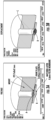
- Figs. 3A and 3B axisymmetric simulations of a single element bending mode transducer will be discussed.
- the transducers simulated in Figs. 3A and 3B were provided on a Macor mounting block with an optional acoustic matching layer. It is noted that the benefit (increased velocity factor) provided by the matching layer for embodiments of the present inventive concept is less than with a conventional thickness mode transducer.
- Fig. 3A in the axisymmetric simulation of a single element bending mode transducer the shading indicates applied voltage light grey (A) illustrates +5V and dark grey (B) illustrates -5V.
- Fig. 3B illustrates axial velocity, where dark grey (C) is stationary and light grey (D) is moving downwards.
- Fig. 4 illustrates a graph of velocity vs. frequency showing simulations with (upper trace) and without (lower trace) the optional matching layer.
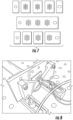
- FIGs. 5 through 7 illustrate the various processing steps in the fabrication of transducers in accordance with some embodiments discussed herein.
- Figs. 5 and 6 illustrate the PZT chips (7x8x0.1mm) bonded to a stainless steel substrates and subsequently laser-patterned.
- the square spaces at the sides illustrate electrical contact points 520 as discussed above.
- These electrical contact points 520 may include means for connecting the transducers, for example, spring contacts or metalized tracks to make electrical contact.
- Fig. 7 further illustrates the mounting block bonded to PZT-substrate assembly and subsequently singulated.
- FIGs. 8 and 9 illustrate the mechanical positioning of the transducers in a transducer mount ( Fig. 8 ) and included in a transmit and receive test fixture ( Fig. 9 ). Details of the testing will now be discussed and are illustrated in the table of Fig. 10 and graphs of Figs. 11-14 .
- Transducers in accordance with embodiments of the present inventive concept were mounted to a test fixture ( Fig. 9 ) with electrical contact via spring probes (RS Stock No. 261-5092) contacting in the electrode contact area away from the vibrating part of the transducer.
- the gain setting on the microphone preamplifier was set to a minimum value for low frequency tests and set to an intermediate value (gain control rotated 180 degrees) for high frequency tests.
- Transmit-receive performance was measured by selecting a pair of transducers connected by an acrylic tube ( Fig. 9 ) ID 18mm and length 15cm (for low frequency tests) and length 8.5cm (for high frequency tests).
- a digital oscilloscope was used to capture outputs from laser vibrometer, ultrasonic microphone and transducer transmit-receive tests.
- Figs. 11 and 12 are graphs illustrating electrical impedance spectra and oscilloscope traces showing vibrometer motion, acoustic output and transmit-receive burst response.
- Fig. 11 illustrates an electrical impedance spectra for low frequency transducers (device 11763A) and Fig. 12 illustrates electrical impedance spectra for high frequency transducers (device 11757A).
- Figs. 13 and 14 are graphs illustrating a microphone response in accordance with embodiments of the present inventive concept.
- the upper trace illustrates a drive signal of a low frequency transducer and the lower trace illustrates a microphone output of the low frequency transducer, device A11761C.
- the upper trace illustrates a drive signal of a low frequency transducer and the lower trace illustrates a receive transducer output of the low frequency transducer, device A11763A and A11763C.
- Transducers in accordance with embodiments discussed herein may be used in any device which lends itself to such transducer.
- these transducers may be used in water meters, gas meters and the like.
- transducers may be used in gas meters as illustrated in Fig. 15 .
- the gas meter 1500 includes three transducers.
- Transducer 1 (upstream) and transducer 2 (downstream) may be used to measure time-of-flight of an ultrasonic signal along the flow tube 1510 in forward and reverse directions.
- the gas meter 1500 may also be configured to compensate for gas properties and conditions using a separate sound measurement using transducer 3.
- Fig. 15 is provided for example only and embodiments of the present inventive concept are not limited to this configuration.
- Transducers as discussed herein may be used in many different devices.
- Example embodiments are described above with reference to block diagrams and/or flowchart illustrations of systems and devices.
- the functions/acts noted in the blocks may occur out of the order noted in the flowcharts.
- two blocks shown in succession may in fact be executed substantially concurrently or the blocks may sometimes be executed in the reverse order, depending upon the functionality/acts involved.
- the functionality of a given block of the flowcharts and/or block diagrams may be separated into multiple blocks and/or the functionality of two or more blocks of the flowcharts and/or block diagrams may be at least partially integrated.
Landscapes
- Engineering & Computer Science (AREA)
- Mechanical Engineering (AREA)
- Physics & Mathematics (AREA)
- Acoustics & Sound (AREA)
- General Engineering & Computer Science (AREA)
- Manufacturing & Machinery (AREA)
- Signal Processing (AREA)
- Multimedia (AREA)
- Investigating Or Analyzing Materials By The Use Of Ultrasonic Waves (AREA)
- Transducers For Ultrasonic Waves (AREA)
Claims (14)
- Biegungsmodenwandler (105) umfassend:ein Substrat (100), welches eine erste Fläche und eine zweite Fläche aufweist, welche der ersten Fläche entgegengesetzt ist;eine piezoelektrische Schicht (140) an der ersten Fläche des Substrats (100), wobei die piezoelektrische Schicht (140) ein PZT-Material umfasst und eine Dicke von in etwa 20 µm bis in etwa 1000 µm aufweist;wenigstens eine strukturierte Elektrode an der piezoelektrischen Schicht;einen Befestigungsblock (130) an der wenigstens einen strukturierten Elektrode, wobei der Befestigungsblock eine Dicke von 0,5 mm bis 10,0 mm aufweist; undwenigstens zwei elektrische Kontaktpunkte (120) an der wenigstens einen strukturierten Elektrode.
- Wandler (105) nach Anspruch 1, ferner umfassend Ausrichtungsmerkmale an dem Substrat (100) und/oder dem Befestigungsblock (130), um ein Ausrichten während eines Herstellungsprozesses zu unterstützen.
- Wandler (105) nach Anspruch 2, wobei die Ausrichtungsmerkmale eine Mehrzahl von Löchern und Schlitzen in dem Substrat (100) und/oder dem Befestigungsblock (130) umfassen.
- Wandler (105) nach Anspruch 1, wobei das Substrat (100) Edelstahl umfasst und eine Dicke von in etwa 10 µm bis in etwa 500 µm aufweist.
- Wandler (105) nach Anspruch 1, wobei der Befestigungsblock (130) eines aus einem keramischen Material und einem elektrisch isolierenden Material umfasst.
- Wandler (105) nach Anspruch 1, ferner umfassend eine akustische Anpassungsschicht an der zweiten Fläche des Substrats (100).
- Wandler (105) nach Anspruch 1, wobei die wenigstens eine strukturierte Elektrode eine Mehrzahl von strukturierten Elektroden umfasst.
- Wandler (105) nach Anspruch 1, wobei der Wandler (105) ein Ultraschallwandler ist, welcher für eines aus einem Gasmessgerät, einem Wassermessgerät und einem Wärmemessgerät eingerichtet ist.
- Vorrichtung umfassend wenigstens einen der Wandler (105) nach Anspruch 1.
- Verfahren zum Herstellen von Biegungsmodenwandlern (105), umfassend:Bereitstellen eines Substrats (100) umfassend ein Material mit hoher Dichte, wobei das Substrat (100) eine erste Fläche und eine zweite Fläche aufweist, welche der ersten Fläche entgegengesetzt ist;Verbinden einer piezoelektrischen Schicht (140) und von Elektroden an die erste Fläche des Substrats;Strukturieren der Elektroden, um wenigstens eine strukturierte Elektrode an der piezoelektrischen Schicht (140) bereitzustellen, wobei ein Laserabtragungsprozess verwendet wird; undVerbinden eines Befestigungsblocks (130) an der piezoelektrischen Schicht (140) und der wenigstens einen strukturierten Elektrode, wobei der Befestigungsblock eine Dicke von 0,5 mm bis 10,0 mm aufweist.
- Verfahren nach Anspruch 10, wobei die Elektroden eines aus Gold, Nickel und Silber umfassen.
- Verfahren nach Anspruch 10, wobei das Verbinden der piezoelektrischen Schicht (140) und der Elektroden ferner umfasst:Auftragen eines Klebstoffs an einer Fläche des Substrats (100) und/oder der piezoelektrischen Schicht (140);Zusammenpressen des Substrats (100) und der piezoelektrischen Schicht (140) umfassend die wenigstens eine strukturierte Elektrode; undAushärten des Klebstoffs derart, dass das Substrat (100) und die piezoelektrische Schicht (140) verbunden werden.
- Verfahren nach Anspruch 12, wobei das Aushärten durch ein Ausrichten des Substrats (100) mit dem Befestigungsblock (130) gefolgt ist, wobei Ausrichtungsmerkmale an dem Substrat (100) und/oder dem Befestigungsblock (130) verwendet werden, um ein Ausrichten während eines Verbindungsprozesses zu unterstützen, und wobei die Ausrichtungsmerkmale eine Mehrzahl von Löchern und Schlitzen in dem Substrat (100) und/oder der piezoelektrischen Schicht (140) umfassen.
- Verfahren nach Anspruch 10, wobei der Befestigungsblock (130) eines aus einem keramischen Material und einem elektrisch isolierenden Material umfasst.
Applications Claiming Priority (2)
| Application Number | Priority Date | Filing Date | Title |
|---|---|---|---|
| US201762461610P | 2017-02-21 | 2017-02-21 | |
| PCT/US2018/016604 WO2018156334A1 (en) | 2017-02-21 | 2018-02-02 | Multi-element bending transducers and related methods and devices |
Publications (3)
| Publication Number | Publication Date |
|---|---|
| EP3586331A1 EP3586331A1 (de) | 2020-01-01 |
| EP3586331B1 true EP3586331B1 (de) | 2025-04-09 |
| EP3586331C0 EP3586331C0 (de) | 2025-04-09 |
Family
ID=61249715
Family Applications (1)
| Application Number | Title | Priority Date | Filing Date |
|---|---|---|---|
| EP18706346.6A Active EP3586331B1 (de) | 2017-02-21 | 2018-02-02 | Mehrelement-biegewandler und zugehörige verfahren und vorrichtungen |
Country Status (5)
| Country | Link |
|---|---|
| US (1) | US11225961B2 (de) |
| EP (1) | EP3586331B1 (de) |
| CN (1) | CN110291580B (de) |
| CA (1) | CA3049836A1 (de) |
| WO (1) | WO2018156334A1 (de) |
Families Citing this family (4)
| Publication number | Priority date | Publication date | Assignee | Title |
|---|---|---|---|---|
| US10518293B2 (en) * | 2016-12-09 | 2019-12-31 | Sensus USA, Inc. | Thickness-planar mode transducers and related devices |
| US11225961B2 (en) * | 2017-02-21 | 2022-01-18 | Sensus Spectrum, Llc | Multi-element bending transducers and related methods and devices |
| EP3585526B1 (de) | 2017-02-24 | 2024-10-09 | Sensus Spectrum, LLC | Ultraschallvorrichtungen mit akustisch angepassten regionen darin |
| EP3701257B1 (de) * | 2017-10-27 | 2024-03-20 | Westinghouse Electric Company Llc | Vorrichtung und verfahren zur verbesserten erkennung von korrosionsverdünnung |
Citations (1)
| Publication number | Priority date | Publication date | Assignee | Title |
|---|---|---|---|---|
| US20160107194A1 (en) * | 2014-10-15 | 2016-04-21 | Qualcomm Incorporated | Three-port piezoelectric ultrasonic transducer |
Family Cites Families (20)
| Publication number | Priority date | Publication date | Assignee | Title |
|---|---|---|---|---|
| DE3069001D1 (en) * | 1979-05-16 | 1984-09-27 | Toray Industries | Piezoelectric vibration transducer |
| EP0119855B2 (de) | 1983-03-17 | 1992-06-10 | Matsushita Electric Industrial Co., Ltd. | Ultraschallwandler mit akustischen Impedanzanpassungsschichten |
| JPS61161446A (ja) * | 1985-01-10 | 1986-07-22 | Terumo Corp | 超音波探触子およびその製造方法 |
| US5295487A (en) * | 1992-02-12 | 1994-03-22 | Kabushiki Kaisha Toshiba | Ultrasonic probe |
| US5423220A (en) * | 1993-01-29 | 1995-06-13 | Parallel Design | Ultrasonic transducer array and manufacturing method thereof |
| US5539965A (en) * | 1994-06-22 | 1996-07-30 | Rutgers, The University Of New Jersey | Method for making piezoelectric composites |
| US5920972A (en) * | 1997-06-27 | 1999-07-13 | Siemens Medical Systems, Inc. | Interconnection method for a multilayer transducer array |
| JP3611198B2 (ja) * | 2000-02-16 | 2005-01-19 | 松下電器産業株式会社 | アクチュエータとこれを用いた情報記録再生装置 |
| US7181977B2 (en) | 2002-01-22 | 2007-02-27 | Measurement Specialties, Inc. | Sensor assembly with lead attachment |
| KR20040086504A (ko) | 2002-01-28 | 2004-10-11 | 마츠시타 덴끼 산교 가부시키가이샤 | 음향 정합층, 초음파 송수파기 및 이들의 제조 방법, 및초음파 유량계 |
| JP4473532B2 (ja) | 2002-10-10 | 2010-06-02 | 日本碍子株式会社 | 圧電/電歪デバイス及び製造方法 |
| US7247269B2 (en) * | 2003-07-21 | 2007-07-24 | Biosense Webster, Inc. | Method for making a spiral array ultrasound transducer |
| US20060169055A1 (en) | 2005-01-06 | 2006-08-03 | Sensotech | Method and system for measuring fluid level in a container |
| US9184369B2 (en) * | 2008-09-18 | 2015-11-10 | Fujifilm Sonosite, Inc. | Methods for manufacturing ultrasound transducers and other components |
| JP5954773B2 (ja) * | 2012-03-13 | 2016-07-20 | 東芝メディカルシステムズ株式会社 | 超音波プローブおよび超音波プローブの製造方法 |
| US20140184023A1 (en) | 2012-12-31 | 2014-07-03 | Volcano Corporation | Layout and Method of Singulating Miniature Ultrasonic Transducers |
| US9603580B2 (en) * | 2013-05-24 | 2017-03-28 | Fujifilm Sonosite, Inc. | High frequency ultrasound probe |
| JP6233164B2 (ja) | 2014-04-15 | 2017-11-22 | 株式会社デンソー | 圧電素子、及び、光走査装置 |
| DK3237121T3 (da) * | 2014-12-23 | 2019-11-25 | Meggitt As | Fremgangsmåde til fremstilling af integrerede akustiske multielement-transducere |
| US11225961B2 (en) * | 2017-02-21 | 2022-01-18 | Sensus Spectrum, Llc | Multi-element bending transducers and related methods and devices |
-
2018
- 2018-02-02 US US15/887,065 patent/US11225961B2/en active Active
- 2018-02-02 EP EP18706346.6A patent/EP3586331B1/de active Active
- 2018-02-02 WO PCT/US2018/016604 patent/WO2018156334A1/en not_active Ceased
- 2018-02-02 CN CN201880013043.XA patent/CN110291580B/zh active Active
- 2018-02-02 CA CA3049836A patent/CA3049836A1/en active Pending
Patent Citations (1)
| Publication number | Priority date | Publication date | Assignee | Title |
|---|---|---|---|---|
| US20160107194A1 (en) * | 2014-10-15 | 2016-04-21 | Qualcomm Incorporated | Three-port piezoelectric ultrasonic transducer |
Also Published As
| Publication number | Publication date |
|---|---|
| US20180242066A1 (en) | 2018-08-23 |
| US11225961B2 (en) | 2022-01-18 |
| EP3586331A1 (de) | 2020-01-01 |
| CA3049836A1 (en) | 2018-08-30 |
| CN110291580B (zh) | 2024-02-20 |
| CN110291580A (zh) | 2019-09-27 |
| EP3586331C0 (de) | 2025-04-09 |
| WO2018156334A1 (en) | 2018-08-30 |
Similar Documents
| Publication | Publication Date | Title |
|---|---|---|
| US7471034B2 (en) | Ultrasound transducer and method of producing the same | |
| EP3586331B1 (de) | Mehrelement-biegewandler und zugehörige verfahren und vorrichtungen | |
| US6323661B1 (en) | Measurement of printed circuit-to-conductive substrate contact resistance | |
| CN111147989A (zh) | 具有用于多维换能器阵列的中介层的阵列上芯片 | |
| Oppenheim et al. | MEMS ultrasonic transducers for the testing of solids | |
| US5724315A (en) | Omnidirectional ultrasonic microprobe hydrophone | |
| US20240416386A1 (en) | Ultrasound interconnect stack and method of manufacturing same | |
| EP3551349B1 (de) | Dicken-/planarmoduswandler und zugehörige vorrichtungen | |
| Hu et al. | Unclosed Hexagonal Piezoelectric MEMS Hydrophone Based on Rigid-Flexible Composite Membrane | |
| CN110087783B (zh) | 厚度模式传感器和相关设备及方法 | |
| JP2017148258A (ja) | 超音波探触子とその製造方法ならびに超音波診断装置 | |
| CN220289503U (zh) | 核电厂相控阵探头 | |
| CN118692434B (zh) | 一种宽频带水声换能器基阵 | |
| Frankenstein et al. | Monitoring Network for SHM in avionic applications | |
| CN118541009A (zh) | 一种高可靠压电复合元件及其制备方法 | |
| Chang et al. | Design and Implementation of PZT Piezoelectric Micromachined Ultrasonic Transducers for Distance Sensing | |
| Yu et al. | Highly Consistent, Miniaturized Transverse Wave Ultrasonic Transducer Array Based on 147° Orientation in X-Cut Lithium Niobate for High Resolution Imaging | |
| Stoeckel et al. | Technology for Piezoelectric Micromachined Ultrasonic Transducers with Adaptive Channel Geometry and Chip Size | |
| Gottlieb et al. | High frequency copolymer annular array ultrasound transducer fabrication technology | |
| Porchez et al. | Piezo-composite patches applied to the detection of defects using Lamb wave focusing | |
| Moffett | Omnidirectional Ultrasonic Microprobe Hydrophone. |
Legal Events
| Date | Code | Title | Description |
|---|---|---|---|
| STAA | Information on the status of an ep patent application or granted ep patent |
Free format text: STATUS: UNKNOWN |
|
| STAA | Information on the status of an ep patent application or granted ep patent |
Free format text: STATUS: THE INTERNATIONAL PUBLICATION HAS BEEN MADE |
|
| PUAI | Public reference made under article 153(3) epc to a published international application that has entered the european phase |
Free format text: ORIGINAL CODE: 0009012 |
|
| STAA | Information on the status of an ep patent application or granted ep patent |
Free format text: STATUS: REQUEST FOR EXAMINATION WAS MADE |
|
| 17P | Request for examination filed |
Effective date: 20190815 |
|
| AK | Designated contracting states |
Kind code of ref document: A1 Designated state(s): AL AT BE BG CH CY CZ DE DK EE ES FI FR GB GR HR HU IE IS IT LI LT LU LV MC MK MT NL NO PL PT RO RS SE SI SK SM TR |
|
| AX | Request for extension of the european patent |
Extension state: BA ME |
|
| DAV | Request for validation of the european patent (deleted) | ||
| DAX | Request for extension of the european patent (deleted) | ||
| STAA | Information on the status of an ep patent application or granted ep patent |
Free format text: STATUS: EXAMINATION IS IN PROGRESS |
|
| 17Q | First examination report despatched |
Effective date: 20210809 |
|
| GRAP | Despatch of communication of intention to grant a patent |
Free format text: ORIGINAL CODE: EPIDOSNIGR1 |
|
| STAA | Information on the status of an ep patent application or granted ep patent |
Free format text: STATUS: GRANT OF PATENT IS INTENDED |
|
| RIC1 | Information provided on ipc code assigned before grant |
Ipc: H04R 17/00 20060101ALI20240917BHEP Ipc: G10K 11/00 20060101AFI20240917BHEP |
|
| INTG | Intention to grant announced |
Effective date: 20241008 |
|
| GRAS | Grant fee paid |
Free format text: ORIGINAL CODE: EPIDOSNIGR3 |
|
| GRAA | (expected) grant |
Free format text: ORIGINAL CODE: 0009210 |
|
| STAA | Information on the status of an ep patent application or granted ep patent |
Free format text: STATUS: THE PATENT HAS BEEN GRANTED |
|
| AK | Designated contracting states |
Kind code of ref document: B1 Designated state(s): AL AT BE BG CH CY CZ DE DK EE ES FI FR GB GR HR HU IE IS IT LI LT LU LV MC MK MT NL NO PL PT RO RS SE SI SK SM TR |
|
| REG | Reference to a national code |
Ref country code: GB Ref legal event code: FG4D |
|
| REG | Reference to a national code |
Ref country code: CH Ref legal event code: EP |
|
| REG | Reference to a national code |
Ref country code: DE Ref legal event code: R096 Ref document number: 602018080919 Country of ref document: DE |
|
| REG | Reference to a national code |
Ref country code: IE Ref legal event code: FG4D |
|
| U01 | Request for unitary effect filed |
Effective date: 20250409 |
|
| U07 | Unitary effect registered |
Designated state(s): AT BE BG DE DK EE FI FR IT LT LU LV MT NL PT RO SE SI Effective date: 20250416 |
|
| PG25 | Lapsed in a contracting state [announced via postgrant information from national office to epo] |
Ref country code: ES Free format text: LAPSE BECAUSE OF FAILURE TO SUBMIT A TRANSLATION OF THE DESCRIPTION OR TO PAY THE FEE WITHIN THE PRESCRIBED TIME-LIMIT Effective date: 20250409 |
|
| PG25 | Lapsed in a contracting state [announced via postgrant information from national office to epo] |
Ref country code: NO Free format text: LAPSE BECAUSE OF FAILURE TO SUBMIT A TRANSLATION OF THE DESCRIPTION OR TO PAY THE FEE WITHIN THE PRESCRIBED TIME-LIMIT Effective date: 20250709 Ref country code: GR Free format text: LAPSE BECAUSE OF FAILURE TO SUBMIT A TRANSLATION OF THE DESCRIPTION OR TO PAY THE FEE WITHIN THE PRESCRIBED TIME-LIMIT Effective date: 20250710 |
|
| PG25 | Lapsed in a contracting state [announced via postgrant information from national office to epo] |
Ref country code: PL Free format text: LAPSE BECAUSE OF FAILURE TO SUBMIT A TRANSLATION OF THE DESCRIPTION OR TO PAY THE FEE WITHIN THE PRESCRIBED TIME-LIMIT Effective date: 20250409 |
|
| PG25 | Lapsed in a contracting state [announced via postgrant information from national office to epo] |
Ref country code: HR Free format text: LAPSE BECAUSE OF FAILURE TO SUBMIT A TRANSLATION OF THE DESCRIPTION OR TO PAY THE FEE WITHIN THE PRESCRIBED TIME-LIMIT Effective date: 20250409 |
|
| PG25 | Lapsed in a contracting state [announced via postgrant information from national office to epo] |
Ref country code: RS Free format text: LAPSE BECAUSE OF FAILURE TO SUBMIT A TRANSLATION OF THE DESCRIPTION OR TO PAY THE FEE WITHIN THE PRESCRIBED TIME-LIMIT Effective date: 20250709 |
|
| PG25 | Lapsed in a contracting state [announced via postgrant information from national office to epo] |
Ref country code: IS Free format text: LAPSE BECAUSE OF FAILURE TO SUBMIT A TRANSLATION OF THE DESCRIPTION OR TO PAY THE FEE WITHIN THE PRESCRIBED TIME-LIMIT Effective date: 20250809 |
|
| PG25 | Lapsed in a contracting state [announced via postgrant information from national office to epo] |
Ref country code: SM Free format text: LAPSE BECAUSE OF FAILURE TO SUBMIT A TRANSLATION OF THE DESCRIPTION OR TO PAY THE FEE WITHIN THE PRESCRIBED TIME-LIMIT Effective date: 20250409 |
|
| PG25 | Lapsed in a contracting state [announced via postgrant information from national office to epo] |
Ref country code: CZ Free format text: LAPSE BECAUSE OF FAILURE TO SUBMIT A TRANSLATION OF THE DESCRIPTION OR TO PAY THE FEE WITHIN THE PRESCRIBED TIME-LIMIT Effective date: 20250409 |
|
| PG25 | Lapsed in a contracting state [announced via postgrant information from national office to epo] |
Ref country code: SK Free format text: LAPSE BECAUSE OF FAILURE TO SUBMIT A TRANSLATION OF THE DESCRIPTION OR TO PAY THE FEE WITHIN THE PRESCRIBED TIME-LIMIT Effective date: 20250409 |
|
| PLBE | No opposition filed within time limit |
Free format text: ORIGINAL CODE: 0009261 |
|
| STAA | Information on the status of an ep patent application or granted ep patent |
Free format text: STATUS: NO OPPOSITION FILED WITHIN TIME LIMIT |
|
| REG | Reference to a national code |
Ref country code: CH Ref legal event code: L10 Free format text: ST27 STATUS EVENT CODE: U-0-0-L10-L00 (AS PROVIDED BY THE NATIONAL OFFICE) Effective date: 20260218 |
|
| 26N | No opposition filed |
Effective date: 20260112 |
|
| U20 | Renewal fee for the european patent with unitary effect paid |
Year of fee payment: 9 Effective date: 20260227 |
|
| PGFP | Annual fee paid to national office [announced via postgrant information from national office to epo] |
Ref country code: GB Payment date: 20260227 Year of fee payment: 9 |