EP3584904B1 - Intelligent wearable device with charger - Google Patents
Intelligent wearable device with charger Download PDFInfo
- Publication number
- EP3584904B1 EP3584904B1 EP17896794.9A EP17896794A EP3584904B1 EP 3584904 B1 EP3584904 B1 EP 3584904B1 EP 17896794 A EP17896794 A EP 17896794A EP 3584904 B1 EP3584904 B1 EP 3584904B1
- Authority
- EP
- European Patent Office
- Prior art keywords
- wearable device
- smart wearable
- open slot
- case
- slot
- Prior art date
- Legal status (The legal status is an assumption and is not a legal conclusion. Google has not performed a legal analysis and makes no representation as to the accuracy of the status listed.)
- Active
Links
- 239000002184 metal Substances 0.000 claims description 16
- 239000004743 Polypropylene Substances 0.000 claims description 3
- 239000013013 elastic material Substances 0.000 claims description 3
- 239000004033 plastic Substances 0.000 claims description 3
- -1 polypropylene Polymers 0.000 claims description 3
- 229920001155 polypropylene Polymers 0.000 claims description 3
- 238000000034 method Methods 0.000 description 10
- 238000005452 bending Methods 0.000 description 7
- 230000004308 accommodation Effects 0.000 description 3
- 238000010586 diagram Methods 0.000 description 3
- ZMHWQAHZKUPENF-UHFFFAOYSA-N 1,2-dichloro-3-(4-chlorophenyl)benzene Chemical compound C1=CC(Cl)=CC=C1C1=CC=CC(Cl)=C1Cl ZMHWQAHZKUPENF-UHFFFAOYSA-N 0.000 description 2
- ZGHQUYZPMWMLBM-UHFFFAOYSA-N 1,2-dichloro-4-phenylbenzene Chemical compound C1=C(Cl)C(Cl)=CC=C1C1=CC=CC=C1 ZGHQUYZPMWMLBM-UHFFFAOYSA-N 0.000 description 2
- 230000000694 effects Effects 0.000 description 2
- 238000000354 decomposition reaction Methods 0.000 description 1
- 238000012966 insertion method Methods 0.000 description 1
- 239000000463 material Substances 0.000 description 1
Images
Classifications
-
- H—ELECTRICITY
- H02—GENERATION; CONVERSION OR DISTRIBUTION OF ELECTRIC POWER
- H02J—CIRCUIT ARRANGEMENTS OR SYSTEMS FOR SUPPLYING OR DISTRIBUTING ELECTRIC POWER; SYSTEMS FOR STORING ELECTRIC ENERGY
- H02J7/00—Circuit arrangements for charging or depolarising batteries or for supplying loads from batteries
- H02J7/0042—Circuit arrangements for charging or depolarising batteries or for supplying loads from batteries characterised by the mechanical construction
- H02J7/0044—Circuit arrangements for charging or depolarising batteries or for supplying loads from batteries characterised by the mechanical construction specially adapted for holding portable devices containing batteries
-
- H—ELECTRICITY
- H01—ELECTRIC ELEMENTS
- H01R—ELECTRICALLY-CONDUCTIVE CONNECTIONS; STRUCTURAL ASSOCIATIONS OF A PLURALITY OF MUTUALLY-INSULATED ELECTRICAL CONNECTING ELEMENTS; COUPLING DEVICES; CURRENT COLLECTORS
- H01R13/00—Details of coupling devices of the kinds covered by groups H01R12/70 or H01R24/00 - H01R33/00
- H01R13/02—Contact members
- H01R13/22—Contacts for co-operating by abutting
- H01R13/24—Contacts for co-operating by abutting resilient; resiliently-mounted
- H01R13/2407—Contacts for co-operating by abutting resilient; resiliently-mounted characterized by the resilient means
- H01R13/2414—Contacts for co-operating by abutting resilient; resiliently-mounted characterized by the resilient means conductive elastomers
-
- H—ELECTRICITY
- H02—GENERATION; CONVERSION OR DISTRIBUTION OF ELECTRIC POWER
- H02J—CIRCUIT ARRANGEMENTS OR SYSTEMS FOR SUPPLYING OR DISTRIBUTING ELECTRIC POWER; SYSTEMS FOR STORING ELECTRIC ENERGY
- H02J7/00—Circuit arrangements for charging or depolarising batteries or for supplying loads from batteries
-
- H—ELECTRICITY
- H05—ELECTRIC TECHNIQUES NOT OTHERWISE PROVIDED FOR
- H05K—PRINTED CIRCUITS; CASINGS OR CONSTRUCTIONAL DETAILS OF ELECTRIC APPARATUS; MANUFACTURE OF ASSEMBLAGES OF ELECTRICAL COMPONENTS
- H05K7/00—Constructional details common to different types of electric apparatus
- H05K7/14—Mounting supporting structure in casing or on frame or rack
- H05K7/1422—Printed circuit boards receptacles, e.g. stacked structures, electronic circuit modules or box like frames
- H05K7/1427—Housings
-
- H—ELECTRICITY
- H01—ELECTRIC ELEMENTS
- H01R—ELECTRICALLY-CONDUCTIVE CONNECTIONS; STRUCTURAL ASSOCIATIONS OF A PLURALITY OF MUTUALLY-INSULATED ELECTRICAL CONNECTING ELEMENTS; COUPLING DEVICES; CURRENT COLLECTORS
- H01R13/00—Details of coupling devices of the kinds covered by groups H01R12/70 or H01R24/00 - H01R33/00
- H01R13/02—Contact members
- H01R13/22—Contacts for co-operating by abutting
- H01R13/24—Contacts for co-operating by abutting resilient; resiliently-mounted
- H01R13/2407—Contacts for co-operating by abutting resilient; resiliently-mounted characterized by the resilient means
- H01R13/2421—Contacts for co-operating by abutting resilient; resiliently-mounted characterized by the resilient means using coil springs
Definitions
- the present disclosure relates to a system comprising a smart wearable device and a charger thereof.
- connection methods between the smart wearable devices in the related art and their charging bases are versatile.
- a wireless method, a snap-fit method, a magnetic attraction method, and the like are used to connect so as to perform charging.
- the wireless method has flexibility and charging can be realized without a physical connection to the smart wearable device.
- the snap-fit method achieves a stable connection.
- the magnetic attraction method achieves a more accurate connection.
- these various methods all have a same problem, that is, the structure is complex. As a result, the service life can not be guaranteed and the cost is high.
- Document US2016/02177A1 discloses a main body (100) of a wearable device.
- the main body (100) of the wearable device includes a front case (110), a bottom case (130) joined with the front case (110) to form a waterproof cavity, and electronic components (150) disposed in the cavity.
- the electronic components include a printed circuit board (PCB)(151) and a battery (152) electrically connected to each other.
- the PCB (151) has a wireless data transceiving assembly and at least one sensor.
- the bottom case (130) includes two charging contacts (131) formed on an outer side of the bottom case (130) and electrically coupled to the electronic components (150).
- the present invention provides a system according to claim 1.
- the present disclosure provides a system comprising a smart wearable device and a charger thereof.
- the connection structure is simple, the connection is stable, and the cost is low.
- the present invention provides a smart wearable device and a charging base configured to charge the smart wearable device.
- the charging base comprises an elastic case.
- An open slot for inserting the smart wearable device is formed in the case.
- a power supply portion is disposed on the charging base.
- the power supply portion provides the smart wearable device with electrical energy for charging.
- the smart wearable device is fixed to the charging base by way of a close fit between slot walls on two sides of the open slot and an outer surface of the smart wearable device.
- cross sections of the slot walls on two sides of the open slot are concave curves
- cross sections of the outer surface of the smart wearable device opposite to the slot walls on two sides of the open slot are convex curves to form joint portions
- a radian of the joint portions is equal to a radian of the slot walls on two sides of the open slot.
- a depth of the open slot is greater than one half of a thickness of the smart wearable device.
- the power supply portion comprises a first printed circuit board (PCB) disposed in the case for charging.
- a pogo pin is connected to the first PCB.
- a spring hole for extension of ends of pin shafts of the pogo pin is formed in the case located on a bottom of the open slot.
- the pin shafts of the pogo pin extend into the open slot from the spring hole.
- Metal pillars that are in contact with elastic pieces on a second PCB of the smart wearable device are disposed in the smart wearable device. Pillar holes are formed in one side of an outer surface of the smart wearable device opposite to the bottom of the open slot. Positions of the pillar holes correspond to positions of the metal pillars. One end of each of the metal pillars away from the elastic piece is inserted into the pillar hole.
- the pin shafts of the pogo pin and end surfaces of the metal pillars away from the elastic pieces are brought into contact to conduct after the smart wearable device is inserted into the open slot so as to charge the smart wearable device.
- a circumferential protruding portion is disposed at an upper end of the pogo pin.
- the protruding portion surrounds the pin shafts of the pogo pin.
- a shape and a size of the spring hole are adapted to a shape and a size of the protruding portion.
- Matching grooves are formed in the one side of the outer surface of the smart wearable device opposite to the bottom of the open slot and are located where the pillar holes are located.
- the matching grooves are adaptively connected to the protruding portion, the end surfaces of the metal pillars away from the elastic pieces extend into the matching grooves from the pillar holes.
- a deformation slot is formed on another side of the case opposite to the open slot. Disposition directions of the deformation slot and the open slot are the same.
- a supporting skeleton is disposed in the case.
- the case is made of a thermal plastic and elastic material.
- the case is made of polypropylene.
- the present disclosure disposes a charging base having an open slot and having elasticity.
- the insertion method is adopted to allow the slot walls of the open slot and the outer surface of the smart wearable device to closely contact so as to achieve connection.
- a friction force is thus formed between the slot walls and the outer surface of the smart wearable device.
- the smart wearable device can be fixed to the charging base to perform charging. Not only is the reliable connection achieved, but the structure is also simple and the cost is also low.
- a smart wearable device and a charger thereof comprises a smart wearable device 1 and a charging base 2 configured to charge the smart wearable device 1.
- the charging base 2 has a power supply portion for supplying power to the smart wearable device 1.
- the power supply portion and a connection portion for matching the smart wearable device 1 and the power supply portion may be implemented by using a common charging port in the related art.
- the improvement of the present disclosure lies in the connection method between the smart wearable device 1 and the charging base 2.
- the charging base 2 comprises an elastic case 21.
- the elastic case 21 is made of a material with more friction.
- An open slot 212 for inserting the smart wearable device 1 is formed in an upper surface of the case 21.
- a depth of the open slot 212 is greater than one half of a thickness of the smart wearable device 1. Through adjusting the depth of the open slot 212, a clamping force and a friction force of the open slot 212 can be adjusted to increase the fastness.
- the power supply portion is disposed on the charging base 2.
- the power supply portion provides the smart wearable device 1 with electrical energy for charging.
- the smart wearable device 1 is fixed to the charging base 2 by way of a close fit between slot walls on two sides of the open slot 212 and an outer surface of the smart wearable device 1.
- cross sections of the slot walls on two sides of the open slot 212 are concave curves to form a shape similar to a paw. In this manner, the fastness can be increased.
- cross sections of the outer surface of the smart wearable device 1 opposite to the slot walls on two sides of the open slot 212 are convex curves to form joint portions.
- a radian of the joint portions 11 is equal to a radian of the slot walls on two sides of the open slot 212.
- the power supply portion in the present disclosure may be realized by using the structure as follows.
- the structure comprises a first printed circuit board (PCB) 22 disposed in the case 21 for charging.
- a pogo pin 23 is connected to the first PCB 22.
- a spring hole 213 for extension of ends of pin shafts of the pogo pin 23 is formed in the case 21 located on a bottom of the open slot 212. The pin shafts of the pogo pin 23 extend into the open slot 212 from the spring hole 213.
- Pillar holes 15 are formed in one side of the outer surface of the smart wearable device 1 opposite to the bottom of the open slot 212. Positions of the pillar holes 15 correspond to positions of the metal pillars 14. One end of each of the metal pillars 14 away from elastic piece 13 is inserted into the pillar hole 15.
- the pin shafts of the pogo pin 23 and end surfaces of the metal pillars 14 away from elastic pieces 13 are brought into contact to conduct after the smart wearable device 1 is inserted into the open slot 212. As a result, the smart wearable device 1 is charged.
- a circumferential protruding portion 24 is disposed at an upper end of the pogo pin 23.
- the protruding portion 24 surrounds the pin shafts of the pogo pin 23.
- a shape and a size of the spring hole 213 are adapted to a shape and a size of the protruding portion 24.
- Matching grooves 16 are formed in the one side of the outer surface of the smart wearable device 1 opposite to the bottom of the open slot 212 and are located where the pillar holes 15 are located.
- the matching grooves 16 are adaptively connected to the protruding portion 24.
- the end surfaces of the metal pillars 14 away from elastic pieces 13 extend into the matching grooves 16 from the pillar holes 15.
- the smart wearable device 1 further comprises an upper case 3 and a lower case 4 disposed underneath the upper case 3.
- An accommodation space for placing the second PCB 12 is formed in the upper case 3.
- Functional components required by the smart wearable device 1, such as a battery, etc., may further be place in the accommodation space, but the present disclosure is not limited in this regard.
- the pillar holes 15 and the matching grooves 16 are all formed in the lower case 4.
- the lower case 4 and the upper case 3 are connected through hooks so as to close the accommodation space in the upper case 3.
- the joint portions 11 are disposed on the upper case 3.
- the pogo pin 23 is disposed on one side of the open slot 212 close to an edge of an opening of the open slot 212.
- a deformation slot 214 is formed on a bottom of the case 21 that is on another side of the case 21 opposite to the open slot 212. Disposition directions of the deformation slot 214 and the open slot 212 are the same. Opening of the open slot 212 can be easier when the smart wearable device 1 is placed into the open slot 212 of the charging base 2.
- a depth of the deformation slot 214 is less than the depth of the open slot 212.
- the depth of the deformation slot 214 is one half of the depth of the open slot 212.
- a supporting skeleton 211 is disposed in the case 21.
- a shape of the supporting skeleton 211 is similar to a shape of the case 21.
- a groove 2111 for fixing the pogo pin 23 and the first PCB 22 is formed in the supporting skeleton 211 corresponding to a position of the pogo pin 23.
- first bending portions 215 are respectively disposed at two ends of each of the slot walls on two sides of the open slot 212.
- Second bending portions 31 are disposed on the upper case 3 of the smart wearable device 1 corresponding to positions of the first bending portions 215.
- the case 21 is made of a thermal plastic and elastic material having considerable elasticity and flexibility.
- the supporting skeleton 211 is made of polypropylene.
- the joint portions 11 of the smart wearable device 1 are aligned with the open slot 212 and are pushed into the open slot 212 hard when charging, so that the slot walls on two sides of the open slot 212 deform and flare.
- the first bending portions 215 at the two ends of each of the slot walls on two sides of the open slot 212 and the second bending portions 31 have the guidance effect. After the smart wearable device 1 completely enters into the open slot 212, the slot walls on two sides of the open slot 212 restore and contact the joint portions 11.
- the guidance effect of the first bending portions 215 and the second bending portions 31 allows the matching grooves 16 of the smart wearable device 1 to successfully join with the protruding portion 24, and also brings the pin shafts of the pogo pin 23 and the metal pillars 14 into contact so as to conduct. As a result, the charging is performed.
- the smart wearable device 1 may be a smart bracelet, a smart watch, or the like.
Landscapes
- Engineering & Computer Science (AREA)
- Power Engineering (AREA)
- Microelectronics & Electronic Packaging (AREA)
- Charge And Discharge Circuits For Batteries Or The Like (AREA)
Description
- The present disclosure relates to a system comprising a smart wearable device and a charger thereof.
- With the increasing number of types of electronic devices, smart wearable devices have gradually become familiar to people. The connection methods between the smart wearable devices in the related art and their charging bases are versatile. For example, a wireless method, a snap-fit method, a magnetic attraction method, and the like are used to connect so as to perform charging. These various methods have their respective advantages. The wireless method has flexibility and charging can be realized without a physical connection to the smart wearable device. The snap-fit method achieves a stable connection. The magnetic attraction method achieves a more accurate connection. However, these various methods all have a same problem, that is, the structure is complex. As a result, the service life can not be guaranteed and the cost is high.
- Document
US2016/02177A1 discloses a main body (100) of a wearable device. The main body (100) of the wearable device includes a front case (110), a bottom case (130) joined with the front case (110) to form a waterproof cavity, and electronic components (150) disposed in the cavity. The electronic components include a printed circuit board (PCB)(151) and a battery (152) electrically connected to each other. The PCB (151) has a wireless data transceiving assembly and at least one sensor. The bottom case (130) includes two charging contacts (131) formed on an outer side of the bottom case (130) and electrically coupled to the electronic components (150). - The present invention provides a system according to
claim 1. The present disclosure provides a system comprising a smart wearable device and a charger thereof. As a result, the connection structure is simple, the connection is stable, and the cost is low. - The present invention provides a smart wearable device and a charging base configured to charge the smart wearable device. The charging base comprises an elastic case. An open slot for inserting the smart wearable device is formed in the case. A power supply portion is disposed on the charging base. The power supply portion provides the smart wearable device with electrical energy for charging. The smart wearable device is fixed to the charging base by way of a close fit between slot walls on two sides of the open slot and an outer surface of the smart wearable device.
- Furthermore, cross sections of the slot walls on two sides of the open slot are concave curves, cross sections of the outer surface of the smart wearable device opposite to the slot walls on two sides of the open slot are convex curves to form joint portions, a radian of the joint portions is equal to a radian of the slot walls on two sides of the open slot.
- According to an embodiment, a depth of the open slot is greater than one half of a thickness of the smart wearable device.
- Furthermore, the power supply portion comprises a first printed circuit board (PCB) disposed in the case for charging. A pogo pin is connected to the first PCB. A spring hole for extension of ends of pin shafts of the pogo pin is formed in the case located on a bottom of the open slot. The pin shafts of the pogo pin extend into the open slot from the spring hole. Metal pillars that are in contact with elastic pieces on a second PCB of the smart wearable device are disposed in the smart wearable device. Pillar holes are formed in one side of an outer surface of the smart wearable device opposite to the bottom of the open slot. Positions of the pillar holes correspond to positions of the metal pillars. One end of each of the metal pillars away from the elastic piece is inserted into the pillar hole. The pin shafts of the pogo pin and end surfaces of the metal pillars away from the elastic pieces are brought into contact to conduct after the smart wearable device is inserted into the open slot so as to charge the smart wearable device.
- According to an embodiment, a circumferential protruding portion is disposed at an upper end of the pogo pin. The protruding portion surrounds the pin shafts of the pogo pin. A shape and a size of the spring hole are adapted to a shape and a size of the protruding portion. Matching grooves are formed in the one side of the outer surface of the smart wearable device opposite to the bottom of the open slot and are located where the pillar holes are located. The matching grooves are adaptively connected to the protruding portion, the end surfaces of the metal pillars away from the elastic pieces extend into the matching grooves from the pillar holes.
- According to an embodiment, a deformation slot is formed on another side of the case opposite to the open slot. Disposition directions of the deformation slot and the open slot are the same.
- According to an embodiment, a supporting skeleton is disposed in the case.
- According to an embodiment, the case is made of a thermal plastic and elastic material.
- According to an embodiment, the case is made of polypropylene.
- As compared with the related art, the present disclosure disposes a charging base having an open slot and having elasticity. The insertion method is adopted to allow the slot walls of the open slot and the outer surface of the smart wearable device to closely contact so as to achieve connection. A friction force is thus formed between the slot walls and the outer surface of the smart wearable device. As a result, the smart wearable device can be fixed to the charging base to perform charging. Not only is the reliable connection achieved, but the structure is also simple and the cost is also low.
-
-
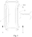
Fig. 1 is a schematic diagram of a connection structure of a smart wearable device according to the present disclosure. -
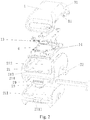
Fig. 2 is a schematic diagram of a three-dimensional decomposition structure according to the present disclosure. -
Fig. 3 is a cross-sectional view taken along line A-A ofFig. 1 . -
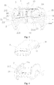
Fig. 4 is a schematic diagram of a service state of the present disclosure. - The invention is described below in detail with reference to the accompanying drawings, wherein like reference numerals are used to identify like elements illustrated in one or more of the figures thereof, and in which exemplary embodiments of the invention are shown.
- A description is provided with reference to
Fig. 1 ,Fig. 2 andFig. 3 . A smart wearable device and a charger thereof according to the present disclosure comprises a smartwearable device 1 and acharging base 2 configured to charge the smartwearable device 1. According to the present disclosure, thecharging base 2 has a power supply portion for supplying power to the smartwearable device 1. In addition, the power supply portion and a connection portion for matching the smartwearable device 1 and the power supply portion may be implemented by using a common charging port in the related art. The improvement of the present disclosure lies in the connection method between the smartwearable device 1 and the chargingbase 2. - The charging
base 2 comprises anelastic case 21. Theelastic case 21 is made of a material with more friction. Anopen slot 212 for inserting the smartwearable device 1 is formed in an upper surface of thecase 21. A depth of theopen slot 212 is greater than one half of a thickness of the smartwearable device 1. Through adjusting the depth of theopen slot 212, a clamping force and a friction force of theopen slot 212 can be adjusted to increase the fastness. The power supply portion is disposed on the chargingbase 2. The power supply portion provides the smartwearable device 1 with electrical energy for charging. The smartwearable device 1 is fixed to the chargingbase 2 by way of a close fit between slot walls on two sides of theopen slot 212 and an outer surface of the smartwearable device 1. - As shown in
Fig. 3 , cross sections of the slot walls on two sides of theopen slot 212 are concave curves to form a shape similar to a paw. In this manner, the fastness can be increased. Correspondingly, cross sections of the outer surface of the smartwearable device 1 opposite to the slot walls on two sides of theopen slot 212 are convex curves to form joint portions. A radian of thejoint portions 11 is equal to a radian of the slot walls on two sides of theopen slot 212. - The power supply portion in the present disclosure may be realized by using the structure as follows. The structure comprises a first printed circuit board (PCB) 22 disposed in the
case 21 for charging. Apogo pin 23 is connected to thefirst PCB 22. Aspring hole 213 for extension of ends of pin shafts of thepogo pin 23 is formed in thecase 21 located on a bottom of theopen slot 212. The pin shafts of thepogo pin 23 extend into theopen slot 212 from thespring hole 213. - As shown in
Fig. 2 andFig. 3 ,metal pillars 14 that are in contact withelastic pieces 13 on asecond PCB 12 of the smartwearable device 1 are disposed in the smartwearable device 1. Pillar holes 15 are formed in one side of the outer surface of the smartwearable device 1 opposite to the bottom of theopen slot 212. Positions of the pillar holes 15 correspond to positions of themetal pillars 14. One end of each of themetal pillars 14 away fromelastic piece 13 is inserted into thepillar hole 15. - When being connected, the pin shafts of the
pogo pin 23 and end surfaces of themetal pillars 14 away fromelastic pieces 13 are brought into contact to conduct after the smartwearable device 1 is inserted into theopen slot 212. As a result, the smartwearable device 1 is charged. - In order to avoid the mounting error of the smart
wearable device 1 and the chargingbase 2, acircumferential protruding portion 24 is disposed at an upper end of thepogo pin 23. The protrudingportion 24 surrounds the pin shafts of thepogo pin 23. A shape and a size of thespring hole 213 are adapted to a shape and a size of the protrudingportion 24. Matchinggrooves 16 are formed in the one side of the outer surface of the smartwearable device 1 opposite to the bottom of theopen slot 212 and are located where the pillar holes 15 are located. The matchinggrooves 16 are adaptively connected to the protrudingportion 24. The end surfaces of themetal pillars 14 away fromelastic pieces 13 extend into the matchinggrooves 16 from the pillar holes 15. - The smart
wearable device 1 further comprises anupper case 3 and alower case 4 disposed underneath theupper case 3. An accommodation space for placing thesecond PCB 12 is formed in theupper case 3. Functional components required by the smartwearable device 1, such as a battery, etc., may further be place in the accommodation space, but the present disclosure is not limited in this regard. The pillar holes 15 and the matchinggrooves 16 are all formed in thelower case 4. Thelower case 4 and theupper case 3 are connected through hooks so as to close the accommodation space in theupper case 3. Thejoint portions 11 are disposed on theupper case 3. - According to the present disclosure, the
pogo pin 23 is disposed on one side of theopen slot 212 close to an edge of an opening of theopen slot 212. - As shown in
Fig. 3 , adeformation slot 214 is formed on a bottom of thecase 21 that is on another side of thecase 21 opposite to theopen slot 212. Disposition directions of thedeformation slot 214 and theopen slot 212 are the same. Opening of theopen slot 212 can be easier when the smartwearable device 1 is placed into theopen slot 212 of the chargingbase 2. - In greater detail, a depth of the
deformation slot 214 is less than the depth of theopen slot 212. Preferably, the depth of thedeformation slot 214 is one half of the depth of theopen slot 212. - A supporting
skeleton 211 is disposed in thecase 21. A shape of the supportingskeleton 211 is similar to a shape of thecase 21. Agroove 2111 for fixing thepogo pin 23 and thefirst PCB 22 is formed in the supportingskeleton 211 corresponding to a position of thepogo pin 23. - As shown in
Fig. 1 ,first bending portions 215 are respectively disposed at two ends of each of the slot walls on two sides of theopen slot 212.Second bending portions 31 are disposed on theupper case 3 of the smartwearable device 1 corresponding to positions of thefirst bending portions 215. - The
case 21 is made of a thermal plastic and elastic material having considerable elasticity and flexibility. The supportingskeleton 211 is made of polypropylene. - As shown in
Fig. 3 and Fig. 4 , thejoint portions 11 of the smartwearable device 1 are aligned with theopen slot 212 and are pushed into theopen slot 212 hard when charging, so that the slot walls on two sides of theopen slot 212 deform and flare. Thefirst bending portions 215 at the two ends of each of the slot walls on two sides of theopen slot 212 and thesecond bending portions 31 have the guidance effect. After the smartwearable device 1 completely enters into theopen slot 212, the slot walls on two sides of theopen slot 212 restore and contact thejoint portions 11. The guidance effect of thefirst bending portions 215 and thesecond bending portions 31 allows the matchinggrooves 16 of the smartwearable device 1 to successfully join with the protrudingportion 24, and also brings the pin shafts of thepogo pin 23 and themetal pillars 14 into contact so as to conduct. As a result, the charging is performed. - The smart
wearable device 1 according to the present disclosure may be a smart bracelet, a smart watch, or the like. - The present disclosure is described in detail in accordance with the above contents with the specific preferred examples. However, this present disclosure is not limited to the specific examples.
Claims (6)
- A system comprising a smart wearable device (1) and a charging base (2) configured to charge the smart wearable device (1), the charging base (2) comprising an elastic case (21), an open slot (212) formed in the case for inserting the smart wearable device (1), and a power supply portion disposed on the charging base (2) and configured to supply the smart wearable device (1) with electrical energy for charging; wherein the smart wearable device (1) is fixed to the charging base (2) by way of a close fit between slot walls on two sides of the open slot (212) and an outer surface of the smart wearable device (1);
wherein cross sections of the slot walls on two sides of the open slot (212) are concave curves; cross sections of the outer surface of the smart wearable device (1) opposite to the slot walls on two sides of the open slot (212) are convex curves to form joint portions (11); a radian of the joint portions (11) is equal to a radian of the slot walls on two sides of the open slot (212);
the elastic case (21) is made of a thermal plastic and elastic material; characterized in that:
the power supply portion comprises a first printed circuit board, PCB,(22) disposed in the case (21) for charging; a pogo pin (23) is connected to the first PCB (22); a spring hole (213) for extension of ends of pin shafts of the pogo pin (23) is formed in the case (21) located on a bottom of the open slot (212); the pin shafts of the pogo pin (23) extend into the open slot (212) from the spring hole (213), metal pillars (14) that are in contact with elastic pieces (13) on a second PCB (12) of the smart wearable device (1) are disposed in the smart wearable device (1); pillar holes (15) are formed in one side of an outer surface of the smart wearable device (1) opposite to the bottom of the open slot (212), positions of the pillar holes (15) correspond to positions of the metal pillars (14); one end of each of the metal pillars (14) away from the elastic piece (13) is inserted into the pillar hole (15), the pin shafts of the pogo pin (23) and end surfaces of the metal pillars (14) away from the elastic pieces (13) are brought into contact to conduct after the smart wearable device (1) is inserted into the open slot (212) so as to charge the smart wearable device (1). - The system as claimed in claim 1, characterized in that a depth of the open slot (212) is greater than one half of a thickness of the smart wearable device (1).
- The system as claimed in claim 1, characterized in that a circumferential protruding portion (24) is disposed at an upper end of the pogo pin (23); the protruding portion (24) surrounds the pin shafts of the pogo pin (23); a shape and a size of the spring hole (213) are adapted to a shape and a size of the protruding portion (24), matching grooves (16) are formed in the one side of the outer surface of the smart wearable device (1) opposite to the bottom of the open slot (212) and are located where the pillar holes (15) are located; the matching grooves (16) are adaptively connected to the protruding portion (24); the end surfaces of the metal pillars (14) away from the elastic pieces (13) extend into the matching grooves (16) from the pillar holes (15).
- The system as claimed in claim 3, characterized in that a deformation slot (214) is formed on another side of the case (21) opposite to the open slot (212), and disposition directions of the deformation slot (214) and the open slot (212) are the same.
- The system as claimed in claim 4, characterized in that a supporting skeleton (211) is disposed in the case (21).
- The system as claimed in claim 5, characterized in that the case (21) is made of polypropylene.
Applications Claiming Priority (2)
| Application Number | Priority Date | Filing Date | Title |
|---|---|---|---|
| CN201710079140.6A CN106849236B (en) | 2017-02-14 | 2017-02-14 | Intelligent wearable device and its charger |
| PCT/CN2017/086410 WO2018149050A1 (en) | 2017-02-14 | 2017-05-27 | Intelligent wearable device with charger |
Publications (3)
| Publication Number | Publication Date |
|---|---|
| EP3584904A1 EP3584904A1 (en) | 2019-12-25 |
| EP3584904A4 EP3584904A4 (en) | 2020-09-02 |
| EP3584904B1 true EP3584904B1 (en) | 2021-08-25 |
Family
ID=59127529
Family Applications (1)
| Application Number | Title | Priority Date | Filing Date |
|---|---|---|---|
| EP17896794.9A Active EP3584904B1 (en) | 2017-02-14 | 2017-05-27 | Intelligent wearable device with charger |
Country Status (4)
| Country | Link |
|---|---|
| US (1) | US11114871B2 (en) |
| EP (1) | EP3584904B1 (en) |
| CN (1) | CN106849236B (en) |
| WO (1) | WO2018149050A1 (en) |
Families Citing this family (7)
| Publication number | Priority date | Publication date | Assignee | Title |
|---|---|---|---|---|
| CN106849236B (en) | 2017-02-14 | 2019-06-21 | 惠州Tcl移动通信有限公司 | Intelligent wearable device and its charger |
| CN107623223A (en) * | 2017-08-18 | 2018-01-23 | 捷开通讯(深圳)有限公司 | Charging plug, electronic equipment and electronic equipment package |
| CN107834305B (en) * | 2017-11-30 | 2020-09-18 | 出门问问信息科技有限公司 | Charging device and electronic apparatus |
| CN110571893A (en) * | 2019-10-21 | 2019-12-13 | 深圳市爱都科技有限公司 | Charger, wearable equipment and charging system |
| USD945363S1 (en) * | 2020-05-04 | 2022-03-08 | Bernardo Garcia Raygoza | Recharging band for wireless clippers |
| TWI768643B (en) * | 2021-01-06 | 2022-06-21 | 緯創資通股份有限公司 | Electronic device and charging foot seat thereof |
| CN117837169A (en) * | 2021-09-18 | 2024-04-05 | 三星电子株式会社 | Wearable device including speaker |
Family Cites Families (14)
| Publication number | Priority date | Publication date | Assignee | Title |
|---|---|---|---|---|
| US7398151B1 (en) * | 2004-02-25 | 2008-07-08 | Garmin Ltd. | Wearable electronic device |
| US7618260B2 (en) | 2004-02-27 | 2009-11-17 | Daniel Simon R | Wearable modular interface strap |
| US7513019B2 (en) * | 2005-01-05 | 2009-04-07 | Microsoft Corporation | Fastening mechanisms maintaining electrical connections among fastened components |
| US8249547B1 (en) * | 2011-06-16 | 2012-08-21 | Albert Fellner | Emergency alert device with mobile phone |
| CN104146771B (en) * | 2014-07-18 | 2017-03-29 | 小米科技有限责任公司 | Wearable device and its manufacture method |
| US9615791B2 (en) * | 2014-07-18 | 2017-04-11 | Xiaomi Inc. | Wearable device and method for manufacturing the same |
| CN204231644U (en) * | 2014-12-15 | 2015-03-25 | 青岛歌尔声学科技有限公司 | Can to wireless headset storage and the wearable electronic of charging |
| CN204349539U (en) * | 2015-01-27 | 2015-05-20 | 宁海县奥翔电塑有限公司 | A kind of cassette charging device |
| CN204930568U (en) | 2015-07-29 | 2016-01-06 | 姚丽峰 | Wrist-Wearable device wear structure |
| CN205283214U (en) * | 2016-01-11 | 2016-06-01 | 浙江中温电子有限公司 | Car charger |
| KR102576132B1 (en) * | 2016-05-31 | 2023-09-08 | 삼성전자주식회사 | The Charging Device to Charge the Wearable Electronic Device |
| CN106026295A (en) * | 2016-07-22 | 2016-10-12 | 深圳天珑无线科技有限公司 | Terminal charging base |
| CN106849236B (en) | 2017-02-14 | 2019-06-21 | 惠州Tcl移动通信有限公司 | Intelligent wearable device and its charger |
| US10742048B2 (en) * | 2018-08-02 | 2020-08-11 | Fossil Group, Inc. | Wearable electronic device with a caseback having multiple, arc-shaped, ferrous, metal contacts |
-
2017
- 2017-02-14 CN CN201710079140.6A patent/CN106849236B/en active Active
- 2017-05-27 EP EP17896794.9A patent/EP3584904B1/en active Active
- 2017-05-27 US US16/485,791 patent/US11114871B2/en active Active
- 2017-05-27 WO PCT/CN2017/086410 patent/WO2018149050A1/en unknown
Also Published As
| Publication number | Publication date |
|---|---|
| CN106849236B (en) | 2019-06-21 |
| CN106849236A (en) | 2017-06-13 |
| US11114871B2 (en) | 2021-09-07 |
| US20200052513A1 (en) | 2020-02-13 |
| EP3584904A1 (en) | 2019-12-25 |
| WO2018149050A1 (en) | 2018-08-23 |
| EP3584904A4 (en) | 2020-09-02 |
Similar Documents
| Publication | Publication Date | Title |
|---|---|---|
| EP3584904B1 (en) | Intelligent wearable device with charger | |
| US7510444B2 (en) | SIM card connector | |
| KR102068717B1 (en) | Device for supporting a power storage assembly | |
| JP5805705B2 (en) | Multiple battery polarity protection | |
| EP3683896B1 (en) | Pcb direct connector | |
| EP3691041A1 (en) | Vertical-type direct pcb connector | |
| WO2009010705A1 (en) | An electrical unit | |
| CN206292547U (en) | Portable electron device | |
| EP3104671B1 (en) | Methods and systems for magnetic coupling | |
| KR20170000162U (en) | Connetion tip and protecting case for portable device | |
| CN109995399A (en) | Connector and combinations thereof | |
| US9711877B2 (en) | Plug and connector module | |
| WO2010022142A1 (en) | Battery retainer | |
| EP3340394B1 (en) | Fixing connector with charging module | |
| CN203705845U (en) | Portable object | |
| US20140293557A1 (en) | Housing of electronic device and electronic device | |
| JP7004228B2 (en) | Expandable connector assembly | |
| CN207542823U (en) | A kind of combined wireless charger | |
| CN207818972U (en) | A kind of connector | |
| CN207588103U (en) | A kind of connector | |
| CN105449450A (en) | Card tray with key structure and electronic equipment | |
| CN210744251U (en) | Buckle combined connector | |
| CN217334467U (en) | Conductive structure and wearable device | |
| CN212725797U (en) | Electronic card connector with firm connection | |
| KR20020082192A (en) | Joint structure of battery and charger for mobile phone |
Legal Events
| Date | Code | Title | Description |
|---|---|---|---|
| STAA | Information on the status of an ep patent application or granted ep patent |
Free format text: STATUS: THE INTERNATIONAL PUBLICATION HAS BEEN MADE |
|
| PUAI | Public reference made under article 153(3) epc to a published international application that has entered the european phase |
Free format text: ORIGINAL CODE: 0009012 |
|
| STAA | Information on the status of an ep patent application or granted ep patent |
Free format text: STATUS: REQUEST FOR EXAMINATION WAS MADE |
|
| 17P | Request for examination filed |
Effective date: 20190912 |
|
| AK | Designated contracting states |
Kind code of ref document: A1 Designated state(s): AL AT BE BG CH CY CZ DE DK EE ES FI FR GB GR HR HU IE IS IT LI LT LU LV MC MK MT NL NO PL PT RO RS SE SI SK SM TR |
|
| AX | Request for extension of the european patent |
Extension state: BA ME |
|
| DAV | Request for validation of the european patent (deleted) | ||
| DAX | Request for extension of the european patent (deleted) | ||
| A4 | Supplementary search report drawn up and despatched |
Effective date: 20200803 |
|
| RIC1 | Information provided on ipc code assigned before grant |
Ipc: H01R 13/24 20060101ALI20200728BHEP Ipc: H02J 7/00 20060101AFI20200728BHEP |
|
| GRAP | Despatch of communication of intention to grant a patent |
Free format text: ORIGINAL CODE: EPIDOSNIGR1 |
|
| STAA | Information on the status of an ep patent application or granted ep patent |
Free format text: STATUS: GRANT OF PATENT IS INTENDED |
|
| INTG | Intention to grant announced |
Effective date: 20210408 |
|
| GRAS | Grant fee paid |
Free format text: ORIGINAL CODE: EPIDOSNIGR3 |
|
| GRAA | (expected) grant |
Free format text: ORIGINAL CODE: 0009210 |
|
| STAA | Information on the status of an ep patent application or granted ep patent |
Free format text: STATUS: THE PATENT HAS BEEN GRANTED |
|
| AK | Designated contracting states |
Kind code of ref document: B1 Designated state(s): AL AT BE BG CH CY CZ DE DK EE ES FI FR GB GR HR HU IE IS IT LI LT LU LV MC MK MT NL NO PL PT RO RS SE SI SK SM TR |
|
| REG | Reference to a national code |
Ref country code: CH Ref legal event code: EP |
|
| REG | Reference to a national code |
Ref country code: IE Ref legal event code: FG4D Ref country code: AT Ref legal event code: REF Ref document number: 1424787 Country of ref document: AT Kind code of ref document: T Effective date: 20210915 |
|
| REG | Reference to a national code |
Ref country code: DE Ref legal event code: R096 Ref document number: 602017044957 Country of ref document: DE |
|
| REG | Reference to a national code |
Ref country code: LT Ref legal event code: MG9D |
|
| REG | Reference to a national code |
Ref country code: NL Ref legal event code: MP Effective date: 20210825 |
|
| REG | Reference to a national code |
Ref country code: AT Ref legal event code: MK05 Ref document number: 1424787 Country of ref document: AT Kind code of ref document: T Effective date: 20210825 |
|
| PG25 | Lapsed in a contracting state [announced via postgrant information from national office to epo] |
Ref country code: NO Free format text: LAPSE BECAUSE OF FAILURE TO SUBMIT A TRANSLATION OF THE DESCRIPTION OR TO PAY THE FEE WITHIN THE PRESCRIBED TIME-LIMIT Effective date: 20211125 Ref country code: PT Free format text: LAPSE BECAUSE OF FAILURE TO SUBMIT A TRANSLATION OF THE DESCRIPTION OR TO PAY THE FEE WITHIN THE PRESCRIBED TIME-LIMIT Effective date: 20211227 Ref country code: LT Free format text: LAPSE BECAUSE OF FAILURE TO SUBMIT A TRANSLATION OF THE DESCRIPTION OR TO PAY THE FEE WITHIN THE PRESCRIBED TIME-LIMIT Effective date: 20210825 Ref country code: AT Free format text: LAPSE BECAUSE OF FAILURE TO SUBMIT A TRANSLATION OF THE DESCRIPTION OR TO PAY THE FEE WITHIN THE PRESCRIBED TIME-LIMIT Effective date: 20210825 Ref country code: BG Free format text: LAPSE BECAUSE OF FAILURE TO SUBMIT A TRANSLATION OF THE DESCRIPTION OR TO PAY THE FEE WITHIN THE PRESCRIBED TIME-LIMIT Effective date: 20211125 Ref country code: SE Free format text: LAPSE BECAUSE OF FAILURE TO SUBMIT A TRANSLATION OF THE DESCRIPTION OR TO PAY THE FEE WITHIN THE PRESCRIBED TIME-LIMIT Effective date: 20210825 Ref country code: RS Free format text: LAPSE BECAUSE OF FAILURE TO SUBMIT A TRANSLATION OF THE DESCRIPTION OR TO PAY THE FEE WITHIN THE PRESCRIBED TIME-LIMIT Effective date: 20210825 Ref country code: HR Free format text: LAPSE BECAUSE OF FAILURE TO SUBMIT A TRANSLATION OF THE DESCRIPTION OR TO PAY THE FEE WITHIN THE PRESCRIBED TIME-LIMIT Effective date: 20210825 Ref country code: FI Free format text: LAPSE BECAUSE OF FAILURE TO SUBMIT A TRANSLATION OF THE DESCRIPTION OR TO PAY THE FEE WITHIN THE PRESCRIBED TIME-LIMIT Effective date: 20210825 Ref country code: ES Free format text: LAPSE BECAUSE OF FAILURE TO SUBMIT A TRANSLATION OF THE DESCRIPTION OR TO PAY THE FEE WITHIN THE PRESCRIBED TIME-LIMIT Effective date: 20210825 |
|
| PG25 | Lapsed in a contracting state [announced via postgrant information from national office to epo] |
Ref country code: PL Free format text: LAPSE BECAUSE OF FAILURE TO SUBMIT A TRANSLATION OF THE DESCRIPTION OR TO PAY THE FEE WITHIN THE PRESCRIBED TIME-LIMIT Effective date: 20210825 Ref country code: LV Free format text: LAPSE BECAUSE OF FAILURE TO SUBMIT A TRANSLATION OF THE DESCRIPTION OR TO PAY THE FEE WITHIN THE PRESCRIBED TIME-LIMIT Effective date: 20210825 Ref country code: GR Free format text: LAPSE BECAUSE OF FAILURE TO SUBMIT A TRANSLATION OF THE DESCRIPTION OR TO PAY THE FEE WITHIN THE PRESCRIBED TIME-LIMIT Effective date: 20211126 |
|
| PG25 | Lapsed in a contracting state [announced via postgrant information from national office to epo] |
Ref country code: NL Free format text: LAPSE BECAUSE OF FAILURE TO SUBMIT A TRANSLATION OF THE DESCRIPTION OR TO PAY THE FEE WITHIN THE PRESCRIBED TIME-LIMIT Effective date: 20210825 |
|
| PG25 | Lapsed in a contracting state [announced via postgrant information from national office to epo] |
Ref country code: DK Free format text: LAPSE BECAUSE OF FAILURE TO SUBMIT A TRANSLATION OF THE DESCRIPTION OR TO PAY THE FEE WITHIN THE PRESCRIBED TIME-LIMIT Effective date: 20210825 |
|
| REG | Reference to a national code |
Ref country code: DE Ref legal event code: R097 Ref document number: 602017044957 Country of ref document: DE |
|
| PG25 | Lapsed in a contracting state [announced via postgrant information from national office to epo] |
Ref country code: SM Free format text: LAPSE BECAUSE OF FAILURE TO SUBMIT A TRANSLATION OF THE DESCRIPTION OR TO PAY THE FEE WITHIN THE PRESCRIBED TIME-LIMIT Effective date: 20210825 Ref country code: SK Free format text: LAPSE BECAUSE OF FAILURE TO SUBMIT A TRANSLATION OF THE DESCRIPTION OR TO PAY THE FEE WITHIN THE PRESCRIBED TIME-LIMIT Effective date: 20210825 Ref country code: RO Free format text: LAPSE BECAUSE OF FAILURE TO SUBMIT A TRANSLATION OF THE DESCRIPTION OR TO PAY THE FEE WITHIN THE PRESCRIBED TIME-LIMIT Effective date: 20210825 Ref country code: EE Free format text: LAPSE BECAUSE OF FAILURE TO SUBMIT A TRANSLATION OF THE DESCRIPTION OR TO PAY THE FEE WITHIN THE PRESCRIBED TIME-LIMIT Effective date: 20210825 Ref country code: CZ Free format text: LAPSE BECAUSE OF FAILURE TO SUBMIT A TRANSLATION OF THE DESCRIPTION OR TO PAY THE FEE WITHIN THE PRESCRIBED TIME-LIMIT Effective date: 20210825 Ref country code: AL Free format text: LAPSE BECAUSE OF FAILURE TO SUBMIT A TRANSLATION OF THE DESCRIPTION OR TO PAY THE FEE WITHIN THE PRESCRIBED TIME-LIMIT Effective date: 20210825 |
|
| PLBE | No opposition filed within time limit |
Free format text: ORIGINAL CODE: 0009261 |
|
| STAA | Information on the status of an ep patent application or granted ep patent |
Free format text: STATUS: NO OPPOSITION FILED WITHIN TIME LIMIT |
|
| PG25 | Lapsed in a contracting state [announced via postgrant information from national office to epo] |
Ref country code: IT Free format text: LAPSE BECAUSE OF FAILURE TO SUBMIT A TRANSLATION OF THE DESCRIPTION OR TO PAY THE FEE WITHIN THE PRESCRIBED TIME-LIMIT Effective date: 20210825 |
|
| 26N | No opposition filed |
Effective date: 20220527 |
|
| PG25 | Lapsed in a contracting state [announced via postgrant information from national office to epo] |
Ref country code: SI Free format text: LAPSE BECAUSE OF FAILURE TO SUBMIT A TRANSLATION OF THE DESCRIPTION OR TO PAY THE FEE WITHIN THE PRESCRIBED TIME-LIMIT Effective date: 20210825 |
|
| REG | Reference to a national code |
Ref country code: CH Ref legal event code: PL |
|
| REG | Reference to a national code |
Ref country code: BE Ref legal event code: MM Effective date: 20220531 |
|
| PG25 | Lapsed in a contracting state [announced via postgrant information from national office to epo] |
Ref country code: MC Free format text: LAPSE BECAUSE OF FAILURE TO SUBMIT A TRANSLATION OF THE DESCRIPTION OR TO PAY THE FEE WITHIN THE PRESCRIBED TIME-LIMIT Effective date: 20210825 Ref country code: LU Free format text: LAPSE BECAUSE OF NON-PAYMENT OF DUE FEES Effective date: 20220527 Ref country code: LI Free format text: LAPSE BECAUSE OF NON-PAYMENT OF DUE FEES Effective date: 20220531 Ref country code: CH Free format text: LAPSE BECAUSE OF NON-PAYMENT OF DUE FEES Effective date: 20220531 |
|
| PG25 | Lapsed in a contracting state [announced via postgrant information from national office to epo] |
Ref country code: IE Free format text: LAPSE BECAUSE OF NON-PAYMENT OF DUE FEES Effective date: 20220527 |
|
| PG25 | Lapsed in a contracting state [announced via postgrant information from national office to epo] |
Ref country code: BE Free format text: LAPSE BECAUSE OF NON-PAYMENT OF DUE FEES Effective date: 20220531 |
|
| P01 | Opt-out of the competence of the unified patent court (upc) registered |
Effective date: 20230530 |
|
| PG25 | Lapsed in a contracting state [announced via postgrant information from national office to epo] |
Ref country code: MK Free format text: LAPSE BECAUSE OF FAILURE TO SUBMIT A TRANSLATION OF THE DESCRIPTION OR TO PAY THE FEE WITHIN THE PRESCRIBED TIME-LIMIT Effective date: 20210825 Ref country code: CY Free format text: LAPSE BECAUSE OF FAILURE TO SUBMIT A TRANSLATION OF THE DESCRIPTION OR TO PAY THE FEE WITHIN THE PRESCRIBED TIME-LIMIT Effective date: 20210825 |
|
| PG25 | Lapsed in a contracting state [announced via postgrant information from national office to epo] |
Ref country code: HU Free format text: LAPSE BECAUSE OF FAILURE TO SUBMIT A TRANSLATION OF THE DESCRIPTION OR TO PAY THE FEE WITHIN THE PRESCRIBED TIME-LIMIT; INVALID AB INITIO Effective date: 20170527 |
|
| PG25 | Lapsed in a contracting state [announced via postgrant information from national office to epo] |
Ref country code: TR Free format text: LAPSE BECAUSE OF FAILURE TO SUBMIT A TRANSLATION OF THE DESCRIPTION OR TO PAY THE FEE WITHIN THE PRESCRIBED TIME-LIMIT Effective date: 20210825 |
|
| PGFP | Annual fee paid to national office [announced via postgrant information from national office to epo] |
Ref country code: GB Payment date: 20240521 Year of fee payment: 8 |
|
| PGFP | Annual fee paid to national office [announced via postgrant information from national office to epo] |
Ref country code: DE Payment date: 20240521 Year of fee payment: 8 |
|
| PGFP | Annual fee paid to national office [announced via postgrant information from national office to epo] |
Ref country code: FR Payment date: 20240528 Year of fee payment: 8 |