EP3584825A1 - Integrated circuit comprising macros and method of fabricating the same - Google Patents
Integrated circuit comprising macros and method of fabricating the same Download PDFInfo
- Publication number
- EP3584825A1 EP3584825A1 EP19180679.3A EP19180679A EP3584825A1 EP 3584825 A1 EP3584825 A1 EP 3584825A1 EP 19180679 A EP19180679 A EP 19180679A EP 3584825 A1 EP3584825 A1 EP 3584825A1
- Authority
- EP
- European Patent Office
- Prior art keywords
- macro
- tier
- circuit
- circuits
- wafer
- Prior art date
- Legal status (The legal status is an assumption and is not a legal conclusion. Google has not performed a legal analysis and makes no representation as to the accuracy of the status listed.)
- Pending
Links
Images


Classifications
-
- H—ELECTRICITY
- H10—SEMICONDUCTOR DEVICES; ELECTRIC SOLID-STATE DEVICES NOT OTHERWISE PROVIDED FOR
- H10P—GENERIC PROCESSES OR APPARATUS FOR THE MANUFACTURE OR TREATMENT OF DEVICES COVERED BY CLASS H10
- H10P74/00—Testing or measuring during manufacture or treatment of wafers, substrates or devices
- H10P74/23—Testing or measuring during manufacture or treatment of wafers, substrates or devices characterised by multiple measurements, corrections, marking or sorting processes
- H10P74/232—Testing or measuring during manufacture or treatment of wafers, substrates or devices characterised by multiple measurements, corrections, marking or sorting processes comprising connection or disconnection of parts of a device in response to a measurement
-
- H—ELECTRICITY
- H10—SEMICONDUCTOR DEVICES; ELECTRIC SOLID-STATE DEVICES NOT OTHERWISE PROVIDED FOR
- H10P—GENERIC PROCESSES OR APPARATUS FOR THE MANUFACTURE OR TREATMENT OF DEVICES COVERED BY CLASS H10
- H10P54/00—Cutting or separating of wafers, substrates or parts of devices
-
- H—ELECTRICITY
- H10—SEMICONDUCTOR DEVICES; ELECTRIC SOLID-STATE DEVICES NOT OTHERWISE PROVIDED FOR
- H10P—GENERIC PROCESSES OR APPARATUS FOR THE MANUFACTURE OR TREATMENT OF DEVICES COVERED BY CLASS H10
- H10P74/00—Testing or measuring during manufacture or treatment of wafers, substrates or devices
- H10P74/20—Testing or measuring during manufacture or treatment of wafers, substrates or devices characterised by the properties tested or measured, e.g. structural or electrical properties
- H10P74/207—Electrical properties, e.g. testing or measuring of resistance, deep levels or capacitance-voltage characteristics
-
- H—ELECTRICITY
- H10—SEMICONDUCTOR DEVICES; ELECTRIC SOLID-STATE DEVICES NOT OTHERWISE PROVIDED FOR
- H10W—GENERIC PACKAGES, INTERCONNECTIONS, CONNECTORS OR OTHER CONSTRUCTIONAL DETAILS OF DEVICES COVERED BY CLASS H10
- H10W20/00—Interconnections in chips, wafers or substrates
- H10W20/01—Manufacture or treatment
- H10W20/021—Manufacture or treatment of interconnections within wafers or substrates
- H10W20/023—Manufacture or treatment of interconnections within wafers or substrates the interconnections being through-semiconductor vias
- H10W20/0245—Manufacture or treatment of interconnections within wafers or substrates the interconnections being through-semiconductor vias comprising use of blind vias during the manufacture
-
- H—ELECTRICITY
- H10—SEMICONDUCTOR DEVICES; ELECTRIC SOLID-STATE DEVICES NOT OTHERWISE PROVIDED FOR
- H10W—GENERIC PACKAGES, INTERCONNECTIONS, CONNECTORS OR OTHER CONSTRUCTIONAL DETAILS OF DEVICES COVERED BY CLASS H10
- H10W20/00—Interconnections in chips, wafers or substrates
- H10W20/20—Interconnections within wafers or substrates, e.g. through-silicon vias [TSV]
-
- H—ELECTRICITY
- H10—SEMICONDUCTOR DEVICES; ELECTRIC SOLID-STATE DEVICES NOT OTHERWISE PROVIDED FOR
- H10W—GENERIC PACKAGES, INTERCONNECTIONS, CONNECTORS OR OTHER CONSTRUCTIONAL DETAILS OF DEVICES COVERED BY CLASS H10
- H10W20/00—Interconnections in chips, wafers or substrates
- H10W20/20—Interconnections within wafers or substrates, e.g. through-silicon vias [TSV]
- H10W20/211—Through-semiconductor vias, e.g. TSVs
- H10W20/212—Top-view shapes or dispositions, e.g. top-view layouts of the vias
-
- H—ELECTRICITY
- H10—SEMICONDUCTOR DEVICES; ELECTRIC SOLID-STATE DEVICES NOT OTHERWISE PROVIDED FOR
- H10W—GENERIC PACKAGES, INTERCONNECTIONS, CONNECTORS OR OTHER CONSTRUCTIONAL DETAILS OF DEVICES COVERED BY CLASS H10
- H10W20/00—Interconnections in chips, wafers or substrates
- H10W20/20—Interconnections within wafers or substrates, e.g. through-silicon vias [TSV]
- H10W20/211—Through-semiconductor vias, e.g. TSVs
- H10W20/213—Cross-sectional shapes or dispositions
- H10W20/2134—TSVs extending from the semiconductor wafer into back-end-of-line layers
-
- H—ELECTRICITY
- H10—SEMICONDUCTOR DEVICES; ELECTRIC SOLID-STATE DEVICES NOT OTHERWISE PROVIDED FOR
- H10W—GENERIC PACKAGES, INTERCONNECTIONS, CONNECTORS OR OTHER CONSTRUCTIONAL DETAILS OF DEVICES COVERED BY CLASS H10
- H10W72/00—Interconnections or connectors in packages
- H10W72/20—Bump connectors, e.g. solder bumps or copper pillars; Dummy bumps; Thermal bumps
-
- H—ELECTRICITY
- H10—SEMICONDUCTOR DEVICES; ELECTRIC SOLID-STATE DEVICES NOT OTHERWISE PROVIDED FOR
- H10W—GENERIC PACKAGES, INTERCONNECTIONS, CONNECTORS OR OTHER CONSTRUCTIONAL DETAILS OF DEVICES COVERED BY CLASS H10
- H10W80/00—Direct bonding of chips, wafers or substrates
-
- H—ELECTRICITY
- H10—SEMICONDUCTOR DEVICES; ELECTRIC SOLID-STATE DEVICES NOT OTHERWISE PROVIDED FOR
- H10W—GENERIC PACKAGES, INTERCONNECTIONS, CONNECTORS OR OTHER CONSTRUCTIONAL DETAILS OF DEVICES COVERED BY CLASS H10
- H10W90/00—Package configurations
-
- H—ELECTRICITY
- H10—SEMICONDUCTOR DEVICES; ELECTRIC SOLID-STATE DEVICES NOT OTHERWISE PROVIDED FOR
- H10W—GENERIC PACKAGES, INTERCONNECTIONS, CONNECTORS OR OTHER CONSTRUCTIONAL DETAILS OF DEVICES COVERED BY CLASS H10
- H10W72/00—Interconnections or connectors in packages
- H10W72/01—Manufacture or treatment
- H10W72/0198—Manufacture or treatment batch processes
-
- H—ELECTRICITY
- H10—SEMICONDUCTOR DEVICES; ELECTRIC SOLID-STATE DEVICES NOT OTHERWISE PROVIDED FOR
- H10W—GENERIC PACKAGES, INTERCONNECTIONS, CONNECTORS OR OTHER CONSTRUCTIONAL DETAILS OF DEVICES COVERED BY CLASS H10
- H10W72/00—Interconnections or connectors in packages
- H10W72/20—Bump connectors, e.g. solder bumps or copper pillars; Dummy bumps; Thermal bumps
- H10W72/241—Dispositions, e.g. layouts
- H10W72/244—Dispositions, e.g. layouts relative to underlying supporting features, e.g. bond pads, RDLs or vias
-
- H—ELECTRICITY
- H10—SEMICONDUCTOR DEVICES; ELECTRIC SOLID-STATE DEVICES NOT OTHERWISE PROVIDED FOR
- H10W—GENERIC PACKAGES, INTERCONNECTIONS, CONNECTORS OR OTHER CONSTRUCTIONAL DETAILS OF DEVICES COVERED BY CLASS H10
- H10W80/00—Direct bonding of chips, wafers or substrates
- H10W80/102—Controlling the environment during the bonding, e.g. the temperature or pressure
-
- H—ELECTRICITY
- H10—SEMICONDUCTOR DEVICES; ELECTRIC SOLID-STATE DEVICES NOT OTHERWISE PROVIDED FOR
- H10W—GENERIC PACKAGES, INTERCONNECTIONS, CONNECTORS OR OTHER CONSTRUCTIONAL DETAILS OF DEVICES COVERED BY CLASS H10
- H10W80/00—Direct bonding of chips, wafers or substrates
- H10W80/211—Direct bonding of chips, wafers or substrates using auxiliary members, e.g. aids for protecting the bonding area
-
- H—ELECTRICITY
- H10—SEMICONDUCTOR DEVICES; ELECTRIC SOLID-STATE DEVICES NOT OTHERWISE PROVIDED FOR
- H10W—GENERIC PACKAGES, INTERCONNECTIONS, CONNECTORS OR OTHER CONSTRUCTIONAL DETAILS OF DEVICES COVERED BY CLASS H10
- H10W80/00—Direct bonding of chips, wafers or substrates
- H10W80/301—Bonding techniques, e.g. hybrid bonding
- H10W80/331—Bonding techniques, e.g. hybrid bonding characterised by the application of energy for connecting
- H10W80/333—Compression bonding
- H10W80/334—Thermocompression bonding
-
- H—ELECTRICITY
- H10—SEMICONDUCTOR DEVICES; ELECTRIC SOLID-STATE DEVICES NOT OTHERWISE PROVIDED FOR
- H10W—GENERIC PACKAGES, INTERCONNECTIONS, CONNECTORS OR OTHER CONSTRUCTIONAL DETAILS OF DEVICES COVERED BY CLASS H10
- H10W90/00—Package configurations
- H10W90/20—Configurations of stacked chips
- H10W90/26—Configurations of stacked chips the stacked chips being of the same size without any chips being laterally offset, e.g. chip stacks having a rectangular shape
-
- H—ELECTRICITY
- H10—SEMICONDUCTOR DEVICES; ELECTRIC SOLID-STATE DEVICES NOT OTHERWISE PROVIDED FOR
- H10W—GENERIC PACKAGES, INTERCONNECTIONS, CONNECTORS OR OTHER CONSTRUCTIONAL DETAILS OF DEVICES COVERED BY CLASS H10
- H10W90/00—Package configurations
- H10W90/20—Configurations of stacked chips
- H10W90/297—Configurations of stacked chips characterised by the through-semiconductor vias [TSVs] in the stacked chips
-
- H—ELECTRICITY
- H10—SEMICONDUCTOR DEVICES; ELECTRIC SOLID-STATE DEVICES NOT OTHERWISE PROVIDED FOR
- H10W—GENERIC PACKAGES, INTERCONNECTIONS, CONNECTORS OR OTHER CONSTRUCTIONAL DETAILS OF DEVICES COVERED BY CLASS H10
- H10W90/00—Package configurations
- H10W90/701—Package configurations characterised by the relative positions of pads or connectors relative to package parts
- H10W90/721—Package configurations characterised by the relative positions of pads or connectors relative to package parts of bump connectors
- H10W90/724—Package configurations characterised by the relative positions of pads or connectors relative to package parts of bump connectors between a chip and a stacked insulating package substrate, interposer or RDL
-
- H—ELECTRICITY
- H10—SEMICONDUCTOR DEVICES; ELECTRIC SOLID-STATE DEVICES NOT OTHERWISE PROVIDED FOR
- H10W—GENERIC PACKAGES, INTERCONNECTIONS, CONNECTORS OR OTHER CONSTRUCTIONAL DETAILS OF DEVICES COVERED BY CLASS H10
- H10W90/00—Package configurations
- H10W90/701—Package configurations characterised by the relative positions of pads or connectors relative to package parts
- H10W90/791—Package configurations characterised by the relative positions of pads or connectors relative to package parts of direct-bonded pads
- H10W90/792—Package configurations characterised by the relative positions of pads or connectors relative to package parts of direct-bonded pads between multiple chips
Definitions
- the present disclosure relates to the field of integrated circuits, and in particular to an integrated circuit comprising macros and logic cells and to a method of fabricating the same.
- the fabrication process of integrated circuits involves various testing operations designed to identify and discard any defective chips.
- a typical fabrication process for integrated circuits may result in a defect rate of around 0.1 defects per in 2 of silicon (equal to around 0.1 defects per 645 mm 2 of silicon).
- a tier of a 3D circuit comprising: a stack formed of a semiconductor substrate, a transistor layer comprising transistors formed in and on the substrate, and a metal layer comprising metal levels insulated by a dielectric material, wherein one or more macro circuits are implemented in the stack, each macro circuit comprising a plurality of macro cells arranged in an array, the macro cells (202) being separated from each other by spaces; and interconnection vias positioned in the spaces between the macro cells, the interconnection vias extending through the substrate, through the transistor layer, and at least partially through the metal layer.
- one or more of the interconnection vias extend through the metal layer to a corresponding interconnection pad formed on the surface of the metal layer for interconnecting with a second tier.
- the interconnection vias are positioned at regular intervals.
- the tier further comprises micro bumps positioned on one side of the substrate, each of the interconnection vias being connected to a corresponding one of the micro bumps.
- a tier of a 3D circuit comprising: one or more macro circuits, each macro circuit comprising a plurality of macro cells arranged in an array, the macro cells being separated from each other by spaces; and interconnection vias positioned in the spaces between the macro cells.
- the tier comprises a stack formed of a substrate, a transistor layer and a metal layer, the interconnection vias extending at least partially through the substrate, through the transistor layer and to the metal layer.
- the tier further comprises interconnection pads formed on the surface of the metal layer.
- a 3D circuit comprising: a first tier comprising the above tier; and a second tier stacked on the first tier and comprising a logic circuit connected via interconnection pads to the one or more macro circuits of the first tier.
- At least a first one of the interconnection vias is coupled to a supply voltage rail of the first tier for supplying a supply voltage to the first tier, and/or at least a second one of the interconnection vias is coupled to a supply voltage rail of the second tier for supplying a supply voltage to the second tier.
- the 3D circuit further comprises micro bumps positioned on one side of the substrate and connected to the interconnection vias.
- the logic circuit is connected to the interconnection vias of the first tier via metal connections formed in a metal layer of the first tier.
- the first tier comprises transistors fabricated using a first transistor technology
- the second tier comprises transistors fabricated using a second transistor technology different to the first transistor technology
- a wafer comprising: a plurality of the above tiers arranged in columns and rows and separated by dicing lines.
- each macro circuit comprises one or more test pads permitting the macro circuit to be tested.
- test system for testing the macro circuits of the above wafer, the test system comprising test equipment coupled to the one or more test pads via one or more test probes.
- a method of fabricating a tier of a 3D circuit comprising: forming one or more macro circuits, each macro circuit comprising a plurality of macro cells arranged in an array, the macro cells being separated from each other by spaces, the macro circuits being formed in a stack formed of a semiconductor substrate, a transistor layer comprising transistors formed in and on the substrate, and a metal layer comprising metal levels insulated by a dielectric material; and forming interconnection vias in the spaces between the macro cells, the interconnection vias extending through the substrate, through the transistor layer, and at least partially through the metal layer.
- a method of fabricating a tier of a 3D circuit comprising: forming one or more macro circuits, each macro circuit comprising a plurality of macro cells arranged in an array, the macro cells being separated from each other by spaces; and forming interconnection vias in the spaces between the macro cells.
- forming the one or more macro circuits comprises forming a stack comprising a substrate, a transistor layer and a metal layer, the interconnection vias being formed such that they extend at least partially through the substrate, through the transistor layer and to the metal layer.
- the method further comprises: forming one or more test pads on a surface of each macro circuit; and testing, using test equipment, each macro circuit via the one or more test pads to identify functional macro circuits.
- the one or more macro circuits are formed on a wafer along with further macro circuits, the method further comprising: selecting the one or more macro circuits to form the tier of the 3D circuit from among the functional macro circuits; and performing dicing to separate the one or more macro circuits from the wafer.
- a method of fabricating a 3D circuit comprising:
- FIG. 1 illustrates a 3D circuit 100 according to an example embodiment of the present disclosure.
- the 3D circuit 100 comprises two tiers T1 and T2 respectively corresponding to integrated circuit chips 101 and 102 stacked in a face-to-face arrangement.
- the "face" of an integrated circuit chip corresponds to the side closest to the metal interconnection levels, while the “back” corresponds to the side closest to the substrate, generally formed of silicon.
- a 3D circuit is considered herein to be a circuit having any plurality of tiers stacked one upon the other, each tier having a transistor layer, in other words an active layer in which transistor devices are formed, and an interconnection layer in which interconnections between the transistor devices, and from the transistor devices to one or more other tiers, are formed.
- the present inventors have noticed that in digital circuits or mixed digital/analog circuits, the surface area occupied by logic cells, i.e. standard cells, tends to correspond to up to 50 percent of the total surface area. The rest is occupied by larger macros, sometime referred to as IP (intellectual property) circuits.
- IP integer property
- the 3D circuit 100 of Figure 1 exploits this trend.
- the chip 101 for example corresponds to a macro tier, in which one or more macro circuits are implemented
- the chip of tier T2 for example corresponds to a logic tier, in which logic cells, or standard cells, are implemented.
- the macro circuits and logic circuits of the circuit design may have non-equal surface requirements.
- the tier T2 may additionally comprise one or more macros, and/or one or more of the macro circuits may be dummy circuits that are non-active and not used during the lifetime of the 3D circuit.
- logic cells are relatively small circuits comprising digital logic devices that are used to implement Boolean logic functions, such as AND, OR, NOR, XOR and XNOR gates, or basic storage functions, such as latches and flip-flips. These logic cells are generated by the circuit conception tool during a synthesis operation based on code defining the functionality of the logic cells, for example in the form of RTL (Register Transfer Level) code. Each logic cell is for example selected from a library of standard cells of the targeted technology.
- macros are generally larger circuits that may comprise logic cells and other circuitry including analog circuits.
- the design of a macro including the positioning within the macro of the various cells of the macro and the interconnections between these cells, can be considered to be fixed, in other words it is not modified during the circuit synthesis and place and route operations.
- the same transistor technology can be used to fabricate the circuits 101 and 102.
- both of the circuits 101 and 102 could be fabricated using the technology known to those skilled in the art as 28 nm FinFET technology.
- the circuits 101 and 102 could be fabricated using different technologies.
- the logic circuit 102 could be fabricated using 28 nm FinFET technology
- the macro circuit 101 could be fabricated using 10 nm finFET technology in the case that the macros are SRAM memories, or the technology known in the art as relaxed node 65 nm technology in the case that the macros comprise analog devices.
- the chip 101 for example comprises a substrate 104, for example formed of silicon or another semiconductor, a transistor layer 106 formed on the substrate 104 and for example comprising transistor gate stacks formed on the substrate 104, and a metal layer 108 formed on the transistor layer and comprising levels of metal interconnecting transistors of the transistor layer 106.
- the metal layer comprises a layer of dielectric material in which levels of metal in defined patterns have been formed in order to provide connections between the transistors or other devices formed in the transistor layer.
- a number of interconnection vias, such as TSVs (through silicon vias), 110 extend from the metal layer 108, through the transistor layer 106 and substrate 104, to an underside or backside of the chip 101, where they are for example connected to micro bumps 112.
- TSVs through silicon vias
- the chip 102 for example comprises a substrate 114, for example formed of silicon or another semiconductor, a transistor layer 116 formed on the substrate 114 and for example comprising transistor gate stacks formed on the substrate 114, and a metal layer 118 formed on the transistor layer and comprising levels of metal interconnecting transistors of the transistor layer 116.
- Interconnections 120 are formed between the metal layers 108 and 118 of the chips 101, 102.
- a heat spreader 122 is for example formed on the backside of the chip 102.
- the chip 101 is for example mounted on a package substrate 124 via the micro bumps 112.
- the package substrate 124 for example comprises connecting vias (not represented in Figure 1 ) between the micro bumps 112 and BGA (Ball Grid Array) balls 126 positioned on an underside of the package substrate 124.
- the BGA balls 126 are for example used for electrically connecting the package to a circuit board (not illustrated) .
- An interface between the logic circuit of the chip 102 and the one or more macro circuits of the chip 101 is for example implemented by an RDL (redistribution layer), for example a hybrid bonding layer between the chips.
- RDL redistribution layer
- this layer comprises interconnection pads having a pitch of between 1 and 10 ⁇ m.
- interconnection vias 110 each extend to one or more metal levels in the metal layer 108, in some embodiments, one or more of the interconnection vias 110 extend to a corresponding interconnection pad 120 formed on the surface of the metal layer 108 for interconnecting with the tier T2.
- the interconnection vias 110 are for example formed at regular intervals in spaces formed between macro circuits formed in the tier T1.
- one or more of the interconnection vias is coupled to a supply voltage rail of the first tier for supplying a supply voltage, such as a VDD or GND voltage, to the first tier, and/or one or more of the interconnection vias is coupled to a supply voltage rail of the second tier for supplying a supply voltage, such as a VDD or GND voltage, to the second tier.
- An advantage of providing supply voltages to the tier T1 and/or tier T2 via regularly spaced interconnection vias is that they can be used to supply the voltage supply rails of the tiers, which are for example regularly spaced in the metal layers 108, 118 of the respective tiers.
- this permits either or both tiers to be supplied with relatively low IR (current resistance) drop.
- the tiers T1 and T2 are stacked face-to-face, in alternative embodiments, they could be stacked back-to-face, for example with the substrate 114 of the tier T2 contacting the metal layer 108 of the tier T1.
- the tier T2 for example comprises interconnection vias extending from the interconnection pads 120, through the substrate 114 and transistor layer 116, to the metal layer 118 of the tier T2.
- An advantage of the circuit 100 of Figure 1 is that, by implementing a circuit using two separate chips, the surface area of each chip is considerably reduced, thereby reducing the probability of a defect being present on either chip following fabrication.
- the overall discard rate of the chips can be reduced, leading to a cost reduction.
- the logic circuit of the chip 102 can be designed without the need of 3D interconnections traversing this layer.
- the design overhead due to the 3D technology is relatively little as concerns the logic circuit.
- FIG 2 is a plan view of the chip 101 according to an example embodiment.
- the chip 101 for example comprises an array of macro cells 202. As will be described in more detail below with reference to Figures 8 and 9 , in some embodiments these macro cells form one or more macro circuits.
- Each macro cell 202 for example implements a memory array, such as an SRAM (Static Random Access Memory) array, although other types of macro cells could also be implemented, including other types of memories or register banks, data processors, or even analog circuits that can be implemented in a modular fashion.
- SRAM Static Random Access Memory
- each of the macro cells 202 has the same size, but in alternative embodiments, it would be possible to implement macro cells of different sizes.
- the TSVs 110 are located in gaps between the macro cells 202, and for example at regular intervals.
- the macro cells are square or rectangular in shape, and the TSVs 110 traverse the chip in the space separating adjacent corners of the macro cells 202. Other positions of the TSVs around the macro cells 202 would also be possible.
- Figure 2 also represents, using dashed squares, the interconnection pads 120 formed on top of the metal layers of the chip 101.
- these pads 120 are formed in a hybrid bonding (HB) layer.
- HB hybrid bonding
- These pads 120 are for example formed in an array having a regular pitch, the pitch for example being in the range 1 to 10 ⁇ m as mentioned above.
- the pads 120 in Figure 2 are illustrated having a relatively high pitch.
- An advantage of separating the logic cells of the design from the macro cells is that this facilitates the physical implementation of the design, including the floor planning, by removing physical constraints encountered when connections between logic cells must pass around intermediate macro cells.
- the connections between the logic cells, and between the logic cells and macro cells can be short and thus provide rapid and efficient electrical connections.
- a circuit conception method for generating a 3D circuit layout that could be used for designing the chip 102 is described in the patent application entitled "Conception of a 3D circuit comprising macros" having the same filing date and applicant as the present case (law firm reference B16909, applicant reference DD18558ST), the contents of which is hereby incorporated by reference. Indeed, that patent application describes generating a 3D circuit in which one tier comprises only macros and the other tier comprises a logic circuit, and optionally one or more macros.
- the physical implementation of the 3D circuit of Figure 1 involving synthesis and place and route, is based on timing and power files (for example .lib files) and physical abstract view files (for example .lef files) defining the macro circuits of the design.
- a timing and power file (.lib file) having added routing nets for reaching 3D contacts of the macro circuits
- a physical abstract view file (.lef file) is provided in which each macro circuit is encapsulated into the metal layer of the structure, and the position of the pins is defined.
- a designer can than base the physical implementation of the logic circuits on a model defined by these files and defining in particular the floorplan and pin positions of each macro circuit.
- FIG 3 is a plan view showing four of the macro cells 202 of Figure 2 in more detail.
- each TSV 110 is for example surrounded by an exclusion zone 302, which is for example circular, and represents a zone that cannot be covered by the macro cells 202.
- Each TSV 110 for example has a diameter d1 of between 3 and 10 ⁇ m, and for example of around 5 ⁇ m.
- the exclusion zones 302 for example have diameters d2 of between 5 and 20 ⁇ m, and for example of around 10 ⁇ m.
- a macro cell 202 cannot cover a region within around 5 ⁇ m of a TSV.
- the pitch p of the TSVs in other words the separation between adjacent TSVs, is for example between 50 and 500 ⁇ m, depending on the sizes of the macro cells, and may be different in the horizontal and vertical directions.
- the gap g between adjacent macro cells is for example equal to around the width of the keep out zones 302, and is for example around 15 ⁇ m.
- the chip 101 has a surface area of between 100 mm 2 and 200 mm 2 , and a width w and height h of between around 10 mm and 15 mm.
- the pitch p is for example equal to between 100 and 300 ⁇ m, and for example around 150 ⁇ m.
- one or more test circuits 204 which are for example built-in self-test (BIST) circuits, are formed in the chip 102 and associated with each macro cell 202.
- each BIST circuit could be shared by more than one macro cell 202.
- These BIST circuits permit the macro cells to be tested.
- the BIST circuits 204 have access to one or more input pins 206 and one or more output pins 208 of each macro cell 202.
- the input pins 206 for example include clock, address and data pins
- the output pins 208 for example include data pins.
- examples of input and output pins 206, 208 are represented in Figure 3 in relation with only one of the macro cells.
- Figure 4 shows cross-section views of a portion of a macro wafer during fabrication of macro chips or tiers of a 3D circuit according to an example embodiment of the present disclosure.
- the macro wafer is for example fabricated using a silicon substrate 402 on which a transistor layer 404 is formed, and the TSVs 110 are also formed down from the surface of the transistor layer 404 but only partially traversing the silicon substrate 402.
- the example of Figure 4 represents the formation of three adjacent macro chips or tiers 406, 408 and 410 in a portion of the wafer.
- a metal layer 412 is then for example formed over the wafer, comprising metal levels connecting with nodes of the transistors in the transistor layer 404, and with the TSVs 110.
- test pads 414 are formed at this stage, exposed on the surface of the metal layer 412. These test pads are for example connected to at least some of the transistors of the devices, and permit a wafer level testing of the macro circuits.
- a copper bonding layer is then for example added to the metal layer 412, this copper bonding layer comprising interconnection pads 416, for example formed of copper, and exposed on the surface of the metal layer 412 to permit electrical bonding with the logic circuits.
- the test pads 414 are removed, for example using a CMP (chemical-mechanical polishing) step.
- Figure 5 shows cross-section views of a portion of a logic wafer during the fabrication of logic chips according to an example embodiment of the present disclosure.
- the logic wafer is for example fabricated using a silicon substrate 502 on which a transistor layer 504 is formed, and a metal layer 506 is formed over the transistor layer 504.
- the metal layer 506 for example comprises interconnection pads 508, for example formed of copper, that provide a copper bonding layer for connection with the interconnection pads 416 of the macros.
- the example of Figure 5 represents the formation of four adjacent logic chips 510, 512, 514 and 516 in a portion of the wafer. While not represented in Figure 5 , during the formation of the metal layer 506, test pads could be formed and removed permitting the testing of the logic circuits in a similar manner to the test pads 414 of the macro wafer described above.
- the silicon substrate 502 is for example thinned, leaving a relatively thin layer 502' of silicon of for example around 200 ⁇ m in thickness, and a handle wafer 518 may be added. Alternatively, the thinning could be performed after assembly.
- dicing is then for example performed to separate the wafer into the individual chips 510, 512, 514 and 516, in which the cut portions of the layers 502', 504 and 506 respectively form the substrate 114, transistor layer 116 and metal layer 118 of the logic chips.
- the handle wafer 518 for example becomes a handle layer 518' on each chip.
- Figure 6 is a cross-section view of the assembly of logic circuits of Figure 5 with the wafer of Figure 4 .
- Functional logic chips are for example bonded to functional macro circuits (i.e. known good dies) on the macro wafer.
- the logic chips 510 and 512 are bonded to the macro chips 406 and 408 respectively.
- a pick and place operation is implemented to position the chips 510 and 512 face-to-face on the macro wafer over the corresponding macro chips 406 and 408. Bonding is then for example achieved using low temperature annealing.
- the distance d3 separating the logic chips on the macro wafer is for example between 100 ⁇ m and 500 ⁇ m, in order to ensure mechanical integrity and avoid the use of an underfill.
- the choice of the distance d3 depends on the pick and place equipment used to place the logic chips 510, 512 on the macro wafer.
- This equipment may include a tool that takes the die using the left and right borders, implying a relatively large distance d3, or using only the backside, implying a relatively small distance d3.
- a material such as a polymer may be used to fill the gaps between the logic dies in order to ensure mechanical integrity during subsequent wafer thinning or other backside processes.
- the macro chip 410 has been found to have one or more defects, and therefore no logic circuit is assembled on this macro chip.
- Figure 7 represents 3D circuits after thinning of the substrate 402 to expose the TSVs 110, removal of the handle layers 518', the addition of micro bumps 112 and dicing of the macro wafer of Figure 6 . Furthermore, the 3D circuit has been mounted on the BGA grid package 124.
- Figure 8 is a plan view of a macro circuit 800 according to an example embodiment.
- the macro circuit 800 for example comprises an array of macro cells 202, and a sealring 802 surrounding the array of macro cells.
- the sealring for example prevents delamination of the chip during dicing.
- the array of macro cells is a 60 by 60 array, although other dimensions would be possible.
- the macro circuit 800 for example has dimensions of around 1 cm by 1 cm, and thus a surface area of around 1 cm 2 , although other dimensions would be possible. More generally, the surface area or each macro circuit 800 is for example of between 0.2 cm 2 and 8 cm 2 , or up to the size of the reticle used for fabrication. In the case that the macro circuit 800 corresponds to a memory array, such as an SRAM, each macro cell 202 for example has a storage capacity of around 100 Kbits, and thus the 60 by 60 array for example has a storage capacity of around 360 Mbits.
- the chip 101 of the 3D circuit 100 of Figure 1 may comprise one or more macro circuits, as will now be described in more detail with reference to Figure 9 .
- Figure 9 illustrates a portion 900 of a wafer on which macro circuits 800 are formed in columns and rows.
- Each column of macro circuits 800 is for example separated by a spacing scl large enough for a cut to be performed.
- Vertical cut lines 902 are represented by vertical dashed lines between the columns of macro circuits in Figure 9 .
- each row of macro circuits 800 is for example separated by a spacing scl' large enough for a cut to be performed.
- Horizontal cut lines 904 are represented by horizontal dashed lines between the rows of macro circuits in Figure 9 .
- the wafer of Figure 9 is for example cut to form the macro chips or tiers each comprising one, two, three, four or more macro circuits 800, depending on the application.
- Figure 9 illustrates an example of two chips 101 each comprising a single macro circuit 800, and of a chip 101 comprising four macro circuits 800, although other sizes would be possible.
- the area of the chip containing the macro circuit or circuits is greater than or equal to the area of the logic circuit to be stacked on the macro chip, and the logic chip does not having any overhanging portions.
- the chip 101 comprises more than one macro circuit 800
- the cells 202, the spacing scl, and the TSVs 110 are arranged such that the distance d4 between adjacent TSVs 110 of adjacent macro circuits is equal to the pitch p (see Figure 3 ) of the TSVs within each macro circuit 800.
- the width of two adjacent seal rings 802 and the spacing scl between the sealrings is substantially equal to the width of a macro cell 202.
- each sealring has a width of around 30 ⁇ m and the spacing scl of the dicing line is chosen to equal 90 ⁇ m, leading to a total distance of 150 ⁇ m (30+90+30), which corresponds to a pitch of the TSVs of 150 ⁇ m.
- the distance d4 between adjacent TSVs 110 of adjacent macro circuits could be a multiple of this pitch, for example two or three times the pitch. This implies that there would simply be one or more missing columns or rows of TSVs between adjacent macro circuits in the otherwise regular TSV matrix.
- the designer of the macro circuits is capable of applying a regular pitch to the TSVs within each macro circuit.
- the 10 (Input/Output) pads of the macro circuits which for example comprise buffers and/or ESD (Electro-Static Discharge) protection, are for example positioned around the macro cells or between the macro cuts, such that a regular TSV pitch can be maintained.
- files defining the layout of the macro chip 101 and of the macro cells on this chip for example indicate to a designer of the logic circuit the positions of the TSVs having a regular or irregular pitch.
- FIG 10 schematically illustrates a testing system 1000 for testing a device-under-test (DUT) 1002, which is for example the macro circuit 800 or logic circuit described herein.
- the testing is for example at least partially performed on the individual dies at the wafer level before dicing, such that EWS (Electrical Wafer Sorting) may be performed and only known good dies are subsequently assembled.
- EWS Electro Mechanical Wafer Sorting
- the system 1000 for example comprises test equipment (TEST EQUIPMENT) 1004 capable of testing the DUT 1002 over a number of different test interfaces.
- the test equipment may include a probe test (PROBE TEST), involving the use of one or more probes to make electrical contact with one or more test pads formed on a surface of the circuits to be tested, as described above.
- the test equipment may additionally have access to the power grids (POWER GRID) of the circuit, such that the individual dies on the circuit can be powered during the test.
- the test equipment may also be capable of performing a scan test (SCAN TEST) of the DUT 1004 via a test access mechanism (TAM) using a TAM protocol such as the JTAG standard IEEE 1500.
- a BIST circuit may also be present in the macro circuits and/or logic circuits, and the test equipment may be capable of accessing this BIST circuit via an appropriate interface.
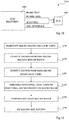
- Figure 11 is a flow diagram illustrating an example of operations in a method of fabricating a 3D circuit according to an example embodiment of the present disclosure.
- a macro wafer comprising macro circuits, and a plurality of logic chips, are fabricated.
- fabricating the macro wafer involves forming one or more macro circuits on the wafer, each macro circuit comprising a plurality of macro cells arranged in an array, the macro cells being separated from each other by spaces; and forming interconnection vias in the spaces between the macro cells.
- fabricating the macro wafer may involve forming one or more test pads on a surface of each macro circuit.
- known good dies are identified among the macro circuits on the wafer. For example, this may involve testing each macro circuit via the one or more test pads using test equipment to identify functional macro circuits. As described above with reference to Figure 5 , testing is for example performed using test pads in the metal layer before the last steps of the process that defines the bonding pads and the final planarization. This has the advantage of avoiding, in the final chip, surface degradation resulting from the testing process.
- the wafer level testing could be performed in a clean room at the fabrication site or foundry. Alternatively, the wafer could be shipped to another site for testing, and then returned to the fabrication site or foundry so that the bonding layer can be added and the final planarization performed.
- known good dies are identified among the logic chips. This may involve performing wafer level tests in a similar manner to those performed on the macro wafer, for example using test structures formed in areas of the logic wafer that will be removed during dicing. Additionally or alternatively, this may involve testing the diced logic chips.
- the thermal dissipation layer 122 is for example added before or after dicing of the logic chips.
- functional logic chips are assembled on functional macro circuits (known good dies) on the macro wafer. This for example involves selecting one or more macro circuits to form a tier of a 3D circuit from among the functional macro circuits. For example, the functional logic chips are cleaned and placed in a holder or cassette. These functional logic chips are then positioned face-to-face on the functional macro circuits of the macro wafer, and bonded at low temperature using low temperature annealing, for example at less than 500°C.
- the bonding process is a two-step process involving bonding at ambient temperature, and then annealing at around 400°C.
- thermo-compression may be employed, involving applying pressure to the top chip during at least some of the bonding process.
- dicing of the macro wafer is for example performed in order to separate the 3D circuits.
- the macro circuits Prior to dicing, the macro circuits are for example thinned to reveal the TSVs, and the micro bumps 112 of Figure 1 are added.
- each 3D circuit is then for example packaged, and further testing may be performed, for example of the 3D interfaces.
- An advantage of the method described above is that testing of both the macro chips and logic chips is possible prior to assembly, and thus 3D circuits can be assembled using only known good dies. This leads to a cost reduction with respect to a 2D circuit of corresponding area.
Landscapes
- Semiconductor Integrated Circuits (AREA)
- Design And Manufacture Of Integrated Circuits (AREA)
- Engineering & Computer Science (AREA)
- Manufacturing & Machinery (AREA)
Abstract
Description
- The present disclosure relates to the field of integrated circuits, and in particular to an integrated circuit comprising macros and logic cells and to a method of fabricating the same.
- The fabrication process of integrated circuits involves various testing operations designed to identify and discard any defective chips. For example, a typical fabrication process for integrated circuits may result in a defect rate of around 0.1 defects per in2 of silicon (equal to around 0.1 defects per 645 mm2 of silicon).
- The larger the surface area of an integrated circuit chip, the greater the risk of a defect being identified. A relatively low defect rate can therefore still lead to a high rate of discarded chips when the chip area is large. While it may be possible to repair certain types of defects, such interventions are generally time consuming and costly.
- There is thus a need in the art for an integrated circuit, and a method of fabricating the same, that leads to a reduction in the discard rate, thereby providing a corresponding cost reduction with respect to current techniques.
- It is an aim of embodiments of the present description to at least partially address one or more needs in the prior art.
- According to one aspect, there is provided a tier of a 3D circuit comprising: a stack formed of a semiconductor substrate, a transistor layer comprising transistors formed in and on the substrate, and a metal layer comprising metal levels insulated by a dielectric material, wherein one or more macro circuits are implemented in the stack, each macro circuit comprising a plurality of macro cells arranged in an array, the macro cells (202) being separated from each other by spaces; and interconnection vias positioned in the spaces between the macro cells, the interconnection vias extending through the substrate, through the transistor layer, and at least partially through the metal layer.
- According to one embodiment, one or more of the interconnection vias extend through the metal layer to a corresponding interconnection pad formed on the surface of the metal layer for interconnecting with a second tier.
- According to one embodiment, the interconnection vias are positioned at regular intervals.
- According to one embodiment, the tier further comprises micro bumps positioned on one side of the substrate, each of the interconnection vias being connected to a corresponding one of the micro bumps.
- According to one aspect, there is provided a tier of a 3D circuit comprising: one or more macro circuits, each macro circuit comprising a plurality of macro cells arranged in an array, the macro cells being separated from each other by spaces; and interconnection vias positioned in the spaces between the macro cells.
- According to one embodiment, the tier comprises a stack formed of a substrate, a transistor layer and a metal layer, the interconnection vias extending at least partially through the substrate, through the transistor layer and to the metal layer.
- According to one embodiment, the tier further comprises interconnection pads formed on the surface of the metal layer.
- According to a further aspect, there is provided a 3D circuit comprising: a first tier comprising the above tier; and a second tier stacked on the first tier and comprising a logic circuit connected via interconnection pads to the one or more macro circuits of the first tier.
- According to one embodiment, at least a first one of the interconnection vias is coupled to a supply voltage rail of the first tier for supplying a supply voltage to the first tier, and/or at least a second one of the interconnection vias is coupled to a supply voltage rail of the second tier for supplying a supply voltage to the second tier.
- According to one embodiment, the 3D circuit further comprises micro bumps positioned on one side of the substrate and connected to the interconnection vias.
- According to one embodiment, the logic circuit is connected to the interconnection vias of the first tier via metal connections formed in a metal layer of the first tier.
- According to one embodiment, the first tier comprises transistors fabricated using a first transistor technology, and the second tier comprises transistors fabricated using a second transistor technology different to the first transistor technology.
- According to a further aspect, there is provided a wafer comprising: a plurality of the above tiers arranged in columns and rows and separated by dicing lines.
- According to one embodiment, each macro circuit comprises one or more test pads permitting the macro circuit to be tested.
- According to a further aspect, there is provided a test system for testing the macro circuits of the above wafer, the test system comprising test equipment coupled to the one or more test pads via one or more test probes.
- According to a further aspect, there is provided a method of fabricating a tier of a 3D circuit, the method comprising: forming one or more macro circuits, each macro circuit comprising a plurality of macro cells arranged in an array, the macro cells being separated from each other by spaces, the macro circuits being formed in a stack formed of a semiconductor substrate, a transistor layer comprising transistors formed in and on the substrate, and a metal layer comprising metal levels insulated by a dielectric material; and forming interconnection vias in the spaces between the macro cells, the interconnection vias extending through the substrate, through the transistor layer, and at least partially through the metal layer.
- According to yet a further aspect, there is provided a method of fabricating a tier of a 3D circuit, the method comprising: forming one or more macro circuits, each macro circuit comprising a plurality of macro cells arranged in an array, the macro cells being separated from each other by spaces; and forming interconnection vias in the spaces between the macro cells.
- According to one embodiment, forming the one or more macro circuits comprises forming a stack comprising a substrate, a transistor layer and a metal layer, the interconnection vias being formed such that they extend at least partially through the substrate, through the transistor layer and to the metal layer.
- According to one embodiment, the method further comprises: forming one or more test pads on a surface of each macro circuit; and testing, using test equipment, each macro circuit via the one or more test pads to identify functional macro circuits.
- According to one embodiment, the one or more macro circuits are formed on a wafer along with further macro circuits, the method further comprising: selecting the one or more macro circuits to form the tier of the 3D circuit from among the functional macro circuits; and performing dicing to separate the one or more macro circuits from the wafer.
- According to a further aspect, there is provided a method of fabricating a 3D circuit, the method comprising:
- fabricating a first tier according to the above method;
- fabricating a second tier comprising a logic circuit; and stacking the second tier on the first tier.
- The foregoing and other features and advantages will become apparent from the following detailed description of embodiments, given by way of illustration and not limitation with reference to the accompanying drawings, in which:
-
Figure 1 is a cross-section view of a 3D circuit according to an example embodiment of the present disclosure; -
Figure 2 is a plan view of a macro tier of the 3D circuit ofFigure 1 according to an example embodiment of the present disclosure; -
Figure 3 is a plan view of several macro cells of the macro tier ofFigure 2 according to an example embodiment of the present disclosure; -
Figure 4 shows cross-section views of a portion of a macro wafer during its fabrications according to an example embodiment of the present disclosure; -
Figure 5 shows cross-section views of a logic wafer during the fabrication of logic chips according to an example embodiment of the present disclosure; -
Figure 6 is a cross-section view of an assembly operation of the logic chips ofFigure 5 on the wafer ofFigure 4 according to an example embodiment of the present disclosure; -
Figure 7 is a cross-section view of 3D circuits resulting from the operations ofFigure 4 to 6 ; -
Figure 8 is a plan view of a macro circuit according to an example embodiment of the present disclosure; -
Figure 9 is a plan view of a macro wafer prior to and following dicing; -
Figure 10 schematically illustrates a test system according to an example embodiment of the present disclosure; and -
Figure 11 is a flow diagram representing operations in a method of fabricating a 3D circuit according to an example embodiment of the present disclosure. - It should be noted that the various views of integrated circuits in the various figures are not drawn to scale.
- In following description, unless specified otherwise, the expressions "around", "approximately", "substantially" and "in the order of" signify within 10 %, and preferably within 5 %.
-
Figure 1 illustrates a3D circuit 100 according to an example embodiment of the present disclosure. The3D circuit 100 comprises two tiers T1 and T2 respectively corresponding tointegrated circuit chips - More generally, a 3D circuit is considered herein to be a circuit having any plurality of tiers stacked one upon the other, each tier having a transistor layer, in other words an active layer in which transistor devices are formed, and an interconnection layer in which interconnections between the transistor devices, and from the transistor devices to one or more other tiers, are formed.
- The present inventors have noticed that in digital circuits or mixed digital/analog circuits, the surface area occupied by logic cells, i.e. standard cells, tends to correspond to up to 50 percent of the total surface area. The rest is occupied by larger macros, sometime referred to as IP (intellectual property) circuits. The
3D circuit 100 ofFigure 1 exploits this trend. In particular, thechip 101 for example corresponds to a macro tier, in which one or more macro circuits are implemented, while the chip of tier T2 for example corresponds to a logic tier, in which logic cells, or standard cells, are implemented. In some embodiments, the macro circuits and logic circuits of the circuit design may have non-equal surface requirements. In such a case, the tier T2 may additionally comprise one or more macros, and/or one or more of the macro circuits may be dummy circuits that are non-active and not used during the lifetime of the 3D circuit. - As known by those skilled in the art, logic cells are relatively small circuits comprising digital logic devices that are used to implement Boolean logic functions, such as AND, OR, NOR, XOR and XNOR gates, or basic storage functions, such as latches and flip-flips. These logic cells are generated by the circuit conception tool during a synthesis operation based on code defining the functionality of the logic cells, for example in the form of RTL (Register Transfer Level) code. Each logic cell is for example selected from a library of standard cells of the targeted technology.
- As also known in the art, macros are generally larger circuits that may comprise logic cells and other circuitry including analog circuits. The design of a macro, including the positioning within the macro of the various cells of the macro and the interconnections between these cells, can be considered to be fixed, in other words it is not modified during the circuit synthesis and place and route operations.
- In some embodiments, the same transistor technology can be used to fabricate the
circuits circuits circuits logic circuit 102 could be fabricated using 28 nm FinFET technology, and themacro circuit 101 could be fabricated using 10 nm finFET technology in the case that the macros are SRAM memories, or the technology known in the art as relaxed node 65 nm technology in the case that the macros comprise analog devices. - The
chip 101 for example comprises asubstrate 104, for example formed of silicon or another semiconductor, atransistor layer 106 formed on thesubstrate 104 and for example comprising transistor gate stacks formed on thesubstrate 104, and ametal layer 108 formed on the transistor layer and comprising levels of metal interconnecting transistors of thetransistor layer 106. For example, the metal layer comprises a layer of dielectric material in which levels of metal in defined patterns have been formed in order to provide connections between the transistors or other devices formed in the transistor layer. - A number of interconnection vias, such as TSVs (through silicon vias), 110 extend from the
metal layer 108, through thetransistor layer 106 andsubstrate 104, to an underside or backside of thechip 101, where they are for example connected tomicro bumps 112. - The
chip 102 for example comprises asubstrate 114, for example formed of silicon or another semiconductor, atransistor layer 116 formed on thesubstrate 114 and for example comprising transistor gate stacks formed on thesubstrate 114, and ametal layer 118 formed on the transistor layer and comprising levels of metal interconnecting transistors of thetransistor layer 116. -
Interconnections 120, for example comprising copper-to-copper bonding pads, are formed between the metal layers 108 and 118 of thechips heat spreader 122 is for example formed on the backside of thechip 102. Thechip 101 is for example mounted on apackage substrate 124 via the micro bumps 112. Thepackage substrate 124 for example comprises connecting vias (not represented inFigure 1 ) between themicro bumps 112 and BGA (Ball Grid Array) balls 126 positioned on an underside of thepackage substrate 124. The BGA balls 126 are for example used for electrically connecting the package to a circuit board (not illustrated) . - An interface between the logic circuit of the
chip 102 and the one or more macro circuits of thechip 101 is for example implemented by an RDL (redistribution layer), for example a hybrid bonding layer between the chips. For example, this layer comprises interconnection pads having a pitch of between 1 and 10 µm. - While in the example of
Figure 1 theinterconnection vias 110 each extend to one or more metal levels in themetal layer 108, in some embodiments, one or more of theinterconnection vias 110 extend to acorresponding interconnection pad 120 formed on the surface of themetal layer 108 for interconnecting with the tier T2. - The interconnection vias 110 are for example formed at regular intervals in spaces formed between macro circuits formed in the tier T1. In some embodiments, one or more of the interconnection vias is coupled to a supply voltage rail of the first tier for supplying a supply voltage, such as a VDD or GND voltage, to the first tier, and/or one or more of the interconnection vias is coupled to a supply voltage rail of the second tier for supplying a supply voltage, such as a VDD or GND voltage, to the second tier. An advantage of providing supply voltages to the tier T1 and/or tier T2 via regularly spaced interconnection vias is that they can be used to supply the voltage supply rails of the tiers, which are for example regularly spaced in the metal layers 108, 118 of the respective tiers. Advantageously, this permits either or both tiers to be supplied with relatively low IR (current resistance) drop.
- Furthermore, while in the embodiment of
Figure 1 the tiers T1 and T2 are stacked face-to-face, in alternative embodiments, they could be stacked back-to-face, for example with thesubstrate 114 of the tier T2 contacting themetal layer 108 of the tier T1. In such a case, the tier T2 for example comprises interconnection vias extending from theinterconnection pads 120, through thesubstrate 114 andtransistor layer 116, to themetal layer 118 of the tier T2. - An advantage of the
circuit 100 ofFigure 1 is that, by implementing a circuit using two separate chips, the surface area of each chip is considerably reduced, thereby reducing the probability of a defect being present on either chip following fabrication. By identifying and selecting only known good dies (KGDs) to be assembled to form the 3D circuit, the overall discard rate of the chips can be reduced, leading to a cost reduction. - Furthermore, the logic circuit of the
chip 102 can be designed without the need of 3D interconnections traversing this layer. Thus the design overhead due to the 3D technology is relatively little as concerns the logic circuit. By placing the macros of the circuit in thechip 101, which is traversed by TSVs, a relatively simple design can be adopted that has an efficient use of surface area, as will now be described in more detail with reference toFigures 2 and 3 . -
Figure 2 is a plan view of thechip 101 according to an example embodiment. As illustrated, thechip 101 for example comprises an array ofmacro cells 202. As will be described in more detail below with reference toFigures 8 and 9 , in some embodiments these macro cells form one or more macro circuits. - Each
macro cell 202 for example implements a memory array, such as an SRAM (Static Random Access Memory) array, although other types of macro cells could also be implemented, including other types of memories or register banks, data processors, or even analog circuits that can be implemented in a modular fashion. In the example ofFigure 2 , each of themacro cells 202 has the same size, but in alternative embodiments, it would be possible to implement macro cells of different sizes. - The
TSVs 110 are located in gaps between themacro cells 202, and for example at regular intervals. For example, the macro cells are square or rectangular in shape, and theTSVs 110 traverse the chip in the space separating adjacent corners of themacro cells 202. Other positions of the TSVs around themacro cells 202 would also be possible. -
Figure 2 also represents, using dashed squares, theinterconnection pads 120 formed on top of the metal layers of thechip 101. For example, thesepads 120 are formed in a hybrid bonding (HB) layer. Thesepads 120 are for example formed in an array having a regular pitch, the pitch for example being in the range 1 to 10 µm as mentioned above. For ease of illustration, thepads 120 inFigure 2 are illustrated having a relatively high pitch. - An advantage of separating the logic cells of the design from the macro cells is that this facilitates the physical implementation of the design, including the floor planning, by removing physical constraints encountered when connections between logic cells must pass around intermediate macro cells. By forming the logic cells and macro cells on different layers, the connections between the logic cells, and between the logic cells and macro cells, can be short and thus provide rapid and efficient electrical connections.
- A circuit conception method for generating a 3D circuit layout that could be used for designing the
chip 102 is described in the patent application entitled "Conception of a 3D circuit comprising macros" having the same filing date and applicant as the present case (law firm reference B16909, applicant reference DD18558ST), the contents of which is hereby incorporated by reference. Indeed, that patent application describes generating a 3D circuit in which one tier comprises only macros and the other tier comprises a logic circuit, and optionally one or more macros. For example, the physical implementation of the 3D circuit ofFigure 1 , involving synthesis and place and route, is based on timing and power files (for example .lib files) and physical abstract view files (for example .lef files) defining the macro circuits of the design. In some embodiments, a timing and power file (.lib file) is provided having added routing nets for reaching 3D contacts of the macro circuits, and a physical abstract view file (.lef file) is provided in which each macro circuit is encapsulated into the metal layer of the structure, and the position of the pins is defined. A designer can than base the physical implementation of the logic circuits on a model defined by these files and defining in particular the floorplan and pin positions of each macro circuit. -
Figure 3 is a plan view showing four of themacro cells 202 ofFigure 2 in more detail. As illustrated, eachTSV 110 is for example surrounded by anexclusion zone 302, which is for example circular, and represents a zone that cannot be covered by themacro cells 202. EachTSV 110 for example has a diameter d1 of between 3 and 10 µm, and for example of around 5 µm. Theexclusion zones 302 for example have diameters d2 of between 5 and 20 µm, and for example of around 10 µm. In some embodiments, amacro cell 202 cannot cover a region within around 5 µm of a TSV. The pitch p of the TSVs, in other words the separation between adjacent TSVs, is for example between 50 and 500 µm, depending on the sizes of the macro cells, and may be different in the horizontal and vertical directions. The gap g between adjacent macro cells is for example equal to around the width of the keep outzones 302, and is for example around 15 µm. In one embodiment, thechip 101 has a surface area of between 100 mm2 and 200 mm2, and a width w and height h of between around 10 mm and 15 mm. The pitch p is for example equal to between 100 and 300 µm, and for example around 150 µm. - In some embodiments, one or
more test circuits 204, which are for example built-in self-test (BIST) circuits, are formed in thechip 102 and associated with eachmacro cell 202. Alternatively, each BIST circuit could be shared by more than onemacro cell 202. These BIST circuits permit the macro cells to be tested. For example, theBIST circuits 204 have access to one or more input pins 206 and one ormore output pins 208 of eachmacro cell 202. In the case that themacro cells 202 implement memory circuits, the input pins 206 for example include clock, address and data pins, and the output pins 208 for example include data pins. For ease of illustration, examples of input andoutput pins Figure 3 in relation with only one of the macro cells. -
Figure 4 shows cross-section views of a portion of a macro wafer during fabrication of macro chips or tiers of a 3D circuit according to an example embodiment of the present disclosure. - As represented in a first view (a) of
Figure 4 , the macro wafer is for example fabricated using asilicon substrate 402 on which atransistor layer 404 is formed, and theTSVs 110 are also formed down from the surface of thetransistor layer 404 but only partially traversing thesilicon substrate 402. The example ofFigure 4 represents the formation of three adjacent macro chips ortiers - As represented in a second view (b) of
Figure 4 , ametal layer 412 is then for example formed over the wafer, comprising metal levels connecting with nodes of the transistors in thetransistor layer 404, and with theTSVs 110. In some embodiments,test pads 414 are formed at this stage, exposed on the surface of themetal layer 412. These test pads are for example connected to at least some of the transistors of the devices, and permit a wafer level testing of the macro circuits. - As represented in a third view (c) of
Figure 4 , a copper bonding layer is then for example added to themetal layer 412, this copper bonding layer comprisinginterconnection pads 416, for example formed of copper, and exposed on the surface of themetal layer 412 to permit electrical bonding with the logic circuits. In some embodiments, prior to forming the copper bonding layer, thetest pads 414 are removed, for example using a CMP (chemical-mechanical polishing) step. -
Figure 5 shows cross-section views of a portion of a logic wafer during the fabrication of logic chips according to an example embodiment of the present disclosure. - As represented in a first view (a) of
Figure 5 , the logic wafer is for example fabricated using asilicon substrate 502 on which atransistor layer 504 is formed, and ametal layer 506 is formed over thetransistor layer 504. Themetal layer 506 for example comprisesinterconnection pads 508, for example formed of copper, that provide a copper bonding layer for connection with theinterconnection pads 416 of the macros. The example ofFigure 5 represents the formation of fouradjacent logic chips Figure 5 , during the formation of themetal layer 506, test pads could be formed and removed permitting the testing of the logic circuits in a similar manner to thetest pads 414 of the macro wafer described above. - As represented in a second view (b) of
Figure 5 , thesilicon substrate 502 is for example thinned, leaving a relatively thin layer 502' of silicon of for example around 200 µm in thickness, and ahandle wafer 518 may be added. Alternatively, the thinning could be performed after assembly. - As represented in a third view (c)
Figure 5 , dicing is then for example performed to separate the wafer into theindividual chips layers substrate 114,transistor layer 116 andmetal layer 118 of the logic chips. Thehandle wafer 518 for example becomes a handle layer 518' on each chip. -
Figure 6 is a cross-section view of the assembly of logic circuits ofFigure 5 with the wafer ofFigure 4 . - Functional logic chips (i.e. known good dies) are for example bonded to functional macro circuits (i.e. known good dies) on the macro wafer. In the example of
Figure 6 , thelogic chips macro chips chips macro chips logic chips - In the example of
Figure 6 , themacro chip 410 has been found to have one or more defects, and therefore no logic circuit is assembled on this macro chip. -
Figure 7 represents 3D circuits after thinning of thesubstrate 402 to expose theTSVs 110, removal of the handle layers 518', the addition ofmicro bumps 112 and dicing of the macro wafer ofFigure 6 . Furthermore, the 3D circuit has been mounted on theBGA grid package 124. -
Figure 8 is a plan view of amacro circuit 800 according to an example embodiment. Themacro circuit 800 for example comprises an array ofmacro cells 202, and asealring 802 surrounding the array of macro cells. The sealring for example prevents delamination of the chip during dicing. In the example ofFigure 8 , the array of macro cells is a 60 by 60 array, although other dimensions would be possible. - The
macro circuit 800 for example has dimensions of around 1 cm by 1 cm, and thus a surface area of around 1 cm2, although other dimensions would be possible. More generally, the surface area or eachmacro circuit 800 is for example of between 0.2 cm2 and 8 cm2, or up to the size of the reticle used for fabrication. In the case that themacro circuit 800 corresponds to a memory array, such as an SRAM, eachmacro cell 202 for example has a storage capacity of around 100 Kbits, and thus the 60 by 60 array for example has a storage capacity of around 360 Mbits. - As mentioned above in relation with
Figure 2 , thechip 101 of the3D circuit 100 ofFigure 1 may comprise one or more macro circuits, as will now be described in more detail with reference toFigure 9 . -
Figure 9 illustrates aportion 900 of a wafer on whichmacro circuits 800 are formed in columns and rows. Each column ofmacro circuits 800 is for example separated by a spacing scl large enough for a cut to be performed.Vertical cut lines 902 are represented by vertical dashed lines between the columns of macro circuits inFigure 9 . Similarly, each row ofmacro circuits 800 is for example separated by a spacing scl' large enough for a cut to be performed.Horizontal cut lines 904 are represented by horizontal dashed lines between the rows of macro circuits inFigure 9 . - During a dicing operation, the wafer of
Figure 9 is for example cut to form the macro chips or tiers each comprising one, two, three, four or moremacro circuits 800, depending on the application.Figure 9 illustrates an example of twochips 101 each comprising a singlemacro circuit 800, and of achip 101 comprising fourmacro circuits 800, although other sizes would be possible. - In some embodiments, the area of the chip containing the macro circuit or circuits is greater than or equal to the area of the logic circuit to be stacked on the macro chip, and the logic chip does not having any overhanging portions.
- It will be noted that, in the case that the
chip 101 comprises more than onemacro circuit 800, there is an interruption in the regular spacing of themacro cells 202 at the border between adjacentmacro circuits 800. In some embodiments, thecells 202, the spacing scl, and theTSVs 110 are arranged such that the distance d4 betweenadjacent TSVs 110 of adjacent macro circuits is equal to the pitch p (seeFigure 3 ) of the TSVs within eachmacro circuit 800. In other words, the width of two adjacent seal rings 802 and the spacing scl between the sealrings is substantially equal to the width of amacro cell 202. For example, each sealring has a width of around 30 µm and the spacing scl of the dicing line is chosen to equal 90 µm, leading to a total distance of 150 µm (30+90+30), which corresponds to a pitch of the TSVs of 150 µm. - In the case that the TSV pitch within each
macro circuit 800 is relatively small, for example less than 100 µm, the distance d4 betweenadjacent TSVs 110 of adjacent macro circuits could be a multiple of this pitch, for example two or three times the pitch. This implies that there would simply be one or more missing columns or rows of TSVs between adjacent macro circuits in the otherwise regular TSV matrix. - It is considered in the above that the designer of the macro circuits is capable of applying a regular pitch to the TSVs within each macro circuit. For example, the 10 (Input/Output) pads of the macro circuits, which for example comprise buffers and/or ESD (Electro-Static Discharge) protection, are for example positioned around the macro cells or between the macro cuts, such that a regular TSV pitch can be maintained.
- Alternatively, there may be a discontinuity in the pitch between the TSVs at the border between adjacent
macro circuits 800, and/or within each macro circuit. - In any case, files defining the layout of the
macro chip 101 and of the macro cells on this chip for example indicate to a designer of the logic circuit the positions of the TSVs having a regular or irregular pitch. -
Figure 10 schematically illustrates atesting system 1000 for testing a device-under-test (DUT) 1002, which is for example themacro circuit 800 or logic circuit described herein. The testing is for example at least partially performed on the individual dies at the wafer level before dicing, such that EWS (Electrical Wafer Sorting) may be performed and only known good dies are subsequently assembled. - The
system 1000 for example comprises test equipment (TEST EQUIPMENT) 1004 capable of testing theDUT 1002 over a number of different test interfaces. For example, the test equipment may include a probe test (PROBE TEST), involving the use of one or more probes to make electrical contact with one or more test pads formed on a surface of the circuits to be tested, as described above. During this test, the test equipment may additionally have access to the power grids (POWER GRID) of the circuit, such that the individual dies on the circuit can be powered during the test. The test equipment may also be capable of performing a scan test (SCAN TEST) of theDUT 1004 via a test access mechanism (TAM) using a TAM protocol such as the JTAG standard IEEE 1500. A BIST circuit may also be present in the macro circuits and/or logic circuits, and the test equipment may be capable of accessing this BIST circuit via an appropriate interface. -
Figure 11 is a flow diagram illustrating an example of operations in a method of fabricating a 3D circuit according to an example embodiment of the present disclosure. - In an
operation 1101, a macro wafer comprising macro circuits, and a plurality of logic chips, are fabricated. For example, as described above, fabricating the macro wafer involves forming one or more macro circuits on the wafer, each macro circuit comprising a plurality of macro cells arranged in an array, the macro cells being separated from each other by spaces; and forming interconnection vias in the spaces between the macro cells. Furthermore, fabricating the macro wafer may involve forming one or more test pads on a surface of each macro circuit. - In an
operation 1102, known good dies are identified among the macro circuits on the wafer. For example, this may involve testing each macro circuit via the one or more test pads using test equipment to identify functional macro circuits. As described above with reference toFigure 5 , testing is for example performed using test pads in the metal layer before the last steps of the process that defines the bonding pads and the final planarization. This has the advantage of avoiding, in the final chip, surface degradation resulting from the testing process. The wafer level testing could be performed in a clean room at the fabrication site or foundry. Alternatively, the wafer could be shipped to another site for testing, and then returned to the fabrication site or foundry so that the bonding layer can be added and the final planarization performed. - In an
operation 1103, known good dies are identified among the logic chips. This may involve performing wafer level tests in a similar manner to those performed on the macro wafer, for example using test structures formed in areas of the logic wafer that will be removed during dicing. Additionally or alternatively, this may involve testing the diced logic chips. Thethermal dissipation layer 122 is for example added before or after dicing of the logic chips. - In an
operation 1104, functional logic chips (known good dies) are assembled on functional macro circuits (known good dies) on the macro wafer. This for example involves selecting one or more macro circuits to form a tier of a 3D circuit from among the functional macro circuits. For example, the functional logic chips are cleaned and placed in a holder or cassette. These functional logic chips are then positioned face-to-face on the functional macro circuits of the macro wafer, and bonded at low temperature using low temperature annealing, for example at less than 500°C. In some embodiments, the bonding process is a two-step process involving bonding at ambient temperature, and then annealing at around 400°C. Furthermore, thermo-compression may be employed, involving applying pressure to the top chip during at least some of the bonding process. - In an
operation 1105, dicing of the macro wafer is for example performed in order to separate the 3D circuits. Prior to dicing, the macro circuits are for example thinned to reveal the TSVs, and themicro bumps 112 ofFigure 1 are added. - In an
operation 1106, each 3D circuit is then for example packaged, and further testing may be performed, for example of the 3D interfaces. - An advantage of the method described above is that testing of both the macro chips and logic chips is possible prior to assembly, and thus 3D circuits can be assembled using only known good dies. This leads to a cost reduction with respect to a 2D circuit of corresponding area.
- Having thus described at least one illustrative embodiment, various alterations, modifications and improvements will readily occur to those skilled in the art. For example, it will be apparent to those skilled in the art that while examples have been provided in which the macro circuits correspond to memory arrays, other types of circuits would be possible, including analog circuits. Furthermore, it will be apparent to those skilled in the art that the
logic chip 102 described herein could include one or more macros. - Furthermore, it will be apparent to those skilled in the art that the various features described in relation with the various embodiments could be combined, in alternative embodiments, in any combination.
Claims (15)
- A tier of a 3D circuit comprising:a stack formed of a semiconductor substrate (104), a transistor layer (106) comprising transistors formed in and on the substrate, and a metal layer (108) comprising metal levels insulated by a dielectric material, wherein one or more macro circuits (800) are implemented in the stack, each macro circuit comprising a plurality of macro cells (202) arranged in an array (101), the macro cells (202) being separated from each other by spaces; andinterconnection vias (110) positioned in the spaces between the macro cells (202), the interconnection vias (110) extending through the substrate (104), through the transistor layer (106), and at least partially through the metal layer (108) .
- The tier of claim 1, wherein one or more of the interconnection vias (110) extend through the metal layer (108) to a corresponding interconnection pad (416) formed on the surface of the metal layer (108) for interconnecting with a second tier (T2) .
- The tier of claim 1 or 2, wherein the interconnection vias (110) are positioned at regular intervals.
- The tier of any of claims 1 to 3, further comprising micro bumps (112) positioned on one side of the substrate, each of the interconnection vias (110) being connected to a corresponding one of the micro bumps.
- A 3D circuit comprising:a first tier (T1) comprising the tier of any of claims 1 to 4; anda second tier (T2) stacked on the first tier and comprising a logic circuit (102) connected via interconnection pads (416) to the one or more macro circuits of the first tier (T1) .
- The 3D circuit of claim 5, wherein at least a first one of the interconnection vias (110) is coupled to a supply voltage rail (VDD, GND) of the first tier (T1) for supplying a supply voltage to the first tier, and/or at least a second one of the interconnection vias (110) is coupled to a supply voltage rail (VDD, GND) of the second tier (T2) for supplying a supply voltage to the second tier.
- The 3D circuit of claim 5 or 6, wherein the logic circuit (102) is connected to the interconnection vias (110) of the first tier (T1) via metal connections formed in a metal layer (108) of the first tier (T1).
- The 3D circuit of any of claims 5 to 7, wherein the first tier (T1) comprises transistors fabricated using a first transistor technology, and the second tier (T2) comprises transistors fabricated using a second transistor technology different to the first transistor technology.
- A wafer comprising:
a plurality of the tiers (800) of any of claims 1 to 3 arranged in columns and rows and separated by dicing lines. - The wafer of claim 9, wherein each macro circuit comprises one or more test pads (414) permitting the macro circuit to be tested.
- A test system for testing the macro circuits of a wafer according to claim 9, the test system comprising test equipment (1004) coupled to the one or more test pads (414) via one or more test probes.
- A method of fabricating a tier of a 3D circuit, the method comprising:forming one or more macro circuits (800), each macro circuit comprising a plurality of macro cells (202) arranged in an array (101), the macro cells (202) being separated from each other by spaces, the macro circuits being formed in a stack formed of a semiconductor substrate (104), a transistor layer (106) comprising transistors formed in and on the substrate, and a metal layer (108) comprising metal levels insulated by a dielectric material; andforming interconnection vias (110) in the spaces between the macro cells (202), the interconnection vias (110) extending through the substrate (104), through the transistor layer (106), and at least partially through the metal layer (108).
- The method of claim 12, further comprising:forming one or more test pads (414) on a surface of each macro circuit; andtesting, using test equipment (1004), each macro circuit via the one or more test pads to identify functional macro circuits.
- The method of claim 12 or 13, wherein the one or more macro circuits (800) are formed on a wafer along with further macro circuits, the method further comprising:selecting the one or more macro circuits to form the tier of the 3D circuit from among the functional macro circuits; andperforming dicing to separate the one or more macro circuits from the wafer.
- A method of fabricating a 3D circuit, the method comprising:fabricating a first tier (T1) according to the method of any of claims 12 to 14;fabricating a second tier (T2) comprising a logic circuit; andstacking the second tier (T2) on the first tier (T1).
Applications Claiming Priority (1)
| Application Number | Priority Date | Filing Date | Title |
|---|---|---|---|
| FR1855325A FR3082656B1 (en) | 2018-06-18 | 2018-06-18 | INTEGRATED CIRCUIT COMPRISING MACROS AND ITS MANUFACTURING METHOD |
Publications (1)
| Publication Number | Publication Date |
|---|---|
| EP3584825A1 true EP3584825A1 (en) | 2019-12-25 |
Family
ID=63684025
Family Applications (1)
| Application Number | Title | Priority Date | Filing Date |
|---|---|---|---|
| EP19180679.3A Pending EP3584825A1 (en) | 2018-06-18 | 2019-06-17 | Integrated circuit comprising macros and method of fabricating the same |
Country Status (3)
| Country | Link |
|---|---|
| US (1) | US10937778B2 (en) |
| EP (1) | EP3584825A1 (en) |
| FR (1) | FR3082656B1 (en) |
Families Citing this family (8)
| Publication number | Priority date | Publication date | Assignee | Title |
|---|---|---|---|---|
| US11569219B2 (en) * | 2020-10-22 | 2023-01-31 | Arm Limited | TSV coupled integrated circuits and methods |
| KR20220065292A (en) * | 2020-11-13 | 2022-05-20 | 삼성전자주식회사 | Semiconductor package and method of manufacturing the same |
| US11894356B2 (en) * | 2021-08-17 | 2024-02-06 | Macronix International Co., Ltd. | Chip having multiple functional units and semiconductor structure using the same |
| CN116092960A (en) * | 2021-11-05 | 2023-05-09 | 安徽寒武纪信息科技有限公司 | Wafer testing method, storage medium, computer program product and device |
| CN118872067A (en) | 2021-12-20 | 2024-10-29 | 蒙德无线公司 | Semiconductor devices for RF integrated circuits |
| TWI790139B (en) * | 2022-03-09 | 2023-01-11 | 力晶積成電子製造股份有限公司 | Through-substrate via test structure |
| CN117320433A (en) * | 2022-06-28 | 2023-12-29 | 联咏科技股份有限公司 | Semiconductor device |
| US20240213217A1 (en) * | 2022-12-21 | 2024-06-27 | International Business Machines Corporation | Clustering fine pitch micro-bumps for packaging and test |
Citations (9)
| Publication number | Priority date | Publication date | Assignee | Title |
|---|---|---|---|---|
| US4799009A (en) * | 1979-10-25 | 1989-01-17 | Vlsi Technology Research Association | Semiconductor testing device |
| US20010033030A1 (en) * | 1997-04-04 | 2001-10-25 | Elm Technology Corporation | Three dimensional structure integrated circuits |
| US6376909B1 (en) * | 1999-09-02 | 2002-04-23 | Micron Technology, Inc. | Mixed-mode stacked integrated circuit with power supply circuit part of the stack |
| US20080273361A1 (en) * | 2007-05-02 | 2008-11-06 | Dudeck Dennis E | Memory Cell for Content-Addressable Memory |
| US20090111215A1 (en) * | 2007-10-30 | 2009-04-30 | International Business Machines Corporation | Modular Chip Integration Techniques |
| US8629548B1 (en) * | 2012-10-11 | 2014-01-14 | Easic Corporation | Clock network fishbone architecture for a structured ASIC manufactured on a 28 NM CMOS process lithographic node |
| US20140377886A1 (en) * | 2013-06-25 | 2014-12-25 | Micron Technology, Inc. | Method of manufacturing semiconductor device including grinding semiconductor wafer |
| US20160042110A1 (en) * | 2014-08-10 | 2016-02-11 | Qualcomm Incorporated | High quality physical design for monolithic three-dimensional integrated circuits (3d ic) using two-dimensional integrated circuit (2d ic) design tools |
| US20160190101A1 (en) * | 2014-02-20 | 2016-06-30 | Taiwan Semiconductor Manufacturing Company, Ltd. | Functional block stacked 3dic and method of making same |
Family Cites Families (22)
| Publication number | Priority date | Publication date | Assignee | Title |
|---|---|---|---|---|
| US6271542B1 (en) | 1997-12-08 | 2001-08-07 | International Business Machines Corporation | Merged logic and memory combining thin film and bulk Si transistors |
| JP3532788B2 (en) | 1999-04-13 | 2004-05-31 | 唯知 須賀 | Semiconductor device and manufacturing method thereof |
| JP2003185710A (en) | 2001-10-03 | 2003-07-03 | Matsushita Electric Ind Co Ltd | Multi-chip module, semiconductor chip, and inter-chip connection test method of multi-chip module |
| US20050127490A1 (en) | 2003-12-16 | 2005-06-16 | Black Bryan P. | Multi-die processor |
| JP2007265019A (en) | 2006-03-28 | 2007-10-11 | Sony Computer Entertainment Inc | Arithmetic processing unit |
| US7616470B2 (en) | 2006-06-16 | 2009-11-10 | International Business Machines Corporation | Method for achieving very high bandwidth between the levels of a cache hierarchy in 3-dimensional structures, and a 3-dimensional structure resulting therefrom |
| US8110899B2 (en) | 2006-12-20 | 2012-02-07 | Intel Corporation | Method for incorporating existing silicon die into 3D integrated stack |
| US7863733B2 (en) | 2007-07-11 | 2011-01-04 | Arm Limited | Integrated circuit with multiple layers of circuits |
| US7816934B2 (en) | 2007-10-16 | 2010-10-19 | Micron Technology, Inc. | Reconfigurable connections for stacked semiconductor devices |
| JP2009283515A (en) * | 2008-05-19 | 2009-12-03 | Panasonic Corp | Semiconductor integrated circuit |
| US20100140750A1 (en) | 2008-12-10 | 2010-06-10 | Qualcomm Incorporated | Parallel Plane Memory and Processor Coupling in a 3-D Micro-Architectural System |
| IT1398204B1 (en) * | 2010-02-16 | 2013-02-14 | St Microelectronics Srl | SYSTEM AND METHOD TO PERFORM THE ELECTRIC TEST OF THROUGH THE SILICON (TSV - THROUGH SILICON VIAS). |
| WO2011107612A1 (en) | 2010-03-05 | 2011-09-09 | Imec | Customizable interconnections between electronic circuits |
| US8549447B2 (en) * | 2010-04-24 | 2013-10-01 | Robert Eisenstadt | Integrated circuits with multiple I/O regions |
| US8648615B2 (en) | 2010-06-28 | 2014-02-11 | Xilinx, Inc. | Testing die-to-die bonding and rework |
| TW201225249A (en) * | 2010-12-08 | 2012-06-16 | Ind Tech Res Inst | Stacked structure and stacked method for three-dimensional integrated circuit |
| US9201834B2 (en) * | 2011-10-11 | 2015-12-01 | Etron Technology, Inc. | Reconfigurable high speed memory chip module and electronic device with a reconfigurable high speed memory chip module |
| US9236864B1 (en) | 2012-01-17 | 2016-01-12 | Altera Corporation | Stacked integrated circuit with redundancy in die-to-die interconnects |
| US20150279431A1 (en) | 2014-04-01 | 2015-10-01 | Micron Technology, Inc. | Stacked semiconductor die assemblies with partitioned logic and associated systems and methods |
| US9666562B2 (en) | 2015-01-15 | 2017-05-30 | Qualcomm Incorporated | 3D integrated circuit |
| US9741691B2 (en) | 2015-04-29 | 2017-08-22 | Qualcomm Incorporated | Power delivery network (PDN) design for monolithic three-dimensional (3-D) integrated circuit (IC) |
| KR102406583B1 (en) * | 2017-07-12 | 2022-06-09 | 삼성전자주식회사 | Semiconductor device |
-
2018
- 2018-06-18 FR FR1855325A patent/FR3082656B1/en active Active
-
2019
- 2019-06-17 US US16/443,441 patent/US10937778B2/en active Active
- 2019-06-17 EP EP19180679.3A patent/EP3584825A1/en active Pending
Patent Citations (9)
| Publication number | Priority date | Publication date | Assignee | Title |
|---|---|---|---|---|
| US4799009A (en) * | 1979-10-25 | 1989-01-17 | Vlsi Technology Research Association | Semiconductor testing device |
| US20010033030A1 (en) * | 1997-04-04 | 2001-10-25 | Elm Technology Corporation | Three dimensional structure integrated circuits |
| US6376909B1 (en) * | 1999-09-02 | 2002-04-23 | Micron Technology, Inc. | Mixed-mode stacked integrated circuit with power supply circuit part of the stack |
| US20080273361A1 (en) * | 2007-05-02 | 2008-11-06 | Dudeck Dennis E | Memory Cell for Content-Addressable Memory |
| US20090111215A1 (en) * | 2007-10-30 | 2009-04-30 | International Business Machines Corporation | Modular Chip Integration Techniques |
| US8629548B1 (en) * | 2012-10-11 | 2014-01-14 | Easic Corporation | Clock network fishbone architecture for a structured ASIC manufactured on a 28 NM CMOS process lithographic node |
| US20140377886A1 (en) * | 2013-06-25 | 2014-12-25 | Micron Technology, Inc. | Method of manufacturing semiconductor device including grinding semiconductor wafer |
| US20160190101A1 (en) * | 2014-02-20 | 2016-06-30 | Taiwan Semiconductor Manufacturing Company, Ltd. | Functional block stacked 3dic and method of making same |
| US20160042110A1 (en) * | 2014-08-10 | 2016-02-11 | Qualcomm Incorporated | High quality physical design for monolithic three-dimensional integrated circuits (3d ic) using two-dimensional integrated circuit (2d ic) design tools |
Also Published As
| Publication number | Publication date |
|---|---|
| US10937778B2 (en) | 2021-03-02 |
| US20190385995A1 (en) | 2019-12-19 |
| FR3082656A1 (en) | 2019-12-20 |
| FR3082656B1 (en) | 2022-02-04 |
Similar Documents
| Publication | Publication Date | Title |
|---|---|---|
| US10937778B2 (en) | Integrated circuit comprising macros and method of fabricating the same | |
| TWI826861B (en) | Die stitching and harvesting of arrayed structures | |
| US11908706B2 (en) | Cross-wafer RDLs in constructed wafers | |
| US11437708B2 (en) | Antenna effect protection and electrostatic discharge protection for three-dimensional integrated circuit | |
| CN112771655B (en) | Semiconductor integrated circuit device and semiconductor package structure | |
| KR20090083384A (en) | How to fabricate stacked chip packages | |
| US7902677B1 (en) | Composite layered chip package and method of manufacturing same | |
| CN113178433B (en) | Three-dimensional integrated circuit package and method for forming the same | |
| US10062668B2 (en) | Semiconductor electronic device with improved testing features and corresponding packaging method | |
| US8587125B2 (en) | Method of manufacturing layered chip package | |
| CN112530971B (en) | Semiconductor device and manufacturing method thereof | |
| US20220359483A1 (en) | Semiconductor packages and methods for forming the same | |
| CN111095511A (en) | Wafer level testing and initialization of small die chips | |
| CN117476594A (en) | Semiconductor packages with sidewall interconnects | |
| US7915079B1 (en) | Method of manufacturing layered chip package | |
| Emma et al. | Opportunities and challenges for 3D systems and their design | |
| US20240206193A1 (en) | Structure and formation method of package with integrated chips | |
| US20240047365A1 (en) | Structure and formation method of package with integrated chips | |
| US11894356B2 (en) | Chip having multiple functional units and semiconductor structure using the same | |
| US20120007213A1 (en) | Semiconductor chip and method for fabricating the same | |
| US12525578B2 (en) | Thermally-aware semiconductor packages | |
| TW202610058A (en) | Die stitching and harvesting of arrayed structures | |
| Herschbein et al. | Multi-Site Full Thickness Backside Focused Ion Beam (FIB) Editing for eDRAM Array Address Descramble Verification |
Legal Events
| Date | Code | Title | Description |
|---|---|---|---|
| PUAI | Public reference made under article 153(3) epc to a published international application that has entered the european phase |
Free format text: ORIGINAL CODE: 0009012 |
|
| STAA | Information on the status of an ep patent application or granted ep patent |
Free format text: STATUS: REQUEST FOR EXAMINATION WAS MADE |
|
| 17P | Request for examination filed |
Effective date: 20190617 |
|
| AK | Designated contracting states |
Kind code of ref document: A1 Designated state(s): AL AT BE BG CH CY CZ DE DK EE ES FI FR GB GR HR HU IE IS IT LI LT LU LV MC MK MT NL NO PL PT RO RS SE SI SK SM TR |
|
| AX | Request for extension of the european patent |
Extension state: BA ME |
|
| RIN1 | Information on inventor provided before grant (corrected) |
Inventor name: THURIES, SEBASTIEN Inventor name: VIVET, PASCAL Inventor name: CLERMIDY, FABIEN Inventor name: LATTARD, DIDIER Inventor name: METRAS, HUGHES |
|
| STAA | Information on the status of an ep patent application or granted ep patent |
Free format text: STATUS: EXAMINATION IS IN PROGRESS |
|
| 17Q | First examination report despatched |
Effective date: 20210913 |
|
| RAP3 | Party data changed (applicant data changed or rights of an application transferred) |
Owner name: COMMISSARIAT A L'ENERGIE ATOMIQUE ET AUX ENERGIESALTERNATIVES |