EP3580839B1 - Mehrphasiger mehrstufenstromrichter - Google Patents
Mehrphasiger mehrstufenstromrichter Download PDFInfo
- Publication number
- EP3580839B1 EP3580839B1 EP17715728.6A EP17715728A EP3580839B1 EP 3580839 B1 EP3580839 B1 EP 3580839B1 EP 17715728 A EP17715728 A EP 17715728A EP 3580839 B1 EP3580839 B1 EP 3580839B1
- Authority
- EP
- European Patent Office
- Prior art keywords
- module
- power converter
- arrester
- converter
- voltage
- Prior art date
- Legal status (The legal status is an assumption and is not a legal conclusion. Google has not performed a legal analysis and makes no representation as to the accuracy of the status listed.)
- Active
Links
Images


Classifications
-
- H—ELECTRICITY
- H02—GENERATION; CONVERSION OR DISTRIBUTION OF ELECTRIC POWER
- H02M—APPARATUS FOR CONVERSION BETWEEN AC AND AC, BETWEEN AC AND DC, OR BETWEEN DC AND DC, AND FOR USE WITH MAINS OR SIMILAR POWER SUPPLY SYSTEMS; CONVERSION OF DC OR AC INPUT POWER INTO SURGE OUTPUT POWER; CONTROL OR REGULATION THEREOF
- H02M7/00—Conversion of AC power input into DC power output; Conversion of DC power input into AC power output
- H02M7/42—Conversion of DC power input into AC power output without possibility of reversal
- H02M7/44—Conversion of DC power input into AC power output without possibility of reversal by static converters
- H02M7/48—Conversion of DC power input into AC power output without possibility of reversal by static converters using discharge tubes with control electrode or semiconductor devices with control electrode
- H02M7/483—Converters with outputs that each can have more than two voltages levels
-
- H—ELECTRICITY
- H02—GENERATION; CONVERSION OR DISTRIBUTION OF ELECTRIC POWER
- H02H—EMERGENCY PROTECTIVE CIRCUIT ARRANGEMENTS
- H02H7/00—Emergency protective circuit arrangements specially adapted for specific types of electric machines or apparatus or for sectionalised protection of cable or line systems, and effecting automatic switching in the event of an undesired change from normal working conditions
- H02H7/10—Emergency protective circuit arrangements specially adapted for specific types of electric machines or apparatus or for sectionalised protection of cable or line systems, and effecting automatic switching in the event of an undesired change from normal working conditions for converters; for rectifiers
- H02H7/12—Emergency protective circuit arrangements specially adapted for specific types of electric machines or apparatus or for sectionalised protection of cable or line systems, and effecting automatic switching in the event of an undesired change from normal working conditions for converters; for rectifiers for static converters or rectifiers
- H02H7/125—Emergency protective circuit arrangements specially adapted for specific types of electric machines or apparatus or for sectionalised protection of cable or line systems, and effecting automatic switching in the event of an undesired change from normal working conditions for converters; for rectifiers for static converters or rectifiers for rectifiers
-
- H—ELECTRICITY
- H02—GENERATION; CONVERSION OR DISTRIBUTION OF ELECTRIC POWER
- H02M—APPARATUS FOR CONVERSION BETWEEN AC AND AC, BETWEEN AC AND DC, OR BETWEEN DC AND DC, AND FOR USE WITH MAINS OR SIMILAR POWER SUPPLY SYSTEMS; CONVERSION OF DC OR AC INPUT POWER INTO SURGE OUTPUT POWER; CONTROL OR REGULATION THEREOF
- H02M1/00—Details of apparatus for conversion
- H02M1/32—Means for protecting converters other than automatic disconnection
-
- H—ELECTRICITY
- H02—GENERATION; CONVERSION OR DISTRIBUTION OF ELECTRIC POWER
- H02M—APPARATUS FOR CONVERSION BETWEEN AC AND AC, BETWEEN AC AND DC, OR BETWEEN DC AND DC, AND FOR USE WITH MAINS OR SIMILAR POWER SUPPLY SYSTEMS; CONVERSION OF DC OR AC INPUT POWER INTO SURGE OUTPUT POWER; CONTROL OR REGULATION THEREOF
- H02M7/00—Conversion of AC power input into DC power output; Conversion of DC power input into AC power output
- H02M7/42—Conversion of DC power input into AC power output without possibility of reversal
- H02M7/44—Conversion of DC power input into AC power output without possibility of reversal by static converters
- H02M7/48—Conversion of DC power input into AC power output without possibility of reversal by static converters using discharge tubes with control electrode or semiconductor devices with control electrode
- H02M7/483—Converters with outputs that each can have more than two voltages levels
- H02M7/4835—Converters with outputs that each can have more than two voltages levels comprising two or more cells, each including a switchable capacitor, the capacitors having a nominal charge voltage which corresponds to a given fraction of the input voltage, and the capacitors being selectively connected in series to determine the instantaneous output voltage
Definitions
- the invention relates to a multiphase multistage converter according to the preamble of claim 1.
- a converter station comprises a transformer to which the AC network is connected on the primary side.
- the alternating current network can be switched off by means of an AC power switch with a switch-off signal (ESOF signal, ESOF: Emergency Switch OFF).
- ESOF signal ESOF: Emergency Switch OFF
- the transformer windings are optionally connected in a delta connection or in a star connection with a star point and connected to a converter, often in the form of a multi-phase multi-stage converter (also abbreviated to MMC: Modular Multilevel Converter).
- the secondary-side alternating voltages (AC voltages) of the transformer are applied to its alternating voltage connections (AC connections), and the direct voltage (DC voltage) is available at the two direct voltage connections (DC connections) of the multi-stage converter.
- the multi-phase multi-stage converter has a phase module with one of the AC connections for each phase. Two converter modules are connected to each phase module, each of which is connected in series with an inductance.
- Each converter module is formed from a large number of two-pole sub-modules electrically connected in series, which have the following: a) several semiconductor switches, e.g. in the form of IGBTs (Insulated Gate Bipolar Transistors), which are connected in series, b) an energy store in the form of a Capacitor, which can be charged and discharged by the semiconductor switches, c) a bypass switch, the Energy storage short-circuits when an associated limit voltage is exceeded, d) a signal input for a blocking signal, which opens all semiconductor switches (e.g. in the event of a fault)
- IGBTs Insulated Gate Bipolar Transistors
- the semiconductor switches can be designed as a full bridge circuit (VSC full bridge circuit, VSC: Voltage Sourced Converter) or a half bridge circuit (VSC half bridge circuit).
- VSC full bridge circuit VSC: Voltage Sourced Converter
- VSC half bridge circuit VSC half bridge circuit
- bypass switches provided for protecting the sub-modules are arranged between the connection terminals of the sub-modules and bypass the associated sub-module when the limit voltage is exceeded.
- a protective function of the multi-stage converter detects the current flowing through the converter modules. Serious short-circuits inside the converter are typically recognized by means of fault currents that occur.
- the sub-modules are blocked by means of a blocking signal (the semiconductors are opened) and the AC network is switched off by the AC circuit breaker by means of a switch-off signal (ESOF signal).
- a blocking signal the semiconductors are opened
- ESOF signal a switch-off signal
- the disadvantage here is that during the time (from the blocking of the sub-modules to the opening of the AC circuit breaker) the difference between the DC voltage and the impressed AC voltage is present across the converter modules. This leads to the capacitors of the sub-modules being charged; Depending on the level and duration of the applied voltage difference, there may be an excessive voltage increase, which may result in the permissible voltage (limit voltage) being exceeded in one or more sub-modules. If the limit voltage of a sub-module is exceeded due to overloading, the integrated bypass switch of the sub-module is triggered, which then fails, ie a Overcharging can lead to the failure of several or even all of the sub-modules of a converter module.
- the European patent application EP 3 068 008 A1 discloses a multi-stage converter in which a thyristor is arranged in parallel with the series connection of submodules.
- the tower structure consists of several floors that are connected to one another by means of isolators.
- the object of the invention is to protect the sub-modules of the converter modules from overcharging and the associated risk of ignition of the integrated bypass switch, which is also suitable for VSC full-bridge converters in addition to VSC half-bridge converters.
- the solution provides that a module arrester is connected in parallel to the converter module, which limits the converter voltage when a second limit voltage is exceeded in the manner of a valve by the module arrester operating below the second limit voltage in the blocking mode and above the second limit voltage in the forward mode, with on in the forward mode the current that limits the converter voltage flows through the module arrester.
- Ignition of the bypass switches can be reliably prevented if the second limit voltage is less than the sum of the first limit voltages of the sub-modules, so that ignition of the bypass switches is reliably prevented.
- the modular arrester is expediently designed as a high cooling arrester.
- the High Cooling Arrester is designed without a housing, which results in better cooling and thus higher heat dissipation.
- each converter module is formed from at most two converter towers.
- a configuration with more than two converter towers is structurally feasible, but not space-saving.
- each converter module is formed from two converter towers.
- the module arrester is expediently installed in a hanging or standing version between the converter towers.
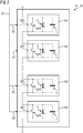
- Fig. 1 shows schematically an electrical circuit 1 of a converter station, which generates a DC voltage (direct voltage) from a three-phase alternating voltage of an alternating current network.
- the three phases P1, P2, P3 of the alternating current network are connected to a transformer T on the primary side.
- the three phases P1, P2, P3 can be connected to the transformer T and disconnected from the transformer T via a main switch ACS.
- the three secondary windings W1, W2, W3 of the transformer T are connected in a star connection here.
- the windings W1, W2, W3 are each connected to one of three AC connections AC on the input side (or correspondingly AC1, AC2, AC3 for the three individual AC connections) of a multi-phase multi-stage converter MMC, the output side is two common DC connected to direct current busbars - Has DC connections (or correspondingly DC +, DC-) at which a DC voltage (as a voltage supply) is available.
- the DC connection DC + is the positive pole and the DC connection DC- is the negative pole of the DC voltage.
- the MMC converter has three phase modules PM1, PM2, PM3, each with one of the three AC connections AC1, AC2, AC3.
- the phase modules PM1, PM2, PM3 are connected in parallel and connected to the two common DC connections DC +, DC-.
- Each phase module PM1, PM2, PM3 comprises two series-connected converter modules UL, UH (or correspondingly UL1, UH1, UL2, UH2, UL3, UH3; for the bipole configuration shown here, H stands for high and L for low), each over an inductance L are connected to one of the two DC connections DC +, DC- and between which the AC connection AC1, AC2, AC3 is arranged.
- Fig. 2 shows schematically that each converter module UL, UH is formed from a plurality of two-pole sub-modules SM connected electrically in series.
- the sub-modules SM have controlled semiconductor switches HS, which here are formed from power semiconductor components IGBT (Insulated Gate Bipolar Transistor).
- the semiconductor switches HS are also designed in a full bridge circuit (VSC full bridge circuit, VSC: Voltage Sourced Converter), but can also be designed in a half bridge circuit (VSC half bridge circuit).
- VSC full bridge circuit VSC: Voltage Sourced Converter
- VSC half bridge circuit there is an energy store C in each case in the form of a capacitor, which can be charged and discharged by the semiconductor switches HS.
- a bypass switch BS short-circuits the sub-module SM when an associated sub-module limit voltage (the first limit voltage) is exceeded.
- the semiconductor switches HS of the sub-module SM can be opened (blocked) via a signal input SBS for a blocking signal BS.
- Fig. 3 shows a sub-module SM with special power semiconductor components IGBT (Insulated Gate Bipolar Transistor) in a full bridge circuit; Fig. 4 in half-bridge circuit.
- IGBT Insulated Gate Bipolar Transistor
- a module arrester MA is connected in parallel to each converter module UL, UH, which, as a surge arrester, limits the converter voltage VU, i.e. the voltage at the converter module, when a converter module limit voltage (the second limit voltage) is exceeded in the manner of a valve by the module arrester MA operates above the second limit voltage in the blocking mode and below the second limit voltage in the forward mode, in which a current that limits the converter voltage VU flows through the module arrester MA.
- a current sensor SIH, SIL (or according to SIH1, SIH2, SIH3, SIL1, SIL2, SIL3) of the multi-stage converter MMC detects the current IH, IL (or according to IH1, IH2, IH3, IL1, IL2, flowing through the respective converter module UL, UH) IL3).
- the current IH, IL of the current sensors SIH, SIL is monitored by a monitoring unit UE.
- the monitoring unit UE In the event of a fault, e.g. serious short-circuits inside the converter, the monitoring unit UE outputs blocking signals BS to the sub-modules SM and a switch-off signal ESOF to the AC circuit breaker ACS, so that all semiconductor switches HS of the sub-modules and the AC circuit breaker ACS are opened .
- the AC voltage AC1, AC2, AC3 i.e. a voltage difference
- the converter modules UL, UH for example for approx. 120 ms.
- the energy stores C of the sub-modules SM are charged, whereby the voltage VU on the converter module UL, UH and correspondingly on the sub-modules SM increases.
- Exceeding the submodule limit voltage due to overcharging is prevented by the module arrester MA, which does not allow the voltage on the converter module UM to rise above the converter module limit voltage, which divided by the number of sub-modules SM of the converter module UM is less than the submodule limit voltage so that the bypass switches BS do not trigger in the time until the AC circuit breaker ACS opens, ie the module arrester MA no longer leads to a failure of sub-modules SM by igniting the bypass switches BS as a result of overloading.
- the module arrester is electrically designed in such a way that almost no currents flow into the module arrester until the point in time of blocking and at the same time the submodule limit voltage (the maximum permitted transient voltage) per submodule SM is not exceeded. From the point of blocking on, the MA modular arrester converts the associated energy into heat in the shortest possible time. Due to the small voltage gap between the voltage at the time of blocking and the limit voltage, it is implemented with a High Cooling Arrester (HCA).
- HCA High Cooling Arrester
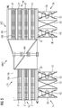
- Fig. 5 shows a front view of the structural arrangement of a converter module UM, which is formed from two converter towers UT1, UT2.
- Each converter tower UT1, UT2 has a support structure SK at the bottom for the electrically insulated support of a vertical frame structure RK with floors ET arranged one above the other on a solid base.
- the frame construction RK has based on Fig. 5 on the left side over three floors ET and on the right side over four floors ET, in each of which sub-modules SM of the converter module UM are arranged side by side according to the sequence in the series connection and are electrically connected to each other.
- the sub-module rows of immediately adjacent floors of an individual converter tower UT1, UT2 and the two converter towers UT1 and UT2 are likewise electrically connected accordingly to form the overall series circuit.
- tubular frames RR as a shield.
- the support structure has support elements SE and tension ropes SS, which give the support structure SK sufficient stability and elasticity against vibrations.
- a coolant is fed to the sub-modules SM for cooling via hoses KS.
- a module arrester MA is arranged between the two converter towers UT1, UT2, here, for example, in a suspended design; In principle, a standing version is also possible.
- the modular arrester MA is designed as a high cooling arrester (surge arrester) and therefore without a housing for better cooling and thus to improve its thermal stability.
- Fig. 6 shows the to Fig. 5 Corresponding top view of the converter module UM with the two converter towers UT1, UT2 and the module arrester MA. It can be seen that each of the converter towers UT1, UT2 is constructed from two half towers UT1a, UT1b, UT2a, UT2b.
- the two converter towers UT1, UT2 are arranged side by side.
- the module arrester MA is located on the side immediately next to each of the two converter towers UT1, UT2 and here with two converter towers UT1, UT2 directly between the two converter towers UT1, UT2.
- Immediately next to a converter tower UT1, UT2 in the sense that no further electrical components are arranged between them.
Landscapes
- Engineering & Computer Science (AREA)
- Power Engineering (AREA)
- Inverter Devices (AREA)
- Rectifiers (AREA)
Priority Applications (1)
| Application Number | Priority Date | Filing Date | Title |
|---|---|---|---|
| PL17715728T PL3580839T3 (pl) | 2017-04-05 | 2017-04-05 | Wielofazowy przekształtnik wielostopniowy |
Applications Claiming Priority (1)
| Application Number | Priority Date | Filing Date | Title |
|---|---|---|---|
| PCT/EP2017/058099 WO2018184671A1 (de) | 2017-04-05 | 2017-04-05 | Mehrphasiger mehrstufenstromrichter |
Publications (2)
| Publication Number | Publication Date |
|---|---|
| EP3580839A1 EP3580839A1 (de) | 2019-12-18 |
| EP3580839B1 true EP3580839B1 (de) | 2021-01-27 |
Family
ID=58489356
Family Applications (1)
| Application Number | Title | Priority Date | Filing Date |
|---|---|---|---|
| EP17715728.6A Active EP3580839B1 (de) | 2017-04-05 | 2017-04-05 | Mehrphasiger mehrstufenstromrichter |
Country Status (6)
| Country | Link |
|---|---|
| US (1) | US10811994B2 (pl) |
| EP (1) | EP3580839B1 (pl) |
| CN (1) | CN211670775U (pl) |
| ES (1) | ES2865202T3 (pl) |
| PL (1) | PL3580839T3 (pl) |
| WO (1) | WO2018184671A1 (pl) |
Families Citing this family (7)
| Publication number | Priority date | Publication date | Assignee | Title |
|---|---|---|---|---|
| EP3627685B1 (en) * | 2017-05-18 | 2022-10-19 | Mitsubishi Electric Corporation | Reactive power compensation device and method for controlling same |
| PL3788707T3 (pl) * | 2018-06-19 | 2023-02-06 | Siemens Energy Global GmbH & Co. KG | System wyrównywania potencjałów dla modułowego przekształtnika - wielopoziomowego |
| WO2020043263A1 (de) * | 2018-08-27 | 2020-03-05 | Siemens Aktiengesellschaft | Mehrphasiger mehrstufenstromrichter mit einer ansteuerung und einem passiven frequenzfilter und verfahren zur ansteuerung des mehrphasigen mehrstufenstromrichters |
| CN114189135A (zh) * | 2021-11-10 | 2022-03-15 | 许继电气股份有限公司 | 具备过压抑制功能的换流阀桥臂子模块及其控制方法、换流阀 |
| EP4526911B1 (en) * | 2022-05-16 | 2026-03-25 | Hitachi Energy Ltd | High voltage bypass device, voltage source converter and operating method |
| CN114915154B (zh) * | 2022-06-14 | 2024-11-29 | 国网智能电网研究院有限公司 | 一种可恢复旁路开关取能电路及分闸控制方法 |
| DE102022125675A1 (de) * | 2022-10-05 | 2024-04-11 | Maschinenfabrik Reinhausen Gmbh | Kombinierte Erdungs- und Schutzeinrichtung für einen modular aufgebauten Spannungs- und Leistungswandler |
Family Cites Families (13)
| Publication number | Priority date | Publication date | Assignee | Title |
|---|---|---|---|---|
| US4710850A (en) | 1986-02-19 | 1987-12-01 | Siemens Aktiengesellschaft | Tower design for high-voltage systems |
| US8570779B2 (en) * | 2007-03-13 | 2013-10-29 | Siemens Aktiengesellschaft | Method for limiting damage to a converter having power semiconductors in the case of a short circuit in the DC voltage intermediate circuit |
| US20140226374A1 (en) * | 2011-07-29 | 2014-08-14 | Abb Technology Ag | Ctl cell protection |
| CN103947099B (zh) * | 2011-11-15 | 2017-04-05 | 阿尔斯通技术有限公司 | 功率电子模块 |
| EP2595302A1 (en) * | 2011-11-21 | 2013-05-22 | ABB Technology AG | Method and device for servicing individual power module during operation of a modular multicell converter |
| CN103063903B (zh) * | 2012-12-10 | 2014-02-19 | 国网智能电网研究院 | 一种模块化多电平换流器过电压计算方法 |
| EP3107172B1 (en) * | 2014-02-14 | 2022-06-01 | Mitsubishi Electric Corporation | Protection system for dc power transmission system, ac/dc converter, and dc power transmission system breaking method |
| EP3068008B1 (en) * | 2015-03-12 | 2020-04-29 | General Electric Technology GmbH | Improvements in or relating to hvdc power converters |
| DE102015109466A1 (de) * | 2015-06-15 | 2016-12-15 | Ge Energy Power Conversion Technology Limited | Stromrichter-Submodul mit Kurzschlusseinrichtung und Stromrichter mit diesem |
| JP5985089B1 (ja) * | 2015-06-23 | 2016-09-06 | 三菱電機株式会社 | 電力変換装置 |
| WO2017077983A1 (ja) * | 2015-11-04 | 2017-05-11 | 三菱電機株式会社 | 電力変換装置 |
| US10855168B2 (en) * | 2016-03-28 | 2020-12-01 | Mitsubishi Electric Corporation | Power conversion device having bypass circuit protection |
| US10790761B2 (en) * | 2017-02-27 | 2020-09-29 | Mitsubishi Electric Corporation | Power conversion device and DC power transmission system |
-
2017
- 2017-04-05 EP EP17715728.6A patent/EP3580839B1/de active Active
- 2017-04-05 CN CN201790001641.6U patent/CN211670775U/zh active Active
- 2017-04-05 PL PL17715728T patent/PL3580839T3/pl unknown
- 2017-04-05 WO PCT/EP2017/058099 patent/WO2018184671A1/de not_active Ceased
- 2017-04-05 US US16/603,326 patent/US10811994B2/en active Active
- 2017-04-05 ES ES17715728T patent/ES2865202T3/es active Active
Also Published As
| Publication number | Publication date |
|---|---|
| EP3580839A1 (de) | 2019-12-18 |
| PL3580839T3 (pl) | 2021-07-19 |
| ES2865202T3 (es) | 2021-10-15 |
| US20200044580A1 (en) | 2020-02-06 |
| WO2018184671A1 (de) | 2018-10-11 |
| US10811994B2 (en) | 2020-10-20 |
| CN211670775U (zh) | 2020-10-13 |
Similar Documents
| Publication | Publication Date | Title |
|---|---|---|
| EP3580839B1 (de) | Mehrphasiger mehrstufenstromrichter | |
| EP3259839B1 (de) | Umrichteranordnung sowie verfahren zu deren kurzschlussschutz | |
| EP2100368B1 (de) | Halbleiterschutzelemente zur beherrschung von dc-seitigen kurzschlüssen bei spannungszwischenkreisumrichtern | |
| EP3211784B1 (de) | Doppel-submodul für einen modularen mehrpunktstromrichter und modularer mehrpunktstromrichter mit diesem | |
| EP2338214A1 (de) | Vorrichtung mit einem umrichter | |
| EP2707944B1 (de) | Hybridumrichter und verfahren zu seiner regelung | |
| US8873258B2 (en) | Method for inhibiting a converter with distributed energy stores | |
| DE10333798B4 (de) | Verfahren zum Kurzschliessen eines fehlerhaften Teilumrichters | |
| WO2009043186A2 (de) | Anordnung zum schutz von wechselrichtern mit spannungszwischenkreis gegen brückenkurzschluss | |
| EP3783783A1 (de) | Anordnung zum regeln eines leistungsflusses in einem wechselspannungsnetz und verfahren zum schutz der anordnung | |
| DE212015000322U1 (de) | Multilevelumrichter mit Redundanzmodul | |
| DE102017220599A1 (de) | Umrichteranordnung zum Stabilisieren eines Wechselspannungsnetzes | |
| EP3639360B1 (de) | Umrichteranordnung mit phasenmodulableiter sowie verfahren zu deren kurzschlussschutz | |
| DE102013213986B4 (de) | Dreipunkt-Stromrichter | |
| WO2018113926A1 (de) | Stromrichter | |
| EP3830921B1 (de) | Sternpunkterdung mit überspannungsbegrenzung für einen mehrphasigen transformator | |
| EP3656033B1 (de) | Stromrichter-anordnung zur anbindung von windenergieanlagen an ein energieversorgungsnetz | |
| DE202020101757U1 (de) | Sicherungsanordnung in MMC-Zelle | |
| WO2020011331A1 (de) | Modularer multilevel-stromrichter mit unterschiedlichen submodultypen | |
| WO2019042566A1 (de) | Umrichteranordnung | |
| WO2025176547A1 (de) | Trafoloser umrichter mit schutz vor erdschlussfehlern | |
| EP4607730A1 (de) | Trafoloser umrichter mit schutz vor erdschlussfehlern | |
| WO2014114339A1 (de) | Modularer mehrstufenumrichter mit schutzableiter | |
| EP4457925A1 (de) | Modul eines modularen multilevelstromrichters |
Legal Events
| Date | Code | Title | Description |
|---|---|---|---|
| STAA | Information on the status of an ep patent application or granted ep patent |
Free format text: STATUS: UNKNOWN |
|
| STAA | Information on the status of an ep patent application or granted ep patent |
Free format text: STATUS: THE INTERNATIONAL PUBLICATION HAS BEEN MADE |
|
| PUAI | Public reference made under article 153(3) epc to a published international application that has entered the european phase |
Free format text: ORIGINAL CODE: 0009012 |
|
| STAA | Information on the status of an ep patent application or granted ep patent |
Free format text: STATUS: REQUEST FOR EXAMINATION WAS MADE |
|
| 17P | Request for examination filed |
Effective date: 20190909 |
|
| AK | Designated contracting states |
Kind code of ref document: A1 Designated state(s): AL AT BE BG CH CY CZ DE DK EE ES FI FR GB GR HR HU IE IS IT LI LT LU LV MC MK MT NL NO PL PT RO RS SE SI SK SM TR |
|
| AX | Request for extension of the european patent |
Extension state: BA ME |
|
| DAV | Request for validation of the european patent (deleted) | ||
| DAX | Request for extension of the european patent (deleted) | ||
| GRAP | Despatch of communication of intention to grant a patent |
Free format text: ORIGINAL CODE: EPIDOSNIGR1 |
|
| STAA | Information on the status of an ep patent application or granted ep patent |
Free format text: STATUS: GRANT OF PATENT IS INTENDED |
|
| INTG | Intention to grant announced |
Effective date: 20200821 |
|
| GRAS | Grant fee paid |
Free format text: ORIGINAL CODE: EPIDOSNIGR3 |
|
| GRAA | (expected) grant |
Free format text: ORIGINAL CODE: 0009210 |
|
| STAA | Information on the status of an ep patent application or granted ep patent |
Free format text: STATUS: THE PATENT HAS BEEN GRANTED |
|
| AK | Designated contracting states |
Kind code of ref document: B1 Designated state(s): AL AT BE BG CH CY CZ DE DK EE ES FI FR GB GR HR HU IE IS IT LI LT LU LV MC MK MT NL NO PL PT RO RS SE SI SK SM TR |
|
| RAP1 | Party data changed (applicant data changed or rights of an application transferred) |
Owner name: SIEMENS ENERGY GLOBAL GMBH & CO. KG |
|
| REG | Reference to a national code |
Ref country code: GB Ref legal event code: FG4D Free format text: NOT ENGLISH |
|
| REG | Reference to a national code |
Ref country code: CH Ref legal event code: EP |
|
| REG | Reference to a national code |
Ref country code: AT Ref legal event code: REF Ref document number: 1359226 Country of ref document: AT Kind code of ref document: T Effective date: 20210215 |
|
| REG | Reference to a national code |
Ref country code: IE Ref legal event code: FG4D Free format text: LANGUAGE OF EP DOCUMENT: GERMAN |
|
| REG | Reference to a national code |
Ref country code: DE Ref legal event code: R096 Ref document number: 502017009232 Country of ref document: DE |
|
| REG | Reference to a national code |
Ref country code: SE Ref legal event code: TRGR |
|
| REG | Reference to a national code |
Ref country code: NL Ref legal event code: MP Effective date: 20210127 |
|
| REG | Reference to a national code |
Ref country code: LT Ref legal event code: MG9D |
|
| PG25 | Lapsed in a contracting state [announced via postgrant information from national office to epo] |
Ref country code: GR Free format text: LAPSE BECAUSE OF FAILURE TO SUBMIT A TRANSLATION OF THE DESCRIPTION OR TO PAY THE FEE WITHIN THE PRESCRIBED TIME-LIMIT Effective date: 20210428 Ref country code: FI Free format text: LAPSE BECAUSE OF FAILURE TO SUBMIT A TRANSLATION OF THE DESCRIPTION OR TO PAY THE FEE WITHIN THE PRESCRIBED TIME-LIMIT Effective date: 20210127 Ref country code: HR Free format text: LAPSE BECAUSE OF FAILURE TO SUBMIT A TRANSLATION OF THE DESCRIPTION OR TO PAY THE FEE WITHIN THE PRESCRIBED TIME-LIMIT Effective date: 20210127 Ref country code: PT Free format text: LAPSE BECAUSE OF FAILURE TO SUBMIT A TRANSLATION OF THE DESCRIPTION OR TO PAY THE FEE WITHIN THE PRESCRIBED TIME-LIMIT Effective date: 20210527 Ref country code: NO Free format text: LAPSE BECAUSE OF FAILURE TO SUBMIT A TRANSLATION OF THE DESCRIPTION OR TO PAY THE FEE WITHIN THE PRESCRIBED TIME-LIMIT Effective date: 20210427 Ref country code: LT Free format text: LAPSE BECAUSE OF FAILURE TO SUBMIT A TRANSLATION OF THE DESCRIPTION OR TO PAY THE FEE WITHIN THE PRESCRIBED TIME-LIMIT Effective date: 20210127 Ref country code: BG Free format text: LAPSE BECAUSE OF FAILURE TO SUBMIT A TRANSLATION OF THE DESCRIPTION OR TO PAY THE FEE WITHIN THE PRESCRIBED TIME-LIMIT Effective date: 20210427 |
|
| PG25 | Lapsed in a contracting state [announced via postgrant information from national office to epo] |
Ref country code: RS Free format text: LAPSE BECAUSE OF FAILURE TO SUBMIT A TRANSLATION OF THE DESCRIPTION OR TO PAY THE FEE WITHIN THE PRESCRIBED TIME-LIMIT Effective date: 20210127 Ref country code: LV Free format text: LAPSE BECAUSE OF FAILURE TO SUBMIT A TRANSLATION OF THE DESCRIPTION OR TO PAY THE FEE WITHIN THE PRESCRIBED TIME-LIMIT Effective date: 20210127 |
|
| PG25 | Lapsed in a contracting state [announced via postgrant information from national office to epo] |
Ref country code: IS Free format text: LAPSE BECAUSE OF FAILURE TO SUBMIT A TRANSLATION OF THE DESCRIPTION OR TO PAY THE FEE WITHIN THE PRESCRIBED TIME-LIMIT Effective date: 20210527 |
|
| REG | Reference to a national code |
Ref country code: ES Ref legal event code: FG2A Ref document number: 2865202 Country of ref document: ES Kind code of ref document: T3 Effective date: 20211015 |
|
| REG | Reference to a national code |
Ref country code: DE Ref legal event code: R097 Ref document number: 502017009232 Country of ref document: DE |
|
| PG25 | Lapsed in a contracting state [announced via postgrant information from national office to epo] |
Ref country code: SM Free format text: LAPSE BECAUSE OF FAILURE TO SUBMIT A TRANSLATION OF THE DESCRIPTION OR TO PAY THE FEE WITHIN THE PRESCRIBED TIME-LIMIT Effective date: 20210127 Ref country code: EE Free format text: LAPSE BECAUSE OF FAILURE TO SUBMIT A TRANSLATION OF THE DESCRIPTION OR TO PAY THE FEE WITHIN THE PRESCRIBED TIME-LIMIT Effective date: 20210127 Ref country code: CZ Free format text: LAPSE BECAUSE OF FAILURE TO SUBMIT A TRANSLATION OF THE DESCRIPTION OR TO PAY THE FEE WITHIN THE PRESCRIBED TIME-LIMIT Effective date: 20210127 |
|
| PG25 | Lapsed in a contracting state [announced via postgrant information from national office to epo] |
Ref country code: MC Free format text: LAPSE BECAUSE OF FAILURE TO SUBMIT A TRANSLATION OF THE DESCRIPTION OR TO PAY THE FEE WITHIN THE PRESCRIBED TIME-LIMIT Effective date: 20210127 Ref country code: RO Free format text: LAPSE BECAUSE OF FAILURE TO SUBMIT A TRANSLATION OF THE DESCRIPTION OR TO PAY THE FEE WITHIN THE PRESCRIBED TIME-LIMIT Effective date: 20210127 Ref country code: DK Free format text: LAPSE BECAUSE OF FAILURE TO SUBMIT A TRANSLATION OF THE DESCRIPTION OR TO PAY THE FEE WITHIN THE PRESCRIBED TIME-LIMIT Effective date: 20210127 Ref country code: SK Free format text: LAPSE BECAUSE OF FAILURE TO SUBMIT A TRANSLATION OF THE DESCRIPTION OR TO PAY THE FEE WITHIN THE PRESCRIBED TIME-LIMIT Effective date: 20210127 |
|
| PLBE | No opposition filed within time limit |
Free format text: ORIGINAL CODE: 0009261 |
|
| STAA | Information on the status of an ep patent application or granted ep patent |
Free format text: STATUS: NO OPPOSITION FILED WITHIN TIME LIMIT |
|
| PG25 | Lapsed in a contracting state [announced via postgrant information from national office to epo] |
Ref country code: LU Free format text: LAPSE BECAUSE OF NON-PAYMENT OF DUE FEES Effective date: 20210405 |
|
| 26N | No opposition filed |
Effective date: 20211028 |
|
| REG | Reference to a national code |
Ref country code: BE Ref legal event code: MM Effective date: 20210430 |
|
| PG25 | Lapsed in a contracting state [announced via postgrant information from national office to epo] |
Ref country code: LI Free format text: LAPSE BECAUSE OF NON-PAYMENT OF DUE FEES Effective date: 20210430 Ref country code: CH Free format text: LAPSE BECAUSE OF NON-PAYMENT OF DUE FEES Effective date: 20210430 Ref country code: AL Free format text: LAPSE BECAUSE OF FAILURE TO SUBMIT A TRANSLATION OF THE DESCRIPTION OR TO PAY THE FEE WITHIN THE PRESCRIBED TIME-LIMIT Effective date: 20210127 |
|
| PG25 | Lapsed in a contracting state [announced via postgrant information from national office to epo] |
Ref country code: SI Free format text: LAPSE BECAUSE OF FAILURE TO SUBMIT A TRANSLATION OF THE DESCRIPTION OR TO PAY THE FEE WITHIN THE PRESCRIBED TIME-LIMIT Effective date: 20210127 |
|
| PG25 | Lapsed in a contracting state [announced via postgrant information from national office to epo] |
Ref country code: IE Free format text: LAPSE BECAUSE OF NON-PAYMENT OF DUE FEES Effective date: 20210405 |
|
| PG25 | Lapsed in a contracting state [announced via postgrant information from national office to epo] |
Ref country code: IS Free format text: LAPSE BECAUSE OF FAILURE TO SUBMIT A TRANSLATION OF THE DESCRIPTION OR TO PAY THE FEE WITHIN THE PRESCRIBED TIME-LIMIT Effective date: 20210527 |
|
| PG25 | Lapsed in a contracting state [announced via postgrant information from national office to epo] |
Ref country code: BE Free format text: LAPSE BECAUSE OF NON-PAYMENT OF DUE FEES Effective date: 20210430 |
|
| REG | Reference to a national code |
Ref country code: AT Ref legal event code: MM01 Ref document number: 1359226 Country of ref document: AT Kind code of ref document: T Effective date: 20220405 |
|
| PG25 | Lapsed in a contracting state [announced via postgrant information from national office to epo] |
Ref country code: NL Free format text: LAPSE BECAUSE OF NON-PAYMENT OF DUE FEES Effective date: 20210127 Ref country code: CY Free format text: LAPSE BECAUSE OF FAILURE TO SUBMIT A TRANSLATION OF THE DESCRIPTION OR TO PAY THE FEE WITHIN THE PRESCRIBED TIME-LIMIT Effective date: 20210127 |
|
| PG25 | Lapsed in a contracting state [announced via postgrant information from national office to epo] |
Ref country code: HU Free format text: LAPSE BECAUSE OF FAILURE TO SUBMIT A TRANSLATION OF THE DESCRIPTION OR TO PAY THE FEE WITHIN THE PRESCRIBED TIME-LIMIT; INVALID AB INITIO Effective date: 20170405 Ref country code: AT Free format text: LAPSE BECAUSE OF NON-PAYMENT OF DUE FEES Effective date: 20220405 |
|
| P01 | Opt-out of the competence of the unified patent court (upc) registered |
Effective date: 20231222 |
|
| PG25 | Lapsed in a contracting state [announced via postgrant information from national office to epo] |
Ref country code: MK Free format text: LAPSE BECAUSE OF FAILURE TO SUBMIT A TRANSLATION OF THE DESCRIPTION OR TO PAY THE FEE WITHIN THE PRESCRIBED TIME-LIMIT Effective date: 20210127 |
|
| PG25 | Lapsed in a contracting state [announced via postgrant information from national office to epo] |
Ref country code: TR Free format text: LAPSE BECAUSE OF FAILURE TO SUBMIT A TRANSLATION OF THE DESCRIPTION OR TO PAY THE FEE WITHIN THE PRESCRIBED TIME-LIMIT Effective date: 20210127 |
|
| PG25 | Lapsed in a contracting state [announced via postgrant information from national office to epo] |
Ref country code: MT Free format text: LAPSE BECAUSE OF FAILURE TO SUBMIT A TRANSLATION OF THE DESCRIPTION OR TO PAY THE FEE WITHIN THE PRESCRIBED TIME-LIMIT Effective date: 20210127 |
|
| PGFP | Annual fee paid to national office [announced via postgrant information from national office to epo] |
Ref country code: PL Payment date: 20250312 Year of fee payment: 9 |
|
| PGFP | Annual fee paid to national office [announced via postgrant information from national office to epo] |
Ref country code: DE Payment date: 20250428 Year of fee payment: 9 |
|
| PGFP | Annual fee paid to national office [announced via postgrant information from national office to epo] |
Ref country code: ES Payment date: 20250513 Year of fee payment: 9 Ref country code: GB Payment date: 20250422 Year of fee payment: 9 |
|
| PGFP | Annual fee paid to national office [announced via postgrant information from national office to epo] |
Ref country code: IT Payment date: 20250422 Year of fee payment: 9 |
|
| PGFP | Annual fee paid to national office [announced via postgrant information from national office to epo] |
Ref country code: FR Payment date: 20250424 Year of fee payment: 9 |
|
| PGFP | Annual fee paid to national office [announced via postgrant information from national office to epo] |
Ref country code: SE Payment date: 20250424 Year of fee payment: 9 |