EP3579669A2 - Deformed layer for short electric connection between structures of electric device - Google Patents
Deformed layer for short electric connection between structures of electric device Download PDFInfo
- Publication number
- EP3579669A2 EP3579669A2 EP19178671.4A EP19178671A EP3579669A2 EP 3579669 A2 EP3579669 A2 EP 3579669A2 EP 19178671 A EP19178671 A EP 19178671A EP 3579669 A2 EP3579669 A2 EP 3579669A2
- Authority
- EP
- European Patent Office
- Prior art keywords
- deformed layer
- electric device
- layer
- deformed
- electric
- Prior art date
- Legal status (The legal status is an assumption and is not a legal conclusion. Google has not performed a legal analysis and makes no representation as to the accuracy of the status listed.)
- Pending
Links
Images

Classifications
-
- H—ELECTRICITY
- H01—ELECTRIC ELEMENTS
- H01R—ELECTRICALLY-CONDUCTIVE CONNECTIONS; STRUCTURAL ASSOCIATIONS OF A PLURALITY OF MUTUALLY-INSULATED ELECTRICAL CONNECTING ELEMENTS; COUPLING DEVICES; CURRENT COLLECTORS
- H01R12/00—Structural associations of a plurality of mutually-insulated electrical connecting elements, specially adapted for printed circuits, e.g. printed circuit boards [PCB], flat or ribbon cables, or like generally planar structures, e.g. terminal strips, terminal blocks; Coupling devices specially adapted for printed circuits, flat or ribbon cables, or like generally planar structures; Terminals specially adapted for contact with, or insertion into, printed circuits, flat or ribbon cables, or like generally planar structures
- H01R12/50—Fixed connections
- H01R12/59—Fixed connections for flexible printed circuits, flat or ribbon cables or like structures
- H01R12/61—Fixed connections for flexible printed circuits, flat or ribbon cables or like structures connecting to flexible printed circuits, flat or ribbon cables or like structures
-
- H—ELECTRICITY
- H10—SEMICONDUCTOR DEVICES; ELECTRIC SOLID-STATE DEVICES NOT OTHERWISE PROVIDED FOR
- H10W—GENERIC PACKAGES, INTERCONNECTIONS, CONNECTORS OR OTHER CONSTRUCTIONAL DETAILS OF DEVICES COVERED BY CLASS H10
- H10W70/00—Package substrates; Interposers; Redistribution layers [RDL]
- H10W70/60—Insulating or insulated package substrates; Interposers; Redistribution layers
- H10W70/67—Insulating or insulated package substrates; Interposers; Redistribution layers characterised by their insulating layers or insulating parts
- H10W70/688—Flexible insulating substrates
-
- H—ELECTRICITY
- H01—ELECTRIC ELEMENTS
- H01R—ELECTRICALLY-CONDUCTIVE CONNECTIONS; STRUCTURAL ASSOCIATIONS OF A PLURALITY OF MUTUALLY-INSULATED ELECTRICAL CONNECTING ELEMENTS; COUPLING DEVICES; CURRENT COLLECTORS
- H01R12/00—Structural associations of a plurality of mutually-insulated electrical connecting elements, specially adapted for printed circuits, e.g. printed circuit boards [PCB], flat or ribbon cables, or like generally planar structures, e.g. terminal strips, terminal blocks; Coupling devices specially adapted for printed circuits, flat or ribbon cables, or like generally planar structures; Terminals specially adapted for contact with, or insertion into, printed circuits, flat or ribbon cables, or like generally planar structures
- H01R12/70—Coupling devices
- H01R12/77—Coupling devices for flexible printed circuits, flat or ribbon cables or like structures
- H01R12/778—Coupling parts carrying sockets, clips or analogous counter-contacts
-
- H—ELECTRICITY
- H01—ELECTRIC ELEMENTS
- H01R—ELECTRICALLY-CONDUCTIVE CONNECTIONS; STRUCTURAL ASSOCIATIONS OF A PLURALITY OF MUTUALLY-INSULATED ELECTRICAL CONNECTING ELEMENTS; COUPLING DEVICES; CURRENT COLLECTORS
- H01R13/00—Details of coupling devices of the kinds covered by groups H01R12/70 or H01R24/00 - H01R33/00
- H01R13/02—Contact members
- H01R13/03—Contact members characterised by the material, e.g. plating, or coating materials
-
- H—ELECTRICITY
- H01—ELECTRIC ELEMENTS
- H01R—ELECTRICALLY-CONDUCTIVE CONNECTIONS; STRUCTURAL ASSOCIATIONS OF A PLURALITY OF MUTUALLY-INSULATED ELECTRICAL CONNECTING ELEMENTS; COUPLING DEVICES; CURRENT COLLECTORS
- H01R31/00—Coupling parts supported only by co-operation with counterpart
- H01R31/06—Intermediate parts for linking two coupling parts, e.g. adapter
-
- H—ELECTRICITY
- H05—ELECTRIC TECHNIQUES NOT OTHERWISE PROVIDED FOR
- H05K—PRINTED CIRCUITS; CASINGS OR CONSTRUCTIONAL DETAILS OF ELECTRIC APPARATUS; MANUFACTURE OF ASSEMBLAGES OF ELECTRICAL COMPONENTS
- H05K1/00—Printed circuits
- H05K1/02—Details
- H05K1/0296—Conductive pattern lay-out details not covered by sub groups H05K1/02 - H05K1/0295
- H05K1/0298—Multilayer circuits
-
- H—ELECTRICITY
- H05—ELECTRIC TECHNIQUES NOT OTHERWISE PROVIDED FOR
- H05K—PRINTED CIRCUITS; CASINGS OR CONSTRUCTIONAL DETAILS OF ELECTRIC APPARATUS; MANUFACTURE OF ASSEMBLAGES OF ELECTRICAL COMPONENTS
- H05K1/00—Printed circuits
- H05K1/02—Details
- H05K1/03—Use of materials for the substrate
- H05K1/0393—Flexible materials
-
- H—ELECTRICITY
- H05—ELECTRIC TECHNIQUES NOT OTHERWISE PROVIDED FOR
- H05K—PRINTED CIRCUITS; CASINGS OR CONSTRUCTIONAL DETAILS OF ELECTRIC APPARATUS; MANUFACTURE OF ASSEMBLAGES OF ELECTRICAL COMPONENTS
- H05K1/00—Printed circuits
- H05K1/18—Printed circuits structurally associated with non-printed electric components
- H05K1/182—Printed circuits structurally associated with non-printed electric components associated with components mounted in printed circuit boards [PCB], e.g. insert-mounted components [IMC]
- H05K1/185—Printed circuits structurally associated with non-printed electric components associated with components mounted in printed circuit boards [PCB], e.g. insert-mounted components [IMC] associated with components encapsulated in the insulating substrate of the PCBs; associated with components incorporated in internal layers of multilayer circuit boards
- H05K1/186—Printed circuits structurally associated with non-printed electric components associated with components mounted in printed circuit boards [PCB], e.g. insert-mounted components [IMC] associated with components encapsulated in the insulating substrate of the PCBs; associated with components incorporated in internal layers of multilayer circuit boards manufactured by mounting on or connecting to patterned circuits before or during embedding
-
- H—ELECTRICITY
- H05—ELECTRIC TECHNIQUES NOT OTHERWISE PROVIDED FOR
- H05K—PRINTED CIRCUITS; CASINGS OR CONSTRUCTIONAL DETAILS OF ELECTRIC APPARATUS; MANUFACTURE OF ASSEMBLAGES OF ELECTRICAL COMPONENTS
- H05K3/00—Apparatus or processes for manufacturing printed circuits
- H05K3/46—Manufacturing multilayer circuits
- H05K3/4602—Manufacturing multilayer circuits characterized by a special circuit board as base or central core whereon additional circuit layers are built or additional circuit boards are laminated
-
- H—ELECTRICITY
- H05—ELECTRIC TECHNIQUES NOT OTHERWISE PROVIDED FOR
- H05K—PRINTED CIRCUITS; CASINGS OR CONSTRUCTIONAL DETAILS OF ELECTRIC APPARATUS; MANUFACTURE OF ASSEMBLAGES OF ELECTRICAL COMPONENTS
- H05K7/00—Constructional details common to different types of electric apparatus
- H05K7/02—Arrangements of circuit components or wiring on supporting structure
- H05K7/026—Multiple connections subassemblies
-
- H—ELECTRICITY
- H10—SEMICONDUCTOR DEVICES; ELECTRIC SOLID-STATE DEVICES NOT OTHERWISE PROVIDED FOR
- H10W—GENERIC PACKAGES, INTERCONNECTIONS, CONNECTORS OR OTHER CONSTRUCTIONAL DETAILS OF DEVICES COVERED BY CLASS H10
- H10W20/00—Interconnections in chips, wafers or substrates
- H10W20/40—Interconnections external to wafers or substrates, e.g. back-end-of-line [BEOL] metallisations or vias connecting to gate electrodes
- H10W20/41—Interconnections external to wafers or substrates, e.g. back-end-of-line [BEOL] metallisations or vias connecting to gate electrodes characterised by their conductive parts
- H10W20/42—Vias, e.g. via plugs
-
- H—ELECTRICITY
- H10—SEMICONDUCTOR DEVICES; ELECTRIC SOLID-STATE DEVICES NOT OTHERWISE PROVIDED FOR
- H10W—GENERIC PACKAGES, INTERCONNECTIONS, CONNECTORS OR OTHER CONSTRUCTIONAL DETAILS OF DEVICES COVERED BY CLASS H10
- H10W44/00—Electrical arrangements for controlling or matching impedance
-
- H—ELECTRICITY
- H10—SEMICONDUCTOR DEVICES; ELECTRIC SOLID-STATE DEVICES NOT OTHERWISE PROVIDED FOR
- H10W—GENERIC PACKAGES, INTERCONNECTIONS, CONNECTORS OR OTHER CONSTRUCTIONAL DETAILS OF DEVICES COVERED BY CLASS H10
- H10W70/00—Package substrates; Interposers; Redistribution layers [RDL]
- H10W70/60—Insulating or insulated package substrates; Interposers; Redistribution layers
- H10W70/611—Insulating or insulated package substrates; Interposers; Redistribution layers for connecting multiple chips together
-
- H—ELECTRICITY
- H10—SEMICONDUCTOR DEVICES; ELECTRIC SOLID-STATE DEVICES NOT OTHERWISE PROVIDED FOR
- H10W—GENERIC PACKAGES, INTERCONNECTIONS, CONNECTORS OR OTHER CONSTRUCTIONAL DETAILS OF DEVICES COVERED BY CLASS H10
- H10W74/00—Encapsulations, e.g. protective coatings
- H10W74/01—Manufacture or treatment
-
- H—ELECTRICITY
- H10—SEMICONDUCTOR DEVICES; ELECTRIC SOLID-STATE DEVICES NOT OTHERWISE PROVIDED FOR
- H10W—GENERIC PACKAGES, INTERCONNECTIONS, CONNECTORS OR OTHER CONSTRUCTIONAL DETAILS OF DEVICES COVERED BY CLASS H10
- H10W74/00—Encapsulations, e.g. protective coatings
- H10W74/10—Encapsulations, e.g. protective coatings characterised by their shape or disposition
- H10W74/131—Encapsulations, e.g. protective coatings characterised by their shape or disposition the semiconductor body being only partially enclosed
-
- H—ELECTRICITY
- H10—SEMICONDUCTOR DEVICES; ELECTRIC SOLID-STATE DEVICES NOT OTHERWISE PROVIDED FOR
- H10W—GENERIC PACKAGES, INTERCONNECTIONS, CONNECTORS OR OTHER CONSTRUCTIONAL DETAILS OF DEVICES COVERED BY CLASS H10
- H10W90/00—Package configurations
- H10W90/401—Package configurations characterised by multiple insulating or insulated package substrates, interposers or RDLs
-
- H—ELECTRICITY
- H05—ELECTRIC TECHNIQUES NOT OTHERWISE PROVIDED FOR
- H05K—PRINTED CIRCUITS; CASINGS OR CONSTRUCTIONAL DETAILS OF ELECTRIC APPARATUS; MANUFACTURE OF ASSEMBLAGES OF ELECTRICAL COMPONENTS
- H05K1/00—Printed circuits
- H05K1/18—Printed circuits structurally associated with non-printed electric components
- H05K1/189—Printed circuits structurally associated with non-printed electric components characterised by the use of flexible or folded printed circuits
-
- H—ELECTRICITY
- H05—ELECTRIC TECHNIQUES NOT OTHERWISE PROVIDED FOR
- H05K—PRINTED CIRCUITS; CASINGS OR CONSTRUCTIONAL DETAILS OF ELECTRIC APPARATUS; MANUFACTURE OF ASSEMBLAGES OF ELECTRICAL COMPONENTS
- H05K2201/00—Indexing scheme relating to printed circuits covered by H05K1/00
- H05K2201/01—Dielectrics
- H05K2201/0104—Properties and characteristics in general
- H05K2201/0129—Thermoplastic polymer, e.g. auto-adhesive layer; Shaping of thermoplastic polymer
-
- H—ELECTRICITY
- H05—ELECTRIC TECHNIQUES NOT OTHERWISE PROVIDED FOR
- H05K—PRINTED CIRCUITS; CASINGS OR CONSTRUCTIONAL DETAILS OF ELECTRIC APPARATUS; MANUFACTURE OF ASSEMBLAGES OF ELECTRICAL COMPONENTS
- H05K2201/00—Indexing scheme relating to printed circuits covered by H05K1/00
- H05K2201/05—Flexible printed circuits [FPCs]
- H05K2201/056—Folded around rigid support or component
-
- H—ELECTRICITY
- H05—ELECTRIC TECHNIQUES NOT OTHERWISE PROVIDED FOR
- H05K—PRINTED CIRCUITS; CASINGS OR CONSTRUCTIONAL DETAILS OF ELECTRIC APPARATUS; MANUFACTURE OF ASSEMBLAGES OF ELECTRICAL COMPONENTS
- H05K2201/00—Indexing scheme relating to printed circuits covered by H05K1/00
- H05K2201/09—Shape and layout
- H05K2201/09009—Substrate related
- H05K2201/091—Locally and permanently deformed areas including dielectric material
-
- H—ELECTRICITY
- H05—ELECTRIC TECHNIQUES NOT OTHERWISE PROVIDED FOR
- H05K—PRINTED CIRCUITS; CASINGS OR CONSTRUCTIONAL DETAILS OF ELECTRIC APPARATUS; MANUFACTURE OF ASSEMBLAGES OF ELECTRICAL COMPONENTS
- H05K2201/00—Indexing scheme relating to printed circuits covered by H05K1/00
- H05K2201/09—Shape and layout
- H05K2201/09209—Shape and layout details of conductors
- H05K2201/095—Conductive through-holes or vias
- H05K2201/09509—Blind vias, i.e. vias having one side closed
-
- H—ELECTRICITY
- H05—ELECTRIC TECHNIQUES NOT OTHERWISE PROVIDED FOR
- H05K—PRINTED CIRCUITS; CASINGS OR CONSTRUCTIONAL DETAILS OF ELECTRIC APPARATUS; MANUFACTURE OF ASSEMBLAGES OF ELECTRICAL COMPONENTS
- H05K3/00—Apparatus or processes for manufacturing printed circuits
- H05K3/46—Manufacturing multilayer circuits
- H05K3/4611—Manufacturing multilayer circuits by laminating two or more circuit boards
- H05K3/4614—Manufacturing multilayer circuits by laminating two or more circuit boards the electrical connections between the circuit boards being made during lamination
-
- H—ELECTRICITY
- H05—ELECTRIC TECHNIQUES NOT OTHERWISE PROVIDED FOR
- H05K—PRINTED CIRCUITS; CASINGS OR CONSTRUCTIONAL DETAILS OF ELECTRIC APPARATUS; MANUFACTURE OF ASSEMBLAGES OF ELECTRICAL COMPONENTS
- H05K3/00—Apparatus or processes for manufacturing printed circuits
- H05K3/46—Manufacturing multilayer circuits
- H05K3/4688—Composite multilayer circuits, i.e. comprising insulating layers having different properties
-
- H—ELECTRICITY
- H10—SEMICONDUCTOR DEVICES; ELECTRIC SOLID-STATE DEVICES NOT OTHERWISE PROVIDED FOR
- H10W—GENERIC PACKAGES, INTERCONNECTIONS, CONNECTORS OR OTHER CONSTRUCTIONAL DETAILS OF DEVICES COVERED BY CLASS H10
- H10W70/00—Package substrates; Interposers; Redistribution layers [RDL]
- H10W70/01—Manufacture or treatment
- H10W70/05—Manufacture or treatment of insulating or insulated package substrates, or of interposers, or of redistribution layers
- H10W70/093—Connecting or disconnecting other interconnections thereto or therefrom, e.g. connecting bond wires or bumps
-
- H—ELECTRICITY
- H10—SEMICONDUCTOR DEVICES; ELECTRIC SOLID-STATE DEVICES NOT OTHERWISE PROVIDED FOR
- H10W—GENERIC PACKAGES, INTERCONNECTIONS, CONNECTORS OR OTHER CONSTRUCTIONAL DETAILS OF DEVICES COVERED BY CLASS H10
- H10W70/00—Package substrates; Interposers; Redistribution layers [RDL]
- H10W70/60—Insulating or insulated package substrates; Interposers; Redistribution layers
- H10W70/67—Insulating or insulated package substrates; Interposers; Redistribution layers characterised by their insulating layers or insulating parts
- H10W70/68—Shapes or dispositions thereof
- H10W70/682—Shapes or dispositions thereof comprising holes having chips therein
-
- H—ELECTRICITY
- H10—SEMICONDUCTOR DEVICES; ELECTRIC SOLID-STATE DEVICES NOT OTHERWISE PROVIDED FOR
- H10W—GENERIC PACKAGES, INTERCONNECTIONS, CONNECTORS OR OTHER CONSTRUCTIONAL DETAILS OF DEVICES COVERED BY CLASS H10
- H10W72/00—Interconnections or connectors in packages
- H10W72/90—Bond pads, in general
- H10W72/941—Dispositions of bond pads
- H10W72/9413—Dispositions of bond pads on encapsulations
-
- H—ELECTRICITY
- H10—SEMICONDUCTOR DEVICES; ELECTRIC SOLID-STATE DEVICES NOT OTHERWISE PROVIDED FOR
- H10W—GENERIC PACKAGES, INTERCONNECTIONS, CONNECTORS OR OTHER CONSTRUCTIONAL DETAILS OF DEVICES COVERED BY CLASS H10
- H10W72/00—Interconnections or connectors in packages
- H10W72/90—Bond pads, in general
- H10W72/941—Dispositions of bond pads
- H10W72/944—Dispositions of multiple bond pads
-
- H—ELECTRICITY
- H10—SEMICONDUCTOR DEVICES; ELECTRIC SOLID-STATE DEVICES NOT OTHERWISE PROVIDED FOR
- H10W—GENERIC PACKAGES, INTERCONNECTIONS, CONNECTORS OR OTHER CONSTRUCTIONAL DETAILS OF DEVICES COVERED BY CLASS H10
- H10W74/00—Encapsulations, e.g. protective coatings
- H10W74/10—Encapsulations, e.g. protective coatings characterised by their shape or disposition
- H10W74/111—Encapsulations, e.g. protective coatings characterised by their shape or disposition the semiconductor body being completely enclosed
- H10W74/114—Encapsulations, e.g. protective coatings characterised by their shape or disposition the semiconductor body being completely enclosed by a substrate and the encapsulations
-
- H—ELECTRICITY
- H10—SEMICONDUCTOR DEVICES; ELECTRIC SOLID-STATE DEVICES NOT OTHERWISE PROVIDED FOR
- H10W—GENERIC PACKAGES, INTERCONNECTIONS, CONNECTORS OR OTHER CONSTRUCTIONAL DETAILS OF DEVICES COVERED BY CLASS H10
- H10W90/00—Package configurations
- H10W90/701—Package configurations characterised by the relative positions of pads or connectors relative to package parts
- H10W90/721—Package configurations characterised by the relative positions of pads or connectors relative to package parts of bump connectors
- H10W90/724—Package configurations characterised by the relative positions of pads or connectors relative to package parts of bump connectors between a chip and a stacked insulating package substrate, interposer or RDL
-
- H—ELECTRICITY
- H10—SEMICONDUCTOR DEVICES; ELECTRIC SOLID-STATE DEVICES NOT OTHERWISE PROVIDED FOR
- H10W—GENERIC PACKAGES, INTERCONNECTIONS, CONNECTORS OR OTHER CONSTRUCTIONAL DETAILS OF DEVICES COVERED BY CLASS H10
- H10W90/00—Package configurations
- H10W90/701—Package configurations characterised by the relative positions of pads or connectors relative to package parts
- H10W90/731—Package configurations characterised by the relative positions of pads or connectors relative to package parts of die-attach connectors
- H10W90/734—Package configurations characterised by the relative positions of pads or connectors relative to package parts of die-attach connectors between a chip and a stacked insulating package substrate, interposer or RDL
Definitions
- the invention relates to an electric device and to a method of manufacturing an electric device.
- an electric device which comprises a first structure, a second structure, and a deformed layer comprising a dielectric matrix and electrically conductive elements formed therein, wherein the deformed layer is arranged to electrically couple the first structure with the second structure.
- a method of manufacturing an electric device comprising providing a first structure, providing a second structure, and electrically coupling the first structure with the second structure by a deformed layer comprising a dielectric matrix and electrically conductive elements.
- the term “electric device” may particularly denote any electric member, module or package in which two or more structures are functionally coupled and electrically connected via a deformed layer with electrically conductive elements therein.
- structure may particularly denote an electric structure such as a physical body providing an electric or electronic functionality.
- Examples of such a structure are electronic chips, component carriers, electric packages or modules, etc.
- the term "deformed layer” may particularly denote a curved, bent or otherwise three-dimensionally deformed layer which is deformed in such a way as to provide a shortened electric connection between structures via electrically conductive elements integrated within the deformed layer.
- the deformed layer may have a plurality of connected portions, wherein one or more of the portions may extend horizontally and one or more other of the portions may extend vertically.
- an electric device in which two or more (in particular electric) structures are electrically connected at least partially by a deformed layer having integrated electrically conductive elements.
- a deformed layer having integrated electrically conductive elements.
- z-axis coupling of a plate shaped electric device may be accomplished very efficiently in this way.
- a highly compact electric device with short current paths can be provided allowing for an efficient and low-loss transport of electric signals and/or electric energy between the structures via the deformed layer.
- a circuit designer In view of the freely deformable shape of the deformed layer, it is possible for a circuit designer to highly flexibly establish substantially any desired coupling architecture by correspondingly bending the deformed layer.
- the deformed layer is a thermo-deformed layer or thermally deformed layer (for instance comprising a thermoplastic material).
- the term "thermally deformed” or “thermo-deformed” layer may particularly denote a layer processed by thermoforming.
- a thermally deformed layer may be the result of a manufacturing process in which a sheet of an appropriate material (for instance a dielectric (in particular plastic) sheet with embedded electrically conductive elements is heated to a pliable forming temperature, formed to a specific shape in a mold, and trimmed to create a (for instance three-dimensionally) bent thermally deformed layer.
- an appropriate material for instance a dielectric (in particular plastic) sheet with embedded electrically conductive elements
- the layer, sheet, or film may be heated (for instance in an oven) to a sufficiently high temperature that permits it to be stretched into or onto a form, tool or structure and cooled to a finished shape.
- a thermally deformed layer it is possible to establish a desired deformation for accomplishing a desired electric connection pattern in a simple way by bringing the layer into a desired deformed configuration and fix the deformed layer in this state by the temporary application of thermal energy.
- a thermally deformable material above a dedicated temperature, for instance a temperature in a range between 150°C and 200°C.
- the thermo-deformed layer will then maintain its shape permanently after cooling down to ambient temperature and may therefore be capable of precisely serving as a tiny electric connection between two or more structures.
- the material of the deformed layer comprises at least one of the group consisting of Polyolefins such as Polypropylene (PP), Vinyl-Polymers such as PVC, Styrene based Polymers such as Polystyrene (PS), Polyacrylates such as Polymethylmetaclylate (PMMA), Polyacetals such as Polyoxymetlylene (POM), Fluoropolymers such as Polytetrafluoroethylene (PTFE), Polyamides including aromatic polyamides such as Polyphthalamide (PPA), Polycarbonate (PC) and Derivatives, Polyesters such as Polyethylene terephthalate (PET), Liquid Crystalline Polymers (LCP), Polyarylether such as Polyphenyleneether (PPE), Polyphenylenesulfone (PSU), Polyarylethersulfone (PES), Polyphenylensulfid (PPS), Polyetherketones such as Polyetheretherketone (PEEK), Polyolefins such as Polypropylene (PP), Vinyl-
- thermoplastic materials PEI, PES, and PSU and LCP may be of advantage because they a capable of withstanding temperatures up to 260°C. This means that these materials can be subjected to a typical reflow soldering process which usually is used in order to form a stable electric connection between the terminals of electronic components being assembled onto the component carrier and connection pads formed on the surface of the component carrier.
- the materials PPE and LCP may be an appropriate choice in particular in case the component carrier is to be used for high frequency applications.
- thermoplastic reinforced fiber composite material may be formed which can be used as a prepreg for realizing the described component carrier.
- thermoplastic materials can be used in the form of a composite material.
- At least one of the first structure and the second structure comprises one of the group consisting of a component carrier and a component.
- the first and/or the second structure may be substantially any electronic component or component carrier which shall be electrically and mechanically coupled. Therefore, a highly flexible construction set for designing electric devices is provided in which the deformed layer can be adapted for a certain application simply by defining its shape and configuration of its electrically conductive elements.
- component carrier may particularly denote any support structure which is capable of accommodating one or more components thereon and/or therein for providing mechanical support and/or electrical connectivity.
- a component carrier may be configured as a mechanical and/or electronic carrier for components.
- a component carrier may be one of a rigid or flexible printed circuit board, an organic interposer, and an IC (integrated circuit) substrate.
- a component carrier may also be a hybrid board combining different ones of the above mentioned-types of component carriers.
- the component carrier is configured as one of the group consisting of a printed circuit board, and a substrate (in particular an IC substrate).
- a substrate in particular an IC substrate.
- PCB printed circuit board
- a component carrier which may be plate-shaped (i.e. planar), three-dimensionally curved (for instance when manufactured using 3D printing) or which may have any other shape) which is formed by laminating several electrically conductive layer structures with several electrically insulating layer structures, for instance by applying pressure, if desired accompanied by the supply of thermal energy.
- the electrically conductive layer structures are made of copper
- the electrically insulating layer structures may comprise resin and/or glass fibers, so-called prepreg or FR4 material.
- the various electrically conductive layer structures may be connected to one another in a desired way by forming through-holes through the laminate, for instance by laser drilling or mechanical drilling, and by filling them with electrically conductive material (in particular copper), thereby forming vias as through-hole connections.
- electrically conductive material in particular copper
- a printed circuit board is usually configured for accommodating one or more components on one or both opposing surfaces of the plate-shaped printed circuit board. They may be connected to the respective main surface by soldering.
- a dielectric part of a PCB may be composed of resin with reinforcing fibers (such as glass fibers).
- the term "substrate” may particularly denote a small component carrier having substantially the same size as a component (in particular an electronic component) to be mounted thereon. More specifically, a substrate can be understood as a carrier for electrical connections or electrical networks as well as component carrier comparable to a printed circuit board (PCB), however with a considerably higher density of laterally and/or vertically arranged connections. Lateral connections are for example conductive paths, whereas vertical connections may be for example drill holes. These lateral and/or vertical connections are arranged within the substrate and can be used to provide electrical and/or mechanical connections of housed components or unhoused components (such as bare dies), particularly of IC chips, with a printed circuit board or intermediate printed circuit board. Thus, the term “substrate” also includes "IC substrates". A dielectric part of a substrate may be composed of resin with reinforcing spheres (such as glass spheres).
- the at least one component can be selected from a group consisting of an electrically non-conductive inlay, an electrically conductive inlay (such as a metal inlay, preferably comprising copper or aluminum), a heat transfer unit (for example a heat pipe), a light guiding element (for example an optical waveguide or a light conductor connection), an electronic component, or combinations thereof.
- an electrically non-conductive inlay such as a metal inlay, preferably comprising copper or aluminum
- a heat transfer unit for example a heat pipe
- a light guiding element for example an optical waveguide or a light conductor connection
- an electronic component or combinations thereof.
- the component can be an active electronic component, a passive electronic component, an electronic chip, a storage device (for instance a DRAM or another data memory), a filter, an integrated circuit, a signal processing component, a power management component, an optoelectronic interface element, a voltage converter (for example a DC/DC converter or an AC/DC converter), a cryptographic component, a transmitter and/or receiver, an electromechanical transducer, a sensor, an actuator, a microelectromechanical system (MEMS), a microprocessor, a capacitor, a resistor, an inductance, a battery, a switch, a camera, an antenna, a logic chip, a light guide, and an energy harvesting unit.
- a storage device for instance a DRAM or another data memory
- a filter for instance a DRAM or another data memory
- an integrated circuit for instance a DRAM or another data memory
- a signal processing component for instance a DC/DC converter or an AC/DC converter
- a cryptographic component for example
- a magnetic element can be used as a component.
- a magnetic element may be a permanent magnetic element (such as a ferromagnetic element, an antiferromagnetic element or a ferrimagnetic element, for instance a ferrite base structure) or may be a paramagnetic element.
- the component may also be a further component carrier, for example in a board-in-board configuration.
- One or more components may be surface mounted and/or may be embedded in an interior of the electric device.
- the respective component carrier may be a stack or laminate of electrically insulating layer structure(s) and electrically conductive layer structure(s), in particular formed by applying mechanical pressure, if desired supported by thermal energy.
- the mentioned stack may provide a plate-shaped component carrier capable of providing a large mounting surface for further components and being nevertheless very thin and compact.
- the stack of layer structures may be connected with one another by lamination, i.e. the application of thermal energy and/or heat.
- the stack may be a laminate.
- the term “layer structure” may particularly denote a continuous layer, a patterned layer or a plurality of nonconsecutive islands within a common plane.
- the term “stack” may particularly denote an arrangement of multiple planar layer structures which are mounted in parallel on top of one another.
- the component carrier as well as the electric device is shaped as a plate. This contributes to the compact design, wherein the component carrier(s) nevertheless provide(s) a large basis for mounting components thereon. Furthermore, in particular a naked die as example for an embedded electronic component, can be conveniently embedded, thanks to its small thickness, into a thin plate such as a printed circuit board.
- the electrically insulating layer structures comprises at least one of the group consisting of resin (such as reinforced or non-reinforced resins, for instance epoxy resin or Bismaleimide-Triazine resin, more specifically FR-4, FR-5 or ABF®), cyanate ester, polyphenylene derivate, glass (in particular glass fibers, multi-layer glass, glass-like materials), prepreg material, polyimide, polyamide, liquid crystal polymer (LCP), epoxy-based Build-Up Film, polytetrafluoroethylene (Teflon), a ceramic, and a metal oxide. Reinforcing materials such as webs, fibers or spheres, for example made of glass (multilayer glass) may be used as well.
- resin such as reinforced or non-reinforced resins, for instance epoxy resin or Bismaleimide-Triazine resin, more specifically FR-4, FR-5 or ABF®
- cyanate ester polyphenylene derivate
- glass in particular glass fibers, multi-layer glass,
- prepreg or FR4 are usually preferred, other materials may be used as well.
- high-frequency materials such as polytetrafluoroethylene, liquid crystal polymer and/or cyanate ester resins may be implemented in the component carrier as electrically insulating layer structure.
- the electrically conductive layer structures comprise at least one of the group consisting of copper, aluminum, nickel, silver, gold, palladium, and tungsten.
- copper is usually preferred, other materials or coated versions thereof are possible as well, in particular coated with supra-conductive material such as graphene.
- the dielectric matrix comprises at least one of the group consisting of polyimide, polyamide, and liquid crystal polymer.
- these materials and other flexible materials are capable of being thermo-deformable.
- the mentioned materials are compatible with component carrier technology, in particular printed circuit board technology and may therefore be properly integrated into the electric device.
- the deformed layer extends in bent shape along at least one of the first structure and the second structure.
- different portions of the deformed layer may extend in parallel to a respective surface of a for instance plate-shaped or cuboid-shaped structure.
- a bending architecture to functionalize the deformed layer in such a way that even a mechanical accommodation space may be defined in accordance with the specific shape and/or dimension of a respective one of the structures.
- a cavity may be defined by the three-dimensionally bent configuration of the deformed layer which fits to a shape and dimension of a respective one of the structures.
- the electric device comprises a third structure electrically coupled with at least one of the first structure and the second structure by the deformed layer.
- a third structure is added which is electrically coupled between the first structure and the second structure. Therefore, a package or module type electric device may be formed which has very short electric connection paths between the third structure and the first and/or second structure.
- the third structure comprises or consists of an electronic chip, in particular a semiconductor chip.
- the third structure may be a semiconductor chip such as a processor or a memory.
- the third structure may be also any other kind of component carrier or component.
- the third structure is a component carrier such as a printed circuit board or an IC substrate, an interposer or the like. This large list of possible embodiments of the third structure shows the high flexibility involved by the concept according to an exemplary embodiment of the invention.
- the deformed layer is bent to form a cavity in which the third structure is inserted.
- the shape of the cavity may match to the shape of the third structure so that a form closure may be obtained when placing the third structure in the cavity.
- Such a cavity may define a specifically adapted accommodation volume for a respective one of the first, second and/or third structures and may have a support surface for supporting a main surface of the respective structure, as well as sidewalls for delimiting a lateral spatial dimension of the respective structure.
- the deformed layer is bent to contact both opposing main surfaces of the third structure.
- a complex bending architecture may be involved which allows to electrically contact both opposing main surfaces of the third (and/or the first and/or the second) structure via a single deformed layer. For instance, this may be accomplished by configuring the deformed layer or at least a portion thereof to assume a substantially U-shape for enabling the described coupling architecture.
- the electric device comprises an encapsulating medium at least partially encapsulating at least one of the group consisting of the deformed layer, the first structure, the second structure, and the third structure.
- an encapsulating medium By such an encapsulating medium, the configuration of the various structures to be interconnected may be fixed in place. At the same time, such an encapsulating medium may provide a mechanical protection of sensitive structures such as electronic chips.
- the mentioned encapsulating medium may embed the third structure as well as at least a portion of the deformed layer while the first and second structure may remain externally exposed with regard to the encapsulation medium for electric contacting processes.
- the encapsulating medium is a mold medium.
- a mold medium may be for instance a viscous plastic which may be filled in a mold tool and may be cured by the application of thermal energy and/or pressure so that the mold medium solidifies and provides a mechanical protection shell as well as a dielectric decoupling structure preventing undesired electric paths in an interior of the electric device.
- the electric device comprises vertical interconnect structures, in particular vias, providing an electric connection between a respective one of the first structure and the second structure on the one hand and the deformed layer on the other hand.
- the mentioned vias may be formed by laser processing or mechanically drilling. Subsequently, the so manufactured vias may be filled with electrically conductive material such as copper. Therefore, the electric coupling performance provided by the deformed layer may be accompanied by an additional electric wiring structure provided by the metal filed vias.
- such vias extend from an exterior through a part of the encapsulation medium to thereby contribute to the electric connection paths between the first and/or second structure (extending beyond the encapsulation medium) on the one hand and the third structure and/or the deformed layer (which may be partially or completely within the encapsulation medium) on the other hand.
- the electric device comprises vertical interconnect structures, in particular vias, contributing to an electric connection between at least one of the first structure and the second structure on the one hand and the third structure on the other hand.
- the complete electric path from the third structure to the first or second structure is composed of the electrically conductive elements in combination with the vertical interconnect structures. It is however also possible that the complete electric path from the third structure to the first or second structure is provided by the vertical interconnect structures alone. In yet another alternative, it is possible that the complete electric path from the third structure to the first or second structure is provided by the electrically conductive elements alone.
- At least one of the first structure and the second structure has a main surface along which at least part of the deformed layer extends.
- a main surface may include electrically conductive connection elements of the respective first and/or second structure.
- electrically conductive connection elements may for instance be pads of a semiconductor chip or traces or pads of a component carrier such as a PCB, an IC substrate or an interposer.
- the vertical interconnect structures may also be embodied as metallic pillars, for instance copper pillars. Also such pillars may be integrated in an encapsulating medium.
- At least one of the first structure and the second structure has a sidewall along which at least part of the deformed layer extends.
- a structure such as a component
- Guiding the deformed layer along the sidewall may in particular fulfil an electric connection purpose.
- a portion of the deformed layer extending along a sidewall of the respective structure may contribute to a cooling function, for instance when a portion of the deformed layer extending along such a sidewall is made of a highly thermally conductive material such as copper. It is also possible to use a portion of the deformed layer extending along a sidewall for electromagnetic shielding purposes.
- the respective portion of the deformed layer may be made of an appropriate material (for instance a magnetic material) configured for preventing propagation of electromagnetic radiation between an interior and an exterior of the electric device.
- an appropriate material for instance a magnetic material
- Such high frequency electromagnetic radiation may deteriorate functionality of components of an electronic environment.
- At least one of the first structure and the second structure has a through hole (such as a slit) through which the deformed layer extends.
- a through hole such as a slit
- the deformed layer is present in a defined permanently bent state in which the deformed layer is still elastically bendable.
- the dielectric matrix of the deformed layer may be configured so that an elastic property is maintained even after having fixed the general shape of the deformed layer, in particular thermally. This allows the deformed layer to adapt its shape concerning tolerances, temperature changes or other phenomena in the electric device without exerting excessive mechanical load to the constituents of the electric device.
- the electrically conductive elements form a redistribution structure.
- a redistribution structure in particular redistribution layer, may comprise electrically conductive elements in the deformed layer which are configured to translate between relatively small dimensions of structures of one technology (such as pad dimensions and/or distances of a semiconductor component) and larger dimensions of structures of a second technology (such as dimensions of the component carrier world, such as the dimension of pads and traces of a PCB).
- an electric fan-out function may be provided by a redistribution structure integrated into the deformed layer.
- the first structure and the second structure are arranged above each another. Therefore, the described packaging architecture may vertically stack the structures.
- first structure and the second structure are arranged side by side.
- the structures it is also possible to arrange the structures to be electrically coupled juxtaposed or adjacent to one another, i.e. so that sidewalls of the respective structures face each other.
- the electrically conductive elements of the deformed layer form an impedance controlled electric connection circuitry.
- an impedance controlled electric connection circuitry may be provided with the mentioned configuration.
- Impedance may be denoted as the sum of the resistance and reactance (composed, in turn, of capacitance and inductance) of an electrical circuit.
- the reactance can become significant.
- an impedance control may be implemented by the deformed layer sandwiched between the structures. For instance, one of the electrically conductive elements of the deformed layer may be at electric ground potential, whereas an electric signal may be guided along another one of the electrically conductive elements of the deformed layer. As a result, an impedance controlled electric connection circuitry may be obtained.
- the method comprises thermo-deforming a thermal-deformable layer for forming the deformed layer to thereby accomplish the electric coupling.
- the method comprises electrically coupling the first structure with the second structure by the deformed layer by at least one of the group consisting of thermal compression bonding, directly pressing, and laser via connection.
- the group consisting of thermal compression bonding, directly pressing, and laser via connection may be applied as well.
- an electric device which electrically couples different structures via a deformed layer with electrically conductive elements therein.
- an electric device can be configured as a multi component package with flexible thermoformed interconnect structures in form of the deformed layer.
- z-axis interconnection is a process in component carrier technology which requires high accuracy alignment, as well as drill machines and precise drillers which may involve high effort and complexity. Beside this, via holes which may be conventionally used for the purpose of z-axis interconnecting do not have precisely defined impedance which can cause drawbacks in high speed transmission lines.
- a z-axis interconnection with traces instead may help to improve electric performance of a correspondingly manufactured electric device or package.
- thermoformed flexible PCBs - as an example for the mentioned deformed layer - can be used to realize the interconnection between two or more different structures.
- the connection between a corresponding one of these structures and the deformed layer can be achieved advantageously for instance by thermocompression bonding, i.e. by directly pressing with the structure, or by a laser via connection.
- exemplary embodiments of the invention heavy mechanical drill holes, which are in many cases not that accurate in alignment and accuracy, can be largely avoided.
- exemplary embodiments of the invention render impedance control of z-axis interconnections possible.
- exemplary embodiments of the invention may be implemented in substantially every build-up where different structures have to be connected in z-axis direction. Descriptively speaking, exemplary embodiments of the invention replace mechanical connections by thermoformed flexible PCBs which are implemented (for instance embedded) into a preferably rigid PCB.
- Figure 1 illustrates a cross-sectional view of an electric device 100 according to an exemplary embodiment of the invention.
- Figure 2 is a cross-sectional view of constituents of the electric device 100 of Figure 1.
- Figure 3 is a plan view of constituents of the electric device 100 of Figure 1 and Figure 2 .
- the electric device 100 comprises a first structure 102 which may be for instance a planar laminar type rigid component carrier such as a printed circuit board, PCB. Furthermore, the electric device 100 comprises a second structure 104 which may be for instance another planar laminar type rigid component carrier such as another PCB.
- the first structure 102 and the second structure 104 are vertically stacked.
- the component carrier forming the first structure 102 comprises a laminated stack composed of electrically conductive layer structures 112 (in particular copper vias and patterned and/or continuous copper foils) and electrically insulating layer structures 114 (which may comprise resin such as epoxy resin, optionally additionally comprising reinforcing particles such as glass fibers, more specifically prepreg or FR4).
- the other component carrier forming the second structure 104 may also comprise a laminated stack composed of electrically conductive layer structures 112 and electrically insulating layer structures 114.
- thermo-deformed layer 106 with a stepped shape is provided for accomplishing a vertical electric interconnection between the first structure 102 and the second structure 104.
- the thermo-deformed layer 106 is present in a defined permanently bent state in which the thermo-deformed layer 106 may be still elastically bendable.
- the thermo-deformed layer 106 may be interconnected between the first structure 102 and the second structure 104, preferably by thermocompression.
- the thermo-deformed layer 106 comprises a flexible dielectric matrix 108 (for example made of polyimide) and electrically conductive elements 110 (which may be made of copper) formed therein (compare detail 162 shown in Figure 2 ).
- the electrically conductive elements 110 may form a redistribution structure.
- thermo-deformed layer 106 is vertically sandwiched between the first structure 102 and the second structure 104 and is spaced with regard to the first structure 102 and the second structure 104 also via respective vertical interconnect structures 122. Hence, the electrically conductive elements 110 in combination with the vertical interconnect structures 122 electrically couple the first structure 102 with the second structure 104.
- the thermo-deformed layer 106 extends in bent shape along the first structure 102 and the second structure 104.
- a third structure 116 (such as a semiconductor chip) is electrically coupled with both the first structure 102 and the second structure 104 by the electrically conductive elements 110 of the thermo-deformed layer 106 and by the vertical interconnect structures 122. Apart from this electric coupling task, the thermo-deformed layer 106 is bent to form a cavity 118 in which the third structure 116 matches and is inserted.
- the electric device 100 comprises a mold-type encapsulating medium 120 which encapsulates the thermo-deformed layer 106 and the third structure 116 and in which the vertical interconnect structures 122 are formed.
- the first structure 102 and the second structure 104 are also in direct physical contact with the encapsulating medium 120.
- the thermo-deformed layer 106 may have a stepped configuration to thereby define cavity 118 as an accommodation volume of the third structure 116.
- the thermo-deformed layer 106 extends not only along a main surface of the plate-shaped third structure 116, but also laterally confines the third structure 116 by extending along the sidewalls of the third structure 116.
- the illustrated shape of the thermo-deformed layer 106 ensures a vertically highly compact configuration of the electric device 100 and short connection paths in the vertical or z-direction.
- the electric device 100 is hence a flat module or package.
- the third structure 116 may for instance be a semiconductor chip having pads (not shown) both on an upper and a lower main surface thereof.
- the pads on the lower main surface are contacted with the second structure 104 via the vertical interconnect structures 122 which are here embodied as copper filled laser vias extending through the mold type encapsulating medium 120.
- the pads on the upper main surface of the third structure 116 are electrically coupled with the electrically conductive elements 110 within the thermo-deformed layer 106.
- the latter mentioned electrically conductive elements 110 of the thermo-deformed layer 106 are further connected via electrically conductive vertical through-connections 122 with the first structure 102.
- the first structure 102 is configured as a printed circuit board, i.e. a component carrier comprising an interconnected stack of electrically conductive layer structures 112 (such as copper foils and copper vias) as well as electrically insulating layer structures 114 (such as prepreg or FR4 layers).
- the electrically insulating layer structures 114 may be, more generally, resin layers (for instance made of epoxy resin) which may optionally have reinforcing particles (such as glass fibres or glass spheres) therein.
- the second structure 104 may for instance be also a PCB or other component carrier, as the first structure 102. It is however also possible that the first and/or the second structure 102, 104 is a component such as a magnet, a further semiconductor chip, etc.
- thermo-deformed layer 106 shows in particular the internal composition of the thermo-deformed layer 106.
- the thermo-deformed layer 106 may comprise one or more dielectric layers forming the dielectric matrix 108 made of an elastic and thermally deformable material such as polyimide.
- the electrically conductive elements 110 are embedded, for instance copper structures.
- electrically conductive elements 110 in different dielectric layers 108 have different dimensions, so that the arrangement shown in detail 162 functions as a redistribution layer (RDL) translating between the small pad dimensions of the semiconductor world and the larger electric dimensions of the PCB world.
- RDL redistribution layer
- the cavity 118 for accommodating the third structure 116 is formed, thereby providing a mechanical guiding function in addition to the electric coupling function.
- Figure 3 shows a plan view of the architecture illustrated in Figure 2 . Bending lines 164 in Figure 3 illustrate positions where the thermo-deformed layer 106 may be bent in order to define the cavity 118 and in order to provide the electric coupling functionality described above. Figure 3 moreover shows electrically conductive connection paths 166 within the thermo-deformed layer 106 which may be formed by the electrically conductive elements 110.
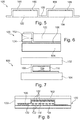
- Figure 4 to Figure 7 illustrate cross-sectional views of electric devices 100 according to other exemplary embodiments of the invention.
- both the first structure 102 and the second structure 104 has a respective sidewall along which a respective portion of the thermo-deformed layer 106 extends.
- the thermo-deformed layer 106 assumes a substantially S-shape to thereby extend along both main surfaces as well as side wall surfaces of the structures 102, 104.
- An extremely compact electric device 100 with highly efficient electric coupling may therefore be obtained. It is also possible that electric signals or electric energy is transported along the S-shape of the correspondingly bent thermo-deformed layer 106.
- first structure 102 and the second structure 104 are arranged side by side, i.e. are located horizontally adjacent to one another. While the various structures 102, 104, 116 have been arranged on top of one another, i.e. have been vertically stacked, in the previously described embodiments, Figure 5 shows an embodiment in which first structure 102 and second structure 104 are electrically connected via the three-dimensionally thermo-deformed layer 106 in a side by side arrangement.
- thermoformed material in combination with the copper on top and/or bottom can also transport heat.
- the first structure 102 has a slit-shaped through hole 124 through which the thermo-deformed layer 106 extends.
- the embodiment of Figure 6 has the advantage of particularly short electric connection paths thanks to the through-hole 124 formed in the first structure 102 in combination with the thermo-deformed layer 106.
- the three-dimensionally bent thermo-deformed layer 106 is guided along exterior surfaces of the first structure 102 and the second structure 104 and extends through the through-hole 124 for providing an extremely short electric connection path.
- thermo-deformed layer 106 is bent in a U-shaped way to contact both opposing main surfaces of the third structure 116.
- the shown electric device 100 allows a simultaneous contacting of pads 168 on both opposing main surfaces of the third structure 116.
- this embodiment has the advantage of a particularly short electric connection path between the first structure 102 and the second structure 104 as well as between the two opposing main surfaces of the third structure 116.
- Figure 8 illustrates a cross-sectional view of an electric device 100 according to another exemplary embodiment of the invention similar to Figure 1 .
Landscapes
- Engineering & Computer Science (AREA)
- Microelectronics & Electronic Packaging (AREA)
- Manufacturing & Machinery (AREA)
- Structure Of Printed Boards (AREA)
- Internal Circuitry In Semiconductor Integrated Circuit Devices (AREA)
- Production Of Multi-Layered Print Wiring Board (AREA)
Abstract
Description
- The invention relates to an electric device and to a method of manufacturing an electric device.
- In the context of growing product functionalities of component carriers equipped with one or more electronic components and increasing miniaturization of such components as well as a rising number of components to be mounted on the component carriers such as printed circuit boards, increasingly more powerful array-like components or packages having several components are being employed, which have a plurality of contacts or connections, with ever smaller spacing between these contacts. In particular, a low loss electric connection of embedded components is desired. For example, component carriers with high I/O count and/or high-frequency signal transmission may be critical in this respect. Moreover, there is a strong tendency in the field of component carriers of continued miniaturization. In particular, it is desired to form electrically conductive connections with smaller and smaller dimensions. Thus, conventional procedures of contacting different layers of stacked layer-type component carriers reach their limits.
- There may be a need to efficiently and compactly establish electric connections in an electric device composed of multiple structures.
- According to an exemplary embodiment of the invention, an electric device is provided which comprises a first structure, a second structure, and a deformed layer comprising a dielectric matrix and electrically conductive elements formed therein, wherein the deformed layer is arranged to electrically couple the first structure with the second structure.
- According to another exemplary embodiment of the invention, a method of manufacturing an electric device it is provided, wherein the method comprises providing a first structure, providing a second structure, and electrically coupling the first structure with the second structure by a deformed layer comprising a dielectric matrix and electrically conductive elements.
- In the context of the present application, the term "electric device" may particularly denote any electric member, module or package in which two or more structures are functionally coupled and electrically connected via a deformed layer with electrically conductive elements therein.
- In the context of the present application, the term "structure" may particularly denote an electric structure such as a physical body providing an electric or electronic functionality. Examples of such a structure are electronic chips, component carriers, electric packages or modules, etc.
- In the context of the present application, the term "deformed layer" may particularly denote a curved, bent or otherwise three-dimensionally deformed layer which is deformed in such a way as to provide a shortened electric connection between structures via electrically conductive elements integrated within the deformed layer. The deformed layer may have a plurality of connected portions, wherein one or more of the portions may extend horizontally and one or more other of the portions may extend vertically.
- According to an exemplary embodiment of the invention, an electric device is provided in which two or more (in particular electric) structures are electrically connected at least partially by a deformed layer having integrated electrically conductive elements. In view of the bent and very thin configuration of the deformed layer, it is possible to electrically connect the structures over a very short spatial distance (which may be for example as small as the thickness of the deformed layer itself). In particular, z-axis coupling of a plate shaped electric device may be accomplished very efficiently in this way. Thus, a highly compact electric device with short current paths can be provided allowing for an efficient and low-loss transport of electric signals and/or electric energy between the structures via the deformed layer. In view of the freely deformable shape of the deformed layer, it is possible for a circuit designer to highly flexibly establish substantially any desired coupling architecture by correspondingly bending the deformed layer.
- With the architecture according to exemplary embodiments of the invention, heavy mechanical drill holes which are not that accurate in alignment and accuracy can be at least partially avoided. Moreover, impedance control of z-axis interconnections may become possible when involving a deformed layer for electrically coupling two structures. The concept of implementing a deformed layer with electrically conductive elements formed therein for electric and mechanical coupling purposes can be considered as a powerful alternative for conventional chip packaging systems. The high flexibility of such an electric device also introduces the possibility of new types of interconnections.
- In the following, further exemplary embodiments of the method and the electric device will be explained.
- In an embodiment, the deformed layer is a thermo-deformed layer or thermally deformed layer (for instance comprising a thermoplastic material). In the context of the present application, the term "thermally deformed" or "thermo-deformed" layer may particularly denote a layer processed by thermoforming. In particular, a thermally deformed layer may be the result of a manufacturing process in which a sheet of an appropriate material (for instance a dielectric (in particular plastic) sheet with embedded electrically conductive elements is heated to a pliable forming temperature, formed to a specific shape in a mold, and trimmed to create a (for instance three-dimensionally) bent thermally deformed layer. The layer, sheet, or film may be heated (for instance in an oven) to a sufficiently high temperature that permits it to be stretched into or onto a form, tool or structure and cooled to a finished shape. When configuring the deformed layer as a thermally deformed layer, it is possible to establish a desired deformation for accomplishing a desired electric connection pattern in a simple way by bringing the layer into a desired deformed configuration and fix the deformed layer in this state by the temporary application of thermal energy. For instance, it is possible to establish such a state by heating a thermally deformable material above a dedicated temperature, for instance a temperature in a range between 150°C and 200°C. The thermo-deformed layer will then maintain its shape permanently after cooling down to ambient temperature and may therefore be capable of precisely serving as a tiny electric connection between two or more structures.
- According to an embodiment of the invention, the material of the deformed layer (in particular a thermoplastic material) comprises at least one of the group consisting of Polyolefins such as Polypropylene (PP), Vinyl-Polymers such as PVC, Styrene based Polymers such as Polystyrene (PS), Polyacrylates such as Polymethylmetaclylate (PMMA), Polyacetals such as Polyoxymetlylene (POM), Fluoropolymers such as Polytetrafluoroethylene (PTFE), Polyamides including aromatic polyamides such as Polyphthalamide (PPA), Polycarbonate (PC) and Derivatives, Polyesters such as Polyethylene terephthalate (PET), Liquid Crystalline Polymers (LCP), Polyarylether such as Polyphenyleneether (PPE), Polyphenylenesulfone (PSU), Polyarylethersulfone (PES), Polyphenylensulfid (PPS), Polyetherketones such as Polyetheretherketone (PEEK), Polyimide (PI), Polyetherimide (PEI), Polyamidimide (PAI).
- In this respect, it is mentioned that in particular the thermoplastic materials PEI, PES, and PSU and LCP may be of advantage because they a capable of withstanding temperatures up to 260°C. This means that these materials can be subjected to a typical reflow soldering process which usually is used in order to form a stable electric connection between the terminals of electronic components being assembled onto the component carrier and connection pads formed on the surface of the component carrier.
- The materials PPE and LCP may be an appropriate choice in particular in case the component carrier is to be used for high frequency applications.
- It has been experimentally proven by the inventors that in particular PEI can be processed in an easy and effective manner when it is existent within a fiber mesh material. This means that a thermoplastic reinforced fiber composite material may be formed which can be used as a prepreg for realizing the described component carrier. However, it is mentioned that also the other described thermoplastic materials can be used in the form of a composite material.
- In an embodiment, at least one of the first structure and the second structure comprises one of the group consisting of a component carrier and a component. Thus, the first and/or the second structure may be substantially any electronic component or component carrier which shall be electrically and mechanically coupled. Therefore, a highly flexible construction set for designing electric devices is provided in which the deformed layer can be adapted for a certain application simply by defining its shape and configuration of its electrically conductive elements.
- In the context of the present application, the term "component carrier" may particularly denote any support structure which is capable of accommodating one or more components thereon and/or therein for providing mechanical support and/or electrical connectivity. In other words, a component carrier may be configured as a mechanical and/or electronic carrier for components. In particular, a component carrier may be one of a rigid or flexible printed circuit board, an organic interposer, and an IC (integrated circuit) substrate. A component carrier may also be a hybrid board combining different ones of the above mentioned-types of component carriers.
- In an embodiment, the component carrier is configured as one of the group consisting of a printed circuit board, and a substrate (in particular an IC substrate). For instance, it is possible to combine two PCBs, to combine two substrates, or to combine one PCB and one substrate for forming an electric device according to an exemplary embodiment of the invention.
- In the context of the present application, the term "printed circuit board" (PCB) may particularly denote a component carrier (which may be plate-shaped (i.e. planar), three-dimensionally curved (for instance when manufactured using 3D printing) or which may have any other shape) which is formed by laminating several electrically conductive layer structures with several electrically insulating layer structures, for instance by applying pressure, if desired accompanied by the supply of thermal energy. As preferred materials for PCB technology, the electrically conductive layer structures are made of copper, whereas the electrically insulating layer structures may comprise resin and/or glass fibers, so-called prepreg or FR4 material. The various electrically conductive layer structures may be connected to one another in a desired way by forming through-holes through the laminate, for instance by laser drilling or mechanical drilling, and by filling them with electrically conductive material (in particular copper), thereby forming vias as through-hole connections. Apart from one or more components which may be embedded in a printed circuit board, a printed circuit board is usually configured for accommodating one or more components on one or both opposing surfaces of the plate-shaped printed circuit board. They may be connected to the respective main surface by soldering. A dielectric part of a PCB may be composed of resin with reinforcing fibers (such as glass fibers).
- In the context of the present application, the term "substrate" may particularly denote a small component carrier having substantially the same size as a component (in particular an electronic component) to be mounted thereon. More specifically, a substrate can be understood as a carrier for electrical connections or electrical networks as well as component carrier comparable to a printed circuit board (PCB), however with a considerably higher density of laterally and/or vertically arranged connections. Lateral connections are for example conductive paths, whereas vertical connections may be for example drill holes. These lateral and/or vertical connections are arranged within the substrate and can be used to provide electrical and/or mechanical connections of housed components or unhoused components (such as bare dies), particularly of IC chips, with a printed circuit board or intermediate printed circuit board. Thus, the term "substrate" also includes "IC substrates". A dielectric part of a substrate may be composed of resin with reinforcing spheres (such as glass spheres).
- The at least one component can be selected from a group consisting of an electrically non-conductive inlay, an electrically conductive inlay (such as a metal inlay, preferably comprising copper or aluminum), a heat transfer unit (for example a heat pipe), a light guiding element (for example an optical waveguide or a light conductor connection), an electronic component, or combinations thereof. For example, the component can be an active electronic component, a passive electronic component, an electronic chip, a storage device (for instance a DRAM or another data memory), a filter, an integrated circuit, a signal processing component, a power management component, an optoelectronic interface element, a voltage converter (for example a DC/DC converter or an AC/DC converter), a cryptographic component, a transmitter and/or receiver, an electromechanical transducer, a sensor, an actuator, a microelectromechanical system (MEMS), a microprocessor, a capacitor, a resistor, an inductance, a battery, a switch, a camera, an antenna, a logic chip, a light guide, and an energy harvesting unit. However, other components may be used as well. For example, a magnetic element can be used as a component. Such a magnetic element may be a permanent magnetic element (such as a ferromagnetic element, an antiferromagnetic element or a ferrimagnetic element, for instance a ferrite base structure) or may be a paramagnetic element. However, the component may also be a further component carrier, for example in a board-in-board configuration. One or more components may be surface mounted and/or may be embedded in an interior of the electric device.
- For example, the respective component carrier may be a stack or laminate of electrically insulating layer structure(s) and electrically conductive layer structure(s), in particular formed by applying mechanical pressure, if desired supported by thermal energy. The mentioned stack may provide a plate-shaped component carrier capable of providing a large mounting surface for further components and being nevertheless very thin and compact.
- In particular, the stack of layer structures may be connected with one another by lamination, i.e. the application of thermal energy and/or heat. In other words, the stack may be a laminate.
- In the context of the present application, the term "layer structure" may particularly denote a continuous layer, a patterned layer or a plurality of nonconsecutive islands within a common plane. In the context of the present application, the term "stack" may particularly denote an arrangement of multiple planar layer structures which are mounted in parallel on top of one another.
- In an embodiment, the component carrier as well as the electric device is shaped as a plate. This contributes to the compact design, wherein the component carrier(s) nevertheless provide(s) a large basis for mounting components thereon. Furthermore, in particular a naked die as example for an embedded electronic component, can be conveniently embedded, thanks to its small thickness, into a thin plate such as a printed circuit board.
- In an embodiment, the electrically insulating layer structures comprises at least one of the group consisting of resin (such as reinforced or non-reinforced resins, for instance epoxy resin or Bismaleimide-Triazine resin, more specifically FR-4, FR-5 or ABF®), cyanate ester, polyphenylene derivate, glass (in particular glass fibers, multi-layer glass, glass-like materials), prepreg material, polyimide, polyamide, liquid crystal polymer (LCP), epoxy-based Build-Up Film, polytetrafluoroethylene (Teflon), a ceramic, and a metal oxide. Reinforcing materials such as webs, fibers or spheres, for example made of glass (multilayer glass) may be used as well. Although prepreg or FR4 are usually preferred, other materials may be used as well. For high frequency applications, high-frequency materials such as polytetrafluoroethylene, liquid crystal polymer and/or cyanate ester resins may be implemented in the component carrier as electrically insulating layer structure.
- In an embodiment, the electrically conductive layer structures comprise at least one of the group consisting of copper, aluminum, nickel, silver, gold, palladium, and tungsten. Although copper is usually preferred, other materials or coated versions thereof are possible as well, in particular coated with supra-conductive material such as graphene.
- In an embodiment, the dielectric matrix comprises at least one of the group consisting of polyimide, polyamide, and liquid crystal polymer. These materials and other flexible materials are capable of being thermo-deformable. In other words, it is possible to bring a layer made of one of the mentioned materials into a three-dimensional bending state and freeze the latter into this three-dimensional configuration by the application of heat. Highly advantageously, the mentioned materials are compatible with component carrier technology, in particular printed circuit board technology and may therefore be properly integrated into the electric device.
- In an embodiment, the deformed layer extends in bent shape along at least one of the first structure and the second structure. In particular, different portions of the deformed layer may extend in parallel to a respective surface of a for instance plate-shaped or cuboid-shaped structure. By such a configuration, it is possible to very closely locate the structures to be coupled, for instance separated only by the thin deformed layer. It is also possible by such a bending architecture to functionalize the deformed layer in such a way that even a mechanical accommodation space may be defined in accordance with the specific shape and/or dimension of a respective one of the structures. For instance, a cavity may be defined by the three-dimensionally bent configuration of the deformed layer which fits to a shape and dimension of a respective one of the structures.
- In an embodiment, the electric device comprises a third structure electrically coupled with at least one of the first structure and the second structure by the deformed layer. According to such a preferred embodiment, a third structure is added which is electrically coupled between the first structure and the second structure. Therefore, a package or module type electric device may be formed which has very short electric connection paths between the third structure and the first and/or second structure.
- In an embodiment, the third structure comprises or consists of an electronic chip, in particular a semiconductor chip. For example, the third structure may be a semiconductor chip such as a processor or a memory. However, the third structure may be also any other kind of component carrier or component. Reference is made to the examples given above for the first and the second structure. All embodiments described herein for the first and second structure may also apply to the third structure. All embodiments described herein for the third structure may also apply to the first and second structure. It is also possible that the third structure is a component carrier such as a printed circuit board or an IC substrate, an interposer or the like. This large list of possible embodiments of the third structure shows the high flexibility involved by the concept according to an exemplary embodiment of the invention.
- In an embodiment, the deformed layer is bent to form a cavity in which the third structure is inserted. In particular, the shape of the cavity may match to the shape of the third structure so that a form closure may be obtained when placing the third structure in the cavity. Such a cavity may define a specifically adapted accommodation volume for a respective one of the first, second and/or third structures and may have a support surface for supporting a main surface of the respective structure, as well as sidewalls for delimiting a lateral spatial dimension of the respective structure.
- In an embodiment, the deformed layer is bent to contact both opposing main surfaces of the third structure. According to such a configuration, a complex bending architecture may be involved which allows to electrically contact both opposing main surfaces of the third (and/or the first and/or the second) structure via a single deformed layer. For instance, this may be accomplished by configuring the deformed layer or at least a portion thereof to assume a substantially U-shape for enabling the described coupling architecture.
- In an embodiment, the electric device comprises an encapsulating medium at least partially encapsulating at least one of the group consisting of the deformed layer, the first structure, the second structure, and the third structure. By such an encapsulating medium, the configuration of the various structures to be interconnected may be fixed in place. At the same time, such an encapsulating medium may provide a mechanical protection of sensitive structures such as electronic chips. In one embodiment, the mentioned encapsulating medium may embed the third structure as well as at least a portion of the deformed layer while the first and second structure may remain externally exposed with regard to the encapsulation medium for electric contacting processes.
- In an embodiment, the encapsulating medium is a mold medium. Such a mold medium may be for instance a viscous plastic which may be filled in a mold tool and may be cured by the application of thermal energy and/or pressure so that the mold medium solidifies and provides a mechanical protection shell as well as a dielectric decoupling structure preventing undesired electric paths in an interior of the electric device.
- In an embodiment, the electric device comprises vertical interconnect structures, in particular vias, providing an electric connection between a respective one of the first structure and the second structure on the one hand and the deformed layer on the other hand. In order to provide for an access into an interior of the above described encapsulation medium, for example, the mentioned vias may be formed by laser processing or mechanically drilling. Subsequently, the so manufactured vias may be filled with electrically conductive material such as copper. Therefore, the electric coupling performance provided by the deformed layer may be accompanied by an additional electric wiring structure provided by the metal filed vias. Preferably, such vias extend from an exterior through a part of the encapsulation medium to thereby contribute to the electric connection paths between the first and/or second structure (extending beyond the encapsulation medium) on the one hand and the third structure and/or the deformed layer (which may be partially or completely within the encapsulation medium) on the other hand.
- In an embodiment, the electric device comprises vertical interconnect structures, in particular vias, contributing to an electric connection between at least one of the first structure and the second structure on the one hand and the third structure on the other hand. In particular, it is possible that the complete electric path from the third structure to the first or second structure is composed of the electrically conductive elements in combination with the vertical interconnect structures. It is however also possible that the complete electric path from the third structure to the first or second structure is provided by the vertical interconnect structures alone. In yet another alternative, it is possible that the complete electric path from the third structure to the first or second structure is provided by the electrically conductive elements alone.
- In an embodiment, at least one of the first structure and the second structure has a main surface along which at least part of the deformed layer extends. For instance, such a main surface may include electrically conductive connection elements of the respective first and/or second structure. Such electrically conductive connection elements may for instance be pads of a semiconductor chip or traces or pads of a component carrier such as a PCB, an IC substrate or an interposer. It should be mentioned that, additionally or alternatively to the mentioned vias, the vertical interconnect structures may also be embodied as metallic pillars, for instance copper pillars. Also such pillars may be integrated in an encapsulating medium.
- In an embodiment, at least one of the first structure and the second structure has a sidewall along which at least part of the deformed layer extends. According to such an embodiment, it is also possible to electrically, thermally and/or mechanically contact sidewalls of a structure (such as a component). Guiding the deformed layer along the sidewall may in particular fulfil an electric connection purpose. Additionally or alternatively, it is however also possible that a portion of the deformed layer extending along a sidewall of the respective structure may contribute to a cooling function, for instance when a portion of the deformed layer extending along such a sidewall is made of a highly thermally conductive material such as copper. It is also possible to use a portion of the deformed layer extending along a sidewall for electromagnetic shielding purposes. In other words, the respective portion of the deformed layer may be made of an appropriate material (for instance a magnetic material) configured for preventing propagation of electromagnetic radiation between an interior and an exterior of the electric device. Such high frequency electromagnetic radiation may deteriorate functionality of components of an electronic environment. By taking the mentioned measure, it is also possible to establish an efficient electromagnetic shielding very close to the respective structure. Additionally, it should be said that it is also possible to provide the mentioned cooling and/or electromagnetic shielding and/or any further functional effect by portions of the deformed layer extending along a main surface of the respective structure.
- In an embodiment, at least one of the first structure and the second structure has a through hole (such as a slit) through which the deformed layer extends. By configuring a respective one of the structures with a slit or the like, it is possible to guide the flexibly bendable deformed structure through the slit, recess or other kind of through-hole so as to establish a very short electric connection path between opposing main surfaces of the respective structure.
- In an embodiment, the deformed layer is present in a defined permanently bent state in which the deformed layer is still elastically bendable. In particular, the dielectric matrix of the deformed layer may be configured so that an elastic property is maintained even after having fixed the general shape of the deformed layer, in particular thermally. This allows the deformed layer to adapt its shape concerning tolerances, temperature changes or other phenomena in the electric device without exerting excessive mechanical load to the constituents of the electric device.
- In an embodiment, the electrically conductive elements form a redistribution structure. Such a redistribution structure, in particular redistribution layer, may comprise electrically conductive elements in the deformed layer which are configured to translate between relatively small dimensions of structures of one technology (such as pad dimensions and/or distances of a semiconductor component) and larger dimensions of structures of a second technology (such as dimensions of the component carrier world, such as the dimension of pads and traces of a PCB). In other words, an electric fan-out function may be provided by a redistribution structure integrated into the deformed layer.
- In an embodiment, the first structure and the second structure are arranged above each another. Therefore, the described packaging architecture may vertically stack the structures.
- In another embodiment, the first structure and the second structure are arranged side by side. Hence, it is also possible to arrange the structures to be electrically coupled juxtaposed or adjacent to one another, i.e. so that sidewalls of the respective structures face each other.
- In an embodiment, the electrically conductive elements of the deformed layer form an impedance controlled electric connection circuitry. Thus, an impedance controlled electric connection circuitry may be provided with the mentioned configuration. Impedance may be denoted as the sum of the resistance and reactance (composed, in turn, of capacitance and inductance) of an electrical circuit. In particular in high speed AC circuits specifically the reactance can become significant. According to the described embodiment, an impedance control may be implemented by the deformed layer sandwiched between the structures. For instance, one of the electrically conductive elements of the deformed layer may be at electric ground potential, whereas an electric signal may be guided along another one of the electrically conductive elements of the deformed layer. As a result, an impedance controlled electric connection circuitry may be obtained.
- In an embodiment, the method comprises thermo-deforming a thermal-deformable layer for forming the deformed layer to thereby accomplish the electric coupling. However, it is also possible to deform the layer by another or an additional impact, for instance the application of pressure.
- In an embodiment, the method comprises electrically coupling the first structure with the second structure by the deformed layer by at least one of the group consisting of thermal compression bonding, directly pressing, and laser via connection. However, other connection techniques may be applied as well.
- The aspects defined above and further aspects of the invention are apparent from the examples of embodiment to be described hereinafter and are explained with reference to these examples of embodiment.
-
Figure 1 illustrates a cross-sectional view of an electric device according to an exemplary embodiment of the invention. -
Figure 2 is a cross-sectional view of constituents of the electric device ofFigure 1 . -
Figure 3 is a plan view of constituents of the electric device ofFigure 1 and Figure 2 . -
Figure 4 to Figure 7 illustrate cross-sectional views of electric devices according to other exemplary embodiments of the invention. -
Figure 8 illustrates a cross-sectional view of an electric device according to another exemplary embodiment of the invention similar toFigure 1 . - The illustrations in the drawings are schematic. In different drawings, similar or identical elements are provided with the same reference signs.
- Before, referring to the drawings, exemplary embodiments will be described in further detail, some basic considerations will be summarized based on which exemplary embodiments of the invention have been developed.
- According to an exemplary embodiment of the invention, an electric device is provided which electrically couples different structures via a deformed layer with electrically conductive elements therein. In particular, such an electric device can be configured as a multi component package with flexible thermoformed interconnect structures in form of the deformed layer.
- Generally, z-axis interconnection is a process in component carrier technology which requires high accuracy alignment, as well as drill machines and precise drillers which may involve high effort and complexity. Beside this, via holes which may be conventionally used for the purpose of z-axis interconnecting do not have precisely defined impedance which can cause drawbacks in high speed transmission lines.
- A z-axis interconnection with traces instead, as provided by exemplary embodiments of the invention in form of a (in particular thermo-) deformed layer with electrically conductive elements formed therein, may help to improve electric performance of a correspondingly manufactured electric device or package.
- Additionally or alternatively to the use of metal plated drill holes, thermoformed flexible PCBs - as an example for the mentioned deformed layer - can be used to realize the interconnection between two or more different structures. The connection between a corresponding one of these structures and the deformed layer (in particular a thermoformed flex-PCB) can be achieved advantageously for instance by thermocompression bonding, i.e. by directly pressing with the structure, or by a laser via connection.
- Conventionally, drilling is the most common way to achieve z-axis interconnections. In most cases the impedance jumps cause electrical problems.
- According to exemplary embodiments of the invention, heavy mechanical drill holes, which are in many cases not that accurate in alignment and accuracy, can be largely avoided. Moreover, exemplary embodiments of the invention render impedance control of z-axis interconnections possible. Furthermore, exemplary embodiments of the invention may be implemented in substantially every build-up where different structures have to be connected in z-axis direction. Descriptively speaking, exemplary embodiments of the invention replace mechanical connections by thermoformed flexible PCBs which are implemented (for instance embedded) into a preferably rigid PCB.
-
Figure 1 illustrates a cross-sectional view of anelectric device 100 according to an exemplary embodiment of the invention.Figure 2 is a cross-sectional view of constituents of theelectric device 100 ofFigure 1. Figure 3 is a plan view of constituents of theelectric device 100 ofFigure 1 and Figure 2 . - The
electric device 100 comprises afirst structure 102 which may be for instance a planar laminar type rigid component carrier such as a printed circuit board, PCB. Furthermore, theelectric device 100 comprises asecond structure 104 which may be for instance another planar laminar type rigid component carrier such as another PCB. Thefirst structure 102 and thesecond structure 104 are vertically stacked. As can be taken from adetail 160 inFigure 1 , the component carrier forming thefirst structure 102 comprises a laminated stack composed of electrically conductive layer structures 112 (in particular copper vias and patterned and/or continuous copper foils) and electrically insulating layer structures 114 (which may comprise resin such as epoxy resin, optionally additionally comprising reinforcing particles such as glass fibers, more specifically prepreg or FR4). The other component carrier forming thesecond structure 104 may also comprise a laminated stack composed of electricallyconductive layer structures 112 and electrically insulatinglayer structures 114. - A thermo-deformed
layer 106 with a stepped shape is provided for accomplishing a vertical electric interconnection between thefirst structure 102 and thesecond structure 104. The thermo-deformedlayer 106 is present in a defined permanently bent state in which the thermo-deformedlayer 106 may be still elastically bendable. The thermo-deformedlayer 106 may be interconnected between thefirst structure 102 and thesecond structure 104, preferably by thermocompression. The thermo-deformedlayer 106 comprises a flexible dielectric matrix 108 (for example made of polyimide) and electrically conductive elements 110 (which may be made of copper) formed therein (comparedetail 162 shown inFigure 2 ). The electricallyconductive elements 110 may form a redistribution structure. The thermo-deformedlayer 106 is vertically sandwiched between thefirst structure 102 and thesecond structure 104 and is spaced with regard to thefirst structure 102 and thesecond structure 104 also via respectivevertical interconnect structures 122. Hence, the electricallyconductive elements 110 in combination with thevertical interconnect structures 122 electrically couple thefirst structure 102 with thesecond structure 104. The thermo-deformedlayer 106 extends in bent shape along thefirst structure 102 and thesecond structure 104. - Moreover, a third structure 116 (such as a semiconductor chip) is electrically coupled with both the
first structure 102 and thesecond structure 104 by the electricallyconductive elements 110 of the thermo-deformedlayer 106 and by thevertical interconnect structures 122. Apart from this electric coupling task, the thermo-deformedlayer 106 is bent to form acavity 118 in which thethird structure 116 matches and is inserted. - Beyond this, the
electric device 100 comprises a mold-type encapsulating medium 120 which encapsulates the thermo-deformedlayer 106 and thethird structure 116 and in which thevertical interconnect structures 122 are formed. Thefirst structure 102 and thesecond structure 104 are also in direct physical contact with the encapsulatingmedium 120. - According to
Figure 1 , the thermo-deformedlayer 106 may have a stepped configuration to thereby definecavity 118 as an accommodation volume of thethird structure 116. In other words, the thermo-deformedlayer 106 extends not only along a main surface of the plate-shapedthird structure 116, but also laterally confines thethird structure 116 by extending along the sidewalls of thethird structure 116. At the same time, the illustrated shape of the thermo-deformedlayer 106 ensures a vertically highly compact configuration of theelectric device 100 and short connection paths in the vertical or z-direction. Theelectric device 100 is hence a flat module or package. - In the shown embodiment, the
third structure 116 may for instance be a semiconductor chip having pads (not shown) both on an upper and a lower main surface thereof. The pads on the lower main surface are contacted with thesecond structure 104 via thevertical interconnect structures 122 which are here embodied as copper filled laser vias extending through the moldtype encapsulating medium 120. The pads on the upper main surface of thethird structure 116 are electrically coupled with the electricallyconductive elements 110 within the thermo-deformedlayer 106. The latter mentioned electricallyconductive elements 110 of the thermo-deformedlayer 106 are further connected via electrically conductive vertical through-connections 122 with thefirst structure 102. - As can be taken from the
detail 160 inFigure 1 , thefirst structure 102 is configured as a printed circuit board, i.e. a component carrier comprising an interconnected stack of electrically conductive layer structures 112 (such as copper foils and copper vias) as well as electrically insulating layer structures 114 (such as prepreg or FR4 layers). The electrically insulatinglayer structures 114 may be, more generally, resin layers (for instance made of epoxy resin) which may optionally have reinforcing particles (such as glass fibres or glass spheres) therein. Thesecond structure 104 may for instance be also a PCB or other component carrier, as thefirst structure 102. It is however also possible that the first and/or thesecond structure - As can be taken from
Figure 1 , a highly compact and highly efficient electric connection architecture with very short electric connection paths in particular in the vertical direction according toFigure 1 is obtained. - The cross-sectional view of
Figure 2 shows in particular the internal composition of the thermo-deformedlayer 106. The latter can be taken fromdetail 162 ofFigure 2 . As shown, the thermo-deformedlayer 106 may comprise one or more dielectric layers forming thedielectric matrix 108 made of an elastic and thermally deformable material such as polyimide. Within this one or more dielectric layers, the electricallyconductive elements 110 are embedded, for instance copper structures. In the shown embodiment, electricallyconductive elements 110 in differentdielectric layers 108 have different dimensions, so that the arrangement shown indetail 162 functions as a redistribution layer (RDL) translating between the small pad dimensions of the semiconductor world and the larger electric dimensions of the PCB world. - By the three-dimensional bending of the thermo-deformed
layer 106 according toFigure 2 , thecavity 118 for accommodating thethird structure 116 is formed, thereby providing a mechanical guiding function in addition to the electric coupling function. -
Figure 3 shows a plan view of the architecture illustrated inFigure 2 . Bendinglines 164 inFigure 3 illustrate positions where the thermo-deformedlayer 106 may be bent in order to define thecavity 118 and in order to provide the electric coupling functionality described above.Figure 3 moreover shows electricallyconductive connection paths 166 within the thermo-deformedlayer 106 which may be formed by the electricallyconductive elements 110. -
Figure 4 to Figure 7 illustrate cross-sectional views ofelectric devices 100 according to other exemplary embodiments of the invention. - Referring to
Figure 4 , both thefirst structure 102 and thesecond structure 104 has a respective sidewall along which a respective portion of the thermo-deformedlayer 106 extends. In the embodiment shown inFigure 4 , the thermo-deformedlayer 106 assumes a substantially S-shape to thereby extend along both main surfaces as well as side wall surfaces of thestructures electric device 100 with highly efficient electric coupling may therefore be obtained. It is also possible that electric signals or electric energy is transported along the S-shape of the correspondingly bent thermo-deformedlayer 106. - Referring to
Figure 5 , thefirst structure 102 and thesecond structure 104 are arranged side by side, i.e. are located horizontally adjacent to one another. While thevarious structures Figure 5 shows an embodiment in whichfirst structure 102 andsecond structure 104 are electrically connected via the three-dimensionally thermo-deformedlayer 106 in a side by side arrangement. - In embodiments, the thermoformed material in combination with the copper on top and/or bottom can also transport heat.
- Referring to
Figure 6 , thefirst structure 102 has a slit-shaped throughhole 124 through which the thermo-deformedlayer 106 extends. The embodiment ofFigure 6 has the advantage of particularly short electric connection paths thanks to the through-hole 124 formed in thefirst structure 102 in combination with the thermo-deformedlayer 106. The three-dimensionally bent thermo-deformedlayer 106 is guided along exterior surfaces of thefirst structure 102 and thesecond structure 104 and extends through the through-hole 124 for providing an extremely short electric connection path. - Referring to
Figure 7 , the thermo-deformedlayer 106 is bent in a U-shaped way to contact both opposing main surfaces of thethird structure 116. With the U-shaped configuration according toFigure 7 , the shownelectric device 100 allows a simultaneous contacting ofpads 168 on both opposing main surfaces of thethird structure 116. Also this embodiment has the advantage of a particularly short electric connection path between thefirst structure 102 and thesecond structure 104 as well as between the two opposing main surfaces of thethird structure 116. -
Figure 8 illustrates a cross-sectional view of anelectric device 100 according to another exemplary embodiment of the invention similar toFigure 1 . - It should be noted that the term "comprising" does not exclude other elements or steps and the "a" or "an" does not exclude a plurality. Also elements described in association with different embodiments may be combined.
- It should also be noted that reference signs in the claims shall not be construed as limiting the scope of the claims.
- Implementation of the invention is not limited to the preferred embodiments shown in the figures and described above. Instead, a multiplicity of variants are possible which use the solutions shown and the principle according to the invention even in the case of fundamentally different embodiments.
Claims (14)
- An electric device, comprising:a first structure;a second structure,a deformed layer comprising a dielectric matrix and electrically conductive elements formed therein;wherein the deformed layer is arranged to electrically couple the first structure with the second structure.
- The electric device according to claim 1, wherein at least one of the first structure and the second structure comprises one of the group consisting of a component carrier and a component.
- The electric device according to claim 2, comprising at least one of the following features:the component carrier is shaped as a plate;the component carrier is configured as a printed circuit board or a substrate;the component comprises at least one of the group consisting of an electronic component, an electrically non-conductive and/or electrically conductive inlay, a heat transfer unit, an energy harvesting unit, an active electronic component, a passive electronic component, an electronic chip, a package, a storage device, a filter, an integrated circuit, a signal processing component, a power management component, an optoelectronic interface element, a voltage converter, a cryptographic component, a transmitter and/or receiver, an electromechanical transducer, an actuator, a microelectromechanical system, a microprocessor, a capacitor, a resistor, an inductance, an accumulator, a switch, a camera, an antenna, a magnetic element, a light guiding element, a further component carrier and a logic chip.
- The electric device according to claim 2, wherein the component carrier comprises a stack comprising at least one electrically conductive layer structure and at least one electrically insulating layer structure.
- The electric device according to claim 4, comprising at least one of the following features:the at least one electrically conductive layer structure comprises at least one of the group consisting of copper, aluminum, nickel, silver, gold, palladium, and tungsten, any of the mentioned materials being optionally coated with supra-conductive material such as graphene;the at least one electrically insulating layer structure comprises at least one of the group consisting of resin, in particular reinforced or non-reinforced resin, for instance epoxy resin or Bismaleimide-Triazine resin, FR-4, FR-5, cyanate ester, polyphenylene derivate, glass, prepreg material, polyimide, polyamide, liquid crystal polymer, epoxy-based Build-Up Film, polytetrafluoroethylene, a ceramic, and a metal oxide.
- The electric device according to claim 1, comprising at least one of the following features:the deformed layer is a thermo-deformed layer;the dielectric matrix comprises at least one of the group consisting of polyimide, polyamide, and liquid crystal polymer;the deformed layer extends in bent shape along at least part of at least one of the first structure and the second structure;the electric device comprises vertical interconnect structures, in particular vias, providing an electric connection between a respective one of the first structure and the second structure on the one hand and the deformed layer on the other hand.
- The electric device according to claim 1, wherein the electric device comprises a third structure electrically coupled with at least one of the first structure and the second structure by the deformed layer.
- The electric device according to claim 7, comprising at least one of the following features:the third structure comprises or consists of an electronic chip, in particular a semiconductor chip;the deformed layer is bent to form a cavity in which the third structure is inserted;the deformed layer is bent to contact both opposing main surfaces of the third structure;the electric device comprises vertical interconnect structures, in particular vias, contributing to an electric connection between at least one of the first structure and the second structure on the one hand and the third structure on the other hand.
- The electric device according to claim 1, wherein the electric device comprises an encapsulating medium at least partially encapsulating at least part of at least one of the group consisting of the deformed layer, the first structure, and the second structure.
- The electric device according to claim 9, wherein the encapsulating medium is a mold medium.
- The electric device according to claim 1, comprising at least one of the following features:wherein at least one of the first structure and the second structure has a main surface along which at least part of the deformed layer extends;wherein at least one of the first structure and the second structure has a sidewall along which at least part of the deformed layer extends;wherein at least one of the first structure and the second structure has a through hole through which the deformed layer extends;wherein the deformed layer is present in a defined permanently bent state in which the deformed layer is still elastically bendable;wherein the electrically conductive elements form a redistribution structure;wherein the first structure and the second structure are arranged above each another;wherein the first structure and the second structure are arranged side by side;wherein the electrically conductive elements of the deformed layer form an impedance controlled electric connection circuitry;wherein the dielectric matrix of the deformed layer comprises at least one of the group consisting of a thermoplastic material, Polyolefins such as Polypropylene, Vinyl-Polymers, Styrene based Polymers such as Polystyrene, Polyacrylates such as Polymethylmetaclylate, Polyacetals such as Polyoxymetlylene, Fluoropolymers such as Polytetrafluoroethylene, Polyamides including aromatic polyamides such as Polyphthalamide, Polycarbonate and Derivatives, Polyesters such as Polyethylene terephthalate, Liquid Crystalline Polymers, Polyarylether such as Polyphenyleneether, Polyphenylenesulfone, Polyarylethersulfone, Polyphenylensulfid, Polyetherketones such as Polyetheretherketone, Polyimide, Polyetherimide, and Polyamidimide.
- A method of manufacturing an electric device, wherein the method comprises:providing a first structure;providing a second structure;electrically coupling the first structure with the second structure by a deformed layer comprising a dielectric matrix and electrically conductive elements.
- The method according to claim 12, wherein the method comprises thermo-deforming a thermal-deformable layer for forming the deformed layer to thereby accomplish the electric coupling.
- The method according to claim 13, wherein the method comprises electrically coupling the first structure with the second structure by the deformed layer by at least one of the group consisting of thermal compression bonding, directly pressing, and laser via connection.
Priority Applications (1)
| Application Number | Priority Date | Filing Date | Title |
|---|---|---|---|
| EP25187126.5A EP4608077A3 (en) | 2018-06-07 | 2019-06-06 | Deformed layer for short electric connection between structures of electric device |
Applications Claiming Priority (1)
| Application Number | Priority Date | Filing Date | Title |
|---|---|---|---|
| US16/002,202 US10410963B1 (en) | 2018-06-07 | 2018-06-07 | Deformed layer for short electric connection between structures of electric device |
Related Child Applications (1)
| Application Number | Title | Priority Date | Filing Date |
|---|---|---|---|
| EP25187126.5A Division EP4608077A3 (en) | 2018-06-07 | 2019-06-06 | Deformed layer for short electric connection between structures of electric device |
Publications (2)
| Publication Number | Publication Date |
|---|---|
| EP3579669A2 true EP3579669A2 (en) | 2019-12-11 |
| EP3579669A3 EP3579669A3 (en) | 2020-04-29 |
Family
ID=66810682
Family Applications (2)
| Application Number | Title | Priority Date | Filing Date |
|---|---|---|---|
| EP25187126.5A Pending EP4608077A3 (en) | 2018-06-07 | 2019-06-06 | Deformed layer for short electric connection between structures of electric device |
| EP19178671.4A Pending EP3579669A3 (en) | 2018-06-07 | 2019-06-06 | Deformed layer for short electric connection between structures of electric device |
Family Applications Before (1)
| Application Number | Title | Priority Date | Filing Date |
|---|---|---|---|
| EP25187126.5A Pending EP4608077A3 (en) | 2018-06-07 | 2019-06-06 | Deformed layer for short electric connection between structures of electric device |
Country Status (3)
| Country | Link |
|---|---|
| US (1) | US10410963B1 (en) |
| EP (2) | EP4608077A3 (en) |
| CN (1) | CN110581417B (en) |
Families Citing this family (6)
| Publication number | Priority date | Publication date | Assignee | Title |
|---|---|---|---|---|
| EP3439438B1 (en) * | 2017-08-02 | 2024-10-09 | AT & S Austria Technologie & Systemtechnik Aktiengesellschaft | Non-uniform magnetic foil embedded in component carrier |
| US10840197B2 (en) * | 2018-10-30 | 2020-11-17 | Taiwan Semiconductor Manufacturing Company, Ltd. | Package structure and manufacturing method thereof |
| US12245377B2 (en) * | 2019-03-29 | 2025-03-04 | At&S Austria Technologie & Systemtechnik Aktiengesellschaft | Component carrier with embedded semiconductor component and embedded highly-conductive block which are mutually coupled |
| EP3840542A1 (en) * | 2019-12-18 | 2021-06-23 | AT & S Austria Technologie & Systemtechnik Aktiengesellschaft | Compact laminated component carrier with front end chip and impedance matching circuitry for antenna communication |
| CN110932530A (en) * | 2020-01-16 | 2020-03-27 | 联振电子(深圳)有限公司 | Novel coupling inductance suitable for 3D type power module |
| IL274946B2 (en) * | 2020-05-26 | 2026-05-01 | Elta Systems Ltd | Encapsulation techniques |
Citations (5)
| Publication number | Priority date | Publication date | Assignee | Title |
|---|---|---|---|---|
| US20040150107A1 (en) * | 2002-12-31 | 2004-08-05 | Cha Ki Bon | Stack package and fabricating method thereof |
| EP2288242A1 (en) * | 2009-07-31 | 2011-02-23 | Raytheon Company | Multi-layer microwave corrugated printed circuit board and method |
| GB2482039A (en) * | 2010-07-16 | 2012-01-18 | Novalia Ltd | A laminate electronic device |
| US20140021624A1 (en) * | 2012-07-17 | 2014-01-23 | Olympus Corporation | Mounting structure of semiconductor device and method of manufacturing the same |
| US20160315044A1 (en) * | 2014-12-16 | 2016-10-27 | Industrial Technology Research Institute | Electronic device package, electronic device structure and method of fabricating electronic device package |
Family Cites Families (16)
| Publication number | Priority date | Publication date | Assignee | Title |
|---|---|---|---|---|
| JP2000068444A (en) | 1998-08-26 | 2000-03-03 | Mitsubishi Electric Corp | Semiconductor device |
| JP2004179300A (en) | 2002-11-26 | 2004-06-24 | Renesas Technology Corp | Semiconductor device and method of manufacturing the same |
| JP4842761B2 (en) * | 2006-03-28 | 2011-12-21 | 日本碍子株式会社 | Electrical connection body and manufacturing method thereof |
| TWI307946B (en) * | 2006-05-24 | 2009-03-21 | Phoenix Prec Technology Corp | Stack structure of circuit board having embedded with semicondutor component |
| WO2009090879A1 (en) * | 2008-01-18 | 2009-07-23 | Panasonic Corporation | Three-dimensional wiring board |
| JP2011243897A (en) | 2010-05-21 | 2011-12-01 | Fujitsu Ltd | Multilayer printed board and method of manufacturing the same |
| TW201244598A (en) * | 2011-04-22 | 2012-11-01 | Walton Advanced Eng Inc | Thin carrier device |
| US8664540B2 (en) * | 2011-05-27 | 2014-03-04 | Taiwan Semiconductor Manufacturing Company, Ltd. | Interposer testing using dummy connections |
| US20130069218A1 (en) | 2011-09-20 | 2013-03-21 | Stmicroelectronics Asia Pacific Pte Ltd. | High density package interconnect with copper heat spreader and method of making the same |
| WO2013052347A1 (en) * | 2011-10-03 | 2013-04-11 | Invensas Corporation | Memory module in a package and its pin configuration |
| CN205093042U (en) * | 2013-05-13 | 2016-03-16 | 株式会社村田制作所 | flexible circuit substrate |
| JP6641085B2 (en) * | 2015-01-16 | 2020-02-05 | 日立金属株式会社 | Repeater |
| KR20170034957A (en) | 2015-09-21 | 2017-03-30 | 에스케이하이닉스 주식회사 | Semiconductor package including flexible wing interconnection substrate |
| CN107871732A (en) * | 2016-09-23 | 2018-04-03 | 深圳市中兴微电子技术有限公司 | Encapsulating structure |
| CN207022286U (en) * | 2017-01-13 | 2018-02-16 | 奥特斯(中国)有限公司 | For manufacturing the semi-finished product and its part bearing part of part bearing part |
| CN108364872B (en) * | 2017-01-26 | 2020-08-18 | 光宝电子(广州)有限公司 | Electronic product and method of manufacturing the same |
-
2018
- 2018-06-07 US US16/002,202 patent/US10410963B1/en active Active
-
2019
- 2019-06-06 EP EP25187126.5A patent/EP4608077A3/en active Pending
- 2019-06-06 EP EP19178671.4A patent/EP3579669A3/en active Pending
- 2019-06-06 CN CN201910491674.9A patent/CN110581417B/en active Active
Patent Citations (5)
| Publication number | Priority date | Publication date | Assignee | Title |
|---|---|---|---|---|
| US20040150107A1 (en) * | 2002-12-31 | 2004-08-05 | Cha Ki Bon | Stack package and fabricating method thereof |
| EP2288242A1 (en) * | 2009-07-31 | 2011-02-23 | Raytheon Company | Multi-layer microwave corrugated printed circuit board and method |
| GB2482039A (en) * | 2010-07-16 | 2012-01-18 | Novalia Ltd | A laminate electronic device |
| US20140021624A1 (en) * | 2012-07-17 | 2014-01-23 | Olympus Corporation | Mounting structure of semiconductor device and method of manufacturing the same |
| US20160315044A1 (en) * | 2014-12-16 | 2016-10-27 | Industrial Technology Research Institute | Electronic device package, electronic device structure and method of fabricating electronic device package |
Also Published As
| Publication number | Publication date |
|---|---|
| EP3579669A3 (en) | 2020-04-29 |
| EP4608077A2 (en) | 2025-08-27 |
| EP4608077A3 (en) | 2025-11-19 |
| US10410963B1 (en) | 2019-09-10 |
| CN110581417A (en) | 2019-12-17 |
| CN110581417B (en) | 2022-09-30 |
Similar Documents
| Publication | Publication Date | Title |
|---|---|---|
| EP3547361B1 (en) | Component carrier connected with tilted other component carrier for short electric connection | |
| US10410963B1 (en) | Deformed layer for short electric connection between structures of electric device | |
| US11810844B2 (en) | Component carrier and method of manufacturing the same | |
| US11051391B2 (en) | Thermally highly conductive coating on base structure accommodating a component | |
| US11574849B2 (en) | Package with embedded electronic component being encapsulated in a pressureless way | |
| US10595414B2 (en) | Component carrier and manufacturing method | |
| US11129314B2 (en) | Stepped component assembly accommodated within a stepped cavity in component carrier | |
| US10887977B2 (en) | Hybrid component carrier and method for manufacturing the same | |
| US20190174638A1 (en) | Cooling Component Carrier Material by Carbon Structure Within Dielectric Shell | |
| EP3340753B1 (en) | Method of integrating a connector member with component carrier | |
| EP3349247B1 (en) | Patterned cover layer on base structure defining cavity and alignment marker | |
| US20210059044A1 (en) | Electronic Device Having an Electronic Component Packaged in a Compact Component Carrier With Shielding Cavities | |
| CN209787552U (en) | Component carrier structure | |
| US11410965B2 (en) | Electronic device with embedded component carrier | |
| US11211317B2 (en) | Component carrier comprising a component having vertical through connection | |
| EP3629682A1 (en) | Component carrier with embedded component having pads connected in different wiring layers | |
| US12096555B2 (en) | Component carrier with stack-stack connection for connecting components | |
| CN111200899A (en) | Component carrier and method for producing the same |
Legal Events
| Date | Code | Title | Description |
|---|---|---|---|
| PUAI | Public reference made under article 153(3) epc to a published international application that has entered the european phase |
Free format text: ORIGINAL CODE: 0009012 |
|
| STAA | Information on the status of an ep patent application or granted ep patent |
Free format text: STATUS: THE APPLICATION HAS BEEN PUBLISHED |
|
| AK | Designated contracting states |
Kind code of ref document: A2 Designated state(s): AL AT BE BG CH CY CZ DE DK EE ES FI FR GB GR HR HU IE IS IT LI LT LU LV MC MK MT NL NO PL PT RO RS SE SI SK SM TR |
|
| AX | Request for extension of the european patent |
Extension state: BA ME |
|
| PUAL | Search report despatched |
Free format text: ORIGINAL CODE: 0009013 |
|
| AK | Designated contracting states |
Kind code of ref document: A3 Designated state(s): AL AT BE BG CH CY CZ DE DK EE ES FI FR GB GR HR HU IE IS IT LI LT LU LV MC MK MT NL NO PL PT RO RS SE SI SK SM TR |
|
| AX | Request for extension of the european patent |
Extension state: BA ME |
|
| RIC1 | Information provided on ipc code assigned before grant |
Ipc: H01L 23/64 20060101ALI20200325BHEP Ipc: H01L 23/31 20060101ALI20200325BHEP Ipc: H01L 21/56 20060101ALI20200325BHEP Ipc: H05K 1/18 20060101ALI20200325BHEP Ipc: H01L 23/538 20060101ALI20200325BHEP Ipc: H05K 3/40 20060101ALN20200325BHEP Ipc: H01L 23/498 20060101ALI20200325BHEP Ipc: H01L 23/522 20060101ALI20200325BHEP Ipc: H05K 1/03 20060101ALN20200325BHEP Ipc: H05K 3/46 20060101AFI20200325BHEP |
|
| STAA | Information on the status of an ep patent application or granted ep patent |
Free format text: STATUS: REQUEST FOR EXAMINATION WAS MADE |
|
| 17P | Request for examination filed |
Effective date: 20201019 |
|
| RBV | Designated contracting states (corrected) |
Designated state(s): AL AT BE BG CH CY CZ DE DK EE ES FI FR GB GR HR HU IE IS IT LI LT LU LV MC MK MT NL NO PL PT RO RS SE SI SK SM TR |
|
| STAA | Information on the status of an ep patent application or granted ep patent |
Free format text: STATUS: EXAMINATION IS IN PROGRESS |
|
| 17Q | First examination report despatched |
Effective date: 20220302 |