EP3579045A1 - Dimmer device - Google Patents
Dimmer device Download PDFInfo
- Publication number
- EP3579045A1 EP3579045A1 EP18747107.3A EP18747107A EP3579045A1 EP 3579045 A1 EP3579045 A1 EP 3579045A1 EP 18747107 A EP18747107 A EP 18747107A EP 3579045 A1 EP3579045 A1 EP 3579045A1
- Authority
- EP
- European Patent Office
- Prior art keywords
- voltage
- power supply
- light control
- circuit
- control device
- Prior art date
- Legal status (The legal status is an assumption and is not a legal conclusion. Google has not performed a legal analysis and makes no representation as to the accuracy of the status listed.)
- Granted
Links
Images




Classifications
-
- H—ELECTRICITY
- H02—GENERATION; CONVERSION OR DISTRIBUTION OF ELECTRIC POWER
- H02M—APPARATUS FOR CONVERSION BETWEEN AC AND AC, BETWEEN AC AND DC, OR BETWEEN DC AND DC, AND FOR USE WITH MAINS OR SIMILAR POWER SUPPLY SYSTEMS; CONVERSION OF DC OR AC INPUT POWER INTO SURGE OUTPUT POWER; CONTROL OR REGULATION THEREOF
- H02M5/00—Conversion of AC power input into AC power output, e.g. for change of voltage, for change of frequency, for change of number of phases
- H02M5/02—Conversion of AC power input into AC power output, e.g. for change of voltage, for change of frequency, for change of number of phases without intermediate conversion into DC
-
- G—PHYSICS
- G02—OPTICS
- G02F—OPTICAL DEVICES OR ARRANGEMENTS FOR THE CONTROL OF LIGHT BY MODIFICATION OF THE OPTICAL PROPERTIES OF THE MEDIA OF THE ELEMENTS INVOLVED THEREIN; NON-LINEAR OPTICS; FREQUENCY-CHANGING OF LIGHT; OPTICAL LOGIC ELEMENTS; OPTICAL ANALOGUE/DIGITAL CONVERTERS
- G02F1/00—Devices or arrangements for the control of the intensity, colour, phase, polarisation or direction of light arriving from an independent light source, e.g. switching, gating or modulating; Non-linear optics
- G02F1/01—Devices or arrangements for the control of the intensity, colour, phase, polarisation or direction of light arriving from an independent light source, e.g. switching, gating or modulating; Non-linear optics for the control of the intensity, phase, polarisation or colour
- G02F1/13—Devices or arrangements for the control of the intensity, colour, phase, polarisation or direction of light arriving from an independent light source, e.g. switching, gating or modulating; Non-linear optics for the control of the intensity, phase, polarisation or colour based on liquid crystals, e.g. single liquid crystal display cells
- G02F1/133—Constructional arrangements; Operation of liquid crystal cells; Circuit arrangements
- G02F1/13306—Circuit arrangements or driving methods for the control of single liquid crystal cells
-
- G—PHYSICS
- G02—OPTICS
- G02F—OPTICAL DEVICES OR ARRANGEMENTS FOR THE CONTROL OF LIGHT BY MODIFICATION OF THE OPTICAL PROPERTIES OF THE MEDIA OF THE ELEMENTS INVOLVED THEREIN; NON-LINEAR OPTICS; FREQUENCY-CHANGING OF LIGHT; OPTICAL LOGIC ELEMENTS; OPTICAL ANALOGUE/DIGITAL CONVERTERS
- G02F1/00—Devices or arrangements for the control of the intensity, colour, phase, polarisation or direction of light arriving from an independent light source, e.g. switching, gating or modulating; Non-linear optics
- G02F1/01—Devices or arrangements for the control of the intensity, colour, phase, polarisation or direction of light arriving from an independent light source, e.g. switching, gating or modulating; Non-linear optics for the control of the intensity, phase, polarisation or colour
- G02F1/13—Devices or arrangements for the control of the intensity, colour, phase, polarisation or direction of light arriving from an independent light source, e.g. switching, gating or modulating; Non-linear optics for the control of the intensity, phase, polarisation or colour based on liquid crystals, e.g. single liquid crystal display cells
-
- G—PHYSICS
- G02—OPTICS
- G02F—OPTICAL DEVICES OR ARRANGEMENTS FOR THE CONTROL OF LIGHT BY MODIFICATION OF THE OPTICAL PROPERTIES OF THE MEDIA OF THE ELEMENTS INVOLVED THEREIN; NON-LINEAR OPTICS; FREQUENCY-CHANGING OF LIGHT; OPTICAL LOGIC ELEMENTS; OPTICAL ANALOGUE/DIGITAL CONVERTERS
- G02F1/00—Devices or arrangements for the control of the intensity, colour, phase, polarisation or direction of light arriving from an independent light source, e.g. switching, gating or modulating; Non-linear optics
- G02F1/01—Devices or arrangements for the control of the intensity, colour, phase, polarisation or direction of light arriving from an independent light source, e.g. switching, gating or modulating; Non-linear optics for the control of the intensity, phase, polarisation or colour
- G02F1/13—Devices or arrangements for the control of the intensity, colour, phase, polarisation or direction of light arriving from an independent light source, e.g. switching, gating or modulating; Non-linear optics for the control of the intensity, phase, polarisation or colour based on liquid crystals, e.g. single liquid crystal display cells
- G02F1/133—Constructional arrangements; Operation of liquid crystal cells; Circuit arrangements
-
- G—PHYSICS
- G09—EDUCATION; CRYPTOGRAPHY; DISPLAY; ADVERTISING; SEALS
- G09G—ARRANGEMENTS OR CIRCUITS FOR CONTROL OF INDICATING DEVICES USING STATIC MEANS TO PRESENT VARIABLE INFORMATION
- G09G3/00—Control arrangements or circuits, of interest only in connection with visual indicators other than cathode-ray tubes
- G09G3/20—Control arrangements or circuits, of interest only in connection with visual indicators other than cathode-ray tubes for presentation of an assembly of a number of characters, e.g. a page, by composing the assembly by combination of individual elements arranged in a matrix no fixed position being assigned to or needed to be assigned to the individual characters or partial characters
- G09G3/34—Control arrangements or circuits, of interest only in connection with visual indicators other than cathode-ray tubes for presentation of an assembly of a number of characters, e.g. a page, by composing the assembly by combination of individual elements arranged in a matrix no fixed position being assigned to or needed to be assigned to the individual characters or partial characters by control of light from an independent source
- G09G3/36—Control arrangements or circuits, of interest only in connection with visual indicators other than cathode-ray tubes for presentation of an assembly of a number of characters, e.g. a page, by composing the assembly by combination of individual elements arranged in a matrix no fixed position being assigned to or needed to be assigned to the individual characters or partial characters by control of light from an independent source using liquid crystals
- G09G3/3611—Control of matrices with row and column drivers
- G09G3/3696—Generation of voltages supplied to electrode drivers
-
- H—ELECTRICITY
- H02—GENERATION; CONVERSION OR DISTRIBUTION OF ELECTRIC POWER
- H02M—APPARATUS FOR CONVERSION BETWEEN AC AND AC, BETWEEN AC AND DC, OR BETWEEN DC AND DC, AND FOR USE WITH MAINS OR SIMILAR POWER SUPPLY SYSTEMS; CONVERSION OF DC OR AC INPUT POWER INTO SURGE OUTPUT POWER; CONTROL OR REGULATION THEREOF
- H02M1/00—Details of apparatus for conversion
- H02M1/08—Circuits specially adapted for the generation of control voltages for semiconductor devices incorporated in static converters
-
- H—ELECTRICITY
- H03—ELECTRONIC CIRCUITRY
- H03K—PULSE TECHNIQUE
- H03K17/00—Electronic switching or gating, i.e. not by contact-making and –breaking
- H03K17/51—Electronic switching or gating, i.e. not by contact-making and –breaking characterised by the components used
- H03K17/56—Electronic switching or gating, i.e. not by contact-making and –breaking characterised by the components used by the use, as active elements, of semiconductor devices
- H03K17/687—Electronic switching or gating, i.e. not by contact-making and –breaking characterised by the components used by the use, as active elements, of semiconductor devices the devices being field-effect transistors
- H03K17/6871—Electronic switching or gating, i.e. not by contact-making and –breaking characterised by the components used by the use, as active elements, of semiconductor devices the devices being field-effect transistors the output circuit comprising more than one controlled field-effect transistor
-
- G—PHYSICS
- G09—EDUCATION; CRYPTOGRAPHY; DISPLAY; ADVERTISING; SEALS
- G09G—ARRANGEMENTS OR CIRCUITS FOR CONTROL OF INDICATING DEVICES USING STATIC MEANS TO PRESENT VARIABLE INFORMATION
- G09G2330/00—Aspects of power supply; Aspects of display protection and defect management
- G09G2330/02—Details of power systems and of start or stop of display operation
- G09G2330/021—Power management, e.g. power saving
Definitions
- the present invention generally relates to a light control device using a liquid crystal.
- a liquid crystal layer includes a liquid crystal material and a polymer material.
- the ordinary light refractive index of the liquid crystal material and the refractive index of the polymer material are set to be approximately the same.
- the light control device is, for example, in a scattering state when a voltage is not applied to the liquid crystal layer, and in a transmissive state when a voltage is applied to the liquid crystal layer.
- a commercial power supply effective voltage of 100 V, frequency of 60Hz or 50Hz
- the crest value (maximum value) of a commercial power supply is 100 ⁇ 2 V, the light control device cannot be driven when the withstand voltage of the liquid crystal layer is lower than the crest value of the commercial power supply.
- one option is to reduce a commercial power supply using a variable auto-transformer called "slidac" and drive the light control device using a reduced AC power supply.
- the light control device is increased in both size and weight.
- Another option is to convert a commercial power supply into a direct current with an AC/DC power supply circuit, and then drive the light control device using this direct current voltage.
- the power supply sees a decrease in conversion efficiency, and the light control device sees an increase in power consumption.
- the present invention provides a light control device capable of reducing power consumption.
- a light control device comprising:
- FIG. 1 is a block diagram of a light control device 10 according to a first embodiment of the present invention.
- the light control device 10 includes a light control element 11, a drive circuit 12, a power supply circuit 13, and a control circuit 14.
- the light control element 11 is an element capable of controlling the light transmittance.
- the light control element 11 is made of, for example, a light control film.
- the light control film is a functional film capable of instantly switching between transparency and opacity (white turbidity) depending on the power being on/off. An example of the configuration of the light control element 11 will be described later.
- the drive circuit 12 applies a voltage to the light control element 11 to drive the light control element 11.
- the circuit configuration of the drive circuit 12 will be described later.
- the power supply circuit 13 receives an AC power supply from the outside.
- a commercial AC power supply (commercial power supply) is adopted as the AC power supply.
- the commercial power supply is a general power supply supplied from an electric power company or the like for industrial use or household use. It is an AC power supply.
- the commercial power supply has the effective voltage of 100 V, the crest value (maximum value) of 100V2 V, and the frequency of 60Hz or 50Hz.
- the power supply circuit 13 supplies a commercial power supply to the light control element 11. Furthermore, the power supply circuit 13 generates a predetermined voltage (DC voltage) to be used as a power supply for an active element included in the drive circuit 12, and supplies this DC voltage to the drive circuit 12.
- DC voltage predetermined voltage
- the control circuit 14 controls the drive circuit 12 and the power supply circuit 13.
- the control circuit 14 supplies control signals to the drive circuit 12 and the power supply circuit 13, so that the drive circuit 12 and the power supply circuit 13 can perform desired operations.
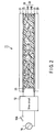
- FIG. 2 is a cross-sectional view of the light control element 11.
- the light control element 11 can take a given planar shape, for example, a square.
- the light control film is processed in accordance with an outline of a region to be attached.
- the light control element 11 includes base members 20 and 21 disposed opposite to each other, and a liquid crystal layer (light control layer) 24 disposed between the base members 20 and 21.
- the base members 20 and 21 are made of a transparent member, for example, a transparent film.
- a polyethylene terephthalate (PET) film, a polyethylene (PE) film, and a polycarbonate (PC) film can be used as the base members 20 and 21.
- the liquid crystal layer 24 includes a liquid crystal material 24A and a polymer material 24B.
- the liquid crystal layer 24 is made of polymer dispersed liquid crystal (PDLC) or polymer network liquid crystal (PNLC).
- the polymer dispersed liquid crystal is composed of a complex in which a liquid crystal material is dispersed in a matrix made of a polymer material; that is, the polymer dispersed liquid crystal has a configuration in which the liquid crystal is phase-separated in the matrix.
- the polymer network liquid crystal is composed of a complex in which a liquid crystal material having a continuous phase is filled in a three-dimensional network structure (polymer network) made of a polymer material.
- a photocurable resin can be used as the polymer material.
- a solution in which a liquid crystal material is mixed with a photopolymerization type polymer precursor (monomer) is irradiated with ultraviolet light to polymerize the monomer, thereby forming a polymer, and the liquid crystal is dispersed in the matrix made of the aforementioned polymer.
- a transparent electrode 22 is provided on the base member 20 so as to be in contact with the liquid crystal layer 24.
- a transparent electrode 23 is provided on the base member 21 so as to be in contact with the liquid crystal layer 24.
- the transparent electrodes 22 and 23 are made of a material having both light transparency and conductivity, and are made of, for example, ITO (indium tin oxide).
- the light control element 11 includes connection terminals (not shown) electrically connected to the transparent electrodes 22 and 23, respectively, and provided to enable an electrical connection to the drive circuit 12.
- the connection terminals are made of metal (e.g., gold, silver, copper, aluminum, etc.).
- the liquid crystal layer 24 is sealed between the transparent electrodes 22 and 23 by a sealing member 25.
- the sealing member 25 is formed in a manner to surround the liquid crystal layer 24.
- the sealing member 25 is made of, for example, a light curing resin.
- liquid crystal layer (light control layer) 24 Next, a broad operation of the liquid crystal layer (light control layer) 24 will be described.
- the ordinary light refractive index of the liquid crystal material and the refractive index of the polymer material are set to be approximately the same.
- the liquid crystal material for example, a positive (P-type) nematic liquid crystal having positive dielectric anisotropy is used.
- the switching element 13A is turned off, thereby stopping supply from the commercial power supply 15 to the light control element 11.
- the switching element 13A is included in the power supply circuit 13, and the operation of the switching element 13A is controlled by the control circuit 14. In this OFF state, no voltage is applied to the liquid crystal layer 24.
- liquid crystal molecules When no voltage (no electric field) is applied to the liquid crystal layer 24, liquid crystal molecules enter a random state with respect to the interface of the polymer matrix (or polymer network). In this case, the refractive indexes of the liquid crystal material and the polymer matrix differ, thereby ensuring that incident light is scattered at the interface of the polymer matrix. That is, in a state in which the liquid crystal molecules are not aligned, the liquid crystal layer 24 is in a high haze state. At this time, the liquid crystal layer 24 is in a cloudy state, while the light control element 11 is in an opaque state. In this manner, the light control element 11 can shield an object from an observer.
- the haze value is an index related to the transparency of a member and represents the degree of haze. A smaller haze value indicates a higher transparency.
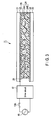
- the switching element 13A is turned on, so that the commercial power supply 15 is supplied to the light control element 11. In this ON state, a voltage is applied to the liquid crystal layer 24.
- the major axes (directors) of the liquid crystal molecules align in a direction substantially perpendicular to the electrode planes.
- the refractive index of the liquid crystal material is approximately the same as that of the polymer matrix, so that the incident light is hardly scattered in the liquid crystal layer 24 and passes through the liquid crystal layer 24. That is, in a state in which the liquid crystal molecules are aligned, the liquid crystal layer 24 is in a low haze state. At this time, the liquid crystal layer 24 is in a transparent state, and the light control element 11 is also in a transparent state. Therefore, the observer can observe an object through the light control element 11.
- This embodiment describes the case in which the light control element enters an opaque state when no current is applied, and a transparent state when a current is applied.
- the present invention is not limited to this case.
- the present invention is also applicable to a reverse type that enters a transparent state when no current is applied, and an opaque state when a current is applied.
- FIG. 4 is an equivalent circuit diagram of the light control element 11.
- the transparent electrode 22 is formed in a planar shape. Therefore, the transparent electrode 22 constitutes a plurality of resistance components R1 to R11 so as to extend from a terminal side (a side close to a terminal connected to the drive circuit 12) to a distal side (a side opposite to the terminal).
- the transparent electrode 23 is formed in a planar shape. Therefore, the transparent electrode 23 constitutes a plurality of resistance components R12 to R22 so as to extend from the terminal side to the distal side.
- the liquid crystal layer 24 constitutes a plurality of capacitance components C1 to C4 connected between the transparent electrode 22 and the transparent electrode 23.
- the voltage is high on the terminal side and decreases toward the distal side.
- FIG. 5 is a circuit diagram of the drive circuit 12.
- a node N1 is connected to the commercial power supply 15 via the power supply circuit 13.
- a voltage dividing circuit 30 is connected to the node N1.
- the voltage dividing circuit 30 includes resistors R30 and R31 connected in series between the node N1 and a ground terminal GND.
- the voltage dividing circuit 30 outputs, from a node N2, an AC voltage having the maximum value lower than that of the commercial power supply 15. For example, the voltage dividing circuit 30 reduces the voltage of the node N1 to about 1/20.
- the voltage dividing ratio of the voltage dividing circuit 30 is optimally set in accordance with the withstand voltages of a plurality of active elements connected to a subsequent stage of the voltage dividing circuit 30.
- An operational amplifier AP1 has a non-inverted input terminal connected to the node N2, and an inverted input terminal connected to an output terminal of the operational amplifier AP1 itself.
- the operational amplifier AP1 constitutes a voltage follower.
- the operational amplifier AP1 has a positive power supply terminal to which a positive voltage "+V1" is applied, and a negative power supply terminal to which a negative voltage "-V1” is applied.
- the positive voltage "+V1" is about +15 V
- the negative voltage "-V1” is about -15 V.
- a DC power supply applied to another active element described later is also the same as in the operational amplifier AP1.
- the operational amplifier AP1 has an output terminal connected to one end of a resistor R32 via a node N3. The other end of the resistor R32 is connected to a node N4.
- a voltage limiter 31 includes an operational amplifier AP2, a diode D1, and a variable power supply 32.
- the voltage limiter 31 is an upper limit limiter, and limits a positive voltage to a predetermined voltage.
- An operational amplifier AP2 has an inverted input terminal connected to the node N4, and a non-inverted input terminal connected to a positive electrode of the variable power supply 32.
- the operational amplifier AP2 has an output terminal connected to a cathode of the diode D1.
- the diode D1 has an anode connected to the node N4.
- the variable power supply 32 is a DC power supply and supplies a positive reference voltage "VrefC+" to the non-inverted input terminal of the operational amplifier AP2.
- the reference voltage "VrefC+” is variable, and the voltage limiter 31 is capable of adjusting a positive-side limit voltage in accordance with the reference voltage "VrefC+".
- the reference voltage "VrefC+” can be freely set by the control circuit 14 or a user from the outside.
- a voltage limiter 33 includes an operational amplifier AP3, a diode D2, and a variable power supply 34.
- the voltage limiter 33 is a lower limit limiter, and limits a negative voltage to a predetermined voltage.
- An operational amplifier AP3 has an inverted input terminal connected to the node N4, and a non-inverted input terminal connected to a negative electrode of the variable power supply 34.
- the operational amplifier AP3 has an output terminal connected to an anode of the diode D2.
- a cathode of the diode D2 is connected to the node N4.
- the variable power supply 34 is a DC power supply and supplies a negative reference voltage "VrefC-" to the non-inverted input terminal of the operational amplifier AP3.
- the reference voltage "VrefC-" is variable, and the voltage limiter 33 is capable of adjusting a negative-side limit voltage in accordance with the reference voltage "VrefC-".
- the reference voltage "VrefC-" can be freely set by the control circuit 14 or a user from the outside.
- An error amplifier 35 has a first input terminal connected to the node N4 and a second input terminal connected to a voltage dividing circuit 36.
- the voltage dividing circuit 36 includes resistors R33 and R34 connected in series between a feedback circuit 43 described later and a ground terminal GND.
- the voltage dividing circuit 36 outputs, from a node N5, a voltage lower than an output of the feedback circuit 43.
- the node N5 between the resistors R33 and R34 is connected to a second input terminal of the error amplifier 35.
- the voltage dividing ratio of the voltage dividing circuit 36 is set to be the same as that of the voltage dividing circuit 30.
- Each resistor included in the voltage dividing circuit 36 is set to, for example, about 1/10 of each resistor included in the voltage dividing circuit 30.
- a comparator CP1 has a non-inverted input terminal connected to the node N3 and an inverted input terminal connected to the positive electrode of the variable power supply 32.
- the comparator CP1 has an output terminal connected to a timing generation circuit 39.
- the comparator CP1 compares an output of the operational amplifier AP1 with the reference voltage "VrefC+", and sends the comparison result to the timing generation circuit 39.
- a comparator CP2 has an inverted input terminal connected to the node N3 and a non-inverted input terminal connected to the negative electrode of the variable power supply 34.
- the comparator CP2 has an output terminal connected to the timing generation circuit 39.
- the comparator CP2 compares an output of the operational amplifier AP1 with the reference voltage "VrefC-", and sends the comparison result to the timing generation circuit 39.
- a comparator CP3 has a non-inverted input terminal connected to the node N3 and an inverted input terminal connected to the ground terminal GND. Voltage of 0 V is applied to the ground terminal GND.
- the comparator CP3 has an output terminal connected to the timing generation circuit 39.
- the comparator CP3 constitutes a zero crossing circuit. That is, the comparator CP3 detects a point (the "zero crossing point") at which a voltage of the AC power supply becomes zero.
- the transistors (switching elements) T1 and T2 are formed of MOS transistors or bipolar transistors. Described in the present embodiment is an example in which an N-channel MOS transistor (or a power MOS transistor), for example, is used as the transistors T1 and T2.
- the transistor T1 has a drain connected to the node N1, a source connected to a source of the transistor T2, and a gate connected to a gate driver 41.
- the transistor T2 has a drain connected to a low pass filter LPF via a node N6, and a gate connected to a gate driver 42.
- a diode (also called a “feedback diode”) D3 as a rectifying element is connected in parallel to the transistor T1.
- the diode D3 has an anode connected to the source of the transistor T1, and a cathode connected to a drain of the transistor T1.
- a diode D4 is connected in parallel to the transistor T2.
- the diode D4 has an anode connected to a source of the transistor T2, and a cathode connected to a drain of the transistor T2.
- the transistor T1 When the transistor T1 is formed of a MOS transistor, a parasitic diode of the MOS transistor T1 plays a role of the diode D3, thereby eliminating the need to newly add the diode D3.
- the transistor T2 when the transistor T2 is formed of a MOS transistor, a parasitic diode of the MOS transistor T2 plays a role of the diode D4, thereby eliminating the need to newly add the diode D4.
- the transistors T1 and T2 are formed of bipolar transistors, the diodes D3 and D4 are connected in parallel to the bipolar transistors T1 and T2, respectively.
- the low pass filter LPF includes an inductor L and a capacitor C. That is, the low pass filter LPF is formed of an LC low pass filter.
- the inductor L has one end connected to node N6 and the other end connected to one electrode of the capacitor C via a node N7.
- the other electrode of the capacitor C is connected to the ground terminal GND.
- the light control element 11 is connected between the node N7 and the ground terminal GND.
- the light control element 11 includes a resistive load RL and a capacitive load CL, as understood from FIG. 4 .
- the feedback circuit 43 is connected in parallel to the inductor L via the nodes N6 and N7.
- the feedback circuit 43 detects a voltage of the inductor L, and feeds back the detected voltage to the error amplifier 35 via the voltage dividing circuit 36.
- a voltage of the inductor L substantially corresponds to a voltage applied to the light control element 11.
- the error amplifier 35 amplifies a difference between a voltage of the node N4 and that of the node N5. An output of the error amplifier 35 is sent to a PWM circuit 37.
- a voltage of the node N4 is an AC voltage substantially corresponding to an AC voltage obtained by multiplying an AC voltage of the commercial power supply 15 by, for example, 1/20.
- a voltage of the node N5 is a voltage substantially corresponding to a voltage obtained by multiplying a voltage of the inductor L by, for example, 1/20.
- An output of the error amplifier 35 is sent to a PWM circuit 37.
- the PWM circuit 37 performs PWM control using an output of the error amplifier 35.
- Pulse width modulation is a method of changing the width (pulse width) of a pulse signal without changing the frequency of the pulse signal.
- the PWM circuit 37 decreases the pulse width when an output (error) of the error amplifier 35 is large, and increases the pulse width when an output of the error amplifier 35 is small. That is, the PWM circuit 37 includes a high frequency oscillator, and controls the duty ratio of a pulse signal by using an output of the error amplifier 35.
- Pulse frequency modulation is a method of changing the frequency of a pulse signal without changing the pulse width.
- PFM control is applied, the frequency of the pulse signal is made low in a period during which further reduction of voltage is desired.
- a thinning circuit 40 controls timing for thinning out a partial period (cycle) of an AC voltage (AC waveform). That is, the drive circuit 12 is capable of partially or periodically thinning an AC waveform applied to the light control element 11. An output of the thinning circuit 40 is sent to the timing generation circuit 39. Operations of the thinning circuit 40 will be described in the second embodiment.
- the timing generation circuit 39 controls timing for generating a pulse signal for PWM control by using outputs of the comparators CP1 to CP3 and an output of the thinning circuit 40. An output of the timing generation circuit 39 is sent to a PWM switching circuit 38.
- the PWM switching circuit 38 executes control to switch between periods in which the PWM control is performed and not performed. In a period in which the PWM control is performed, the PWM switching circuit 38 executes the PWM control (that is, control of the pulse width) using the output of the PWM circuit 37. In a period in which the PWM control is not performed, the PWM switching circuit 38 does not execute the PWM control (that is, the transistor T1 or the transistor T2 is turned on) regardless of the output of the PWM circuit 37.
- the gate driver 41 applies a gate voltage to the transistor T1 based on the control of the PWM switching circuit 38 to control the switching operation of the transistor T1.
- the gate driver 42 applies a gate voltage to the transistor T2 based on the control of the PWM switching circuit 38 to control the switching operation of the transistor T2.
- the voltage levels of the gate drivers 41 and 42 are optimally set in accordance with the characteristics of transistors T1 and T2, respectively.
- FIG. 6 is a diagram for explaining an AC waveform of the commercial power supply 15.
- the commercial power supply 15 has a positive maximum value "+Vm”, a negative minimum value "-Vm”, and a cycle T.
- the withstand voltage of the light control element 11 is defined in accordance with the characteristics of its components, in particular, the characteristics of the liquid crystal layer 24.
- the parts shown by the arrows in FIG. 6 are parts in which the commercial power supply 15 exceeds the withstand voltage of the light control element 11.
- an AC voltage applied to the light control element 11 is controlled so as to be no less than the limit voltage "-Vc" and no more than the limit voltage "+Vc".
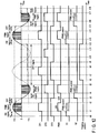
- FIG. 7 is a timing chart for explaining the operation of the drive circuit 12.
- a voltage of the commercial power supply 15 becomes 0 V and then transits to the positive side.
- the comparator CP3 for zero crossing detects that a voltage of the commercial power supply 15 has reached 0 V, and outputs a high level.
- the gate driver 41 outputs a high level as a signal S1. This turns on the transistor T1.
- the comparator CP1 At time t1, when a voltage of the commercial power supply 15 becomes higher than the positive limit voltage "+Vc", the comparator CP1 outputs a high level.
- the reference voltage "VrefC+” applied from the variable power supply 32 to the comparator CP1 is set to about 1/20 of the limit voltage "+Vc”.
- the PWM switching circuit 38 turns on the PWM control. That is, the PWM switching circuit 38 sends a pulse signal for PWM control to the gate driver 41.
- the gate driver 41 supplies a pulse signal as the signal S1 to the gate of the transistor T1.
- the pulse width (duty ratio) of the signal S1 is controlled by the PWM circuit 37.
- the comparator CP1 outputs a low level.
- the PWM switching circuit 38 turns off the PWM control.
- the gate driver 41 outputs a low level as the signal S1. This turns off the transistor T1.
- the applied voltage of the light control element 11 is maintained by a capacitive load CL of the light control element 11.
- a voltage of the commercial power supply 15 becomes 0 V and then transits to the negative side.
- the comparator CP3 for zero crossing detects that a voltage of the commercial power supply 15 has become 0 V, and outputs a low level.
- the gate driver 42 outputs a high level as a signal S2. This turns on the transistor T2.
- the comparator CP2 outputs a high level.
- the reference voltage "VrefC-" applied from the variable power supply 34 to the comparator CP2 is set to about 1/20 of the limit voltage "-Vc”.
- the PWM switching circuit 38 turns on the PWM control. That is, the PWM switching circuit 38 sends a pulse signal for PWM control to the gate driver 42.
- the gate driver 42 supplies a pulse signal as the signal S2 to the gate of the transistor T2.
- the pulse width (duty ratio) of the signal S2 is controlled by the PWM circuit 37.
- the comparator CP2 outputs a low level.
- the PWM switching circuit 38 turns off the PWM control.
- the gate driver 42 outputs a low level as the signal S2. This turns off the transistor T2. After the transistor T2 is turned off, a voltage applied to the light control element 11 is maintained by a capacitive load CL of the light control element 11.
- a voltage of the commercial power supply 15 becomes 0 V and then transits to the positive side.
- the comparator CP3 for zero crossing outputs a high level. Thereafter, a similar control is performed, and the drive circuit 12 converts a voltage of the commercial power supply 15 into an AC voltage that varies within a range between the limit voltage "-Vc" and the limit voltage "+Vc".
- FIG. 8 is a diagram for explaining an AC voltage applied to the light control element 11.
- a pulse voltage generated by the transistor T1 is smoothed out by the low pass filter LPF, and set to be approximately equal to the limit voltage "+Vc". The same applies to the limit voltage "-Vc".
- An AC voltage that varies within a range between the limit voltage "+Vc” and the limit voltage "-Vc” is then applied to the light control element 11.
- FIG. 9 is a timing chart for explaining an operation of the drive circuit 12 according to the modification of the first embodiment.
- the reference voltage "VrefC+" of the variable power supply 32 is optimally set in accordance with the limit voltage "+Vc"
- the reference voltage "VrefC-" of the variable power supply 34 is optimally set in accordance with the limit voltage "-Vc”.
- the period from t1 to t2 corresponding to the PWM region is longer in the modification than that of the first embodiment shown in FIG. 7 .
- the period from t4 to t5 corresponding to the PWM region is longer in the modification than that of the first embodiment shown in FIG. 7 .
- the limit voltage "+Vc" in the modification can be made lower than that of the first embodiment shown in FIG. 7 . Furthermore, the limit voltage "-Vc" in the modification can be made higher than that of the first embodiment shown in FIG. 7 .
- the other operations are the same as the operations of the first embodiment described above.
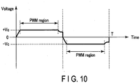
- FIG. 10 is a diagram for explaining an AC voltage applied to the light control element 11 according to the modification.
- a pulse voltage is smoothed out by the low pass filter LPF and is set to be approximately equal to the limit voltage "+Vc". The same applies to the limit voltage "-Vc". Then, an AC voltage having a smaller amplitude than that of the first embodiment shown in FIG. 8 is applied to the light control element 11.
- FIG. 11 is a set of graphs showing an example of V-T characteristics of the light control element 11.
- the horizontal axis presents a voltage (V) while the vertical axis presents a transmittance (%), and both axes adopt arbitrary units.
- the voltage shown in FIG. 11 is an effective voltage of the AC power supply.
- FIG. 11 shows four graphs obtained by changing the frequency of the AC power supply; that is, a graph with the frequency of 1Hz, a graph with the frequency of 30Hz, a graph with the frequency of 60Hz, and a graph with the frequency of 100Hz.
- the transmittance of the light control element 11 can be altered by changing the effective voltage applied to the light control element 11. Furthermore, the transmittance of the light control element 11 can be altered at will by changing the frequency of the AC power supply.
- the limit voltages are defined with consideration towards the withstand voltage of the light control element 11.
- the transmittance of the light control element 11 can be altered at will by changing the voltages "+Vc" and "-Vc" within the range lower than the withstand voltage of the light control element 11.
- the transmittance of the light control element 11 can be altered at will by changing the frequency of the AC power supply.
- the voltage "+Vc” can be altered by changing the reference voltage "VrefC+” of the variable power supply 32
- the voltage "-Vc” can be altered by changing the reference voltage "VrefC-" of the variable power supply 34.
- the light control device 10 includes: the light control element 11 including a polymer dispersed liquid crystal or a polymer network liquid crystal; the transistors (switching elements) T1 and T2 connected in series between the commercial power supply 15 and the light control element 11; the diode (rectifying element) D3 connected in parallel to the transistor T1 and connected in the forward direction from the light control element 11 to the commercial power supply 15; and the diode (rectifying element) D4 connected in parallel to the transistor T2 and connected in the forward direction from the commercial power supply 15 to the light control element 11.
- the light control element 11 including a polymer dispersed liquid crystal or a polymer network liquid crystal
- the transistors (switching elements) T1 and T2 connected in series between the commercial power supply 15 and the light control element 11
- the diode (rectifying element) D3 connected in parallel to the transistor T1 and connected in the forward direction from the light control element 11 to the commercial power supply 15
- the diode (rectifying element) D4 connected in parallel to the transistor T2 and
- the PWM switching circuit (control circuit) 38 is configured to perform the PWM control or PFM control on the transistor T1 when a voltage of the commercial power supply 15 is higher than the limit voltage "+Vc" that is higher than 0 V and is lower than the maximum value of the commercial power supply 15, and to perform the PWM control or PFM control on the transistor T2 when a voltage of the commercial power supply 15 is lower than the limit voltage "-Vc" that is higher than the minimum value of the commercial power supply 15 and is lower than 0 V.
- the light control device 10 can be driven using the commercial power supply 15 that is a general power supply supplied from an electric power company, etc., for industrial use or household use.
- the commercial power supply 15 that is a general power supply supplied from an electric power company, etc., for industrial use or household use.
- deterioration of the liquid crystal layer 24 included in the light control element 11 can be suppressed.
- an AC waveform is generated in an analog manner using analog elements, power consumption increases and the amount of heat generation increases.
- the amplitude of an AC voltage is made small using the PWM control, so that power consumption can be reduced and the amount of heat generation can also be reduced.
- the comparator CP1 is caused to compare the reference voltage "VrefC+" of the variable power supply 32 with the AC voltage obtained by stepping down the commercial power supply 15, and based on this comparison result, a voltage lower than the limit voltage "+Vc" is applied to the light control element 11. Therefore, the limit voltage "+Vc" can be altered at will by changing the reference voltage "VrefC+". As a result, the transmittance of the light control element 11 can be changed at will.
- the commercial power supply 15 is used without any change for a voltage between the limit voltage "+Vc" and the limit voltage "-Vc". Accordingly, the power loss can be further reduced.
- the second embodiment is configured in a manner such that an AC voltage is partially or periodically thinned out.
- FIG. 12 is a timing chart for explaining operations of the drive circuit 12 according to the second embodiment of the present invention.
- the operations from time t0 to time t6 are the same as the operations of the first embodiment shown in FIG. 7 .
- the thinning circuit 40 receives an output of the comparator CP3 for detecting zero crossing.
- the thinning circuit 40 sends a thinning pattern to the timing generation circuit 39.
- the thinning circuit 40 outputs a low level as a thinning pattern from time t0 to time t6. For example, when the thinning pattern is a low level, the timing generation circuit 39 generates a signal for causing the transistors T1 and T2 to perform switching operations.
- the comparator CP3 for zero crossing outputs a high level.
- the thinning circuit 40 outputs a high level as a thinning pattern.
- the timing generation circuit 39 turns off the transistors T1 and T2 in a period in which the thinning pattern is a high level. In a period in which the transistors T1 and T2 are turned off, a voltage applied to the light control element 11 is maintained by the capacitive load CL of the light control element 11.
- the comparator CP3 for zero crossing outputs a high level.
- the thinning circuit 40 outputs a low level as a thinning pattern.
- the timing generation circuit 39 generates a signal for causing the transistors T1 and T2 to perform switching operations. Accordingly, an AC voltage is applied to the light control element 11. Thereafter, the similar control is performed, and the drive circuit 12 converts a voltage of the commercial power supply 15 into an AC voltage that varies within a range between the limit voltage "-Vc" and the limit voltage "+Vc".
- a period in which the commercial power supply 15 is thinned out (that is, a thinning pattern by the thinning circuit 40) can be freely set.
- an AC voltage may be thinned every other cycle, that is, an AC voltage may be thinned only for one of two cycles.
- a waveform having a frequency equal to half of a frequency of the commercial power supply 15 can be generated.
- an AC voltage having a frequency of 30Hz can be generated.
- an AC voltage may be thinned for one cycle every two cycles; that is, an AC voltage may be thinned only for one of three cycles.
- the thinning circuit 40 counts the number of rising edges of output of the comparator CP3 for zero crossing and sets a period for thinning out an AC voltage in accordance with a count value.
- power consumption of the transistors T1 and T2 can be reduced in a period in which an AC voltage is thinned out. This achieves a reduction of power consumption of the light control device 10.
- a time period in which the transistors (MOS transistors) T1 and T2 are turned on can be shortened by thinning out an AC voltage. This makes it possible to decrease the size of the MOS transistors T1 and T2.
- the MOS transistors decreased in size require less power consumption and less heat generation, thereby realizing the reduction of the power consumption and the amount of heat generation of the light control device 10.
- the other effects are the same as those in the first embodiment.
- the liquid crystal element (light control element) using PDLC or PNLC has been described as an example; however, the present invention is not limited to this.
- the liquid crystal element may have a configuration in which a polarizing plate and an alignment film are disposed on both sides of a liquid crystal layer, and may employ a TN (Twisted Nematic) method, a VA (Vertical Alignment) method, an IPS (In-Plane Switching) method, etc.
- TN Transmission Nematic
- VA Very Alignment
- IPS In-Plane Switching
- the switching elements T1 and T2 described in each of the above embodiments may be formed of a SiC-MOSFET using silicon carbide (SiC) for a semiconductor layer, a GaN-MOSFET using gallium nitride (GaN) for a semiconductor layer, etc.
- the rectifying elements D3 and D4 described in each of the above embodiments may be formed of, other than the diode, a Schottky diode, a fast recovery diode (FRD), a SiC diode, a GaN diode, a MOS diode, etc.
- the light control device described in each of the above embodiments is applicable to windows and indoor partitions in homes, offices or public facilities, image projection screens and signage in commercial facilities or event venues, windows and sunroofs in vehicles (cars) or aircrafts, etc.
- an AC power supply is generated using a D/A converter.
- the light control device according to the present embodiment is also applicable to an AC power supply obtained by converting a DC power supply.
- the light control element has been described as an example of the liquid crystal element.
- the present invention is not limited thereto, and is applicable to various devices (including a liquid crystal display device) using liquid crystal.
- the present invention is not limited to the above-mentioned embodiments, and can be reduced to practice by modifying the constituent elements without departing from the spirit and scope of the invention.
- the above-described embodiments include inventions of various stages, and a variety of inventions can be derived by properly combining structural elements of one embodiment or by properly combining structural elements of different embodiments. For example, if the object of the invention is achieved and the advantages of the invention are attained even after some of the structural elements disclosed in connection with the embodiments are deleted, the structure made up of the resultant structural elements can be extracted as an invention.
Landscapes
- Physics & Mathematics (AREA)
- Nonlinear Science (AREA)
- Crystallography & Structural Chemistry (AREA)
- Engineering & Computer Science (AREA)
- Chemical & Material Sciences (AREA)
- General Physics & Mathematics (AREA)
- Optics & Photonics (AREA)
- Mathematical Physics (AREA)
- Power Engineering (AREA)
- Computer Hardware Design (AREA)
- Theoretical Computer Science (AREA)
- Liquid Crystal (AREA)
- Liquid Crystal Display Device Control (AREA)
- Circuit Arrangement For Electric Light Sources In General (AREA)
Abstract
Description
- The present invention generally relates to a light control device using a liquid crystal.
- There is known a light control device using a polymer dispersed liquid crystal or a polymer network liquid crystal capable of performing bright display without necessarily requiring alignment processing and with no need for a polarizing plate. A liquid crystal layer (light control layer) includes a liquid crystal material and a polymer material. The ordinary light refractive index of the liquid crystal material and the refractive index of the polymer material are set to be approximately the same.
- The light control device is, for example, in a scattering state when a voltage is not applied to the liquid crystal layer, and in a transmissive state when a voltage is applied to the liquid crystal layer. For the light control device, for example, it is desirable to use a commercial power supply (effective voltage of 100 V, frequency of 60Hz or 50Hz) when considering its use in the home or workplace. However, since the crest value (maximum value) of a commercial power supply is 100√2 V, the light control device cannot be driven when the withstand voltage of the liquid crystal layer is lower than the crest value of the commercial power supply.
- To address this, one option is to reduce a commercial power supply using a variable auto-transformer called "slidac" and drive the light control device using a reduced AC power supply. In this case, the light control device is increased in both size and weight.
- Another option is to convert a commercial power supply into a direct current with an AC/DC power supply circuit, and then drive the light control device using this direct current voltage. In this case, the power supply sees a decrease in conversion efficiency, and the light control device sees an increase in power consumption.
- The present invention provides a light control device capable of reducing power consumption.
- According to a first aspect of the present invention, there is provided a light control device comprising:
- a light control element including a first layer stack and a second layer stack which include electrodes provided on base members, respectively, and a liquid crystal layer sandwiched between the first and second layer stacks;
- a first switching element connected between an AC power supply and the light control element;
- a first comparator that detects whether or not the AC power supply is higher than a first voltage that is higher than 0 V and is lower than a maximum value of the AC power supply; and
- a control circuit that performs PWM (pulse width modulation) control or PFM (pulse frequency modulation) control on the first switching element if the AC power supply is higher than the first voltage.
- According to the present invention, it is possible to provide a light control device capable of reducing power consumption.
-
-
FIG. 1 is a block diagram of a light control device according to a first embodiment. -
FIG. 2 is a cross-sectional view of a light control element. -
FIG. 3 is a cross-sectional view for explaining the alignment of a liquid crystal layer. -
FIG. 4 is an equivalent circuit diagram of the light control element. -
FIG. 5 is a circuit diagram of a drive circuit. -
FIG. 6 is a diagram for explaining an AC waveform of a commercial power supply. -
FIG. 7 is a timing chart for explaining operations of the drive circuit according to the first embodiment. -
FIG. 8 is a diagram for explaining an AC voltage applied to the light control element according to the first embodiment. -
FIG. 9 is a timing chart for explaining operations of a drive circuit according to a modification. -
FIG. 10 is a diagram for explaining an AC voltage applied to a light control element according to the modification. -
FIG. 11 is a set of graphs showing an example of V-T characteristics of the light control element. -
FIG. 12 is a timing chart for explaining operations of a drive circuit according to a second embodiment. - A description will now be given of the embodiments with reference to the accompanying drawings. It should be noted that the drawings are schematic or conceptual, and the dimensions and scales of the drawings are not necessarily the same as the actual products. Where the same portion is depicted in different drawings, the dimensions and scale of one drawing may be different from those of another. Several embodiments described below merely show exemplary apparatuses and methods that implement the technical ideas of the present invention. The technical ideas are not limited by the element shapes, structures, arrangements, etc. described below. In the description below, structural elements having substantially the same functions and configurations will be denoted by the same reference symbols, and a repetitive description of such elements will be given only where necessary.
-
FIG. 1 is a block diagram of alight control device 10 according to a first embodiment of the present invention. Thelight control device 10 includes alight control element 11, adrive circuit 12, apower supply circuit 13, and acontrol circuit 14. - The
light control element 11 is an element capable of controlling the light transmittance. Thelight control element 11 is made of, for example, a light control film. The light control film is a functional film capable of instantly switching between transparency and opacity (white turbidity) depending on the power being on/off. An example of the configuration of thelight control element 11 will be described later. - The
drive circuit 12 applies a voltage to thelight control element 11 to drive thelight control element 11. The circuit configuration of thedrive circuit 12 will be described later. - The
power supply circuit 13 receives an AC power supply from the outside. As an example, in the present embodiment, a commercial AC power supply (commercial power supply) is adopted as the AC power supply. The commercial power supply is a general power supply supplied from an electric power company or the like for industrial use or household use. It is an AC power supply. The commercial power supply has the effective voltage of 100 V, the crest value (maximum value) of 100V2 V, and the frequency of 60Hz or 50Hz. Thepower supply circuit 13 supplies a commercial power supply to thelight control element 11. Furthermore, thepower supply circuit 13 generates a predetermined voltage (DC voltage) to be used as a power supply for an active element included in thedrive circuit 12, and supplies this DC voltage to thedrive circuit 12. - The
control circuit 14 controls thedrive circuit 12 and thepower supply circuit 13. Thecontrol circuit 14 supplies control signals to thedrive circuit 12 and thepower supply circuit 13, so that thedrive circuit 12 and thepower supply circuit 13 can perform desired operations. - Next, the configuration of the
light control element 11 will be described.FIG. 2 is a cross-sectional view of thelight control element 11. Thelight control element 11 can take a given planar shape, for example, a square. When thelight control element 11 is a light control film, the light control film is processed in accordance with an outline of a region to be attached. - The
light control element 11 includesbase members 20 and 21 disposed opposite to each other, and a liquid crystal layer (light control layer) 24 disposed between thebase members 20 and 21. Thebase members 20 and 21 are made of a transparent member, for example, a transparent film. For example, a polyethylene terephthalate (PET) film, a polyethylene (PE) film, and a polycarbonate (PC) film can be used as thebase members 20 and 21. - The
liquid crystal layer 24 includes aliquid crystal material 24A and apolymer material 24B. Theliquid crystal layer 24 is made of polymer dispersed liquid crystal (PDLC) or polymer network liquid crystal (PNLC). The polymer dispersed liquid crystal is composed of a complex in which a liquid crystal material is dispersed in a matrix made of a polymer material; that is, the polymer dispersed liquid crystal has a configuration in which the liquid crystal is phase-separated in the matrix. The polymer network liquid crystal is composed of a complex in which a liquid crystal material having a continuous phase is filled in a three-dimensional network structure (polymer network) made of a polymer material. As the polymer material, a photocurable resin can be used. For example, in PDLC, a solution in which a liquid crystal material is mixed with a photopolymerization type polymer precursor (monomer) is irradiated with ultraviolet light to polymerize the monomer, thereby forming a polymer, and the liquid crystal is dispersed in the matrix made of the aforementioned polymer. - A
transparent electrode 22 is provided on the base member 20 so as to be in contact with theliquid crystal layer 24. Atransparent electrode 23 is provided on thebase member 21 so as to be in contact with theliquid crystal layer 24. Thetransparent electrodes - The
light control element 11 includes connection terminals (not shown) electrically connected to thetransparent electrodes drive circuit 12. The connection terminals are made of metal (e.g., gold, silver, copper, aluminum, etc.). - The
liquid crystal layer 24 is sealed between thetransparent electrodes member 25. The sealingmember 25 is formed in a manner to surround theliquid crystal layer 24. The sealingmember 25 is made of, for example, a light curing resin. - Next, a broad operation of the liquid crystal layer (light control layer) 24 will be described.
- In the
liquid crystal layer 24, the ordinary light refractive index of the liquid crystal material and the refractive index of the polymer material are set to be approximately the same. As the liquid crystal material, for example, a positive (P-type) nematic liquid crystal having positive dielectric anisotropy is used. - As shown in
FIG. 2 , the switchingelement 13A is turned off, thereby stopping supply from thecommercial power supply 15 to thelight control element 11. The switchingelement 13A is included in thepower supply circuit 13, and the operation of theswitching element 13A is controlled by thecontrol circuit 14. In this OFF state, no voltage is applied to theliquid crystal layer 24. - When no voltage (no electric field) is applied to the
liquid crystal layer 24, liquid crystal molecules enter a random state with respect to the interface of the polymer matrix (or polymer network). In this case, the refractive indexes of the liquid crystal material and the polymer matrix differ, thereby ensuring that incident light is scattered at the interface of the polymer matrix. That is, in a state in which the liquid crystal molecules are not aligned, theliquid crystal layer 24 is in a high haze state. At this time, theliquid crystal layer 24 is in a cloudy state, while thelight control element 11 is in an opaque state. In this manner, thelight control element 11 can shield an object from an observer. The haze value is an index related to the transparency of a member and represents the degree of haze. A smaller haze value indicates a higher transparency. - On the other hand, as shown in
FIG. 3 , the switchingelement 13A is turned on, so that thecommercial power supply 15 is supplied to thelight control element 11. In this ON state, a voltage is applied to theliquid crystal layer 24. - When a voltage is applied to the
liquid crystal layer 24, the major axes (directors) of the liquid crystal molecules align in a direction substantially perpendicular to the electrode planes. In this case, the refractive index of the liquid crystal material is approximately the same as that of the polymer matrix, so that the incident light is hardly scattered in theliquid crystal layer 24 and passes through theliquid crystal layer 24. That is, in a state in which the liquid crystal molecules are aligned, theliquid crystal layer 24 is in a low haze state. At this time, theliquid crystal layer 24 is in a transparent state, and thelight control element 11 is also in a transparent state. Therefore, the observer can observe an object through thelight control element 11. - This embodiment describes the case in which the light control element enters an opaque state when no current is applied, and a transparent state when a current is applied. However, the present invention is not limited to this case. The present invention is also applicable to a reverse type that enters a transparent state when no current is applied, and an opaque state when a current is applied.
- Next, an equivalent circuit of the
light control element 11 will be described.FIG. 4 is an equivalent circuit diagram of thelight control element 11. - The
transparent electrode 22 is formed in a planar shape. Therefore, thetransparent electrode 22 constitutes a plurality of resistance components R1 to R11 so as to extend from a terminal side (a side close to a terminal connected to the drive circuit 12) to a distal side (a side opposite to the terminal). - Similarly, the
transparent electrode 23 is formed in a planar shape. Therefore, thetransparent electrode 23 constitutes a plurality of resistance components R12 to R22 so as to extend from the terminal side to the distal side. - The
liquid crystal layer 24 constitutes a plurality of capacitance components C1 to C4 connected between thetransparent electrode 22 and thetransparent electrode 23. - As can be understood from
FIG. 4 , in thelight control element 11, the voltage is high on the terminal side and decreases toward the distal side. - Next, the configuration of the
drive circuit 12 will be described.FIG. 5 is a circuit diagram of thedrive circuit 12. - A node N1 is connected to the
commercial power supply 15 via thepower supply circuit 13. To the node N1, avoltage dividing circuit 30 is connected. Thevoltage dividing circuit 30 includes resistors R30 and R31 connected in series between the node N1 and a ground terminal GND. Thevoltage dividing circuit 30 outputs, from a node N2, an AC voltage having the maximum value lower than that of thecommercial power supply 15. For example, thevoltage dividing circuit 30 reduces the voltage of the node N1 to about 1/20. The voltage dividing ratio of thevoltage dividing circuit 30 is optimally set in accordance with the withstand voltages of a plurality of active elements connected to a subsequent stage of thevoltage dividing circuit 30. - An operational amplifier AP1 has a non-inverted input terminal connected to the node N2, and an inverted input terminal connected to an output terminal of the operational amplifier AP1 itself. The operational amplifier AP1 constitutes a voltage follower. The operational amplifier AP1 has a positive power supply terminal to which a positive voltage "+V1" is applied, and a negative power supply terminal to which a negative voltage "-V1" is applied. For example, the positive voltage "+V1" is about +15 V, while the negative voltage "-V1" is about -15 V. A DC power supply applied to another active element described later is also the same as in the operational amplifier AP1.
- The operational amplifier AP1 has an output terminal connected to one end of a resistor R32 via a node N3. The other end of the resistor R32 is connected to a node N4.
- A
voltage limiter 31 includes an operational amplifier AP2, a diode D1, and avariable power supply 32. Thevoltage limiter 31 is an upper limit limiter, and limits a positive voltage to a predetermined voltage. An operational amplifier AP2 has an inverted input terminal connected to the node N4, and a non-inverted input terminal connected to a positive electrode of thevariable power supply 32. The operational amplifier AP2 has an output terminal connected to a cathode of the diode D1. The diode D1 has an anode connected to the node N4. Thevariable power supply 32 is a DC power supply and supplies a positive reference voltage "VrefC+" to the non-inverted input terminal of the operational amplifier AP2. The reference voltage "VrefC+" is variable, and thevoltage limiter 31 is capable of adjusting a positive-side limit voltage in accordance with the reference voltage "VrefC+". The reference voltage "VrefC+" can be freely set by thecontrol circuit 14 or a user from the outside. - A
voltage limiter 33 includes an operational amplifier AP3, a diode D2, and avariable power supply 34. Thevoltage limiter 33 is a lower limit limiter, and limits a negative voltage to a predetermined voltage. An operational amplifier AP3 has an inverted input terminal connected to the node N4, and a non-inverted input terminal connected to a negative electrode of thevariable power supply 34. The operational amplifier AP3 has an output terminal connected to an anode of the diode D2. A cathode of the diode D2 is connected to the node N4. Thevariable power supply 34 is a DC power supply and supplies a negative reference voltage "VrefC-" to the non-inverted input terminal of the operational amplifier AP3. The reference voltage "VrefC-" is variable, and thevoltage limiter 33 is capable of adjusting a negative-side limit voltage in accordance with the reference voltage "VrefC-". The reference voltage "VrefC-" can be freely set by thecontrol circuit 14 or a user from the outside. - An
error amplifier 35 has a first input terminal connected to the node N4 and a second input terminal connected to avoltage dividing circuit 36. Thevoltage dividing circuit 36 includes resistors R33 and R34 connected in series between afeedback circuit 43 described later and a ground terminal GND. Thevoltage dividing circuit 36 outputs, from a node N5, a voltage lower than an output of thefeedback circuit 43. The node N5 between the resistors R33 and R34 is connected to a second input terminal of theerror amplifier 35. The voltage dividing ratio of thevoltage dividing circuit 36 is set to be the same as that of thevoltage dividing circuit 30. Each resistor included in thevoltage dividing circuit 36 is set to, for example, about 1/10 of each resistor included in thevoltage dividing circuit 30. - A comparator CP1 has a non-inverted input terminal connected to the node N3 and an inverted input terminal connected to the positive electrode of the
variable power supply 32. The comparator CP1 has an output terminal connected to atiming generation circuit 39. The comparator CP1 compares an output of the operational amplifier AP1 with the reference voltage "VrefC+", and sends the comparison result to thetiming generation circuit 39. - A comparator CP2 has an inverted input terminal connected to the node N3 and a non-inverted input terminal connected to the negative electrode of the
variable power supply 34. The comparator CP2 has an output terminal connected to thetiming generation circuit 39. The comparator CP2 compares an output of the operational amplifier AP1 with the reference voltage "VrefC-", and sends the comparison result to thetiming generation circuit 39. - A comparator CP3 has a non-inverted input terminal connected to the node N3 and an inverted input terminal connected to the ground terminal GND. Voltage of 0 V is applied to the ground terminal GND. The comparator CP3 has an output terminal connected to the
timing generation circuit 39. The comparator CP3 constitutes a zero crossing circuit. That is, the comparator CP3 detects a point (the "zero crossing point") at which a voltage of the AC power supply becomes zero. - The transistors (switching elements) T1 and T2 are formed of MOS transistors or bipolar transistors. Described in the present embodiment is an example in which an N-channel MOS transistor (or a power MOS transistor), for example, is used as the transistors T1 and T2.
- The transistor T1 has a drain connected to the node N1, a source connected to a source of the transistor T2, and a gate connected to a
gate driver 41. The transistor T2 has a drain connected to a low pass filter LPF via a node N6, and a gate connected to agate driver 42. - A diode (also called a "feedback diode") D3 as a rectifying element is connected in parallel to the transistor T1. The diode D3 has an anode connected to the source of the transistor T1, and a cathode connected to a drain of the transistor T1. Similarly, a diode D4 is connected in parallel to the transistor T2. The diode D4 has an anode connected to a source of the transistor T2, and a cathode connected to a drain of the transistor T2.
- When the transistor T1 is formed of a MOS transistor, a parasitic diode of the MOS transistor T1 plays a role of the diode D3, thereby eliminating the need to newly add the diode D3. Similarly, when the transistor T2 is formed of a MOS transistor, a parasitic diode of the MOS transistor T2 plays a role of the diode D4, thereby eliminating the need to newly add the diode D4. When the transistors T1 and T2 are formed of bipolar transistors, the diodes D3 and D4 are connected in parallel to the bipolar transistors T1 and T2, respectively.
- The low pass filter LPF includes an inductor L and a capacitor C. That is, the low pass filter LPF is formed of an LC low pass filter. The inductor L has one end connected to node N6 and the other end connected to one electrode of the capacitor C via a node N7. The other electrode of the capacitor C is connected to the ground terminal GND.
- The
light control element 11 is connected between the node N7 and the ground terminal GND. When expressed as an equivalent circuit, thelight control element 11 includes a resistive load RL and a capacitive load CL, as understood fromFIG. 4 . - The
feedback circuit 43 is connected in parallel to the inductor L via the nodes N6 and N7. Thefeedback circuit 43 detects a voltage of the inductor L, and feeds back the detected voltage to theerror amplifier 35 via thevoltage dividing circuit 36. A voltage of the inductor L substantially corresponds to a voltage applied to thelight control element 11. - The
error amplifier 35 amplifies a difference between a voltage of the node N4 and that of the node N5. An output of theerror amplifier 35 is sent to aPWM circuit 37. A voltage of the node N4 is an AC voltage substantially corresponding to an AC voltage obtained by multiplying an AC voltage of thecommercial power supply 15 by, for example, 1/20. A voltage of the node N5 is a voltage substantially corresponding to a voltage obtained by multiplying a voltage of the inductor L by, for example, 1/20. An output of theerror amplifier 35 is sent to aPWM circuit 37. - The
PWM circuit 37 performs PWM control using an output of theerror amplifier 35. Pulse width modulation (PWM) is a method of changing the width (pulse width) of a pulse signal without changing the frequency of the pulse signal. ThePWM circuit 37 decreases the pulse width when an output (error) of theerror amplifier 35 is large, and increases the pulse width when an output of theerror amplifier 35 is small. That is, thePWM circuit 37 includes a high frequency oscillator, and controls the duty ratio of a pulse signal by using an output of theerror amplifier 35. - In the present embodiment, the PWM control has been described as an example; however, the present invention is not limited to this, and PFM control may be applied. Pulse frequency modulation (PFM) is a method of changing the frequency of a pulse signal without changing the pulse width. When the PFM control is applied, the frequency of the pulse signal is made low in a period during which further reduction of voltage is desired.
- A thinning
circuit 40 controls timing for thinning out a partial period (cycle) of an AC voltage (AC waveform). That is, thedrive circuit 12 is capable of partially or periodically thinning an AC waveform applied to thelight control element 11. An output of the thinningcircuit 40 is sent to thetiming generation circuit 39. Operations of the thinningcircuit 40 will be described in the second embodiment. - The
timing generation circuit 39 controls timing for generating a pulse signal for PWM control by using outputs of the comparators CP1 to CP3 and an output of the thinningcircuit 40. An output of thetiming generation circuit 39 is sent to aPWM switching circuit 38. - By using the output of the
timing generation circuit 39, thePWM switching circuit 38 executes control to switch between periods in which the PWM control is performed and not performed. In a period in which the PWM control is performed, thePWM switching circuit 38 executes the PWM control (that is, control of the pulse width) using the output of thePWM circuit 37. In a period in which the PWM control is not performed, thePWM switching circuit 38 does not execute the PWM control (that is, the transistor T1 or the transistor T2 is turned on) regardless of the output of thePWM circuit 37. - The
gate driver 41 applies a gate voltage to the transistor T1 based on the control of thePWM switching circuit 38 to control the switching operation of the transistor T1. Thegate driver 42 applies a gate voltage to the transistor T2 based on the control of thePWM switching circuit 38 to control the switching operation of the transistor T2. The voltage levels of thegate drivers - Operations of the
light control device 10 configured as described above will be described.FIG. 6 is a diagram for explaining an AC waveform of thecommercial power supply 15. - The
commercial power supply 15 has a positive maximum value "+Vm", a negative minimum value "-Vm", and a cycle T. The positive maximum value and the negative minimum value are expressed as "+Vm = +100V2" and "-Vm = -100V2". - The withstand voltage of the
light control element 11 is defined in accordance with the characteristics of its components, in particular, the characteristics of theliquid crystal layer 24. Thelight control element 11 has a positive limit voltage "+Vc" and a negative limit voltage "-Vc". Their relation is expressed as "Vc < Vm", in which, for example, Vc = 20 to 120 V. In this description, a range expressed using the term "to" includes numerical values before and after this term. The parts shown by the arrows inFIG. 6 are parts in which thecommercial power supply 15 exceeds the withstand voltage of thelight control element 11. - In this embodiment, while a commercial power supply is used as a power supply of the
light control device 10, an AC voltage applied to thelight control element 11 is controlled so as to be no less than the limit voltage "-Vc" and no more than the limit voltage "+Vc". -
FIG. 7 is a timing chart for explaining the operation of thedrive circuit 12. - At time t0, a voltage of the
commercial power supply 15 becomes 0 V and then transits to the positive side. At time t0, the comparator CP3 for zero crossing detects that a voltage of thecommercial power supply 15 has reached 0 V, and outputs a high level. Thegate driver 41 outputs a high level as a signal S1. This turns on the transistor T1. - At time t1, when a voltage of the
commercial power supply 15 becomes higher than the positive limit voltage "+Vc", the comparator CP1 outputs a high level. The reference voltage "VrefC+" applied from thevariable power supply 32 to the comparator CP1 is set to about 1/20 of the limit voltage "+Vc". When an output of the comparator CP1 becomes high level, thePWM switching circuit 38 turns on the PWM control. That is, thePWM switching circuit 38 sends a pulse signal for PWM control to thegate driver 41. Thegate driver 41 supplies a pulse signal as the signal S1 to the gate of the transistor T1. The pulse width (duty ratio) of the signal S1 is controlled by thePWM circuit 37. - At time t2, when a voltage of the
commercial power supply 15 becomes lower than the positive limit voltage "+Vc", the comparator CP1 outputs a low level. When an output of the comparator CP1 becomes low level, thePWM switching circuit 38 turns off the PWM control. Thegate driver 41 outputs a low level as the signal S1. This turns off the transistor T1. After the transistor T1 is turned off, the applied voltage of thelight control element 11 is maintained by a capacitive load CL of thelight control element 11. - At time t3, a voltage of the
commercial power supply 15 becomes 0 V and then transits to the negative side. At time t3, the comparator CP3 for zero crossing detects that a voltage of thecommercial power supply 15 has become 0 V, and outputs a low level. Thegate driver 42 outputs a high level as a signal S2. This turns on the transistor T2. - At time t4, when a voltage of the
commercial power supply 15 becomes lower than the negative limit voltage "-Vc", the comparator CP2 outputs a high level. The reference voltage "VrefC-" applied from thevariable power supply 34 to the comparator CP2 is set to about 1/20 of the limit voltage "-Vc". When an output of the comparator CP2 becomes high level, thePWM switching circuit 38 turns on the PWM control. That is, thePWM switching circuit 38 sends a pulse signal for PWM control to thegate driver 42. Thegate driver 42 supplies a pulse signal as the signal S2 to the gate of the transistor T2. The pulse width (duty ratio) of the signal S2 is controlled by thePWM circuit 37. - At time t5, when a voltage of the
commercial power supply 15 becomes higher than the negative limit voltage "-Vc", the comparator CP2 outputs a low level. When an output of the comparator CP2 becomes low level, thePWM switching circuit 38 turns off the PWM control. Thegate driver 42 outputs a low level as the signal S2. This turns off the transistor T2. After the transistor T2 is turned off, a voltage applied to thelight control element 11 is maintained by a capacitive load CL of thelight control element 11. - At time t6, a voltage of the
commercial power supply 15 becomes 0 V and then transits to the positive side. At time t6, the comparator CP3 for zero crossing outputs a high level. Thereafter, a similar control is performed, and thedrive circuit 12 converts a voltage of thecommercial power supply 15 into an AC voltage that varies within a range between the limit voltage "-Vc" and the limit voltage "+Vc". -
FIG. 8 is a diagram for explaining an AC voltage applied to thelight control element 11. In a PWM region of the AC waveform, a pulse voltage generated by the transistor T1 is smoothed out by the low pass filter LPF, and set to be approximately equal to the limit voltage "+Vc". The same applies to the limit voltage "-Vc". An AC voltage that varies within a range between the limit voltage "+Vc" and the limit voltage "-Vc" is then applied to thelight control element 11. - Next, a modification of the first embodiment will be described. The modification describes an example of generating an AC waveform when the limit voltage Vc of the
light control element 11 is lower; for example, half of the maximum value Vm or less.FIG. 9 is a timing chart for explaining an operation of thedrive circuit 12 according to the modification of the first embodiment. - The reference voltage "VrefC+" of the
variable power supply 32 is optimally set in accordance with the limit voltage "+Vc", and the reference voltage "VrefC-" of thevariable power supply 34 is optimally set in accordance with the limit voltage "-Vc". - The period from t1 to t2 corresponding to the PWM region is longer in the modification than that of the first embodiment shown in
FIG. 7 . Similarly, the period from t4 to t5 corresponding to the PWM region is longer in the modification than that of the first embodiment shown inFIG. 7 . - To decrease the limit voltage "+Vc", it is only necessary to extend the period of PWM control while narrowing ' the width of a pulse signal. Similarly, to increase the limit voltage "-Vc", it is only necessary to extend the period of PWM control while narrowing the width of a pulse signal.
- In this manner, the limit voltage "+Vc" in the modification can be made lower than that of the first embodiment shown in
FIG. 7 . Furthermore, the limit voltage "-Vc" in the modification can be made higher than that of the first embodiment shown inFIG. 7 . The other operations are the same as the operations of the first embodiment described above. -
FIG. 10 is a diagram for explaining an AC voltage applied to thelight control element 11 according to the modification. In the PWM region of the AC waveform, a pulse voltage is smoothed out by the low pass filter LPF and is set to be approximately equal to the limit voltage "+Vc". The same applies to the limit voltage "-Vc". Then, an AC voltage having a smaller amplitude than that of the first embodiment shown inFIG. 8 is applied to thelight control element 11. - Next, the optical characteristics of the
light control element 11, that is, the voltage-transmittance (V-T) characteristics will be described.FIG. 11 is a set of graphs showing an example of V-T characteristics of thelight control element 11. InFIG. 11 , the horizontal axis presents a voltage (V) while the vertical axis presents a transmittance (%), and both axes adopt arbitrary units. The voltage shown inFIG. 11 is an effective voltage of the AC power supply.FIG. 11 shows four graphs obtained by changing the frequency of the AC power supply; that is, a graph with the frequency of 1Hz, a graph with the frequency of 30Hz, a graph with the frequency of 60Hz, and a graph with the frequency of 100Hz. - As can be understood from
FIG. 11 , the transmittance of thelight control element 11 can be altered by changing the effective voltage applied to thelight control element 11. Furthermore, the transmittance of thelight control element 11 can be altered at will by changing the frequency of the AC power supply. - That is, in the above description of the operations, the limit voltages are defined with consideration towards the withstand voltage of the
light control element 11. However, the transmittance of thelight control element 11 can be altered at will by changing the voltages "+Vc" and "-Vc" within the range lower than the withstand voltage of thelight control element 11. Furthermore, the transmittance of thelight control element 11 can be altered at will by changing the frequency of the AC power supply. As described above, the voltage "+Vc" can be altered by changing the reference voltage "VrefC+" of thevariable power supply 32, and the voltage "-Vc" can be altered by changing the reference voltage "VrefC-" of thevariable power supply 34. - As described above in detail, in the first embodiment, the
light control device 10 includes: thelight control element 11 including a polymer dispersed liquid crystal or a polymer network liquid crystal; the transistors (switching elements) T1 and T2 connected in series between thecommercial power supply 15 and thelight control element 11; the diode (rectifying element) D3 connected in parallel to the transistor T1 and connected in the forward direction from thelight control element 11 to thecommercial power supply 15; and the diode (rectifying element) D4 connected in parallel to the transistor T2 and connected in the forward direction from thecommercial power supply 15 to thelight control element 11. The PWM switching circuit (control circuit) 38 is configured to perform the PWM control or PFM control on the transistor T1 when a voltage of thecommercial power supply 15 is higher than the limit voltage "+Vc" that is higher than 0 V and is lower than the maximum value of thecommercial power supply 15, and to perform the PWM control or PFM control on the transistor T2 when a voltage of thecommercial power supply 15 is lower than the limit voltage "-Vc" that is higher than the minimum value of thecommercial power supply 15 and is lower than 0 V. - Therefore, according to the first embodiment, the
light control device 10 can be driven using thecommercial power supply 15 that is a general power supply supplied from an electric power company, etc., for industrial use or household use. In addition, deterioration of theliquid crystal layer 24 included in thelight control element 11 can be suppressed. - If an AC waveform is generated in an analog manner using analog elements, power consumption increases and the amount of heat generation increases. In this respect, however, in the present embodiment, the amplitude of an AC voltage is made small using the PWM control, so that power consumption can be reduced and the amount of heat generation can also be reduced.
- In addition, since the amount of heat generation can be reduced, there is no need for a heat dissipation device. In addition, a slidac (variable auto-transformer) for stepping down the
commercial power supply 15 is unnecessary. Therefore, the device can be downsized. - Furthermore, the comparator CP1 is caused to compare the reference voltage "VrefC+" of the
variable power supply 32 with the AC voltage obtained by stepping down thecommercial power supply 15, and based on this comparison result, a voltage lower than the limit voltage "+Vc" is applied to thelight control element 11. Therefore, the limit voltage "+Vc" can be altered at will by changing the reference voltage "VrefC+". As a result, the transmittance of thelight control element 11 can be changed at will. - The
commercial power supply 15 is used without any change for a voltage between the limit voltage "+Vc" and the limit voltage "-Vc". Accordingly, the power loss can be further reduced. - The second embodiment is configured in a manner such that an AC voltage is partially or periodically thinned out.
-
FIG. 12 is a timing chart for explaining operations of thedrive circuit 12 according to the second embodiment of the present invention. The operations from time t0 to time t6 are the same as the operations of the first embodiment shown inFIG. 7 . - As shown in
FIG. 5 , the thinningcircuit 40 receives an output of the comparator CP3 for detecting zero crossing. The thinningcircuit 40 sends a thinning pattern to thetiming generation circuit 39. - The thinning
circuit 40 outputs a low level as a thinning pattern from time t0 to time t6. For example, when the thinning pattern is a low level, thetiming generation circuit 39 generates a signal for causing the transistors T1 and T2 to perform switching operations. - At time t6, the comparator CP3 for zero crossing outputs a high level. Upon receipt of an output of the comparator CP3, the thinning
circuit 40 outputs a high level as a thinning pattern. Thetiming generation circuit 39 turns off the transistors T1 and T2 in a period in which the thinning pattern is a high level. In a period in which the transistors T1 and T2 are turned off, a voltage applied to thelight control element 11 is maintained by the capacitive load CL of thelight control element 11. - At time t12, the comparator CP3 for zero crossing outputs a high level. Upon receipt of an output of the comparator CP3, the thinning
circuit 40 outputs a low level as a thinning pattern. In a period in which the thinning pattern is a low level, thetiming generation circuit 39 generates a signal for causing the transistors T1 and T2 to perform switching operations. Accordingly, an AC voltage is applied to thelight control element 11. Thereafter, the similar control is performed, and thedrive circuit 12 converts a voltage of thecommercial power supply 15 into an AC voltage that varies within a range between the limit voltage "-Vc" and the limit voltage "+Vc". - A period in which the
commercial power supply 15 is thinned out (that is, a thinning pattern by the thinning circuit 40) can be freely set. For example, an AC voltage may be thinned every other cycle, that is, an AC voltage may be thinned only for one of two cycles. In this case, a waveform having a frequency equal to half of a frequency of thecommercial power supply 15 can be generated. For example, when a frequency of thecommercial power supply 15 is 60Hz, an AC voltage having a frequency of 30Hz can be generated. For example, an AC voltage may be thinned for one cycle every two cycles; that is, an AC voltage may be thinned only for one of three cycles. - The thinning
circuit 40 counts the number of rising edges of output of the comparator CP3 for zero crossing and sets a period for thinning out an AC voltage in accordance with a count value. - According to the second embodiment, power consumption of the transistors T1 and T2 can be reduced in a period in which an AC voltage is thinned out. This achieves a reduction of power consumption of the
light control device 10. - In addition, a time period in which the transistors (MOS transistors) T1 and T2 are turned on can be shortened by thinning out an AC voltage. This makes it possible to decrease the size of the MOS transistors T1 and T2. The MOS transistors decreased in size require less power consumption and less heat generation, thereby realizing the reduction of the power consumption and the amount of heat generation of the
light control device 10. The other effects are the same as those in the first embodiment. - In each of the embodiments described above, the liquid crystal element (light control element) using PDLC or PNLC has been described as an example; however, the present invention is not limited to this. The liquid crystal element may have a configuration in which a polarizing plate and an alignment film are disposed on both sides of a liquid crystal layer, and may employ a TN (Twisted Nematic) method, a VA (Vertical Alignment) method, an IPS (In-Plane Switching) method, etc. In addition, other than the liquid crystal element, various types of electro-optical elements in which the refractive index changes with voltage can be used as the light control element.
- Other than the MOS transistor or bipolar transistor, the switching elements T1 and T2 described in each of the above embodiments may be formed of a SiC-MOSFET using silicon carbide (SiC) for a semiconductor layer, a GaN-MOSFET using gallium nitride (GaN) for a semiconductor layer, etc.
- The rectifying elements D3 and D4 described in each of the above embodiments may be formed of, other than the diode, a Schottky diode, a fast recovery diode (FRD), a SiC diode, a GaN diode, a MOS diode, etc.
- Each of the above embodiments has been described using a commercial AC power supply (commercial power supply) as an example of an AC power supply. However, the present invention is not limited to this, and may adopt an AC power supply of various waveforms.
- The light control device described in each of the above embodiments is applicable to windows and indoor partitions in homes, offices or public facilities, image projection screens and signage in commercial facilities or event venues, windows and sunroofs in vehicles (cars) or aircrafts, etc.
- For example, in a vehicle or the like, when a DC power supply (battery) is used as a power supply source, an AC power supply is generated using a D/A converter. The light control device according to the present embodiment is also applicable to an AC power supply obtained by converting a DC power supply.
- In each of the above embodiments, the light control element has been described as an example of the liquid crystal element. However, the present invention is not limited thereto, and is applicable to various devices (including a liquid crystal display device) using liquid crystal.
- The present invention is not limited to the above-mentioned embodiments, and can be reduced to practice by modifying the constituent elements without departing from the spirit and scope of the invention. In addition, the above-described embodiments include inventions of various stages, and a variety of inventions can be derived by properly combining structural elements of one embodiment or by properly combining structural elements of different embodiments. For example, if the object of the invention is achieved and the advantages of the invention are attained even after some of the structural elements disclosed in connection with the embodiments are deleted, the structure made up of the resultant structural elements can be extracted as an invention.
Claims (10)
- A light control device comprising:a light control element including a first layer stack and a second layer stack which include electrodes provided on base members, respectively, and a liquid crystal layer sandwiched between the first and second layer stacks;a first switching element connected between an AC power supply and the light control element;a first comparator that detects whether or not the AC power supply is higher than a first voltage that is higher than 0 V and is lower than a maximum value of the AC power supply; anda control circuit that performs PWM (pulse width modulation) control or PFM (pulse frequency modulation) control on the first switching element if the AC power supply is higher than the first voltage.
- The light control device according to claim 1, wherein the control circuit turns on the first switching element, and applies the AC power supply without any change to the light control element if the AC power supply is lower than the first voltage.
- The light control device according to claim 1, wherein the control circuit alters a transmittance of the light control element by changing a period in which the PWM control or the PFM control is performed.
- The light control device according to claim 1, further comprising a thinning circuit that thins out an AC voltage that is applied to the light control element, for at least one cycle.
- The light control device according to claim 4, further comprising a second comparator that detects timing at which the AC power supply becomes 0 V,
wherein the thinning circuit determines the cycle using an output of the second comparator. - The light control device according to claim 1, further comprising:a voltage dividing circuit that generates an AC voltage by dividing the AC power supply;a DC power supply that generates a DC voltage; anda limiter that limits the AC voltage to the DC voltage or less,wherein the first comparator compares the AC voltage of the voltage dividing circuit with an output of the limiter.
- The light control device according to claim 6, wherein the DC power supply changes a level of the DC voltage.
- The light control device according to claim 1, further comprising a rectifying element that is connected in parallel to the first switching device, and is connected in a forward direction from the light control element to the AC power supply.
- The light control device according to claim 1, further comprising a low pass filter connected between the first switching element and the light control element.
- The light control device according to claim 1, further comprising:a second switching element connected between the first switching element and the light control element; anda third comparator that detects whether or not the AC power supply is lower than a second voltage that is higher than a minimum value of the AC power supply and is lower than 0 V,wherein the control circuit performs PWM control or PFM control on the second switching element if the AC power supply is lower than the second voltage.
Applications Claiming Priority (2)
| Application Number | Priority Date | Filing Date | Title |
|---|---|---|---|
| JP2017017603 | 2017-02-02 | ||
| PCT/JP2018/003565 WO2018143401A1 (en) | 2017-02-02 | 2018-02-02 | Dimmer device |
Publications (3)
| Publication Number | Publication Date |
|---|---|
| EP3579045A1 true EP3579045A1 (en) | 2019-12-11 |
| EP3579045A4 EP3579045A4 (en) | 2020-08-26 |
| EP3579045B1 EP3579045B1 (en) | 2024-07-17 |
Family
ID=63039816
Family Applications (1)
| Application Number | Title | Priority Date | Filing Date |
|---|---|---|---|
| EP18747107.3A Active EP3579045B1 (en) | 2017-02-02 | 2018-02-02 | Dimmer device |
Country Status (5)
| Country | Link |
|---|---|
| US (1) | US10890791B2 (en) |
| EP (1) | EP3579045B1 (en) |
| JP (1) | JP6733747B2 (en) |
| CN (1) | CN110268307B (en) |
| WO (1) | WO2018143401A1 (en) |
Cited By (2)
| Publication number | Priority date | Publication date | Assignee | Title |
|---|---|---|---|---|
| EP3611559A4 (en) * | 2017-04-13 | 2020-08-19 | Toppan Printing Co., Ltd. | LIQUID CRYSTAL LIGHT ADJUSTMENT DEVICE AND LIQUID CRYSTAL LIGHT ADAPTATION METHOD |
| CN114170961A (en) * | 2021-12-14 | 2022-03-11 | 云谷(固安)科技有限公司 | Display driving device, system and method |
Families Citing this family (7)
| Publication number | Priority date | Publication date | Assignee | Title |
|---|---|---|---|---|
| US11126055B2 (en) * | 2018-07-10 | 2021-09-21 | Verily Life Sciences Llc | Switching of liquid crystal device |
| JP7200565B2 (en) * | 2018-09-21 | 2023-01-10 | 凸版印刷株式会社 | dimmer |
| JP6760427B2 (en) * | 2019-03-19 | 2020-09-23 | 凸版印刷株式会社 | Dimming sheet, dimming device, and management method of dimming sheet |
| CN111158291A (en) * | 2020-01-06 | 2020-05-15 | 桂林电子科技大学 | High-precision PWM signal generation and detection system based on edge control |
| CN115004089B (en) * | 2020-05-22 | 2026-06-05 | 松下知识产权经营株式会社 | Control method for display device and display device |
| JP7732358B2 (en) * | 2022-01-11 | 2025-09-02 | 株式会社アイシン | Light control device and light control method |
| CN117440561A (en) * | 2022-07-15 | 2024-01-23 | 上海晶丰明源半导体股份有限公司 | LED dimming method, dimming controller and system, lighting device and readable storage medium |
Family Cites Families (23)
| Publication number | Priority date | Publication date | Assignee | Title |
|---|---|---|---|---|
| GB9626827D0 (en) * | 1996-12-24 | 1997-02-12 | Lyons Claude Ltd | Apparatus and method for supplying an AC signal to a device |
| KR100424751B1 (en) * | 1999-09-27 | 2004-03-31 | 세이코 엡슨 가부시키가이샤 | Method of driving electrooptic device, driving circuit, electrooptic device, and electronic apparatus |
| DE60035075T2 (en) * | 1999-11-12 | 2008-01-24 | Sony Corp. | A light modulation device, image pickup device and method of its exposure time control |
| JP2001142048A (en) * | 1999-11-12 | 2001-05-25 | Sony Corp | Light control device, imaging device, and driving method thereof |
| JP2004198505A (en) * | 2002-12-16 | 2004-07-15 | Sony Corp | Light control device, driving method thereof, and imaging device |
| KR100513318B1 (en) * | 2003-06-24 | 2005-09-09 | 삼성전기주식회사 | Back-light inverter for lcd panel of asynchronous pwm driving type |
| KR100764454B1 (en) * | 2006-06-20 | 2007-10-05 | 삼성전기주식회사 | LC backlight inverter |
| JP5045278B2 (en) * | 2006-07-18 | 2012-10-10 | ソニー株式会社 | Liquid crystal display device and driving method of liquid crystal display device |
| CN201226067Y (en) * | 2008-06-19 | 2009-04-22 | 浙江西溪玻璃有限公司 | Polymer decentralization liquid crystal light modulation device power supply |
| JP5301400B2 (en) * | 2008-11-28 | 2013-09-25 | 株式会社ジャパンディスプレイ | Backlight device and display device |
| EP2555184A4 (en) * | 2010-03-30 | 2014-07-30 | Sharp Kk | Liquid crystal display device and liquid crystal display method |
| CN201837859U (en) * | 2010-09-14 | 2011-05-18 | 镇江市旋丽电器有限公司 | Smart glass controller |
| JP5708371B2 (en) * | 2010-10-28 | 2015-04-30 | ミツミ電機株式会社 | LIGHTING POWER SUPPLY DEVICE AND HOLDING CURRENT CONTROL METHOD |
| JP2013072895A (en) * | 2011-09-26 | 2013-04-22 | Seiko Electric Co Ltd | Liquid crystal dimmer and driving device for liquid crystal dimming element |
| CN105900310A (en) * | 2014-01-09 | 2016-08-24 | 住友电气工业株式会社 | Power conversion device and three-phase AC power supply device |
| JP2017021938A (en) * | 2015-07-08 | 2017-01-26 | パナソニックIpマネジメント株式会社 | Dimming control unit, lighting system, and equipment |
| CN105204215B (en) * | 2015-09-16 | 2019-10-18 | 上海玮舟微电子科技有限公司 | A kind of PDLC light modulation film multiple power supplies control system and method |
| CN105604455A (en) * | 2016-01-28 | 2016-05-25 | 衢州学院 | Environment-friendly intelligent glass |
| WO2017133001A1 (en) * | 2016-02-05 | 2017-08-10 | 广东欧珀移动通信有限公司 | Charging method, adapter, and mobile terminal |
| CN205920292U (en) * | 2016-08-05 | 2017-02-01 | 福建成达兴智能科技股份有限公司 | Light -operated and liquid crystal light adjusting film drive circuit that can adjust luminance of inverter type |
| JP6852445B2 (en) * | 2017-02-16 | 2021-03-31 | 富士電機株式会社 | Semiconductor device |
| JP6965552B2 (en) * | 2017-04-13 | 2021-11-10 | 凸版印刷株式会社 | Liquid crystal dimming device and liquid crystal dimming method |
| US10447174B1 (en) * | 2018-11-14 | 2019-10-15 | Advanced Energy Industries, Inc. | Additive synthesis of interleaved switch mode power stages for minimal delay in set point tracking |
-
2018
- 2018-02-02 JP JP2018566118A patent/JP6733747B2/en active Active
- 2018-02-02 EP EP18747107.3A patent/EP3579045B1/en active Active
- 2018-02-02 CN CN201880009709.4A patent/CN110268307B/en active Active
- 2018-02-02 WO PCT/JP2018/003565 patent/WO2018143401A1/en not_active Ceased
-
2019
- 2019-07-30 US US16/526,197 patent/US10890791B2/en active Active
Cited By (3)
| Publication number | Priority date | Publication date | Assignee | Title |
|---|---|---|---|---|
| EP3611559A4 (en) * | 2017-04-13 | 2020-08-19 | Toppan Printing Co., Ltd. | LIQUID CRYSTAL LIGHT ADJUSTMENT DEVICE AND LIQUID CRYSTAL LIGHT ADAPTATION METHOD |
| US10971106B2 (en) | 2017-04-13 | 2021-04-06 | Toppan Printing Co., Ltd. | Liquid crystal optical modulation device and liquid crystal optical modulation method |
| CN114170961A (en) * | 2021-12-14 | 2022-03-11 | 云谷(固安)科技有限公司 | Display driving device, system and method |
Also Published As
| Publication number | Publication date |
|---|---|
| EP3579045A4 (en) | 2020-08-26 |
| EP3579045B1 (en) | 2024-07-17 |
| US10890791B2 (en) | 2021-01-12 |
| WO2018143401A1 (en) | 2018-08-09 |
| US20190353945A1 (en) | 2019-11-21 |
| JP6733747B2 (en) | 2020-08-05 |
| CN110268307B (en) | 2022-08-02 |
| CN110268307A (en) | 2019-09-20 |
| JPWO2018143401A1 (en) | 2019-11-07 |
Similar Documents
| Publication | Publication Date | Title |
|---|---|---|
| US10890791B2 (en) | Light control device | |
| CN110471232B (en) | Electrochromic material driving circuit, method and portable device | |
| CN107316618B (en) | DC voltage conversion circuit and DC voltage conversion method and liquid crystal display device | |
| US10498256B2 (en) | Multi-level inverter with synchronous rectification technology | |
| CN109343289B (en) | Circuit device and method for controlling a glass unit, glass assembly and motor vehicle | |
| US10871668B2 (en) | Light control device | |
| US20200127584A1 (en) | Converter and method for driving converter | |
| CN103531156B (en) | Backlight drive circuit and liquid crystal indicator | |
| WO2021259091A1 (en) | Multi-level soft-switching inversion driving system and voltage window switching method therefor | |
| CN107147316A (en) | A kind of AC power circuit and its control method | |
| CN107846153A (en) | The hybrid modulation algorithm of MMC transverters | |
| JP7226510B2 (en) | dimmer | |
| US10971106B2 (en) | Liquid crystal optical modulation device and liquid crystal optical modulation method | |
| CN102111134A (en) | A driving device for pulse width modulation step wave and sine wave | |
| CN108011528A (en) | A kind of light modulation film power source special | |
| JP2022178657A (en) | Power conversion device | |
| CN207677638U (en) | A kind of light modulation film inverter | |
| CN107689740A (en) | A kind of modulator approach of single-phase current code converter | |
| CN1659932A (en) | Circuit having a second AC/DC converter | |
| CN104716861B (en) | Dead zone compensation method of frequency converter | |
| CN108063557A (en) | A kind of light modulation film inverter | |
| Sumathi et al. | Investigation on DC-AC converter with reduced device count | |
| Devraj et al. | PWM Generation to Control Variable Frequency Power Source | |
| Chakraborty et al. | A Novel Reduced Device Count Multilevel Inverter Structure using Non-isolated Power Supplies | |
| Yan | Design of High-Power White LED Driver |
Legal Events
| Date | Code | Title | Description |
|---|---|---|---|
| STAA | Information on the status of an ep patent application or granted ep patent |
Free format text: STATUS: THE INTERNATIONAL PUBLICATION HAS BEEN MADE |
|
| PUAI | Public reference made under article 153(3) epc to a published international application that has entered the european phase |
Free format text: ORIGINAL CODE: 0009012 |
|
| STAA | Information on the status of an ep patent application or granted ep patent |
Free format text: STATUS: REQUEST FOR EXAMINATION WAS MADE |
|
| 17P | Request for examination filed |
Effective date: 20190802 |
|
| AK | Designated contracting states |
Kind code of ref document: A1 Designated state(s): AL AT BE BG CH CY CZ DE DK EE ES FI FR GB GR HR HU IE IS IT LI LT LU LV MC MK MT NL NO PL PT RO RS SE SI SK SM TR |
|
| AX | Request for extension of the european patent |
Extension state: BA ME |
|
| DAV | Request for validation of the european patent (deleted) | ||
| DAX | Request for extension of the european patent (deleted) | ||
| A4 | Supplementary search report drawn up and despatched |
Effective date: 20200724 |
|
| RIC1 | Information provided on ipc code assigned before grant |
Ipc: G02F 1/133 20060101AFI20200720BHEP Ipc: H02M 5/02 20060101ALI20200720BHEP Ipc: G02F 1/13 20060101ALI20200720BHEP Ipc: G09G 3/36 20060101ALI20200720BHEP |
|
| STAA | Information on the status of an ep patent application or granted ep patent |
Free format text: STATUS: EXAMINATION IS IN PROGRESS |
|
| 17Q | First examination report despatched |
Effective date: 20220419 |
|
| GRAP | Despatch of communication of intention to grant a patent |
Free format text: ORIGINAL CODE: EPIDOSNIGR1 |
|
| STAA | Information on the status of an ep patent application or granted ep patent |
Free format text: STATUS: GRANT OF PATENT IS INTENDED |
|
| INTG | Intention to grant announced |
Effective date: 20240311 |
|
| GRAS | Grant fee paid |
Free format text: ORIGINAL CODE: EPIDOSNIGR3 |
|
| GRAA | (expected) grant |
Free format text: ORIGINAL CODE: 0009210 |
|
| STAA | Information on the status of an ep patent application or granted ep patent |
Free format text: STATUS: THE PATENT HAS BEEN GRANTED |
|
| AK | Designated contracting states |
Kind code of ref document: B1 Designated state(s): AL AT BE BG CH CY CZ DE DK EE ES FI FR GB GR HR HU IE IS IT LI LT LU LV MC MK MT NL NO PL PT RO RS SE SI SK SM TR |
|
| REG | Reference to a national code |
Ref country code: CH Ref legal event code: EP |
|
| REG | Reference to a national code |
Ref country code: DE Ref legal event code: R096 Ref document number: 602018071858 Country of ref document: DE |
|
| REG | Reference to a national code |
Ref country code: IE Ref legal event code: FG4D |
|
| REG | Reference to a national code |
Ref country code: LT Ref legal event code: MG9D |
|
| REG | Reference to a national code |
Ref country code: NL Ref legal event code: MP Effective date: 20240717 |
|
| PG25 | Lapsed in a contracting state [announced via postgrant information from national office to epo] |
Ref country code: PT Free format text: LAPSE BECAUSE OF FAILURE TO SUBMIT A TRANSLATION OF THE DESCRIPTION OR TO PAY THE FEE WITHIN THE PRESCRIBED TIME-LIMIT Effective date: 20241118 |
|
| REG | Reference to a national code |
Ref country code: AT Ref legal event code: MK05 Ref document number: 1704699 Country of ref document: AT Kind code of ref document: T Effective date: 20240717 |
|
| PG25 | Lapsed in a contracting state [announced via postgrant information from national office to epo] |
Ref country code: NL Free format text: LAPSE BECAUSE OF FAILURE TO SUBMIT A TRANSLATION OF THE DESCRIPTION OR TO PAY THE FEE WITHIN THE PRESCRIBED TIME-LIMIT Effective date: 20240717 |
|
| PG25 | Lapsed in a contracting state [announced via postgrant information from national office to epo] |
Ref country code: PT Free format text: LAPSE BECAUSE OF FAILURE TO SUBMIT A TRANSLATION OF THE DESCRIPTION OR TO PAY THE FEE WITHIN THE PRESCRIBED TIME-LIMIT Effective date: 20241118 Ref country code: NL Free format text: LAPSE BECAUSE OF FAILURE TO SUBMIT A TRANSLATION OF THE DESCRIPTION OR TO PAY THE FEE WITHIN THE PRESCRIBED TIME-LIMIT Effective date: 20240717 |
|
| PG25 | Lapsed in a contracting state [announced via postgrant information from national office to epo] |
Ref country code: NO Free format text: LAPSE BECAUSE OF FAILURE TO SUBMIT A TRANSLATION OF THE DESCRIPTION OR TO PAY THE FEE WITHIN THE PRESCRIBED TIME-LIMIT Effective date: 20241017 |
|
| PG25 | Lapsed in a contracting state [announced via postgrant information from national office to epo] |
Ref country code: PL Free format text: LAPSE BECAUSE OF FAILURE TO SUBMIT A TRANSLATION OF THE DESCRIPTION OR TO PAY THE FEE WITHIN THE PRESCRIBED TIME-LIMIT Effective date: 20240717 Ref country code: FI Free format text: LAPSE BECAUSE OF FAILURE TO SUBMIT A TRANSLATION OF THE DESCRIPTION OR TO PAY THE FEE WITHIN THE PRESCRIBED TIME-LIMIT Effective date: 20240717 Ref country code: GR Free format text: LAPSE BECAUSE OF FAILURE TO SUBMIT A TRANSLATION OF THE DESCRIPTION OR TO PAY THE FEE WITHIN THE PRESCRIBED TIME-LIMIT Effective date: 20241018 |
|
| PG25 | Lapsed in a contracting state [announced via postgrant information from national office to epo] |
Ref country code: BG Free format text: LAPSE BECAUSE OF FAILURE TO SUBMIT A TRANSLATION OF THE DESCRIPTION OR TO PAY THE FEE WITHIN THE PRESCRIBED TIME-LIMIT Effective date: 20240717 |
|
| PG25 | Lapsed in a contracting state [announced via postgrant information from national office to epo] |
Ref country code: LV Free format text: LAPSE BECAUSE OF FAILURE TO SUBMIT A TRANSLATION OF THE DESCRIPTION OR TO PAY THE FEE WITHIN THE PRESCRIBED TIME-LIMIT Effective date: 20240717 |
|
| PG25 | Lapsed in a contracting state [announced via postgrant information from national office to epo] |
Ref country code: IS Free format text: LAPSE BECAUSE OF FAILURE TO SUBMIT A TRANSLATION OF THE DESCRIPTION OR TO PAY THE FEE WITHIN THE PRESCRIBED TIME-LIMIT Effective date: 20241117 Ref country code: AT Free format text: LAPSE BECAUSE OF FAILURE TO SUBMIT A TRANSLATION OF THE DESCRIPTION OR TO PAY THE FEE WITHIN THE PRESCRIBED TIME-LIMIT Effective date: 20240717 |
|
| PG25 | Lapsed in a contracting state [announced via postgrant information from national office to epo] |
Ref country code: HR Free format text: LAPSE BECAUSE OF FAILURE TO SUBMIT A TRANSLATION OF THE DESCRIPTION OR TO PAY THE FEE WITHIN THE PRESCRIBED TIME-LIMIT Effective date: 20240717 |
|
| PG25 | Lapsed in a contracting state [announced via postgrant information from national office to epo] |
Ref country code: RS Free format text: LAPSE BECAUSE OF FAILURE TO SUBMIT A TRANSLATION OF THE DESCRIPTION OR TO PAY THE FEE WITHIN THE PRESCRIBED TIME-LIMIT Effective date: 20241017 Ref country code: ES Free format text: LAPSE BECAUSE OF FAILURE TO SUBMIT A TRANSLATION OF THE DESCRIPTION OR TO PAY THE FEE WITHIN THE PRESCRIBED TIME-LIMIT Effective date: 20240717 |
|
| PG25 | Lapsed in a contracting state [announced via postgrant information from national office to epo] |
Ref country code: RS Free format text: LAPSE BECAUSE OF FAILURE TO SUBMIT A TRANSLATION OF THE DESCRIPTION OR TO PAY THE FEE WITHIN THE PRESCRIBED TIME-LIMIT Effective date: 20241017 Ref country code: PL Free format text: LAPSE BECAUSE OF FAILURE TO SUBMIT A TRANSLATION OF THE DESCRIPTION OR TO PAY THE FEE WITHIN THE PRESCRIBED TIME-LIMIT Effective date: 20240717 Ref country code: NO Free format text: LAPSE BECAUSE OF FAILURE TO SUBMIT A TRANSLATION OF THE DESCRIPTION OR TO PAY THE FEE WITHIN THE PRESCRIBED TIME-LIMIT Effective date: 20241017 Ref country code: LV Free format text: LAPSE BECAUSE OF FAILURE TO SUBMIT A TRANSLATION OF THE DESCRIPTION OR TO PAY THE FEE WITHIN THE PRESCRIBED TIME-LIMIT Effective date: 20240717 Ref country code: IS Free format text: LAPSE BECAUSE OF FAILURE TO SUBMIT A TRANSLATION OF THE DESCRIPTION OR TO PAY THE FEE WITHIN THE PRESCRIBED TIME-LIMIT Effective date: 20241117 Ref country code: HR Free format text: LAPSE BECAUSE OF FAILURE TO SUBMIT A TRANSLATION OF THE DESCRIPTION OR TO PAY THE FEE WITHIN THE PRESCRIBED TIME-LIMIT Effective date: 20240717 Ref country code: GR Free format text: LAPSE BECAUSE OF FAILURE TO SUBMIT A TRANSLATION OF THE DESCRIPTION OR TO PAY THE FEE WITHIN THE PRESCRIBED TIME-LIMIT Effective date: 20241018 Ref country code: FI Free format text: LAPSE BECAUSE OF FAILURE TO SUBMIT A TRANSLATION OF THE DESCRIPTION OR TO PAY THE FEE WITHIN THE PRESCRIBED TIME-LIMIT Effective date: 20240717 Ref country code: ES Free format text: LAPSE BECAUSE OF FAILURE TO SUBMIT A TRANSLATION OF THE DESCRIPTION OR TO PAY THE FEE WITHIN THE PRESCRIBED TIME-LIMIT Effective date: 20240717 Ref country code: BG Free format text: LAPSE BECAUSE OF FAILURE TO SUBMIT A TRANSLATION OF THE DESCRIPTION OR TO PAY THE FEE WITHIN THE PRESCRIBED TIME-LIMIT Effective date: 20240717 Ref country code: AT Free format text: LAPSE BECAUSE OF FAILURE TO SUBMIT A TRANSLATION OF THE DESCRIPTION OR TO PAY THE FEE WITHIN THE PRESCRIBED TIME-LIMIT Effective date: 20240717 |
|
| PG25 | Lapsed in a contracting state [announced via postgrant information from national office to epo] |
Ref country code: DK Free format text: LAPSE BECAUSE OF FAILURE TO SUBMIT A TRANSLATION OF THE DESCRIPTION OR TO PAY THE FEE WITHIN THE PRESCRIBED TIME-LIMIT Effective date: 20240717 Ref country code: RO Free format text: LAPSE BECAUSE OF FAILURE TO SUBMIT A TRANSLATION OF THE DESCRIPTION OR TO PAY THE FEE WITHIN THE PRESCRIBED TIME-LIMIT Effective date: 20240717 Ref country code: SM Free format text: LAPSE BECAUSE OF FAILURE TO SUBMIT A TRANSLATION OF THE DESCRIPTION OR TO PAY THE FEE WITHIN THE PRESCRIBED TIME-LIMIT Effective date: 20240717 |
|
| REG | Reference to a national code |
Ref country code: DE Ref legal event code: R097 Ref document number: 602018071858 Country of ref document: DE |
|
| PG25 | Lapsed in a contracting state [announced via postgrant information from national office to epo] |
Ref country code: EE Free format text: LAPSE BECAUSE OF FAILURE TO SUBMIT A TRANSLATION OF THE DESCRIPTION OR TO PAY THE FEE WITHIN THE PRESCRIBED TIME-LIMIT Effective date: 20240717 |
|
| PG25 | Lapsed in a contracting state [announced via postgrant information from national office to epo] |
Ref country code: CZ Free format text: LAPSE BECAUSE OF FAILURE TO SUBMIT A TRANSLATION OF THE DESCRIPTION OR TO PAY THE FEE WITHIN THE PRESCRIBED TIME-LIMIT Effective date: 20240717 |
|
| PG25 | Lapsed in a contracting state [announced via postgrant information from national office to epo] |
Ref country code: SK Free format text: LAPSE BECAUSE OF FAILURE TO SUBMIT A TRANSLATION OF THE DESCRIPTION OR TO PAY THE FEE WITHIN THE PRESCRIBED TIME-LIMIT Effective date: 20240717 |
|
| PLBE | No opposition filed within time limit |
Free format text: ORIGINAL CODE: 0009261 |
|
| STAA | Information on the status of an ep patent application or granted ep patent |
Free format text: STATUS: NO OPPOSITION FILED WITHIN TIME LIMIT |
|
| 26N | No opposition filed |
Effective date: 20250422 |
|
| PG25 | Lapsed in a contracting state [announced via postgrant information from national office to epo] |
Ref country code: SE Free format text: LAPSE BECAUSE OF FAILURE TO SUBMIT A TRANSLATION OF THE DESCRIPTION OR TO PAY THE FEE WITHIN THE PRESCRIBED TIME-LIMIT Effective date: 20240717 |
|
| PG25 | Lapsed in a contracting state [announced via postgrant information from national office to epo] |
Ref country code: MC Free format text: LAPSE BECAUSE OF FAILURE TO SUBMIT A TRANSLATION OF THE DESCRIPTION OR TO PAY THE FEE WITHIN THE PRESCRIBED TIME-LIMIT Effective date: 20240717 |
|
| REG | Reference to a national code |
Ref country code: CH Ref legal event code: PL |
|
| PG25 | Lapsed in a contracting state [announced via postgrant information from national office to epo] |
Ref country code: LU Free format text: LAPSE BECAUSE OF NON-PAYMENT OF DUE FEES Effective date: 20250202 |
|
| PG25 | Lapsed in a contracting state [announced via postgrant information from national office to epo] |
Ref country code: CH Free format text: LAPSE BECAUSE OF NON-PAYMENT OF DUE FEES Effective date: 20250228 |
|
| PG25 | Lapsed in a contracting state [announced via postgrant information from national office to epo] |
Ref country code: IT Free format text: LAPSE BECAUSE OF NON-PAYMENT OF DUE FEES Effective date: 20250202 |
|
| PGFP | Annual fee paid to national office [announced via postgrant information from national office to epo] |
Ref country code: FR Payment date: 20251231 Year of fee payment: 9 |
|
| PG25 | Lapsed in a contracting state [announced via postgrant information from national office to epo] |
Ref country code: IE Free format text: LAPSE BECAUSE OF NON-PAYMENT OF DUE FEES Effective date: 20250202 |
|
| PGFP | Annual fee paid to national office [announced via postgrant information from national office to epo] |
Ref country code: GB Payment date: 20260106 Year of fee payment: 9 |
|
| PGFP | Annual fee paid to national office [announced via postgrant information from national office to epo] |
Ref country code: DE Payment date: 20251230 Year of fee payment: 9 |
|
| PG25 | Lapsed in a contracting state [announced via postgrant information from national office to epo] |
Ref country code: IT Free format text: LAPSE BECAUSE OF NON-PAYMENT OF DUE FEES Effective date: 20250202 |
|
| PGFP | Annual fee paid to national office [announced via postgrant information from national office to epo] |
Ref country code: BE Payment date: 20260105 Year of fee payment: 9 Ref country code: IT Payment date: 20260122 Year of fee payment: 9 |
|
| PGRI | Patent reinstated in contracting state [announced from national office to epo] |
Ref country code: IT Effective date: 20250630 |
|
| PG25 | Lapsed in a contracting state [announced via postgrant information from national office to epo] |
Ref country code: CY Free format text: LAPSE BECAUSE OF FAILURE TO SUBMIT A TRANSLATION OF THE DESCRIPTION OR TO PAY THE FEE WITHIN THE PRESCRIBED TIME-LIMIT Effective date: 20240717 |
|
| PG25 | Lapsed in a contracting state [announced via postgrant information from national office to epo] |
Ref country code: TR Free format text: LAPSE BECAUSE OF FAILURE TO SUBMIT A TRANSLATION OF THE DESCRIPTION OR TO PAY THE FEE WITHIN THE PRESCRIBED TIME-LIMIT Effective date: 20240717 |
|
| PG25 | Lapsed in a contracting state [announced via postgrant information from national office to epo] |
Ref country code: LT Free format text: LAPSE BECAUSE OF FAILURE TO SUBMIT A TRANSLATION OF THE DESCRIPTION OR TO PAY THE FEE WITHIN THE PRESCRIBED TIME-LIMIT Effective date: 20240717 |