EP3576117B1 - Non-contact power supply coil unit - Google Patents
Non-contact power supply coil unit Download PDFInfo
- Publication number
- EP3576117B1 EP3576117B1 EP17893890.8A EP17893890A EP3576117B1 EP 3576117 B1 EP3576117 B1 EP 3576117B1 EP 17893890 A EP17893890 A EP 17893890A EP 3576117 B1 EP3576117 B1 EP 3576117B1
- Authority
- EP
- European Patent Office
- Prior art keywords
- magnetic body
- coil
- ferrite
- plate
- thickness
- Prior art date
- Legal status (The legal status is an assumption and is not a legal conclusion. Google has not performed a legal analysis and makes no representation as to the accuracy of the status listed.)
- Active
Links
Images


Classifications
-
- B—PERFORMING OPERATIONS; TRANSPORTING
- B60—VEHICLES IN GENERAL
- B60L—PROPULSION OF ELECTRICALLY-PROPELLED VEHICLES; SUPPLYING ELECTRIC POWER FOR AUXILIARY EQUIPMENT OF ELECTRICALLY-PROPELLED VEHICLES; ELECTRODYNAMIC BRAKE SYSTEMS FOR VEHICLES IN GENERAL; MAGNETIC SUSPENSION OR LEVITATION FOR VEHICLES; MONITORING OPERATING VARIABLES OF ELECTRICALLY-PROPELLED VEHICLES; ELECTRIC SAFETY DEVICES FOR ELECTRICALLY-PROPELLED VEHICLES
- B60L53/00—Methods of charging batteries, specially adapted for electric vehicles; Charging stations or on-board charging equipment therefor; Exchange of energy storage elements in electric vehicles
- B60L53/10—Methods of charging batteries, specially adapted for electric vehicles; Charging stations or on-board charging equipment therefor; Exchange of energy storage elements in electric vehicles characterised by the energy transfer between the charging station and the vehicle
- B60L53/12—Inductive energy transfer
-
- H—ELECTRICITY
- H01—ELECTRIC ELEMENTS
- H01F—MAGNETS; INDUCTANCES; TRANSFORMERS; SELECTION OF MATERIALS FOR THEIR MAGNETIC PROPERTIES
- H01F27/00—Details of transformers or inductances, in general
- H01F27/28—Coils; Windings; Conductive connections
- H01F27/32—Insulating of coils, windings, or parts thereof
-
- H—ELECTRICITY
- H01—ELECTRIC ELEMENTS
- H01F—MAGNETS; INDUCTANCES; TRANSFORMERS; SELECTION OF MATERIALS FOR THEIR MAGNETIC PROPERTIES
- H01F27/00—Details of transformers or inductances, in general
- H01F27/28—Coils; Windings; Conductive connections
- H01F27/32—Insulating of coils, windings, or parts thereof
- H01F27/324—Insulation between coil and core, between different winding sections, around the coil; Other insulation structures
-
- H—ELECTRICITY
- H01—ELECTRIC ELEMENTS
- H01F—MAGNETS; INDUCTANCES; TRANSFORMERS; SELECTION OF MATERIALS FOR THEIR MAGNETIC PROPERTIES
- H01F27/00—Details of transformers or inductances, in general
- H01F27/34—Special means for preventing or reducing unwanted electric or magnetic effects, e.g. no-load losses, reactive currents, harmonics, oscillations, leakage fields
- H01F27/36—Electric or magnetic shields or screens
- H01F27/363—Electric or magnetic shields or screens made of electrically conductive material
-
- H—ELECTRICITY
- H01—ELECTRIC ELEMENTS
- H01F—MAGNETS; INDUCTANCES; TRANSFORMERS; SELECTION OF MATERIALS FOR THEIR MAGNETIC PROPERTIES
- H01F27/00—Details of transformers or inductances, in general
- H01F27/34—Special means for preventing or reducing unwanted electric or magnetic effects, e.g. no-load losses, reactive currents, harmonics, oscillations, leakage fields
- H01F27/36—Electric or magnetic shields or screens
- H01F27/366—Electric or magnetic shields or screens made of ferromagnetic material
-
- H—ELECTRICITY
- H01—ELECTRIC ELEMENTS
- H01F—MAGNETS; INDUCTANCES; TRANSFORMERS; SELECTION OF MATERIALS FOR THEIR MAGNETIC PROPERTIES
- H01F3/00—Cores, Yokes, or armatures
- H01F3/10—Composite arrangements of magnetic circuits
-
- H—ELECTRICITY
- H01—ELECTRIC ELEMENTS
- H01F—MAGNETS; INDUCTANCES; TRANSFORMERS; SELECTION OF MATERIALS FOR THEIR MAGNETIC PROPERTIES
- H01F38/00—Adaptations of transformers or inductances for specific applications or functions
- H01F38/14—Inductive couplings
-
- H—ELECTRICITY
- H02—GENERATION; CONVERSION OR DISTRIBUTION OF ELECTRIC POWER
- H02J—ELECTRIC POWER NETWORKS; CIRCUIT ARRANGEMENTS OR SYSTEMS FOR SUPPLYING OR DISTRIBUTING ELECTRIC POWER; SYSTEMS FOR STORING ELECTRIC ENERGY
- H02J50/00—Circuit arrangements or systems for wireless supply or distribution of electric power
- H02J50/10—Circuit arrangements or systems for wireless supply or distribution of electric power using inductive coupling
-
- H—ELECTRICITY
- H02—GENERATION; CONVERSION OR DISTRIBUTION OF ELECTRIC POWER
- H02J—ELECTRIC POWER NETWORKS; CIRCUIT ARRANGEMENTS OR SYSTEMS FOR SUPPLYING OR DISTRIBUTING ELECTRIC POWER; SYSTEMS FOR STORING ELECTRIC ENERGY
- H02J50/00—Circuit arrangements or systems for wireless supply or distribution of electric power
- H02J50/10—Circuit arrangements or systems for wireless supply or distribution of electric power using inductive coupling
- H02J50/12—Circuit arrangements or systems for wireless supply or distribution of electric power using inductive coupling of the resonant type
-
- H—ELECTRICITY
- H02—GENERATION; CONVERSION OR DISTRIBUTION OF ELECTRIC POWER
- H02J—ELECTRIC POWER NETWORKS; CIRCUIT ARRANGEMENTS OR SYSTEMS FOR SUPPLYING OR DISTRIBUTING ELECTRIC POWER; SYSTEMS FOR STORING ELECTRIC ENERGY
- H02J7/00—Circuit arrangements for charging or discharging batteries or for supplying loads from batteries
-
- H—ELECTRICITY
- H01—ELECTRIC ELEMENTS
- H01F—MAGNETS; INDUCTANCES; TRANSFORMERS; SELECTION OF MATERIALS FOR THEIR MAGNETIC PROPERTIES
- H01F27/00—Details of transformers or inductances, in general
- H01F27/28—Coils; Windings; Conductive connections
- H01F27/30—Fastening or clamping coils, windings, or parts thereof together; Fastening or mounting coils or windings on core, casing, or other support
- H01F27/306—Fastening or mounting coils or windings on core, casing or other support
-
- Y—GENERAL TAGGING OF NEW TECHNOLOGICAL DEVELOPMENTS; GENERAL TAGGING OF CROSS-SECTIONAL TECHNOLOGIES SPANNING OVER SEVERAL SECTIONS OF THE IPC; TECHNICAL SUBJECTS COVERED BY FORMER USPC CROSS-REFERENCE ART COLLECTIONS [XRACs] AND DIGESTS
- Y02—TECHNOLOGIES OR APPLICATIONS FOR MITIGATION OR ADAPTATION AGAINST CLIMATE CHANGE
- Y02T—CLIMATE CHANGE MITIGATION TECHNOLOGIES RELATED TO TRANSPORTATION
- Y02T10/00—Road transport of goods or passengers
- Y02T10/60—Other road transportation technologies with climate change mitigation effect
- Y02T10/70—Energy storage systems for electromobility, e.g. batteries
-
- Y—GENERAL TAGGING OF NEW TECHNOLOGICAL DEVELOPMENTS; GENERAL TAGGING OF CROSS-SECTIONAL TECHNOLOGIES SPANNING OVER SEVERAL SECTIONS OF THE IPC; TECHNICAL SUBJECTS COVERED BY FORMER USPC CROSS-REFERENCE ART COLLECTIONS [XRACs] AND DIGESTS
- Y02—TECHNOLOGIES OR APPLICATIONS FOR MITIGATION OR ADAPTATION AGAINST CLIMATE CHANGE
- Y02T—CLIMATE CHANGE MITIGATION TECHNOLOGIES RELATED TO TRANSPORTATION
- Y02T10/00—Road transport of goods or passengers
- Y02T10/60—Other road transportation technologies with climate change mitigation effect
- Y02T10/7072—Electromobility specific charging systems or methods for batteries, ultracapacitors, supercapacitors or double-layer capacitors
-
- Y—GENERAL TAGGING OF NEW TECHNOLOGICAL DEVELOPMENTS; GENERAL TAGGING OF CROSS-SECTIONAL TECHNOLOGIES SPANNING OVER SEVERAL SECTIONS OF THE IPC; TECHNICAL SUBJECTS COVERED BY FORMER USPC CROSS-REFERENCE ART COLLECTIONS [XRACs] AND DIGESTS
- Y02—TECHNOLOGIES OR APPLICATIONS FOR MITIGATION OR ADAPTATION AGAINST CLIMATE CHANGE
- Y02T—CLIMATE CHANGE MITIGATION TECHNOLOGIES RELATED TO TRANSPORTATION
- Y02T90/00—Enabling technologies or technologies with a potential or indirect contribution to GHG emissions mitigation
- Y02T90/10—Technologies relating to charging of electric vehicles
- Y02T90/12—Electric charging stations
-
- Y—GENERAL TAGGING OF NEW TECHNOLOGICAL DEVELOPMENTS; GENERAL TAGGING OF CROSS-SECTIONAL TECHNOLOGIES SPANNING OVER SEVERAL SECTIONS OF THE IPC; TECHNICAL SUBJECTS COVERED BY FORMER USPC CROSS-REFERENCE ART COLLECTIONS [XRACs] AND DIGESTS
- Y02—TECHNOLOGIES OR APPLICATIONS FOR MITIGATION OR ADAPTATION AGAINST CLIMATE CHANGE
- Y02T—CLIMATE CHANGE MITIGATION TECHNOLOGIES RELATED TO TRANSPORTATION
- Y02T90/00—Enabling technologies or technologies with a potential or indirect contribution to GHG emissions mitigation
- Y02T90/10—Technologies relating to charging of electric vehicles
- Y02T90/14—Plug-in electric vehicles
Definitions
- the present invention relates to a wireless power supply coil unit used for wirelessly charging a battery mounted on a vehicle.
- a wireless power supply coil unit mounted on a vehicle preferably has a structure having a hollow projection in cross section in the middle which is a space for installing a capacitor so as to reduce the entire thickness.
- Patent Document 1 discloses a wireless power supply coil unit of this type.
- the coil unit disclosed in Patent Document 1 is used for a mobile phone to supply power wirelessly, and includes a ferrite material (a magnetic body) used for a coil and having a projection in cross section in the middle on which wire is wound.
- a ferrite material if used in a wireless power supply coil unit for a vehicle, inevitably has a larger size than that for a mobile phone, and can have less surface stiffness when having a projection in cross section.
- Patent Document 2 discloses a coil unit including a plurality of flat ferrite materials brought in surface contact to partly overlap with each other so as to entirely define a projection in cross section.
- the surface contact between the ferrite materials may cause dielectric breakdown across a gap if the surfaces in contact with each other would be partly separated.
- European patent application EP2535906A1 discloses a non-contact charging device that comprises a power receiving device, wherein the power receiving device comprises a wound coil and a first and a second magnetic body.
- the magnetic body (the ferrite material) having a projection used for a wireless power supply coil unit mounted on a vehicle has a problem of being damaged by external stress.
- the use of the plural ferrite materials brought in surface contact to provide a projection has a problem of causing dielectric breakdown between the surfaces of the ferrite materials in contact with each other.
- the present invention provides a wireless power supply coil unit having high surface stiffness of ferrites and avoiding dielectric breakdown between contact surfaces of the ferrites.
- a first aspect of the present invention provides a wireless power supply coil unit according to claims 1 and 2.
- the coil unit according to the first aspect of the present invention has high surface stiffness of ferrites and prevents or reduces dielectric breakdown between contact surfaces of the ferrites
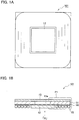
- Fig. 1A is a bottom view of a wireless power supply coil unit (hereinafter referred to as a "coil unit") according to a first embodiment helpful for understanding the present invention
- Fig. 1B is a lateral cross-sectional view of the coil unit.
- Fig. 1A is a view as viewed in the direction indicated by arrow A in Fig. 1B .
- the coil unit is a power receiving coil unit installed on the base of a vehicle to receive power transmitted from the ground side.
- the coil unit 101 includes a flat base plate 13 made of aluminum and fixed to the base of the vehicle.
- the coil unit 101 further includes a first ferrite 11 (a first magnetic body) having a plate shape and arranged on the bottom side of the base plate 13, and a second ferrite 12 (a second magnetic body) having a plate shape and arranged on the bottom side (on one side) of the first ferrite 11.
- the first ferrite 11 is provided with a rectangular opening 11a in the center, and the second ferrite 12 is located at a position corresponding to the opening 11a.
- a flat insulating plate 14 including insulating material such as plastic or resin is arranged between the first ferrite 11 and the second ferrite 12.
- a coil 15 with wound litz wire (electrical wire) is placed at the periphery of the first ferrite 11 on the bottom side.
- the coil 15 has a coil axis in the vertical direction, and has a hole in the center. The position at which the second ferrite 12 is arranged corresponds to the hole of the coil 15.
- the coil 15 is connected to a capacitor (not shown) to implement a resonance circuit for receiving power.
- the coil unit 101 is fabricated such that the base plate 13, the first ferrite 11, the insulating plate 14, and the second ferrite 12 are sequentially arranged, and the coil 15 is further placed thereon so as to be filled with resin around the entire circumference to be fixed together.
- the coil unit 101 is positioned to face a power transmitting coil (not shown) placed on the ground side, so that magnetic flux, which is output from the power transmitting coil upon excitation, links with the coil in the coil unit 101, thus receiving the power wirelessly.
- the second ferrite 12 has a slightly larger size than the opening 11a provided in the center of the first ferrite 11.
- the second ferrite 12 is arranged such that the center conforms to the center of the opening 11a of the second ferrite 12, so that the periphery of the second ferrite 12 overlaps with the circumferential part around the opening 11a.
- the overlapping part is illustrated in Fig. 1B as indicated by reference sign P1.
- an overlapping width YOL between the first ferrite 11 and the second ferrite 12 is set to be greater than or equal to a plate thickness TFe of the first ferrite 11, as given by YOL ⁇ TFe.
- the overlapping part between the first ferrite 11 and the second ferrite 12 provides a magnetic flux path equivalent to the first ferrite 11 having the plate thickness TFe, so as to allow the magnetic flux to flow through, as illustrated in Fig. 2B .
- a magnetic flux density in the first ferrite 11 thus can be substantially equalized with that in the overlapping part. This can avoid a concentration of the magnetic flux to prevent heat generation accordingly.
- the present embodiment fulfills the relationship as given by YOL ⁇ TFe so as to avoid such a problem.
- the insulating plate 14 may cause dielectric breakdown to lead a corona discharge to occur if a voltage applied between the first ferrite 11 and the second ferrite 12 increases.
- the applied voltage VLmax is the maximum voltage between the first ferrite 11 and the second ferrite 12. Setting the plate thickness Tb of the insulating plate 14 to greater than or equal to the minimum plate thickness Tb0 as represented by the formula (1) when the applied voltage is VLmax, can avoid the occurrence of the corona discharge.
- a minimum overlapping width YOLmin is equal to the thickness TFe of the first ferrite 11, since the relationship as given by YOL ⁇ TFe is fulfilled, as described above.
- the overlapping width YOL can be set to fulfill the following formula (5): YOL ⁇ Tb / Tb 0 ⁇ TFe
- the overlapping width YOL between the first ferrite 11 and the second ferrite 12 is determined in accordance with the plate thickness TFe of the first ferrite 11 and the plate thickness Tb of the insulating plate 14.
- the above maximum voltage VLmax can be a voltage applied to the coil.
- the voltage applied to the coil is 1.5 kV, which is set as the maximum voltage VLmax.
- the threshold of the corona discharge is set to three (kV/mm)
- the overlapping width YOL thus can be calculated by substituting, in the formula (5), 0.5 for Tb0, the actual plate thickness of the insulating plate 14 for Tb, and the actual plate thickness of the first ferrite 11 for TFe.
- the operational effects of the coil unit 101 according to the present embodiment are described below.
- the coil unit 101 configured as described above is positioned to face a power transmitting coil unit on the ground side, so that the magnetic flux generated by the power transmitting coil unit links with the coil unit 101.
- the magnetic flux then flows through the overlapping part.
- the overlapping width YOL set to greater than or equal to the plate thickness TFe of the first ferrite 11 can avoid an increase in the magnetic flux density to prevent heat generation.
- the first ferrite 11 and the second ferrite 12 are arranged with the insulating plate 14 interposed therebetween so as not to be in direct contact with each other. This also prevents heat generation due to a concentration of the magnetic field.
- the coil unit 101 includes the first ferrite 11 and the second ferrite 12, which is arranged on one side of the first ferrite 11 at the position corresponding to the opening 11a, and further includes the insulating plate 14 including insulating material such as resin and interposed between the first ferrite 11 and the second ferrite 12. Avoiding direct contact between the first ferrite 11 and the second ferrite 12 can prevent or reduce the dielectric breakdown at the contact surfaces between the first ferrite 11 and the second ferrite 12. Further, avoiding the use of the entirely-integrated ferrite structure, as described in the conventional case, increases the surface stiffness of each ferrite.
- the arrangement of the second ferrite 12 partly overlapping with the first ferrite 11 allows the magnetic flux to flow through the overlapping part, so as to improve the efficiency of transmitting and receiving power.
- the overlapping width YOL between the first ferrite 11 and the second ferrite 12 which is set to greater than or equal to the plate thickness TFe of the first ferrite 11, enables the density of the magnetic flux flowing through the first ferrite 11 to be substantially equivalent to that of the magnetic flux flowing through the overlapping part, avoiding the problem of causing heat generation to decrease the power supply efficiency accordingly.
- the overlapping width YOL between the first ferrite 11 and the second ferrite 12 is set to increase as the plate thickness Tb of the insulating plate 14 increases, as indicated by the formula (5), so as to allow the magnetic flux to flow through more efficiently.
- the present invention is not intended to be limited to this case, and may be applied to a power transmitting coil unit placed on the ground side.
- the arrangement direction of the coil unit illustrated in the first embodiment is vertically inverted.
- Fig. 4 is a partial cross-sectional view of a coil unit 102 according to the second embodiment.
- the second embodiment uses litz wire, composing the coil 15 wound around the second ferrite 12, provided with a covering 22.
- the insulating plate 14 is not placed on the first ferrite 11 on the outside of the second ferrite 12. As illustrated in Fig. 4 , the insulating plate 14 is arranged only on the upper surface of the second ferrite 12.
- Such arrangement also enables the coil 15 to be insulated without the insulating plate 14 arranged in the region on which the coil 15 is wound, so as to achieve the effects similar to those of the above first embodiment.
- This arrangement is advantageous to the case of using the covered litz wire to compose the coil 15.
- Fig. 5 is a partial cross-sectional view of a coil unit 103 according to the third embodiment.
- the third embodiment differs from the above first embodiment in eliminating the arrangement of the insulating plate 14 at a position corresponding to the hollow of the first ferrite 11.
- the insulating plate 14 is arranged only in the region at which the first ferrite 11 overlaps with the second ferrite 12 and in the region on the first ferrite 11 on which the coil 15 is wound, while the insulating plate 14 is not arranged at a position corresponding to the opening 11a.
- This structure decreases the arrangement area of the insulating plate 14, reducing the amount of the material used accordingly.
- FIG. 6 is a partial cross-sectional view of a coil unit 104 according to the fourth embodiment.
- the coil unit 104 according to the fourth embodiment includes an insulating plate 14a provided with grooves 21 having an arc shape in cross section in a region on which the coil 15 is wound.
- the grooves 21 for winding the coil 15 are formed on the insulating plate 14a arranged on the surface of the magnetic body (the first ferrite 11).
- the coil 15 is placed to fit in the grooves 21.
- the insulating plate 14a provided with the grooves 21 for coil winding thus serves as a bobbin for holding the coil 15.
- the fourth embodiment having the above structure can also achieve the effects similar to those of the first embodiment.
- the insulating plate 14a also serving as a bobbin facilitates the process of winding the coil 15 on the surface of the first ferrite 11.
- the litz wire composing the coil 15 wound around the second ferrite 12 may be provided with the covering 22, and in an example that does not form part of the present invention, the first ferrite 11 may be provided on the surface with grooves so as to fit the coil 15 in the grooves. This structure allows the first ferrite 11 to also serve as a bobbin, so as to facilitate the process of winding the coil 15 on the surface of the first ferrite 11.
Landscapes
- Engineering & Computer Science (AREA)
- Power Engineering (AREA)
- Transportation (AREA)
- Mechanical Engineering (AREA)
- Computer Networks & Wireless Communication (AREA)
- Chemical & Material Sciences (AREA)
- Composite Materials (AREA)
- Current-Collector Devices For Electrically Propelled Vehicles (AREA)
- Electric Propulsion And Braking For Vehicles (AREA)
- Charge And Discharge Circuits For Batteries Or The Like (AREA)
- Coils Of Transformers For General Uses (AREA)
Description
- The present invention relates to a wireless power supply coil unit used for wirelessly charging a battery mounted on a vehicle.
- A wireless power supply coil unit mounted on a vehicle preferably has a structure having a hollow projection in cross section in the middle which is a space for installing a capacitor so as to reduce the entire thickness. Patent Document 1 discloses a wireless power supply coil unit of this type. The coil unit disclosed in Patent Document 1 is used for a mobile phone to supply power wirelessly, and includes a ferrite material (a magnetic body) used for a coil and having a projection in cross section in the middle on which wire is wound. A ferrite material, if used in a wireless power supply coil unit for a vehicle, inevitably has a larger size than that for a mobile phone, and can have less surface stiffness when having a projection in cross section.
- Patent Document 2 discloses a coil unit including a plurality of flat ferrite materials brought in surface contact to partly overlap with each other so as to entirely define a projection in cross section. However, the surface contact between the ferrite materials may cause dielectric breakdown across a gap if the surfaces in contact with each other would be partly separated.
-
- Patent Document 1:
Japanese Unexamined Patent Application Publication No. 2008-294385 - Patent Document 2:
Japanese Unexamined Patent Application Publication No. 2015-106939 - Further than that, European patent application
EP2535906A1 discloses a non-contact charging device that comprises a power receiving device, wherein the power receiving device comprises a wound coil and a first and a second magnetic body. - As described above, the magnetic body (the ferrite material) having a projection used for a wireless power supply coil unit mounted on a vehicle has a problem of being damaged by external stress. In addition, the use of the plural ferrite materials brought in surface contact to provide a projection has a problem of causing dielectric breakdown between the surfaces of the ferrite materials in contact with each other.
- To solve the conventional problems described above, the present invention provides a wireless power supply coil unit having high surface stiffness of ferrites and avoiding dielectric breakdown between contact surfaces of the ferrites.
- A first aspect of the present invention provides a wireless power supply coil unit according to claims 1 and 2.
- The coil unit according to the first aspect of the present invention has high surface stiffness of ferrites and prevents or reduces dielectric breakdown between contact surfaces of the ferrites
-
- [
Fig. 1A] Fig. 1A is a bottom view of a coil unit according to a first embodiment helpful for understanding the present invention. - [
Fig. 1B] Fig. 1B is a lateral cross-sectional view of the coil unit according to the first embodiment. - [
Fig. 2A] Fig. 2A is a view illustrating an overlapping part between a first ferrite and a second ferrite. - [
Fig. 2B] Fig. 2B is a view illustrating magnetic flux flowing through the overlapping part between the first ferrite and the second ferrite, showing a state in which an overlapping width is greater than or equal to a plate thickness of the first ferrite. - [
Fig. 2C] Fig. 2C is a view illustrating magnetic flux flowing through the overlapping part between the first ferrite and the second ferrite, showing a state in which the overlapping width is less than the plate thickness of the first ferrite. - [
Fig. 3] Fig. 3 is a view illustrating a voltage applied to an insulating plate. - [
Fig. 4] Fig. 4 is a view illustrating an overlapping part between a first ferrite and a second ferrite of a coil unit according to a second embodiment helpful for understanding the present invention. - [
Fig. 5] Fig. 5 is a view illustrating an overlapping part between a first ferrite and a second ferrite of a coil unit according to a third embodiment helpful for understanding the present invention - [
Fig. 6] Fig. 6 is a view illustrating an overlapping part between a first ferrite and a second ferrite of a coil unit according to a fourth embodiment, which is an embodiment of the present invention - Hereinafter, embodiments according to the present invention will be described with reference to the fourth embodiment and to
figure 6 . The remaining first, second and third embodiments and the accompanyingfigures 1A, 1B ,2A, 2B ,2C ,3 ,4 and5 constitute examples useful for the understanding the principles of the present invention and do not form part of the present invention. -
Fig. 1A is a bottom view of a wireless power supply coil unit (hereinafter referred to as a "coil unit") according to a first embodiment helpful for understanding the present invention, andFig. 1B is a lateral cross-sectional view of the coil unit.Fig. 1A is a view as viewed in the direction indicated by arrow A inFig. 1B . The coil unit is a power receiving coil unit installed on the base of a vehicle to receive power transmitted from the ground side. - As shown in
Fig. 1A and Fig. 1B , thecoil unit 101 includes aflat base plate 13 made of aluminum and fixed to the base of the vehicle. Thecoil unit 101 further includes a first ferrite 11 (a first magnetic body) having a plate shape and arranged on the bottom side of thebase plate 13, and a second ferrite 12 (a second magnetic body) having a plate shape and arranged on the bottom side (on one side) of thefirst ferrite 11. - The
first ferrite 11 is provided with arectangular opening 11a in the center, and thesecond ferrite 12 is located at a position corresponding to the opening 11a. - A flat
insulating plate 14 including insulating material such as plastic or resin is arranged between thefirst ferrite 11 and thesecond ferrite 12. Acoil 15 with wound litz wire (electrical wire) is placed at the periphery of thefirst ferrite 11 on the bottom side. Thecoil 15 has a coil axis in the vertical direction, and has a hole in the center. The position at which thesecond ferrite 12 is arranged corresponds to the hole of thecoil 15. Thecoil 15 is connected to a capacitor (not shown) to implement a resonance circuit for receiving power. - The
coil unit 101 is fabricated such that thebase plate 13, thefirst ferrite 11, theinsulating plate 14, and thesecond ferrite 12 are sequentially arranged, and thecoil 15 is further placed thereon so as to be filled with resin around the entire circumference to be fixed together. Thecoil unit 101 is positioned to face a power transmitting coil (not shown) placed on the ground side, so that magnetic flux, which is output from the power transmitting coil upon excitation, links with the coil in thecoil unit 101, thus receiving the power wirelessly. - A positional relationship between the
first ferrite 11 and thesecond ferrite 12 is described below. Thesecond ferrite 12 has a slightly larger size than theopening 11a provided in the center of thefirst ferrite 11. Thesecond ferrite 12 is arranged such that the center conforms to the center of theopening 11a of thesecond ferrite 12, so that the periphery of thesecond ferrite 12 overlaps with the circumferential part around theopening 11a. The overlapping part is illustrated inFig. 1B as indicated by reference sign P1. - According to the present embodiment, as illustrated in
Fig. 2A , an overlapping width YOL between thefirst ferrite 11 and thesecond ferrite 12 is set to be greater than or equal to a plate thickness TFe of thefirst ferrite 11, as given by YOL ≥ TFe. The overlapping part between thefirst ferrite 11 and thesecond ferrite 12 provides a magnetic flux path equivalent to thefirst ferrite 11 having the plate thickness TFe, so as to allow the magnetic flux to flow through, as illustrated inFig. 2B . A magnetic flux density in thefirst ferrite 11 thus can be substantially equalized with that in the overlapping part. This can avoid a concentration of the magnetic flux to prevent heat generation accordingly. - If the relationship as given by YOL ≥ TFe is not fulfilled, the magnetic flux density in the overlapping part PI increases, as illustrated in
Fig. 2C , causing heat generation to increase a loss. The present embodiment fulfills the relationship as given by YOL ≥ TFe so as to avoid such a problem. - A relationship between the overlapping width YOL, a plate thickness of the insulating
plate 14 as indicated by sign Tb, and the plate thickness TFe of thefirst ferrite 11, as shown inFig. 2A , is described below. The insulatingplate 14 may cause dielectric breakdown to lead a corona discharge to occur if a voltage applied between thefirst ferrite 11 and thesecond ferrite 12 increases. A minimum plate thickness Tb0 sufficient to prevent the corona discharge can be represented by the following formula (1):
first ferrite 11 and thesecond ferrite 12. Setting the plate thickness Tb of the insulatingplate 14 to greater than or equal to the minimum plate thickness Tb0 as represented by the formula (1) when the applied voltage is VLmax, can avoid the occurrence of the corona discharge. - A minimum overlapping width YOLmin is equal to the thickness TFe of the
first ferrite 11, since the relationship as given by YOL ≥ TFe is fulfilled, as described above. The minimum overlapping width YOLmin is thus represented by the following formula (2):
- A minimum magnetic resistance Rm_min of the overlapping part, which is a magnetic resistance when the overlapping part has the minimum overlapping width YOLmin (= TFe), is represented by the following formula (3):

first ferrite 11 and thesecond ferrite 12, which is the plate thickness of the insulatingplate 14, µ is magnetic permeability, S is an area of the overlapping part, and X is a length of the overlapping part in depth in the horizontal direction. - For the use of the insulating
plate 14 having an optional plate thickness Tb, the magnetic resistance Rm can be represented by the following formula (4):
- To achieve the minimum magnetic resistance or less using the insulating
plate 14 having an optional plate thickness Tb according to the formulae (3) and (4), the overlapping width YOL can be set to fulfill the following formula (5):
- The overlapping width YOL between the
first ferrite 11 and thesecond ferrite 12 is determined in accordance with the plate thickness TFe of thefirst ferrite 11 and the plate thickness Tb of the insulatingplate 14. - The above maximum voltage VLmax can be a voltage applied to the coil. For example, as illustrated in
Fig. 3 , the voltage applied to the coil is 1.5 kV, which is set as the maximum voltage VLmax. When the threshold of the corona discharge is set to three (kV/mm), for example, the minimum plate thickness Tb0 of the insulatingplate 14 results in Tb0 = 0.5 mm in accordance with the formula (1). The overlapping width YOL thus can be calculated by substituting, in the formula (5), 0.5 for Tb0, the actual plate thickness of the insulatingplate 14 for Tb, and the actual plate thickness of thefirst ferrite 11 for TFe. - The operational effects of the
coil unit 101 according to the present embodiment are described below. Thecoil unit 101 configured as described above is positioned to face a power transmitting coil unit on the ground side, so that the magnetic flux generated by the power transmitting coil unit links with thecoil unit 101. The magnetic flux then flows through the overlapping part. The overlapping width YOL set to greater than or equal to the plate thickness TFe of thefirst ferrite 11 can avoid an increase in the magnetic flux density to prevent heat generation. Thefirst ferrite 11 and thesecond ferrite 12 are arranged with the insulatingplate 14 interposed therebetween so as not to be in direct contact with each other. This also prevents heat generation due to a concentration of the magnetic field. - Setting the plate thickness Tb of the insulating
plate 14 to fulfill the formula (5) can prevent dielectric breakdown of the insulatingplate 14 to avoid occurrence of a corona discharge. - The
coil unit 101 according to the first embodiment includes thefirst ferrite 11 and thesecond ferrite 12, which is arranged on one side of thefirst ferrite 11 at the position corresponding to theopening 11a, and further includes the insulatingplate 14 including insulating material such as resin and interposed between thefirst ferrite 11 and thesecond ferrite 12. Avoiding direct contact between thefirst ferrite 11 and thesecond ferrite 12 can prevent or reduce the dielectric breakdown at the contact surfaces between thefirst ferrite 11 and thesecond ferrite 12. Further, avoiding the use of the entirely-integrated ferrite structure, as described in the conventional case, increases the surface stiffness of each ferrite. - The arrangement of the
second ferrite 12 partly overlapping with thefirst ferrite 11 allows the magnetic flux to flow through the overlapping part, so as to improve the efficiency of transmitting and receiving power. - The overlapping width YOL between the
first ferrite 11 and thesecond ferrite 12 which is set to greater than or equal to the plate thickness TFe of thefirst ferrite 11, enables the density of the magnetic flux flowing through thefirst ferrite 11 to be substantially equivalent to that of the magnetic flux flowing through the overlapping part, avoiding the problem of causing heat generation to decrease the power supply efficiency accordingly. - The overlapping width YOL between the
first ferrite 11 and thesecond ferrite 12 is set to increase as the plate thickness Tb of the insulatingplate 14 increases, as indicated by the formula (5), so as to allow the magnetic flux to flow through more efficiently. - While the above embodiment has been illustrated with the case of the power receiving coil unit mounted on the base of a vehicle, the present invention is not intended to be limited to this case, and may be applied to a power transmitting coil unit placed on the ground side. In such a case, the arrangement direction of the coil unit illustrated in the first embodiment is vertically inverted.
- A second embodiment helpful for understanding the present invention is described below.
Fig. 4 is a partial cross-sectional view of acoil unit 102 according to the second embodiment. The second embodiment uses litz wire, composing thecoil 15 wound around thesecond ferrite 12, provided with acovering 22. The insulatingplate 14 is not placed on thefirst ferrite 11 on the outside of thesecond ferrite 12. As illustrated inFig. 4 , the insulatingplate 14 is arranged only on the upper surface of thesecond ferrite 12. - Such arrangement also enables the
coil 15 to be insulated without the insulatingplate 14 arranged in the region on which thecoil 15 is wound, so as to achieve the effects similar to those of the above first embodiment. This arrangement is advantageous to the case of using the covered litz wire to compose thecoil 15. - A third embodiment helpful for understanding the present invention is described below.
Fig. 5 is a partial cross-sectional view of acoil unit 103 according to the third embodiment. The third embodiment differs from the above first embodiment in eliminating the arrangement of the insulatingplate 14 at a position corresponding to the hollow of thefirst ferrite 11. In particular, the insulatingplate 14 is arranged only in the region at which thefirst ferrite 11 overlaps with thesecond ferrite 12 and in the region on thefirst ferrite 11 on which thecoil 15 is wound, while the insulatingplate 14 is not arranged at a position corresponding to theopening 11a. This structure decreases the arrangement area of the insulatingplate 14, reducing the amount of the material used accordingly. - A fourth embodiment, which is an embodiment according to the present invention, is described below.
Fig. 6 is a partial cross-sectional view of acoil unit 104 according to the fourth embodiment. Thecoil unit 104 according to the fourth embodiment includes an insulatingplate 14a provided withgrooves 21 having an arc shape in cross section in a region on which thecoil 15 is wound. Thegrooves 21 for winding thecoil 15 are formed on the insulatingplate 14a arranged on the surface of the magnetic body (the first ferrite 11). Thecoil 15 is placed to fit in thegrooves 21. The insulatingplate 14a provided with thegrooves 21 for coil winding thus serves as a bobbin for holding thecoil 15. - The fourth embodiment having the above structure can also achieve the effects similar to those of the first embodiment. The insulating
plate 14a also serving as a bobbin facilitates the process of winding thecoil 15 on the surface of thefirst ferrite 11. - The litz wire composing the
coil 15 wound around thesecond ferrite 12 may be provided with the covering 22, and in an example that does not form part of the present invention, thefirst ferrite 11 may be provided on the surface with grooves so as to fit thecoil 15 in the grooves. This structure allows thefirst ferrite 11 to also serve as a bobbin, so as to facilitate the process of winding thecoil 15 on the surface of thefirst ferrite 11. - While the wireless power supply coil unit according to the present invention has been described above by reference to the respective embodiments as illustrated in the drawings, it should be understood that the present invention is only limited by the claims.
-
- 11
- FIRST FERRITE (FIRST MAGNETIC BODY)
- 11a
- OPENING
- 12
- SECOND FERRITE (SECOND MAGNETIC BODY)
- 13
- BASEPLATE
- 14
- INSULATING PLATE
- 15
- COIL
- 21
- GROOVE
- 22
- COVERING
- 101, 102, 103, 104
- COIL UNIT
Claims (3)
- A wireless power supply coil unit (104) for receiving power wirelessly when mounted on the base of a vehicle, the wireless power supply coil unit (104) comprising:a first magnetic body with a plate-like shape having a surface and a thickness;a coil (15) having a hollow portion in a center of the coil (15) and a coil axis which extends along the thickness of the first magnetic body, wherein the coil has an electric wire wound horizontally relative to the coil axis, the first magnetic body (11) having an opening (11a) at a position corresponding to the hollow portion in the center of the coil (15), the center of the opening (11a) corresponding to the coil axis;a second magnetic body (12) having a plate-like shape and arranged in the hollow portion in the center of the coil (15) on a bottom side of the first magnetic body (11) and whose center corresponds to the coil axis, and a periphery of the second magnetic body (12) overlaps with a circumferential part around the opening (11a) of the first magnetic body (11); andan insulating plate (14) interposed between the bottom side of the first magnetic body (11) and a top side of the second magnetic body (12),wherein an overlapping width YOL between the first magnetic body (11) and the second magnetic body (12) is greater than or equal to the thickness of the first magnetic body (11), andcharacterized in thatthe insulating plate (14) is provided with a groove for coil winding, and wherein the coil (15) is placed to fit in the groove (21).
- A wireless power supply coil unit (104) for transmitting power wirelessly when placed on a ground side, the wireless power supply coil unit (104) comprising:a first magnetic body with a plate-like shape having a surface and a thickness;a coil (15) having a hollow portion in a center of the coil (15) and a coil axis which extends along the thickness of the first magnetic body, wherein the coil has an electric wire wound horizontally relative to the coil axis, the first magnetic body (11) having an opening (11a) at a position corresponding to the hollow portion in the center of the coil (15), the center of the opening (11a) corresponding to the coil axis;a second magnetic body (12) having a plate-like shape and arranged in the hollow portion in the center of the coil (15) on a top side of the first magnetic body (11) and whose center corresponds to the coil axis, and a periphery of the second magnetic body (12) overlaps with a circumferential part around the opening (11a) of the first magnetic body (11); andan insulating plate (14) interposed between the top side of the first magnetic body (11) and a bottom side of the second magnetic body (12),wherein an overlapping width YOL between the first magnetic body (11) and the second magnetic body (12) is greater than or equal to the thickness of the first magnetic body (11), andcharacterized in thatthe insulating plate (14) is provided with a groove for coil winding, and wherein the coil (15) is placed to fit in the groove (21).
- The wireless power supply coil unit (104) according to claim 1 or 2, wherein the
overlapping width YOL between the first magnetic body (11) and the second magnetic body (12) is set to fulfill the following formula:
a minimum plate thickness Tb0 of the insulating plate (14) is calculated according to the following formula:
a plate thickness of the insulating plate (14) is set to be greater than or equal to the minimum plate thickness Tb0.
Applications Claiming Priority (1)
| Application Number | Priority Date | Filing Date | Title |
|---|---|---|---|
| PCT/JP2017/003150 WO2018138909A1 (en) | 2017-01-30 | 2017-01-30 | Non-contact power supply coil unit |
Publications (3)
| Publication Number | Publication Date |
|---|---|
| EP3576117A1 EP3576117A1 (en) | 2019-12-04 |
| EP3576117A4 EP3576117A4 (en) | 2020-01-01 |
| EP3576117B1 true EP3576117B1 (en) | 2021-12-29 |
Family
ID=62979221
Family Applications (1)
| Application Number | Title | Priority Date | Filing Date |
|---|---|---|---|
| EP17893890.8A Active EP3576117B1 (en) | 2017-01-30 | 2017-01-30 | Non-contact power supply coil unit |
Country Status (9)
| Country | Link |
|---|---|
| US (1) | US10796848B2 (en) |
| EP (1) | EP3576117B1 (en) |
| JP (1) | JP6702440B2 (en) |
| KR (1) | KR102152919B1 (en) |
| CN (1) | CN110235214B (en) |
| CA (1) | CA3051820C (en) |
| MX (1) | MX388807B (en) |
| RU (1) | RU2713386C1 (en) |
| WO (1) | WO2018138909A1 (en) |
Families Citing this family (2)
| Publication number | Priority date | Publication date | Assignee | Title |
|---|---|---|---|---|
| KR102292033B1 (en) * | 2020-11-26 | 2021-08-20 | (주)플렉스파워 | Pad integrated wireless charging device |
| JP7794111B2 (en) * | 2022-12-07 | 2026-01-06 | トヨタ自動車株式会社 | Power receiving device and wireless power supply system |
Family Cites Families (23)
| Publication number | Priority date | Publication date | Assignee | Title |
|---|---|---|---|---|
| JPS63113913A (en) * | 1986-10-31 | 1988-05-18 | Nec Corp | Magnetoresistance effect type thin film magnetic head and its production |
| JPH035965A (en) * | 1989-06-01 | 1991-01-11 | Pioneer Electron Corp | Data recording method |
| WO1996042096A1 (en) * | 1995-06-09 | 1996-12-27 | Matsushita Electric Industrial Co., Ltd. | Reactor and method of production thereof |
| JPH0935965A (en) * | 1995-07-18 | 1997-02-07 | Matsushita Electric Ind Co Ltd | Reactor |
| JPH095965A (en) * | 1995-06-20 | 1997-01-10 | Fuji Photo Film Co Ltd | Method for processing silver halide color photographic sensitive material |
| DE10312284B4 (en) * | 2003-03-19 | 2005-12-22 | Sew-Eurodrive Gmbh & Co. Kg | Transducer head, system for contactless energy transmission and use of a transmitter head |
| JP4776185B2 (en) * | 2004-07-14 | 2011-09-21 | Tdk株式会社 | Coil parts |
| JP2007285774A (en) | 2006-04-13 | 2007-11-01 | Toyota Motor Corp | Magnetic resolver and manufacturing method thereof |
| JP4209437B2 (en) | 2006-11-10 | 2009-01-14 | 三菱重工業株式会社 | Non-contact power feeding device for mobile body and protection device therefor |
| JP2008294385A (en) | 2007-04-24 | 2008-12-04 | Panasonic Electric Works Co Ltd | Non-contact power transmission device and method for manufacturing coil block for receiving power |
| JP5118394B2 (en) | 2007-06-20 | 2013-01-16 | パナソニック株式会社 | Non-contact power transmission equipment |
| GB0716679D0 (en) * | 2007-08-28 | 2007-10-03 | Fells J | Inductive power supply |
| JP2010041906A (en) | 2008-07-10 | 2010-02-18 | Nec Tokin Corp | Contactless power transmission apparatus, soft magnetic sheet, and module using the same |
| US9143041B2 (en) * | 2010-02-05 | 2015-09-22 | Hitachi Metals, Ltd. | Magnetic circuit, power-supplying device and power-receiving device for non-contact charging apparatus, and non-contact charging apparatus |
| JP6034644B2 (en) | 2012-10-10 | 2016-11-30 | デクセリアルズ株式会社 | Composite coil module and portable device |
| JP6164421B2 (en) | 2013-11-28 | 2017-07-19 | Tdk株式会社 | Power transmission coil unit and wireless power transmission device |
| JP6217435B2 (en) * | 2014-02-13 | 2017-10-25 | トヨタ自動車株式会社 | Power receiving device |
| JP6434763B2 (en) * | 2014-09-29 | 2018-12-05 | ルネサスエレクトロニクス株式会社 | Semiconductor device |
| JP2016105435A (en) * | 2014-12-01 | 2016-06-09 | トヨタ自動車株式会社 | Power reception device and power transmission device |
| JP2016129164A (en) * | 2015-01-09 | 2016-07-14 | トヨタ自動車株式会社 | Power receiving device and power transmitting device |
| JP6172185B2 (en) * | 2015-03-11 | 2017-08-02 | トヨタ自動車株式会社 | Power receiving device and power transmitting device |
| JP6580387B2 (en) * | 2015-06-19 | 2019-09-25 | 矢崎総業株式会社 | Coil unit |
| JP2017017874A (en) | 2015-07-01 | 2017-01-19 | 株式会社Ihi | Coil device |
-
2017
- 2017-01-30 MX MX2019008838A patent/MX388807B/en unknown
- 2017-01-30 JP JP2018564073A patent/JP6702440B2/en active Active
- 2017-01-30 CN CN201780085080.7A patent/CN110235214B/en active Active
- 2017-01-30 WO PCT/JP2017/003150 patent/WO2018138909A1/en not_active Ceased
- 2017-01-30 KR KR1020197021752A patent/KR102152919B1/en not_active Expired - Fee Related
- 2017-01-30 EP EP17893890.8A patent/EP3576117B1/en active Active
- 2017-01-30 US US16/478,957 patent/US10796848B2/en active Active
- 2017-01-30 CA CA3051820A patent/CA3051820C/en active Active
- 2017-01-30 RU RU2019127041A patent/RU2713386C1/en active
Non-Patent Citations (1)
| Title |
|---|
| None * |
Also Published As
| Publication number | Publication date |
|---|---|
| US20190348218A1 (en) | 2019-11-14 |
| MX2019008838A (en) | 2019-09-10 |
| JPWO2018138909A1 (en) | 2019-11-21 |
| KR102152919B1 (en) | 2020-09-07 |
| CA3051820A1 (en) | 2018-08-02 |
| JP6702440B2 (en) | 2020-06-03 |
| WO2018138909A1 (en) | 2018-08-02 |
| CA3051820C (en) | 2020-02-25 |
| EP3576117A1 (en) | 2019-12-04 |
| KR20190103235A (en) | 2019-09-04 |
| US10796848B2 (en) | 2020-10-06 |
| MX388807B (en) | 2025-03-20 |
| CN110235214A (en) | 2019-09-13 |
| EP3576117A4 (en) | 2020-01-01 |
| RU2713386C1 (en) | 2020-02-05 |
| CN110235214B (en) | 2020-08-21 |
Similar Documents
| Publication | Publication Date | Title |
|---|---|---|
| US10404102B2 (en) | Power feeding coil unit, wireless power feeding device and wireless power transmission device | |
| US20180175670A1 (en) | Non-contact charging module having a wireless charging coil and a magnetic sheet | |
| EP2586044B1 (en) | Coil and electric shielding arrangement, transformer comprising the arrangement and a method of manufacturing the arrangement. | |
| WO2012039245A1 (en) | Coil module for contactless electric power transfer, and battery pack and charging device provided with same | |
| US9667089B2 (en) | Secondary coil module | |
| US20170063155A1 (en) | Power Supply Device | |
| JP2012023090A (en) | Reactor | |
| EP2660833B1 (en) | Ignition coil | |
| EP3576117A1 (en) | Non-contact power supply coil unit | |
| KR100978503B1 (en) | Slim type high voltage transformer | |
| JP4900525B1 (en) | Non-contact charging module, transmitting-side non-contact charging device and receiving-side non-contact charging device provided with the same | |
| JP4962634B1 (en) | Method for manufacturing contactless charging module | |
| JP5216490B2 (en) | Outer iron type amorphous transformer | |
| US20220044868A1 (en) | Wireless power transfer coupling structures with reduced leakage flux | |
| JP2012023079A (en) | Reactor | |
| US20170274779A1 (en) | Wireless power supply apparatus | |
| US12140611B2 (en) | Protection of an AC device | |
| JP4291422B2 (en) | Ignition coil for internal combustion engine | |
| EP3054464B1 (en) | Coupling coil structure and transformer | |
| JP5824631B2 (en) | Non-contact charging module and charger and electronic device using the same | |
| US20250014810A1 (en) | Wireless power-charging module and method for assembling that same | |
| JP2004071917A (en) | Ignition coil for internal combustion engine | |
| JPH07254519A (en) | Stationary induction |
Legal Events
| Date | Code | Title | Description |
|---|---|---|---|
| STAA | Information on the status of an ep patent application or granted ep patent |
Free format text: STATUS: THE INTERNATIONAL PUBLICATION HAS BEEN MADE |
|
| PUAI | Public reference made under article 153(3) epc to a published international application that has entered the european phase |
Free format text: ORIGINAL CODE: 0009012 |
|
| STAA | Information on the status of an ep patent application or granted ep patent |
Free format text: STATUS: REQUEST FOR EXAMINATION WAS MADE |
|
| 17P | Request for examination filed |
Effective date: 20190805 |
|
| AK | Designated contracting states |
Kind code of ref document: A1 Designated state(s): AL AT BE BG CH CY CZ DE DK EE ES FI FR GB GR HR HU IE IS IT LI LT LU LV MC MK MT NL NO PL PT RO RS SE SI SK SM TR |
|
| AX | Request for extension of the european patent |
Extension state: BA ME |
|
| RIC1 | Information provided on ipc code assigned before grant |
Ipc: H01F 38/14 20060101AFI20191106BHEP Ipc: H01F 27/30 20060101ALI20191106BHEP Ipc: H02J 50/12 20160101ALI20191106BHEP Ipc: H02J 50/10 20160101ALI20191106BHEP Ipc: H02J 7/00 20060101ALI20191106BHEP Ipc: H01F 3/10 20060101ALI20191106BHEP Ipc: H01F 27/36 20060101ALI20191106BHEP Ipc: B60L 53/12 20190101ALI20191106BHEP |
|
| A4 | Supplementary search report drawn up and despatched |
Effective date: 20191202 |
|
| RIC1 | Information provided on ipc code assigned before grant |
Ipc: H01F 38/14 20060101AFI20191122BHEP Ipc: H01F 27/30 20060101ALI20191122BHEP Ipc: H02J 50/10 20160101ALI20191122BHEP Ipc: H02J 7/00 20060101ALI20191122BHEP Ipc: H01F 3/10 20060101ALI20191122BHEP Ipc: H01F 27/36 20060101ALI20191122BHEP Ipc: H02J 50/12 20160101ALI20191122BHEP Ipc: B60L 53/12 20190101ALI20191122BHEP |
|
| DAV | Request for validation of the european patent (deleted) | ||
| DAX | Request for extension of the european patent (deleted) | ||
| STAA | Information on the status of an ep patent application or granted ep patent |
Free format text: STATUS: EXAMINATION IS IN PROGRESS |
|
| 17Q | First examination report despatched |
Effective date: 20200805 |
|
| GRAP | Despatch of communication of intention to grant a patent |
Free format text: ORIGINAL CODE: EPIDOSNIGR1 |
|
| STAA | Information on the status of an ep patent application or granted ep patent |
Free format text: STATUS: GRANT OF PATENT IS INTENDED |
|
| INTG | Intention to grant announced |
Effective date: 20211021 |
|
| RIN1 | Information on inventor provided before grant (corrected) |
Inventor name: YAMAUCHI, YUUYA |
|
| GRAS | Grant fee paid |
Free format text: ORIGINAL CODE: EPIDOSNIGR3 |
|
| GRAA | (expected) grant |
Free format text: ORIGINAL CODE: 0009210 |
|
| STAA | Information on the status of an ep patent application or granted ep patent |
Free format text: STATUS: THE PATENT HAS BEEN GRANTED |
|
| AK | Designated contracting states |
Kind code of ref document: B1 Designated state(s): AL AT BE BG CH CY CZ DE DK EE ES FI FR GB GR HR HU IE IS IT LI LT LU LV MC MK MT NL NO PL PT RO RS SE SI SK SM TR |
|
| REG | Reference to a national code |
Ref country code: GB Ref legal event code: FG4D |
|
| REG | Reference to a national code |
Ref country code: CH Ref legal event code: EP |
|
| REG | Reference to a national code |
Ref country code: AT Ref legal event code: REF Ref document number: 1459307 Country of ref document: AT Kind code of ref document: T Effective date: 20220115 |
|
| REG | Reference to a national code |
Ref country code: IE Ref legal event code: FG4D |
|
| REG | Reference to a national code |
Ref country code: DE Ref legal event code: R096 Ref document number: 602017051722 Country of ref document: DE |
|
| REG | Reference to a national code |
Ref country code: LT Ref legal event code: MG9D |
|
| PG25 | Lapsed in a contracting state [announced via postgrant information from national office to epo] |
Ref country code: RS Free format text: LAPSE BECAUSE OF FAILURE TO SUBMIT A TRANSLATION OF THE DESCRIPTION OR TO PAY THE FEE WITHIN THE PRESCRIBED TIME-LIMIT Effective date: 20211229 Ref country code: LT Free format text: LAPSE BECAUSE OF FAILURE TO SUBMIT A TRANSLATION OF THE DESCRIPTION OR TO PAY THE FEE WITHIN THE PRESCRIBED TIME-LIMIT Effective date: 20211229 Ref country code: FI Free format text: LAPSE BECAUSE OF FAILURE TO SUBMIT A TRANSLATION OF THE DESCRIPTION OR TO PAY THE FEE WITHIN THE PRESCRIBED TIME-LIMIT Effective date: 20211229 Ref country code: BG Free format text: LAPSE BECAUSE OF FAILURE TO SUBMIT A TRANSLATION OF THE DESCRIPTION OR TO PAY THE FEE WITHIN THE PRESCRIBED TIME-LIMIT Effective date: 20220329 |
|
| REG | Reference to a national code |
Ref country code: NL Ref legal event code: MP Effective date: 20211229 |
|
| REG | Reference to a national code |
Ref country code: AT Ref legal event code: MK05 Ref document number: 1459307 Country of ref document: AT Kind code of ref document: T Effective date: 20211229 |
|
| PG25 | Lapsed in a contracting state [announced via postgrant information from national office to epo] |
Ref country code: SE Free format text: LAPSE BECAUSE OF FAILURE TO SUBMIT A TRANSLATION OF THE DESCRIPTION OR TO PAY THE FEE WITHIN THE PRESCRIBED TIME-LIMIT Effective date: 20211229 Ref country code: NO Free format text: LAPSE BECAUSE OF FAILURE TO SUBMIT A TRANSLATION OF THE DESCRIPTION OR TO PAY THE FEE WITHIN THE PRESCRIBED TIME-LIMIT Effective date: 20220329 Ref country code: LV Free format text: LAPSE BECAUSE OF FAILURE TO SUBMIT A TRANSLATION OF THE DESCRIPTION OR TO PAY THE FEE WITHIN THE PRESCRIBED TIME-LIMIT Effective date: 20211229 Ref country code: HR Free format text: LAPSE BECAUSE OF FAILURE TO SUBMIT A TRANSLATION OF THE DESCRIPTION OR TO PAY THE FEE WITHIN THE PRESCRIBED TIME-LIMIT Effective date: 20211229 Ref country code: GR Free format text: LAPSE BECAUSE OF FAILURE TO SUBMIT A TRANSLATION OF THE DESCRIPTION OR TO PAY THE FEE WITHIN THE PRESCRIBED TIME-LIMIT Effective date: 20220330 |
|
| PG25 | Lapsed in a contracting state [announced via postgrant information from national office to epo] |
Ref country code: NL Free format text: LAPSE BECAUSE OF FAILURE TO SUBMIT A TRANSLATION OF THE DESCRIPTION OR TO PAY THE FEE WITHIN THE PRESCRIBED TIME-LIMIT Effective date: 20211229 |
|
| PG25 | Lapsed in a contracting state [announced via postgrant information from national office to epo] |
Ref country code: SM Free format text: LAPSE BECAUSE OF FAILURE TO SUBMIT A TRANSLATION OF THE DESCRIPTION OR TO PAY THE FEE WITHIN THE PRESCRIBED TIME-LIMIT Effective date: 20211229 Ref country code: SK Free format text: LAPSE BECAUSE OF FAILURE TO SUBMIT A TRANSLATION OF THE DESCRIPTION OR TO PAY THE FEE WITHIN THE PRESCRIBED TIME-LIMIT Effective date: 20211229 Ref country code: RO Free format text: LAPSE BECAUSE OF FAILURE TO SUBMIT A TRANSLATION OF THE DESCRIPTION OR TO PAY THE FEE WITHIN THE PRESCRIBED TIME-LIMIT Effective date: 20211229 Ref country code: PT Free format text: LAPSE BECAUSE OF FAILURE TO SUBMIT A TRANSLATION OF THE DESCRIPTION OR TO PAY THE FEE WITHIN THE PRESCRIBED TIME-LIMIT Effective date: 20220429 Ref country code: ES Free format text: LAPSE BECAUSE OF FAILURE TO SUBMIT A TRANSLATION OF THE DESCRIPTION OR TO PAY THE FEE WITHIN THE PRESCRIBED TIME-LIMIT Effective date: 20211229 Ref country code: EE Free format text: LAPSE BECAUSE OF FAILURE TO SUBMIT A TRANSLATION OF THE DESCRIPTION OR TO PAY THE FEE WITHIN THE PRESCRIBED TIME-LIMIT Effective date: 20211229 Ref country code: CZ Free format text: LAPSE BECAUSE OF FAILURE TO SUBMIT A TRANSLATION OF THE DESCRIPTION OR TO PAY THE FEE WITHIN THE PRESCRIBED TIME-LIMIT Effective date: 20211229 |
|
| PG25 | Lapsed in a contracting state [announced via postgrant information from national office to epo] |
Ref country code: PL Free format text: LAPSE BECAUSE OF FAILURE TO SUBMIT A TRANSLATION OF THE DESCRIPTION OR TO PAY THE FEE WITHIN THE PRESCRIBED TIME-LIMIT Effective date: 20211229 Ref country code: AT Free format text: LAPSE BECAUSE OF FAILURE TO SUBMIT A TRANSLATION OF THE DESCRIPTION OR TO PAY THE FEE WITHIN THE PRESCRIBED TIME-LIMIT Effective date: 20211229 |
|
| REG | Reference to a national code |
Ref country code: CH Ref legal event code: PL |
|
| PG25 | Lapsed in a contracting state [announced via postgrant information from national office to epo] |
Ref country code: MC Free format text: LAPSE BECAUSE OF FAILURE TO SUBMIT A TRANSLATION OF THE DESCRIPTION OR TO PAY THE FEE WITHIN THE PRESCRIBED TIME-LIMIT Effective date: 20211229 Ref country code: IS Free format text: LAPSE BECAUSE OF FAILURE TO SUBMIT A TRANSLATION OF THE DESCRIPTION OR TO PAY THE FEE WITHIN THE PRESCRIBED TIME-LIMIT Effective date: 20220429 |
|
| REG | Reference to a national code |
Ref country code: DE Ref legal event code: R097 Ref document number: 602017051722 Country of ref document: DE |
|
| REG | Reference to a national code |
Ref country code: BE Ref legal event code: MM Effective date: 20220131 |
|
| PG25 | Lapsed in a contracting state [announced via postgrant information from national office to epo] |
Ref country code: LU Free format text: LAPSE BECAUSE OF NON-PAYMENT OF DUE FEES Effective date: 20220130 Ref country code: DK Free format text: LAPSE BECAUSE OF FAILURE TO SUBMIT A TRANSLATION OF THE DESCRIPTION OR TO PAY THE FEE WITHIN THE PRESCRIBED TIME-LIMIT Effective date: 20211229 Ref country code: AL Free format text: LAPSE BECAUSE OF FAILURE TO SUBMIT A TRANSLATION OF THE DESCRIPTION OR TO PAY THE FEE WITHIN THE PRESCRIBED TIME-LIMIT Effective date: 20211229 |
|
| PLBE | No opposition filed within time limit |
Free format text: ORIGINAL CODE: 0009261 |
|
| STAA | Information on the status of an ep patent application or granted ep patent |
Free format text: STATUS: NO OPPOSITION FILED WITHIN TIME LIMIT |
|
| PG25 | Lapsed in a contracting state [announced via postgrant information from national office to epo] |
Ref country code: BE Free format text: LAPSE BECAUSE OF NON-PAYMENT OF DUE FEES Effective date: 20220131 |
|
| 26N | No opposition filed |
Effective date: 20220930 |
|
| PG25 | Lapsed in a contracting state [announced via postgrant information from national office to epo] |
Ref country code: LI Free format text: LAPSE BECAUSE OF NON-PAYMENT OF DUE FEES Effective date: 20220131 Ref country code: CH Free format text: LAPSE BECAUSE OF NON-PAYMENT OF DUE FEES Effective date: 20220131 |
|
| PG25 | Lapsed in a contracting state [announced via postgrant information from national office to epo] |
Ref country code: IE Free format text: LAPSE BECAUSE OF NON-PAYMENT OF DUE FEES Effective date: 20220130 |
|
| PG25 | Lapsed in a contracting state [announced via postgrant information from national office to epo] |
Ref country code: SI Free format text: LAPSE BECAUSE OF FAILURE TO SUBMIT A TRANSLATION OF THE DESCRIPTION OR TO PAY THE FEE WITHIN THE PRESCRIBED TIME-LIMIT Effective date: 20211229 |
|
| PG25 | Lapsed in a contracting state [announced via postgrant information from national office to epo] |
Ref country code: IT Free format text: LAPSE BECAUSE OF FAILURE TO SUBMIT A TRANSLATION OF THE DESCRIPTION OR TO PAY THE FEE WITHIN THE PRESCRIBED TIME-LIMIT Effective date: 20211229 |
|
| PG25 | Lapsed in a contracting state [announced via postgrant information from national office to epo] |
Ref country code: MK Free format text: LAPSE BECAUSE OF FAILURE TO SUBMIT A TRANSLATION OF THE DESCRIPTION OR TO PAY THE FEE WITHIN THE PRESCRIBED TIME-LIMIT Effective date: 20211229 Ref country code: CY Free format text: LAPSE BECAUSE OF FAILURE TO SUBMIT A TRANSLATION OF THE DESCRIPTION OR TO PAY THE FEE WITHIN THE PRESCRIBED TIME-LIMIT Effective date: 20211229 |
|
| PG25 | Lapsed in a contracting state [announced via postgrant information from national office to epo] |
Ref country code: HU Free format text: LAPSE BECAUSE OF FAILURE TO SUBMIT A TRANSLATION OF THE DESCRIPTION OR TO PAY THE FEE WITHIN THE PRESCRIBED TIME-LIMIT; INVALID AB INITIO Effective date: 20170130 |
|
| PG25 | Lapsed in a contracting state [announced via postgrant information from national office to epo] |
Ref country code: MT Free format text: LAPSE BECAUSE OF FAILURE TO SUBMIT A TRANSLATION OF THE DESCRIPTION OR TO PAY THE FEE WITHIN THE PRESCRIBED TIME-LIMIT Effective date: 20211229 |
|
| PG25 | Lapsed in a contracting state [announced via postgrant information from national office to epo] |
Ref country code: TR Free format text: LAPSE BECAUSE OF FAILURE TO SUBMIT A TRANSLATION OF THE DESCRIPTION OR TO PAY THE FEE WITHIN THE PRESCRIBED TIME-LIMIT Effective date: 20211229 |
|
| PGFP | Annual fee paid to national office [announced via postgrant information from national office to epo] |
Ref country code: GB Payment date: 20251219 Year of fee payment: 10 |
|
| PGFP | Annual fee paid to national office [announced via postgrant information from national office to epo] |
Ref country code: FR Payment date: 20251217 Year of fee payment: 10 |
|
| PGFP | Annual fee paid to national office [announced via postgrant information from national office to epo] |
Ref country code: DE Payment date: 20251217 Year of fee payment: 10 |