EP3574401B1 - Reconfigurable, application-specific computer accelerator - Google Patents
Reconfigurable, application-specific computer accelerator Download PDFInfo
- Publication number
- EP3574401B1 EP3574401B1 EP17894362.7A EP17894362A EP3574401B1 EP 3574401 B1 EP3574401 B1 EP 3574401B1 EP 17894362 A EP17894362 A EP 17894362A EP 3574401 B1 EP3574401 B1 EP 3574401B1
- Authority
- EP
- European Patent Office
- Prior art keywords
- memory
- processor
- reconfigurable
- data
- accelerator
- Prior art date
- Legal status (The legal status is an assumption and is not a legal conclusion. Google has not performed a legal analysis and makes no representation as to the accuracy of the status listed.)
- Active
Links
- 230000015654 memory Effects 0.000 claims description 109
- 239000000872 buffer Substances 0.000 claims description 52
- 230000004888 barrier function Effects 0.000 claims description 20
- 230000006870 function Effects 0.000 claims description 20
- 238000012545 processing Methods 0.000 description 25
- 238000004364 calculation method Methods 0.000 description 24
- 238000000034 method Methods 0.000 description 6
- 230000001133 acceleration Effects 0.000 description 5
- 238000010586 diagram Methods 0.000 description 5
- 230000008569 process Effects 0.000 description 5
- 238000012546 transfer Methods 0.000 description 5
- 238000007792 addition Methods 0.000 description 4
- 238000004422 calculation algorithm Methods 0.000 description 4
- 230000008901 benefit Effects 0.000 description 3
- 238000004891 communication Methods 0.000 description 3
- 238000010801 machine learning Methods 0.000 description 3
- 230000008859 change Effects 0.000 description 2
- 230000001419 dependent effect Effects 0.000 description 2
- 238000013461 design Methods 0.000 description 2
- 230000002411 adverse Effects 0.000 description 1
- 230000002860 competitive effect Effects 0.000 description 1
- 238000013500 data storage Methods 0.000 description 1
- 230000003111 delayed effect Effects 0.000 description 1
- 238000011161 development Methods 0.000 description 1
- 230000000694 effects Effects 0.000 description 1
- 239000004744 fabric Substances 0.000 description 1
- 230000008676 import Effects 0.000 description 1
- 230000006872 improvement Effects 0.000 description 1
- 239000011159 matrix material Substances 0.000 description 1
- 230000007246 mechanism Effects 0.000 description 1
- 238000012544 monitoring process Methods 0.000 description 1
- 238000004064 recycling Methods 0.000 description 1
- 230000004044 response Effects 0.000 description 1
- 230000011664 signaling Effects 0.000 description 1
- 238000004088 simulation Methods 0.000 description 1
- 230000001960 triggered effect Effects 0.000 description 1
- 238000012795 verification Methods 0.000 description 1
Images

Classifications
-
- G—PHYSICS
- G06—COMPUTING; CALCULATING OR COUNTING
- G06F—ELECTRIC DIGITAL DATA PROCESSING
- G06F9/00—Arrangements for program control, e.g. control units
- G06F9/06—Arrangements for program control, e.g. control units using stored programs, i.e. using an internal store of processing equipment to receive or retain programs
- G06F9/30—Arrangements for executing machine instructions, e.g. instruction decode
-
- G—PHYSICS
- G06—COMPUTING; CALCULATING OR COUNTING
- G06F—ELECTRIC DIGITAL DATA PROCESSING
- G06F13/00—Interconnection of, or transfer of information or other signals between, memories, input/output devices or central processing units
- G06F13/38—Information transfer, e.g. on bus
- G06F13/40—Bus structure
- G06F13/4004—Coupling between buses
- G06F13/4022—Coupling between buses using switching circuits, e.g. switching matrix, connection or expansion network
-
- G—PHYSICS
- G06—COMPUTING; CALCULATING OR COUNTING
- G06F—ELECTRIC DIGITAL DATA PROCESSING
- G06F13/00—Interconnection of, or transfer of information or other signals between, memories, input/output devices or central processing units
- G06F13/14—Handling requests for interconnection or transfer
- G06F13/16—Handling requests for interconnection or transfer for access to memory bus
- G06F13/1668—Details of memory controller
- G06F13/1689—Synchronisation and timing concerns
-
- G—PHYSICS
- G06—COMPUTING; CALCULATING OR COUNTING
- G06F—ELECTRIC DIGITAL DATA PROCESSING
- G06F15/00—Digital computers in general; Data processing equipment in general
- G06F15/76—Architectures of general purpose stored program computers
-
- G—PHYSICS
- G06—COMPUTING; CALCULATING OR COUNTING
- G06F—ELECTRIC DIGITAL DATA PROCESSING
- G06F15/00—Digital computers in general; Data processing equipment in general
- G06F15/76—Architectures of general purpose stored program computers
- G06F15/78—Architectures of general purpose stored program computers comprising a single central processing unit
- G06F15/7867—Architectures of general purpose stored program computers comprising a single central processing unit with reconfigurable architecture
- G06F15/7885—Runtime interface, e.g. data exchange, runtime control
- G06F15/7889—Reconfigurable logic implemented as a co-processor
-
- G—PHYSICS
- G06—COMPUTING; CALCULATING OR COUNTING
- G06F—ELECTRIC DIGITAL DATA PROCESSING
- G06F15/00—Digital computers in general; Data processing equipment in general
- G06F15/76—Architectures of general purpose stored program computers
- G06F15/82—Architectures of general purpose stored program computers data or demand driven
- G06F15/825—Dataflow computers
-
- G—PHYSICS
- G06—COMPUTING; CALCULATING OR COUNTING
- G06F—ELECTRIC DIGITAL DATA PROCESSING
- G06F9/00—Arrangements for program control, e.g. control units
- G06F9/06—Arrangements for program control, e.g. control units using stored programs, i.e. using an internal store of processing equipment to receive or retain programs
- G06F9/30—Arrangements for executing machine instructions, e.g. instruction decode
- G06F9/30003—Arrangements for executing specific machine instructions
- G06F9/30076—Arrangements for executing specific machine instructions to perform miscellaneous control operations, e.g. NOP
- G06F9/30087—Synchronisation or serialisation instructions
-
- G—PHYSICS
- G06—COMPUTING; CALCULATING OR COUNTING
- G06F—ELECTRIC DIGITAL DATA PROCESSING
- G06F9/00—Arrangements for program control, e.g. control units
- G06F9/06—Arrangements for program control, e.g. control units using stored programs, i.e. using an internal store of processing equipment to receive or retain programs
- G06F9/30—Arrangements for executing machine instructions, e.g. instruction decode
- G06F9/34—Addressing or accessing the instruction operand or the result ; Formation of operand address; Addressing modes
- G06F9/345—Addressing or accessing the instruction operand or the result ; Formation of operand address; Addressing modes of multiple operands or results
- G06F9/3455—Addressing or accessing the instruction operand or the result ; Formation of operand address; Addressing modes of multiple operands or results using stride
-
- G—PHYSICS
- G06—COMPUTING; CALCULATING OR COUNTING
- G06F—ELECTRIC DIGITAL DATA PROCESSING
- G06F9/00—Arrangements for program control, e.g. control units
- G06F9/06—Arrangements for program control, e.g. control units using stored programs, i.e. using an internal store of processing equipment to receive or retain programs
- G06F9/30—Arrangements for executing machine instructions, e.g. instruction decode
- G06F9/38—Concurrent instruction execution, e.g. pipeline or look ahead
- G06F9/3824—Operand accessing
- G06F9/3834—Maintaining memory consistency
-
- G—PHYSICS
- G06—COMPUTING; CALCULATING OR COUNTING
- G06F—ELECTRIC DIGITAL DATA PROCESSING
- G06F9/00—Arrangements for program control, e.g. control units
- G06F9/06—Arrangements for program control, e.g. control units using stored programs, i.e. using an internal store of processing equipment to receive or retain programs
- G06F9/30—Arrangements for executing machine instructions, e.g. instruction decode
- G06F9/38—Concurrent instruction execution, e.g. pipeline or look ahead
- G06F9/3877—Concurrent instruction execution, e.g. pipeline or look ahead using a slave processor, e.g. coprocessor
-
- G—PHYSICS
- G06—COMPUTING; CALCULATING OR COUNTING
- G06F—ELECTRIC DIGITAL DATA PROCESSING
- G06F9/00—Arrangements for program control, e.g. control units
- G06F9/06—Arrangements for program control, e.g. control units using stored programs, i.e. using an internal store of processing equipment to receive or retain programs
- G06F9/44—Arrangements for executing specific programs
- G06F9/448—Execution paradigms, e.g. implementations of programming paradigms
- G06F9/4494—Execution paradigms, e.g. implementations of programming paradigms data driven
-
- Y—GENERAL TAGGING OF NEW TECHNOLOGICAL DEVELOPMENTS; GENERAL TAGGING OF CROSS-SECTIONAL TECHNOLOGIES SPANNING OVER SEVERAL SECTIONS OF THE IPC; TECHNICAL SUBJECTS COVERED BY FORMER USPC CROSS-REFERENCE ART COLLECTIONS [XRACs] AND DIGESTS
- Y02—TECHNOLOGIES OR APPLICATIONS FOR MITIGATION OR ADAPTATION AGAINST CLIMATE CHANGE
- Y02D—CLIMATE CHANGE MITIGATION TECHNOLOGIES IN INFORMATION AND COMMUNICATION TECHNOLOGIES [ICT], I.E. INFORMATION AND COMMUNICATION TECHNOLOGIES AIMING AT THE REDUCTION OF THEIR OWN ENERGY USE
- Y02D10/00—Energy efficient computing, e.g. low power processors, power management or thermal management
Definitions
- the present invention relates to electronic computer architectures and in particular to an application-specific computer accelerator that can be reconfigured for different applications.
- the present inventors have recognized that, despite the wide variety of application-specific accelerators, there are certain common features of the software they execute. Specifically, software executed by application-specific accelerators tends to have simple memory and reuse patterns and high computational intensity in long phases. This in turn suggests that a "general-purpose" application-specific accelerator could be constructed by combining a stream processor that can automatically handle simple memory access patterns with a fast, efficient processor for handling computational intensity. This latter processing requirement can be met by a dataflow processor adapted to be quickly reconfigured. The result is a general-purpose accelerator that is competitive with application-specific accelerators while avoiding the drawbacks associated with special-purpose hardware.
- the invention is defined in claim 1. Further aspects and preferred embodiments are defined in the dependent claims. Any aspects, embodiments and examples of the present disclosure which do not fall under the scope of the appended claims do not form part of the invention and are merely provided for illustrative purposes. Accordingly, in one embodiment, the invention provides a reconfigurable accelerator architecture as defined in claim 1.
- the reconfigurable dataflow processor may provide a set of programmable switches interconnecting functional units in a mesh between input ports receiving input values and output ports providing output values, the functional units providing selectable multiple arithmetic functions, the mesh providing paths from input ports through functional units to output ports determined by the switch programming.
- the mesh may provide direct interconnections between switches and functional units and direct interconnections between switches.
- the mesh may provide for at least thirty-two parallel data lines, for example, as many as sixty-four parallel data lines, between switches and between switches and functional units.
- the functional units may provide different selections of arithmetic and logical operations.
- the functional units may operate in parallel.
- the data flow between functional units may be determined by switch settings and the dataflow processor may further include a clock permitting the moving of data between switches by one switch or between functional units by one functional unit for each clock cycle.
- the microcontroller may control the reconfigurable dataflow processor by loading an image file defining programming of the switches and selection of the functions of the functional units.
- the microcontroller may be a VonNeuman, single-issue, in-order core.
- the microcontroller may be further adapted to receive instructions and data from the primary processor to execute logical and arithmetic instructions in response to the instructions and data to return data to the primary processor without involvement of the stream processor or the reconfigurable dataflow processor.
- the stream processor may provide pre-defined memory access patterns including a linear access pattern of contiguous addresses between two memory addresses and a strided access pattern of regularly spaced discontiguous addresses between two memory addresses.
- the stream processor may use data obtained with the pre-defined memory access patterns as addresses of data to be used as the multiple input values provided to the reconfigurable dataflow processor.
- the stream processor may operate autonomously with respect to the microcontroller after programming by the microcontroller.
- the reconfigurable dataflow processor includes input and output buffers to decoupled access-execute operations permitting operation asynchronously with respect to the stream processor.
- the microcontroller may issue stream commands to the stream processor defining a data source, a data destination, and an access pattern of data.
- the microcontroller may further issue barrier commands to the stream processor defining a necessary completion order of memory accesses before and after the barrier command.
- the computer architecture further includes a scratchpad memory communicating with the stream processor to read data from the memory or write data to the memory as controlled by the stream processor.
- the computer architecture may include a single memory interface shared by the scratchpad memory and the reconfigurable dataflow processor.
- the microcontroller may respond to predetermined instructions to provide information about the number and type of functional units in the reconfigurable dataflow processor.
- a computer system 10 constructed according to the present invention may provide for a high-performance, VonNeuman processor 12, for example, providing for out-of-order execution and speculative execution of a rich instruction set of arithmetic and logical instructions.
- processors 12 include those manufactured by the Intel Corporation under the trade name of "i7" as well as similar devices manufactured by Advanced Micro Devices, Inc. and ARM Ltd.
- the processor 12 may include an L1 cache 14 for communication with a memory system 16 providing a standard memory hierarchy including but not limited to additional levels of cache 18 coupled with one or more layers of larger scale memory 20, for example, composed of random access memory (RAM), disk memory and the like.
- L1 cache 14 for communication with a memory system 16 providing a standard memory hierarchy including but not limited to additional levels of cache 18 coupled with one or more layers of larger scale memory 20, for example, composed of random access memory (RAM), disk memory and the like.
- the memory system 16 may store a program 22 for execution by the computer system 10 such as may benefit from hardware acceleration, for example, including vision processing, machine learning, graph processing or the like.
- the memory system 16 and the processor 12 may communicate with a reconfigurable hardware accelerator 24, for example, by control lines 26 as well as address and data lines 23 allowing the processor 12 to enlist the hardware accelerator 24 for execution of portions of the program 22 amenable to acceleration.
- the processor 12 may offload intense calculations having simple memory access patterns to the hardware accelerator 24 for independent execution.
- the processor 12 coordinates the beginning and conclusion of that execution but may shut down or be used for other tasks during that calculation.
- the hardware accelerator 24 may independently access the memory system 16 at the L2 cache in the manner of a multicore processor autonomously without assistance of the processor 12.
- the memory system 16 may include a set of configuration files 25 providing configuration images 27 that will be used to program a specific application-specific calculation to be performed by the hardware accelerator 24 for the desired portions of the program 22. By loading different configuration images 27, different application-specific calculations may be optimized. These configuration images 27 may be developed and standardize for particular applications, for example, to provide different functionalities of conventional application-specific accelerators using the current design of the hardware accelerator 24. Generally the hardware accelerator 24 will be invoked using special instructions that will be described below which may be generated by a compiler.
- the hardware accelerator 24 may include multiple independently operating processing units 28 that each may receive portions of the program 22 to operate in parallel.
- Each processing unit 28 includes a lightweight core 30, a dataflow processor 32, a scratchpad memory 34 and a stream processor 36.
- each of the lightweight core 30, dataflow processor 32, scratchpad memory 34, and stream processor 36 of a given processing unit 28 may share a common memory access interface 40 to the memory system 16 to provide independent and parallel memory access among the processing units 28.
- the lightweight core 30 will be a VonNeuman, single-issue, in-order core without speculative execution. Nevertheless, this lightweight core 30 will be able to handle a wider range of different types of arithmetic and logical instructions than the dataflow processor 32 and for this reason may be used by the processor 12 for some types of acceleration without involvement of the remainder of the processing unit 28 including, for example, the dataflow processor 32.
- the lightweight core 30 will require much less integrated circuit area than the processor 12 and will use much less power. It will be appreciated that the lightweight core may be any general purpose processor capable of arithmetic and logical functions.
- the lightweight core 30 will issue instructions to the stream processor 36 to load a configuration image 27 from the memory system 16 to dataflow processor 32 that will configure the dataflow processor 32 for the necessary calculations.
- the lightweight core 30 will then issue instructions to the stream processor 36 which in turn will control the memory access interface 40 to obtain information necessary for calculation by the dataflow processor 32 sending this data either directly to the dataflow processor 32 or to a scratchpad memory 34.
- the instructions provided by the lightweight core 30 to the stream processor 36 will include: (1) configuration instructions for configuring the dataflow processor 32 by obtaining and loading and appropriate configuration image 27; (2) stream instructions for providing a stream of data to the dataflow processor 32 without involvement of the lightweight core 30 or the processor 12;, and (3) barrier instructions used to enforce some degree of serialization of the instructions executed by the processing unit 28 as will be discussed below.
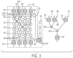
- the dataflow processor 32 may provide for a set of functional units 42 arranged in a mesh 33 formed by interconnecting switches 44.
- the switches 44 are arranged in logical columns extending from input points 46 to corresponding output points 48 to provide parallel data paths therebetween.
- Switches 44 are also arranged in logical rows joined by parallel data paths equal in width to the width of the data paths of the logical columns.
- the functional units 42 are positioned logically between sets of four switches 44 in successive rows and columns to communicate with each of those switches 44 to receive data therefrom or provide data thereto.
- Each switch 44 may therefore generally direct data received at the switch 44 to a switch in an adjacent column or in a lower adjacent row or to up to two lower functional units 42.
- the particular direction of data flow provided by the switch 44 may be determined by a bit value in a mesh 33 configuration switch register 45 associated with the switches 44 determined by a particular configuration image 27 being loaded.
- the data paths provided by the mesh 33 from an input point 46 through successive switches 44 and functional units 42 to an output point 48 will generally be equal to the width of a computer word, for example, thirty-two or sixty-four bits.
- Each of the functional units 42 may implement one of several arithmetic or logical functions but generally fewer functions than provided by the lightweight core 30.
- a given functional unit 42 may implement one or more of integer or floating-point multiplication, subtraction, addition, etc.; and/or logical functions such as shift, compare, bit wise AND, OR, etc.; and/or special-purpose functions such as sigmoid function, transcendental functions, etc.
- the functional units 42 may have a low-power or off state when they are not being used drastically reducing their power consumption.
- the functions that may be implemented by each functional unit 42 may be different for different functional units 42. This particular function provided by a functional unit 42 is determined by a bit value in a mesh 33 configuration function register 47 associated with each of the functional units 42 as set by a loaded configuration image 27.
- While generally the dataflow processor 32 may execute independently from and asynchronously with respect to the lightweight core 30, the data passing through the dataflow processor 32 will be clocked, for example using a self-contained clock element 35, to provide predictable execution.
- data may flow through the mesh 33 of functional units 42 and switches 44 to move generally horizontally and/or downwardly by one step for each clock cycle where a step may be data flow from an input point 46 to a switch 44, or from a switch 44 to a second switch 44, or from a switch 44 to an output point 48, or from a switch 44 to a functional unit 42, or from a functional unit 42 to a switch 44.
- the coordination of operands to arrive at functional units 42 as required by a calculation may be controlled by the interposition of switches (or no-op functional units) in the data path in an amount necessary to obtain the desired delay.
- the necessary routing may be predetermined and incorporated into the configuration image 27 either manually or through use of a special program (such as a complier) for generating configuration images 27.
- the dataflow processor 32 does not provide a program counter or control flow instructions but rather the control flow is determined by the interconnection of the switches 44 and functional units 42. In addition, access to register files or memories by the functional units 42 is not required. Calculations occur as soon as operands are available within the constraint of the clocking which may occur at high speed.
- the functional units 42 may be implemented with dataflow circuitry or with iterating circuitry operating at sufficient speed to complete calculations within one clock cycle. The dataflow processor 32 thus provides extremely fast calculation.
- Each of the input points 46 and output points 48 of the dataflow processor 32 are associated with a first-in, first-out buffer 50 that may be filled asynchronously or emptied asynchronously to the processing performed by the dataflow processor 32 under the control of the stream processor 36.
- the buffers 50 thus provide for parallel data acquisition and data processing.
- each buffer 50 may be provide eight, sixty-four bits words, thus being 8x64 wide and have an arbitrary depth. The invention also contemplates that the different widths may be employed as desired.
- Additional similar buffers 50' independent of input points 46 and output points 48 may be used for storing streaming addresses for indirect loads and stores as will be discussed.
- the input points 46 connect to the respective buffers 50 through an interconnect 41 providing fixed connections allowing given input buffers 50 to communicate with one or more of the first row of switches 44, with each switch 44 receiving data from only one of any of the buffers 50 according to a predefined interconnection pattern. Accordingly, different 64-bit words from a given buffer 50 may be forwarded to different switches 44.
- output points 48 connect to respective buffers 50 through an interconnect 49 providing fixed connections allowing given output points 48 to connect to one or more output buffers 50, each output buffer receiving data from only one of any of the output points 48 according to a predefined interconnection pattern.
- the stream processor 36 provides a simple state machine that can move data autonomously between the memory system 16 and another storage location once it receives program instructions from the lightweight core 30. Generally the stream processor 36 will move input data from the memory system 16 to either the scratchpad memory 34 or the buffers 50, or from the scratchpad memory 34 to the input buffers 50, or may move output data from the scratchpad memory 34 to the memory system 16, or from buffers 50 to the scratchpad memory 34 or the memory system 16 or another butler 50 according to a predefined pattern. In this regard, the stream processor 36 may provide for three separate circuits, one for memory, one for scratchpad, and one for controlling re-cycling of data from output port to input port and also the generation of constant values. These three circuits may operate independently (but for synchronization through the memory access interface 40) for high speed operation.
- the stream processor 36 may also provide for the movement of the data of a configuration image 27 to the mesh 33 configuration registers 45 and 47 of the dataflow processor 32 as is discussed below for configuration.
- the stream processor 36 operates according to configuration instructions, stream instructions, and barrier instructions that may be issued by the lightweight core 30.
- a configuration instruction format is shown in Table I below.
- Table I Configuration Instruction Command Name Parameters Description SD_Config Configuration image address, Size Set dataflow processor configuration from configuration image at address
- This instruction provides the stream processor 36 with the starting address and size of a configuration image 27 in the memory system 16 and operates to load the configuration image 27 into the mesh 33 configuration registers 45 and 47.
- This process will provide the desired configuration of the mesh 33 of the dataflow processor 32 and the functions of the functional units 42 needed for acceleration of the program 22, for example, as triggered by the processor 12 communicating over the control lines 26 to the accelerator 24.
- the stream instructions (shown in Table II) provided by the lightweight core 30 to the stream processor 36 generally identify a source of data, destination data, and the data pattern as follows: Table II Stream Instructions Command Name Parameters Description SD_Mem_Scr Source Memory Address, Access Size, Stride Length, Number of Strides, Destination Scratchpad Address Read from memory system 16 to the scratchpad memory 34 using the indicated access pattern SD_Scr_Port Source Scratchpad Address, Access Size, Stride Length, Number of Strides, Input Port Number Read from scratchpad memory 34 to the designated input point 46 using to the indicated pattern SD_Mem_Port Source Memory Address, Access Size, Stride Length, Number of Strides, Input Port Number Read from memory system 16 to the designated input point 46 using the indicated pattern SD_Const_Port Constant Value, Number of Elements, Destination Port Number Send a series of constant values to the designated input point 46 SD_Chuck Port Number of Elements, Source Port Number Eject a defined series of values from a buffer 50 of
- SD_Port_Scr Source Port Number, Number of elements, Destination Scratchpad address Write a defined series of values from the designated output point 48 to scratchpad memory 34 SD_port_Mem Source Port Number, Access Size, Stride Length, Number of Strides, Destination Memory Address.
- SD_IndPort_Port Indirect Port Number, Offset Address, Destination Port Number Indirect load from memory system 16 based on address data in designated indirect output point 48 for storage in designated destination port SD_Indport_Mem Indirect Port Number, Offset Address, Destination Port Number Indirect store to memory system 16 based on address in indirect port from designated output port
- Indirect addressing is possible using stored data (for example, in a buffer 50') as an address value.
- data for example, from the streaming pattern, is used as the address to obtain further data that is operated on by the functional units 42.
- This indirect addressing effects pointers, useful, for example, when accessing the rows of a sparse matrix.
- the stream processor 36 may provide capability to facilitate indirect access by chaining two streams together, the first stream for accessing a contiguous or strided pattern of pointers, and subsequent streams to load those pointers' values from the memory system 16 and deliver them to the reconfigurable dataflow processor 32. Additional instructions are provided to generate constant values (rather than loading these from memory) and to discard unused output values (as opposed to loading them into nonfunctional memory areas).
- each of these instructions may be issued directly by the processor 12 as part of the instruction set architecture of the accelerator and the data in these instructions used with minimal processing by the lightweight core 30 to control other components of the accelerator.
- the stream processor 36 provides a state machine for autonomous loading or writing data between storage locations using simple patterns of memory access.
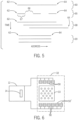
- the simplest pattern is a linear pattern 60 that reads (or writes) sequentially every memory address between a starting address 62 and ending address 64 designated by the instruction. This pattern is indicated by setting the stride length equal to zero.
- the starting address is designated in the above instructions as the source address for reads and the destination address for writes while the ending address is either the number of elements when the source is a port, or a product of the access size times the stride length times the number of strides added to the starting address when the source is the memory or scratchpad.
- the stream processor 36 may be programmed to use a strided pattern 65 by setting the stride length equal to a nonzero value which describes a gap or stride 66 in addresses between access portions 67 defined by the access size.
- an overlapped axis pattern 68 may be invoked by setting the access size to greater than the stride size which signals an overlapping pattern.
- a repeated pattern 69 is easily obtained by setting the stride length to zero with the repetition being provided by the number of strides.
- the lightweight core 30 may also provide for barrier instructions to the stream processor 36 which block the issuance of new memory access instructions until certain previous instructions associated with a data storage resource are complete.
- a barrier instruction shown in Table III below
- Barriers can also be used to signal completion of the calculation to the lightweight core 30.
- Table III-Barrier Instructions Command Name Parameters Description SD_Bar_Scr_Rd - Barrier for Scratchpad Reads SD_Bar_Scr_Wr - Barrier for Scratchpad Writes SD_Bar_All - Barrier to wait for all commands completion
- calculation may provide a data flow graph 70 receiving inputs at input buffers 50 designated A, B and D communicating in this example with single adjacent input points 46. Successive values from buffers 50 associated with ports A and B are provided through appropriate switches 44 to a functional unit 42a to be multiplied together.
- the necessary operands for a given cycle of calculations (being one pass through the mesh 33 from input points 46 to output points 48) are coordinated to be released from the buffers 50 into the mesh 33 at the same time.
- the release of operands may be monitored by a simple ready-monitoring logic, which knows when to trigger a fire signal based on the data 'size' configured for each buffer.
- the invention also contemplates that staggered release from the buffers 50 may be used as part of the synchronization of operands at particular functional units 42 as they pass through the mesh 33.
- the output of functional unit 42a passes through appropriate switches to a functional unit 42b to be added to the value of the buffer 50 associated with input point 46 designated D.
- the data from buffers A and B pass through the same number of switches 44 and functional units 42 before being received at functional unit 42b as the data from port D is being received at the functional unit 42b ensuring that the corresponding data in the buffers 50 are processed in this calculation.
- the configuration image 27 for each particular algorithm executed by the dataflow processor 32 is adjusted to ensure proper coordination of data flow path lengths either manually or through the use of a program such as a compiler.
- a compiler may operate by identifying particular operations of the executed algorithm to sequential time slices according to data dependencies of the data used by the operations, ensuring that operations requiring data dependent on earlier operations are in later time slices.
- the path of data from an input port to each functional units 42 associated with each of the operations may then be adjusted to be equal.
- the path of data from the buffers A, B and D is made equal with the path from buffer A passing through two switches 44 and one functional unit 42a (during four clock cycles) as shown by a dotted line 43a, the path from buffer B passing through two switches 44 and one functional unit 42a (during four clock cycles) as shown by a dotted line 43b, and the path from buffer D passing through three switches 44 (during four clock cycles) as shown by a dotted line 43c.
- a staggered or late release of operands from the buffers 50 may be used to simulate additional clock cycles in some versions of the invention.
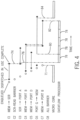
- this calculation may be implemented through eight instructions issued from the lightweight core 30 designated in Fig. 4 as instructions (C1-C8). As depicted, these instructions will be enqueued, dispatched and completed at different times indicated on the horizontal scale. Before the calculation, the dataflow processor 32 is configured by configuration instructions (not shown in this example). Once all of the instructions have been enqueued, the lightweight core 30 may be put into an idle state at time 71.
- the first instruction (C1) provides a transfer from memory system 16 to the scratchpad memory 34 of data that will ultimately used to load the buffer 50 of port A.
- This instruction begins executing immediately after it is enqueued. Is important that the scratchpad memory not be read until it is fully loaded and accordingly the next instruction (C2) provides a scratchpad memory read barrier ensuring that there is no reading of the scratchpad memory 34 until instruction (C1) is complete.
- instruction (C3) which provides a reading of the scratchpad memory 34 into port A, is delayed until completion of instruction (C1) at time 74.
- the barrier instructions may be simply enforced by stalling subsequent commands from the dataflow processor 32 related to the barrier condition allowing all previous commands to proceed in parallel.
- the barrier instruction (C2) does not block instruction (C4) reading memory to the buffer of port B because there is no conflicted resource. Accordingly this transfer process may begin before and continue in parallel with the transfer process of instruction (C3). Similarly transfer from memory system 16 to port D may be performed shortly after this instruction is equeued.
- the writing from port G to memory system 16 concludes releasing the barrier of instruction C8 and signaling to the lightweight core 30 that the calculation is complete so that new instructions may be received from the lightweight core 30.
- the "all" barrier of instruction C8 is released when all of the buffers 50 are empty detected by hardware.
- a second instruction may be enqueued also loading from memory system 16 to Port B.
- a natural barrier is created in the circumstances by the stream processor 36 which serializes loading of buffer 50 intrinsically.
- the second stream for instruction (C7) for loading data into buffer B may not have the same access pattern as the previous one. Also, its type (e.g., source or destination) can be different as well. More generally, the stream commands for a given buffer 50 can change while the dataflow architecture and other stream commands are actively being processed. This leads to more programming flexibility and parallelism.
- the element of the dataflow processor 32 may also be used independently of the stream processor 36, scratchpad memory 34 and lightweight core 30 by having the processor 12 directly handle memory accesses and load and read the buffers 50 as well as provide the memory image files to configure the switches 44 and functional units 42
- This configuration greatly simplifies the architecture; however, it requires the processor 12 to handle memory access patterns. This additional duty performed by the processor 12 may still be efficient when there are long computational runs.
- the buffers 50 may also be increased in size to consolidate memory access operations.
- the lightweight core 30 may also expose hardware parameters of the hardware accelerator 24 including a number and type of functional units 42, a depth of buffers 50 and 50', the size of the scratchpad memory 34, and the longest recurrence (recycling) of data through the dataflow processor 32 for use by a compiler as is generally understood in the art.
- predefined memory access pattern means a limited number of patterns that may be defined prior to the calculation for which the memory accesses require to be performed as opposed to memory access patterns that are a function of calculations made.
- Autonomous as is used herein means without necessary further guidance by the micro core or the data fabric.
- microcontroller should be understood to include any circuit capable of executing the functions described herein including but not necessarily limited to VonNeuman architectures.
Landscapes
- Engineering & Computer Science (AREA)
- Theoretical Computer Science (AREA)
- Software Systems (AREA)
- Physics & Mathematics (AREA)
- General Engineering & Computer Science (AREA)
- General Physics & Mathematics (AREA)
- Computer Hardware Design (AREA)
- Mathematical Physics (AREA)
- Advance Control (AREA)
- Computational Mathematics (AREA)
- Mathematical Analysis (AREA)
- Mathematical Optimization (AREA)
- Pure & Applied Mathematics (AREA)
Description
- The present invention relates to electronic computer architectures and in particular to an application-specific computer accelerator that can be reconfigured for different applications.
- The need for increased computer processing speed and improved energy efficiency has motivated the development of data-parallel architectures like single instruction multiple data (SIMD) machines and general-purpose graphic processing units (GPGPU) machines that can replace general-purpose VonNeuman type processors for many applications. For even more demanding applications such as machine learning and computer vision, these general-purpose data-parallel architectures may be replaced with application-specific accelerators such as the Microsoft Catapult FPGA accelerator, for use in data centers, and Google's Tensor processing unit for distributed machine learning. These application-specific accelerators are normally teamed with a general-purpose, high-performance VonNeuman processor, for example, implementing advanced architectural features including out-of-order execution and speculative execution.
- The special-purpose hardware used in these application-specific accelerators adversely affects the implementation of new processing algorithms. This is because new algorithms, as executed on the special-purpose hardware of an accelerator, normally require a costly redesign and verification of a new architecture. In addition, the narrow functionality of application-specific accelerators limits their value in computer systems where a wide range of applications must be implemented. Finally, to the extent that such application-specific accelerators address niche markets, they may not attract academic interest such as promotes analysis and improvement in these architectures.
- The present inventors have recognized that, despite the wide variety of application-specific accelerators, there are certain common features of the software they execute. Specifically, software executed by application-specific accelerators tends to have simple memory and reuse patterns and high computational intensity in long phases. This in turn suggests that a "general-purpose" application-specific accelerator could be constructed by combining a stream processor that can automatically handle simple memory access patterns with a fast, efficient processor for handling computational intensity. This latter processing requirement can be met by a dataflow processor adapted to be quickly reconfigured. The result is a general-purpose accelerator that is competitive with application-specific accelerators while avoiding the drawbacks associated with special-purpose hardware.
- The invention is defined in claim 1. Further aspects and preferred embodiments are defined in the dependent claims. Any aspects, embodiments and examples of the present disclosure which do not fall under the scope of the appended claims do not form part of the invention and are merely provided for illustrative purposes. Accordingly, in one embodiment, the invention provides a reconfigurable accelerator architecture as defined in claim 1.
- It is thus a feature of at least one embodiment of the invention to implement the common functions of fixed special-purpose accelerators in a reconfigurable accelerator that can implement the function of many special-purpose accelerators. Current simulations suggest the architecture of the present invention can match performance of special-purpose accelerators, providing the advantage of versatility with tolerably small increases in power consumption and circuit area.
- The reconfigurable dataflow processor may provide a set of programmable switches interconnecting functional units in a mesh between input ports receiving input values and output ports providing output values, the functional units providing selectable multiple arithmetic functions, the mesh providing paths from input ports through functional units to output ports determined by the switch programming.
- It is thus a feature of at least one embodiment of the invention to provide a high-speed data flow processor comparable in speed to those found in fixed purpose accelerators and yet rapidly re-reprogrammable, for example, through the use of image files setting the switches and configuring the functional units.
- The mesh may provide direct interconnections between switches and functional units and direct interconnections between switches.
- It is thus a feature of at least one embodiment of the invention to provide a versatile mesh that may both interconnect functional units and bypass functional units.
- The mesh may provide for at least thirty-two parallel data lines, for example, as many as sixty-four parallel data lines, between switches and between switches and functional units.
- It is thus a feature of at least one embodiment of the invention to provide rapid communication of large data words consistent with current processing architectures.
- The functional units may provide different selections of arithmetic and logical operations.
- It is thus a feature of at least one embodiment of the invention to permit the use of heterogeneous functional units allowing a flexible trade-off between versatility and chip area.
- The functional units may operate in parallel.
- It is thus a feature of at least one embodiment of the invention to provide a high degree of parallelism in the computational engine.
- The data flow between functional units may be determined by switch settings and the dataflow processor may further include a clock permitting the moving of data between switches by one switch or between functional units by one functional unit for each clock cycle.
- It is thus a feature of at least one embodiment of the invention to provide a clocking function to allow operands of multistage calculations to be coordinated through switch settings that provide proper selection of their path through the mesh.
- The microcontroller may control the reconfigurable dataflow processor by loading an image file defining programming of the switches and selection of the functions of the functional units.
- It is thus a feature of at least one embodiment of the invention to provide extremely rapid change in configuration of the dataflow processor without the need for compilation.
- The microcontroller may be a VonNeuman, single-issue, in-order core.
- It is thus a feature of at least one embodiment of the invention to provide a flexible circuit for coordinating the elements of the accelerator that requires low-power and small chip areas and that, in some situations, can be used to execute a larger instruction set than possible with the dataflow processor.
- The microcontroller may be further adapted to receive instructions and data from the primary processor to execute logical and arithmetic instructions in response to the instructions and data to return data to the primary processor without involvement of the stream processor or the reconfigurable dataflow processor.
- It is thus a feature of at least one embodiment of the invention to allow the use of the microcontroller without the dataflow processor for certain tasks.
- The stream processor may provide pre-defined memory access patterns including a linear access pattern of contiguous addresses between two memory addresses and a strided access pattern of regularly spaced discontiguous addresses between two memory addresses.
- It is thus a feature of at least one embodiment of the invention to provide memory access patterns commonly used in application-specific acceleration.
- The stream processor may use data obtained with the pre-defined memory access patterns as addresses of data to be used as the multiple input values provided to the reconfigurable dataflow processor.
- It is thus a feature of at least one embodiment of the invention to provide for indirect addressing implementing pointer-type functionality.
- The stream processor may operate autonomously with respect to the microcontroller after programming by the microcontroller.
- It is thus a feature of at least one embodiment of the invention to provide extremely fast memory access operations possible with a dedicated state machine or similar design permitting the dataflow processor to be efficiently focused on calculations only.
- The reconfigurable dataflow processor includes input and output buffers to decoupled access-execute operations permitting operation asynchronously with respect to the stream processor.
- It is thus a feature of at least one embodiment of the invention to permit a decoupling between memory operations and calculations for improved parallelism.
- The microcontroller may issue stream commands to the stream processor defining a data source, a data destination, and an access pattern of data.
- It is thus a feature of at least one embodiment of the invention to provide an extremely simple instruction set for stream processing.
- The microcontroller may further issue barrier commands to the stream processor defining a necessary completion order of memory accesses before and after the barrier command.
- It is thus a feature of at least one embodiment of the invention to provide a simple mechanism for limiting parallelism when necessary to avoid race conditions or problems with data dependencies.
- The computer architecture further includes a scratchpad memory communicating with the stream processor to read data from the memory or write data to the memory as controlled by the stream processor.
- It is thus a feature of at least one embodiment of the invention to eliminate unnecessary memory accesses for improved execution speed.
- The computer architecture may include a single memory interface shared by the scratchpad memory and the reconfigurable dataflow processor.
- It is thus a feature of at least one embodiment of the invention to simplify the elemental component of the accelerator while still allowing high-bandwidth communication with memory among the dataflow processors.
- The microcontroller may respond to predetermined instructions to provide information about the number and type of functional units in the reconfigurable dataflow processor.
- These particular objects and advantages may apply to only some embodiments falling within the claims and thus do not define the scope of the invention.
-
-
Fig. 1 is a block diagram of a processor system employing the reconfigurable application-specific accelerator of the present invention and providing an expanded detail of the accelerator comprised of multiple stream-dataflow processors; -
Fig. 2 is a detailed block diagram of a single stream-dataflow processor showing the combination of a lightweight core with a dataflow mesh, scratchpad memory and stream processor; -
Fig. 3 is a detailed block diagram of the dataflow mesh showing implementation of a simple dataflow graph; -
Fig. 4 is a timing diagram showing processing of a stream of data using the dataflow graph ofFig. 3 such as provides a high degree of parallelism; -
Fig. 5 is a schematic representation of predetermined memory access patterns that can be implemented by the stream processor; and -
Fig. 6 is a block diagram of a processor system using a general-purpose core and the dataflow processor ofFig. 3 directly. - Referring now to
Fig. 1 , acomputer system 10 constructed according to the present invention may provide for a high-performance,VonNeuman processor 12, for example, providing for out-of-order execution and speculative execution of a rich instruction set of arithmetic and logical instructions. Examples ofsuch processors 12 include those manufactured by the Intel Corporation under the trade name of "i7" as well as similar devices manufactured by Advanced Micro Devices, Inc. and ARM Ltd. - The
processor 12 may include anL1 cache 14 for communication with amemory system 16 providing a standard memory hierarchy including but not limited to additional levels ofcache 18 coupled with one or more layers oflarger scale memory 20, for example, composed of random access memory (RAM), disk memory and the like. - The
memory system 16 may store aprogram 22 for execution by thecomputer system 10 such as may benefit from hardware acceleration, for example, including vision processing, machine learning, graph processing or the like. - The
memory system 16 and theprocessor 12 may communicate with areconfigurable hardware accelerator 24, for example, bycontrol lines 26 as well as address anddata lines 23 allowing theprocessor 12 to enlist thehardware accelerator 24 for execution of portions of theprogram 22 amenable to acceleration. Using thecontrol lines 26 and/or data transferred through thememory system 16 by the address anddata lines 23, theprocessor 12 may offload intense calculations having simple memory access patterns to thehardware accelerator 24 for independent execution. In this regard theprocessor 12 coordinates the beginning and conclusion of that execution but may shut down or be used for other tasks during that calculation. During operation, thehardware accelerator 24 may independently access thememory system 16 at the L2 cache in the manner of a multicore processor autonomously without assistance of theprocessor 12. - The
memory system 16 may include a set of configuration files 25 providingconfiguration images 27 that will be used to program a specific application-specific calculation to be performed by thehardware accelerator 24 for the desired portions of theprogram 22. By loadingdifferent configuration images 27, different application-specific calculations may be optimized. Theseconfiguration images 27 may be developed and standardize for particular applications, for example, to provide different functionalities of conventional application-specific accelerators using the current design of thehardware accelerator 24. Generally thehardware accelerator 24 will be invoked using special instructions that will be described below which may be generated by a compiler. - Referring now also to
Fig. 2 , thehardware accelerator 24 may include multiple independently operatingprocessing units 28 that each may receive portions of theprogram 22 to operate in parallel. Eachprocessing unit 28 includes alightweight core 30, adataflow processor 32, ascratchpad memory 34 and astream processor 36. In one embodiment, each of thelightweight core 30,dataflow processor 32,scratchpad memory 34, andstream processor 36 of a givenprocessing unit 28 may share a commonmemory access interface 40 to thememory system 16 to provide independent and parallel memory access among theprocessing units 28. - Generally, the
lightweight core 30 will be a VonNeuman, single-issue, in-order core without speculative execution. Nevertheless, thislightweight core 30 will be able to handle a wider range of different types of arithmetic and logical instructions than thedataflow processor 32 and for this reason may be used by theprocessor 12 for some types of acceleration without involvement of the remainder of theprocessing unit 28 including, for example, thedataflow processor 32. Thelightweight core 30 will require much less integrated circuit area than theprocessor 12 and will use much less power. It will be appreciated that the lightweight core may be any general purpose processor capable of arithmetic and logical functions. - During typical operation, the
lightweight core 30 will issue instructions to thestream processor 36 to load aconfiguration image 27 from thememory system 16 todataflow processor 32 that will configure thedataflow processor 32 for the necessary calculations. Thelightweight core 30 will then issue instructions to thestream processor 36 which in turn will control thememory access interface 40 to obtain information necessary for calculation by thedataflow processor 32 sending this data either directly to thedataflow processor 32 or to ascratchpad memory 34. - The instructions provided by the
lightweight core 30 to thestream processor 36 will include: (1) configuration instructions for configuring thedataflow processor 32 by obtaining and loading andappropriate configuration image 27; (2) stream instructions for providing a stream of data to thedataflow processor 32 without involvement of thelightweight core 30 or theprocessor 12;, and (3) barrier instructions used to enforce some degree of serialization of the instructions executed by theprocessing unit 28 as will be discussed below. - Referring now to
Fig. 3 , thedataflow processor 32 may provide for a set offunctional units 42 arranged in amesh 33 formed by interconnectingswitches 44. Theswitches 44 are arranged in logical columns extending from input points 46 to corresponding output points 48 to provide parallel data paths therebetween.Switches 44 are also arranged in logical rows joined by parallel data paths equal in width to the width of the data paths of the logical columns. Thefunctional units 42 are positioned logically between sets of fourswitches 44 in successive rows and columns to communicate with each of thoseswitches 44 to receive data therefrom or provide data thereto. Eachswitch 44 may therefore generally direct data received at theswitch 44 to a switch in an adjacent column or in a lower adjacent row or to up to two lowerfunctional units 42. - The particular direction of data flow provided by the
switch 44 may be determined by a bit value in amesh 33 configuration switch register 45 associated with theswitches 44 determined by aparticular configuration image 27 being loaded. The data paths provided by themesh 33 from aninput point 46 throughsuccessive switches 44 andfunctional units 42 to anoutput point 48 will generally be equal to the width of a computer word, for example, thirty-two or sixty-four bits. - Each of the
functional units 42 may implement one of several arithmetic or logical functions but generally fewer functions than provided by thelightweight core 30. For example, a givenfunctional unit 42 may implement one or more of integer or floating-point multiplication, subtraction, addition, etc.; and/or logical functions such as shift, compare, bit wise AND, OR, etc.; and/or special-purpose functions such as sigmoid function, transcendental functions, etc. In addition, thefunctional units 42 may have a low-power or off state when they are not being used drastically reducing their power consumption. The functions that may be implemented by eachfunctional unit 42 may be different for differentfunctional units 42. This particular function provided by afunctional unit 42 is determined by a bit value in amesh 33 configuration function register 47 associated with each of thefunctional units 42 as set by a loadedconfiguration image 27. - While generally the
dataflow processor 32 may execute independently from and asynchronously with respect to thelightweight core 30, the data passing through thedataflow processor 32 will be clocked, for example using a self-containedclock element 35, to provide predictable execution. Specifically, data may flow through themesh 33 offunctional units 42 and switches 44 to move generally horizontally and/or downwardly by one step for each clock cycle where a step may be data flow from aninput point 46 to aswitch 44, or from aswitch 44 to asecond switch 44, or from aswitch 44 to anoutput point 48, or from aswitch 44 to afunctional unit 42, or from afunctional unit 42 to aswitch 44. In this way, the coordination of operands to arrive atfunctional units 42 as required by a calculation may be controlled by the interposition of switches (or no-op functional units) in the data path in an amount necessary to obtain the desired delay. The necessary routing may be predetermined and incorporated into theconfiguration image 27 either manually or through use of a special program (such as a complier) for generatingconfiguration images 27. - Generally, the
dataflow processor 32 does not provide a program counter or control flow instructions but rather the control flow is determined by the interconnection of theswitches 44 andfunctional units 42. In addition, access to register files or memories by thefunctional units 42 is not required. Calculations occur as soon as operands are available within the constraint of the clocking which may occur at high speed. Thefunctional units 42 may be implemented with dataflow circuitry or with iterating circuitry operating at sufficient speed to complete calculations within one clock cycle. Thedataflow processor 32 thus provides extremely fast calculation. - Each of the input points 46 and
output points 48 of thedataflow processor 32 are associated with a first-in, first-outbuffer 50 that may be filled asynchronously or emptied asynchronously to the processing performed by thedataflow processor 32 under the control of thestream processor 36. Thebuffers 50 thus provide for parallel data acquisition and data processing. In one embodiment, eachbuffer 50 may be provide eight, sixty-four bits words, thus being 8x64 wide and have an arbitrary depth. The invention also contemplates that the different widths may be employed as desired. Additional similar buffers 50' independent of input points 46 andoutput points 48 may be used for storing streaming addresses for indirect loads and stores as will be discussed. The input points 46 connect to therespective buffers 50 through aninterconnect 41 providing fixed connections allowing given input buffers 50 to communicate with one or more of the first row ofswitches 44, with eachswitch 44 receiving data from only one of any of thebuffers 50 according to a predefined interconnection pattern. Accordingly, different 64-bit words from a givenbuffer 50 may be forwarded todifferent switches 44. - In addition, the output points 48 connect to
respective buffers 50 through aninterconnect 49 providing fixed connections allowing givenoutput points 48 to connect to one ormore output buffers 50, each output buffer receiving data from only one of any of the output points 48 according to a predefined interconnection pattern. - The
stream processor 36 provides a simple state machine that can move data autonomously between thememory system 16 and another storage location once it receives program instructions from thelightweight core 30. Generally thestream processor 36 will move input data from thememory system 16 to either thescratchpad memory 34 or thebuffers 50, or from thescratchpad memory 34 to the input buffers 50, or may move output data from thescratchpad memory 34 to thememory system 16, or frombuffers 50 to thescratchpad memory 34 or thememory system 16 or anotherbutler 50 according to a predefined pattern. In this regard, thestream processor 36 may provide for three separate circuits, one for memory, one for scratchpad, and one for controlling re-cycling of data from output port to input port and also the generation of constant values. These three circuits may operate independently (but for synchronization through the memory access interface 40) for high speed operation. - The
stream processor 36 may also provide for the movement of the data of aconfiguration image 27 to themesh 33 configuration registers 45 and 47 of thedataflow processor 32 as is discussed below for configuration. - More specifically, and as mentioned briefly above, the
stream processor 36 operates according to configuration instructions, stream instructions, and barrier instructions that may be issued by thelightweight core 30. A configuration instruction format is shown in Table I below.Table I - Configuration Instruction Command Name Parameters Description SD_Config Configuration image address, Size Set dataflow processor configuration from configuration image at address - This instruction provides the
stream processor 36 with the starting address and size of aconfiguration image 27 in thememory system 16 and operates to load theconfiguration image 27 into themesh 33 configuration registers 45 and 47. This process will provide the desired configuration of themesh 33 of thedataflow processor 32 and the functions of thefunctional units 42 needed for acceleration of theprogram 22, for example, as triggered by theprocessor 12 communicating over thecontrol lines 26 to theaccelerator 24. - The stream instructions (shown in Table II) provided by the
lightweight core 30 to thestream processor 36 generally identify a source of data, destination data, and the data pattern as follows:Table II Stream Instructions Command Name Parameters Description SD_Mem_Scr Source Memory Address, Access Size, Stride Length, Number of Strides, Destination Scratchpad Address Read from memory system 16 to thescratchpad memory 34 using the indicated access patternSD_Scr_Port Source Scratchpad Address, Access Size, Stride Length, Number of Strides, Input Port Number Read from scratchpad memory 34 to the designatedinput point 46 using to the indicated patternSD_Mem_Port Source Memory Address, Access Size, Stride Length, Number of Strides, Input Port Number Read from memory system 16 to the designatedinput point 46 using the indicated patternSD_Const_Port Constant Value, Number of Elements, Destination Port Number Send a series of constant values to the designated input point 46SD_Chuck Port Number of Elements, Source Port Number Eject a defined series of values from a buffer 50 of the designatedoutput point 48SD_Port_Port Source Port Number, Number of elements, Destination Port Number Recirculate a defined series of values from the designated output point 48 to the designatedinput point 46.SD_Port_Scr Source Port Number, Number of elements, Destination Scratchpad address. Write a defined series of values from the designated output point 48 toscratchpad memory 34SD_port_Mem Source Port Number, Access Size, Stride Length, Number of Strides, Destination Memory Address. Write from the designated output point 48 to memory =system 16 using the indicated patternSD_IndPort_Port Indirect Port Number, Offset Address, Destination Port Number Indirect load from memory system 16 based on address data in designatedindirect output point 48 for storage in designated destination portSD_Indport_Mem Indirect Port Number, Offset Address, Destination Port Number Indirect store to memory system 16 based on address in indirect port from designated output port - These instructions transfer data between storage locations autonomously using a designated pattern as will be discussed below.
- Indirect addressing is possible using stored data (for example, in a buffer 50') as an address value. In indirect addressing, data, for example, from the streaming pattern, is used as the address to obtain further data that is operated on by the
functional units 42. This indirect addressing effects pointers, useful, for example, when accessing the rows of a sparse matrix. Thestream processor 36 may provide capability to facilitate indirect access by chaining two streams together, the first stream for accessing a contiguous or strided pattern of pointers, and subsequent streams to load those pointers' values from thememory system 16 and deliver them to thereconfigurable dataflow processor 32. Additional instructions are provided to generate constant values (rather than loading these from memory) and to discard unused output values (as opposed to loading them into nonfunctional memory areas). - Generally each of these instructions may be issued directly by the
processor 12 as part of the instruction set architecture of the accelerator and the data in these instructions used with minimal processing by thelightweight core 30 to control other components of the accelerator. - Referring now to
Fig. 5 , thestream processor 36 provides a state machine for autonomous loading or writing data between storage locations using simple patterns of memory access. The simplest pattern is alinear pattern 60 that reads (or writes) sequentially every memory address between a startingaddress 62 and endingaddress 64 designated by the instruction. This pattern is indicated by setting the stride length equal to zero. The starting address is designated in the above instructions as the source address for reads and the destination address for writes while the ending address is either the number of elements when the source is a port, or a product of the access size times the stride length times the number of strides added to the starting address when the source is the memory or scratchpad. - Alternatively, the
stream processor 36 may be programmed to use astrided pattern 65 by setting the stride length equal to a nonzero value which describes a gap orstride 66 in addresses betweenaccess portions 67 defined by the access size. - Similarly, an overlapped
axis pattern 68 may be invoked by setting the access size to greater than the stride size which signals an overlapping pattern. A repeatedpattern 69 is easily obtained by setting the stride length to zero with the repetition being provided by the number of strides. - The
lightweight core 30 may also provide for barrier instructions to thestream processor 36 which block the issuance of new memory access instructions until certain previous instructions associated with a data storage resource are complete. For example, a barrier instruction (shown in Table III below) associated with a writing to thescratchpad memory 34 will block subsequent writing to thescratchpad memory 34 until all writings to thescratchpad memory 34 before the barrier instruction are completed. Barriers can also be used to signal completion of the calculation to thelightweight core 30.Table III-Barrier Instructions Command Name Parameters Description SD_Bar_Scr_Rd - Barrier for Scratchpad Reads SD_Bar_Scr_Wr - Barrier for Scratchpad Writes SD_Bar_All - Barrier to wait for all commands completion - Referring now to
Figs. 3 and4 , calculation may provide adata flow graph 70 receiving inputs at input buffers 50 designated A, B and D communicating in this example with single adjacent input points 46. Successive values frombuffers 50 associated with ports A and B are provided throughappropriate switches 44 to afunctional unit 42a to be multiplied together. In the simplest case, the necessary operands for a given cycle of calculations (being one pass through themesh 33 from input points 46 to output points 48) are coordinated to be released from thebuffers 50 into themesh 33 at the same time. The release of operands may be monitored by a simple ready-monitoring logic, which knows when to trigger a fire signal based on the data 'size' configured for each buffer. The invention, however, also contemplates that staggered release from thebuffers 50 may be used as part of the synchronization of operands at particularfunctional units 42 as they pass through themesh 33. The output offunctional unit 42a passes through appropriate switches to afunctional unit 42b to be added to the value of thebuffer 50 associated withinput point 46 designated D. Note that the data from buffers A and B pass through the same number ofswitches 44 andfunctional units 42 before being received atfunctional unit 42b as the data from port D is being received at thefunctional unit 42b ensuring that the corresponding data in thebuffers 50 are processed in this calculation. Theconfiguration image 27 for each particular algorithm executed by thedataflow processor 32 is adjusted to ensure proper coordination of data flow path lengths either manually or through the use of a program such as a compiler. A compiler may operate by identifying particular operations of the executed algorithm to sequential time slices according to data dependencies of the data used by the operations, ensuring that operations requiring data dependent on earlier operations are in later time slices. The path of data from an input port to eachfunctional units 42 associated with each of the operations (clock cycles throughswitches 44 or functional units 42) may then be adjusted to be equal. Thus, for example, for the addition operation atfunctional unit 42a, the path of data from the buffers A, B and D is made equal with the path from buffer A passing through twoswitches 44 and onefunctional unit 42a (during four clock cycles) as shown by a dottedline 43a, the path from buffer B passing through twoswitches 44 and onefunctional unit 42a (during four clock cycles) as shown by a dottedline 43b, and the path from buffer D passing through three switches 44 (during four clock cycles) as shown by a dottedline 43c. A staggered or late release of operands from thebuffers 50 may be used to simulate additional clock cycles in some versions of the invention. - Upon completion of the addition at
functional unit 42b, the output passes tooutput buffer 50 designated G. - Generally this process will be repeated for multiple data value stored in the input ports A and B. Each multiplication at
functional unit 42a being performed concurrently with additions atfunctional unit 42b in the manner of a pipeline and providing for high throughput. - Referring now to
Fig. 4 , this calculation may be implemented through eight instructions issued from thelightweight core 30 designated inFig. 4 as instructions (C1-C8). As depicted, these instructions will be enqueued, dispatched and completed at different times indicated on the horizontal scale. Before the calculation, thedataflow processor 32 is configured by configuration instructions (not shown in this example). Once all of the instructions have been enqueued, thelightweight core 30 may be put into an idle state attime 71. - The first instruction (C1) provides a transfer from
memory system 16 to thescratchpad memory 34 of data that will ultimately used to load thebuffer 50 of port A. This instruction begins executing immediately after it is enqueued. Is important that the scratchpad memory not be read until it is fully loaded and accordingly the next instruction (C2) provides a scratchpad memory read barrier ensuring that there is no reading of thescratchpad memory 34 until instruction (C1) is complete. Accordingly instruction (C3), which provides a reading of thescratchpad memory 34 into port A, is delayed until completion of instruction (C1) attime 74. The barrier instructions may be simply enforced by stalling subsequent commands from thedataflow processor 32 related to the barrier condition allowing all previous commands to proceed in parallel. - The barrier instruction (C2) does not block instruction (C4) reading memory to the buffer of port B because there is no conflicted resource. Accordingly this transfer process may begin before and continue in parallel with the transfer process of instruction (C3). Similarly transfer from
memory system 16 to port D may be performed shortly after this instruction is equeued. - At
time 76 values will be present in each of ports A, B, and D allowing thedataflow processor 32 to begin calculation and these values to be released from theirbuffers 50. These calculations performed by thedataflow processor 32 will be repeated using successive values in each of thebuffers 50 of the input points 46 and provide new calculated values into the output buffers 50 of the output points 48 as indicated by processing cycles 78. - Once the
first processing cycle 78 is completed, attime 80, a writing from the output buffer of port G tomemory system 16 may begin. - After the conclusion of all processing
cycles 78 for the data held in thebuffers 50, attime 82, the writing from port G tomemory system 16 concludes releasing the barrier of instruction C8 and signaling to thelightweight core 30 that the calculation is complete so that new instructions may be received from thelightweight core 30. The "all" barrier of instruction C8 is released when all of thebuffers 50 are empty detected by hardware. - During the processing of instruction (C4), after loading port B from memory, a second instruction (C7) may be enqueued also loading from
memory system 16 to Port B. A natural barrier is created in the circumstances by thestream processor 36 which serializes loading ofbuffer 50 intrinsically. - Also note that the second stream for instruction (C7) for loading data into buffer B may not have the same access pattern as the previous one. Also, its type (e.g., source or destination) can be different as well. More generally, the stream commands for a given
buffer 50 can change while the dataflow architecture and other stream commands are actively being processed. This leads to more programming flexibility and parallelism. - It will be appreciated that substantial parallelism is obtained in this processing provided by the
dataflow processor 32 based on the overlapping line segments indicated inFig. 4 . This, combined with the parallelism obtained by having multiple data flowprocessors 28 that may be enlisted by theprocessor 12, permits extremely fast processing. - Referring now to
Fig. 6 , it will be appreciated that the element of thedataflow processor 32 may also be used independently of thestream processor 36,scratchpad memory 34 andlightweight core 30 by having theprocessor 12 directly handle memory accesses and load and read thebuffers 50 as well as provide the memory image files to configure theswitches 44 andfunctional units 42 This configuration greatly simplifies the architecture; however, it requires theprocessor 12 to handle memory access patterns. This additional duty performed by theprocessor 12 may still be efficient when there are long computational runs. In this case thebuffers 50 may also be increased in size to consolidate memory access operations. - The
lightweight core 30 may also expose hardware parameters of thehardware accelerator 24 including a number and type offunctional units 42, a depth ofbuffers 50 and 50', the size of thescratchpad memory 34, and the longest recurrence (recycling) of data through thedataflow processor 32 for use by a compiler as is generally understood in the art. - As used herein, predefined memory access pattern means a limited number of patterns that may be defined prior to the calculation for which the memory accesses require to be performed as opposed to memory access patterns that are a function of calculations made. Autonomous as is used herein means without necessary further guidance by the micro core or the data fabric.
- Certain terminology is used herein for purposes of reference only, and thus is not intended to be limiting. For example, terms such as "upper", "lower", "above", and "below" refer to directions in the drawings to which reference is made. Terms such as "front", "back", "rear", "bottom" and "side", describe the orientation of portions of the component within a consistent but arbitrary frame of reference which is made clear by reference to the text and the associated drawings describing the component under discussion. Such terminology may include the words specifically mentioned above, derivatives thereof, and words of similar import. Similarly, the terms "first", "second" and other such numerical terms referring to structures do not imply a sequence or order unless clearly indicated by the context.
- When introducing elements or features of the present disclosure and the exemplary embodiments, the articles "a", "an", "the" and "said" are intended to mean that there are one or more of such elements or features. The terms "comprising", "including" and "having" are intended to be inclusive and mean that there may be additional elements or features other than those specifically noted. It is further to be understood that the method steps, processes, and operations described herein are not to be construed as necessarily requiring their performance in the particular order discussed or illustrated, unless specifically identified as an order of performance. It is also to be understood that additional or alternative steps may be employed.
- References to microcontroller should be understood to include any circuit capable of executing the functions described herein including but not necessarily limited to VonNeuman architectures.
- It is specifically intended that the present invention not be limited to the embodiments and illustrations contained herein and the claims should be understood to include modified forms of those embodiments including portions of the embodiments and combinations of elements of different embodiments as come within the invention, which is defined in the following claims.
Claims (15)
- A reconfigurable computer accelerator comprising:a microcontroller (30) adapted to receive instructions and data to control other components of the accelerator;a stream processor (36) receiving instructions from the microcontroller to autonomously read multiple input values stored in a memory (16) according to a selected set of predefined memory access patterns and to autonomously write multiple output values from the accelerator to the memory according to a selected set of predefined memory access patterns;a scratchpad memory (34) communicating with the stream processor to read data from the memory or write data to the memory as controlled by the stream processor;a reconfigurable dataflow processor (32) comprising a plurality of input points (46) and a plurality of output points (48), and configured by the microcontroller to receive the multiple input values to provide output values according to the configuration; anda set of first-in, first-out buffers (50) adapted to communicate data between the memory and the reconfigurable dataflow processor (32), the buffers being emptied or filled under the control of the stream processor (36) asynchronously with respect to the reconfigurable dataflow processor (32) and with respect to the stream processor (36), wherein each of the input points (46) and output points (48) is associated with a respective buffer (50);wherein the stream processor is configured to move data, according to a predefined pattern:between the memory (16) and the scratchpad memory (34)between the memory (16) and the buffers (50);between the scratchpad memory (34) and the buffers (50); andbetween a buffer (50) associated with an output point (48) and a buffer (50) associated with an input point (46).
- The reconfigurable computer accelerator of claim 1, wherein successive instructions from the microcontroller (30) to the stream processor (36) may be received asynchronously with respect to the operation of the dataflow processor (32) and provide for autonomous reading of multiple input values stored in memory or an autonomous writing of multiple output values from the accelerator according to different predefined memory access patterns.
- The reconfigurable computer accelerator of claim 1, wherein the reconfigurable dataflow processor provides a set of programmable switches (44) interconnecting functional units (42) between input ports (46) receiving input values and output ports (48) providing output values, the functional units providing selectable multiple arithmetic functions and the interconnection providing paths from input ports through functional units to output ports determined by the switch programming.
- The reconfigurable computer accelerator of claim 3, wherein the interconnection provides for at least 32 parallel data lines between switches and between switches and functional units.
- The reconfigurable computer accelerator of claim 4, wherein the functional units operate in parallel.
- The reconfigurable computer accelerator of any of claims 3-5, wherein the interconnection provides direct interconnections between switches (44) and functional units (42) and direct interconnections between switches.
- The reconfigurable computer accelerator of any of claims 3-5, wherein the functional units (42) may provide different selections of arithmetic and logical operations.
- The reconfigurable computer accelerator of any of claims 3-5, further including a clock permitting a moving of data between switches by one switch (44) or between functional units by one functional unit (42a) for each clock cycle.
- The reconfigurable computer accelerator of any of claims 3-5, wherein the microcontroller controls the reconfigurable dataflow processor by loading an image file (27) defining programming of the switches and selection of the functions of the functional units.
- The reconfigurable computer accelerator of claim 1, wherein the stream processor (36) operates autonomously with respect to the microcontroller after programming by the microcontroller.
- The reconfigurable computer accelerator of claim 1, wherein the microcontroller (30) issues stream commands to the stream processor defining a data source, a data destination, and an access pattern of data.
- The reconfigurable computer accelerator of claim 11, wherein the microcontroller (30) further issues barrier commands to the stream processor defining a necessary completion order of memory accesses before and after the barrier command.
- The reconfigurable computer accelerator of claim 1, further including a single memory interface (40) shared by the scratchpad memory and the reconfigurable dataflow processor.
- The reconfigurable computer accelerator of claim 1, wherein the microcontroller (30) responds to predetermined instructions to provide information about a number and type of functional units in the reconfigurable dataflow processor
- A computer comprising:an out-of-order, speculative processor core communicating with a memory for receiving instructions and reading and writing data; anda plurality of reconfigurable accelerators controlled by the out-of-order, speculative processor core, wherein each of the plurality of reconfigurable accelerators is the reconfigurable computer accelerator of any one of the preceding claims.
Applications Claiming Priority (2)
| Application Number | Priority Date | Filing Date | Title |
|---|---|---|---|
| US15/416,670 US11853244B2 (en) | 2017-01-26 | 2017-01-26 | Reconfigurable computer accelerator providing stream processor and dataflow processor |
| PCT/US2017/065582 WO2018140140A1 (en) | 2017-01-26 | 2017-12-11 | Reconfigurable, application-specific computer accelerator |
Publications (3)
| Publication Number | Publication Date |
|---|---|
| EP3574401A1 EP3574401A1 (en) | 2019-12-04 |
| EP3574401A4 EP3574401A4 (en) | 2021-01-27 |
| EP3574401B1 true EP3574401B1 (en) | 2023-05-31 |
Family
ID=62907071
Family Applications (1)
| Application Number | Title | Priority Date | Filing Date |
|---|---|---|---|
| EP17894362.7A Active EP3574401B1 (en) | 2017-01-26 | 2017-12-11 | Reconfigurable, application-specific computer accelerator |
Country Status (5)
| Country | Link |
|---|---|
| US (1) | US11853244B2 (en) |
| EP (1) | EP3574401B1 (en) |
| KR (1) | KR102272839B1 (en) |
| CN (1) | CN110214309B (en) |
| WO (1) | WO2018140140A1 (en) |
Families Citing this family (29)
| Publication number | Priority date | Publication date | Assignee | Title |
|---|---|---|---|---|
| WO2013100783A1 (en) | 2011-12-29 | 2013-07-04 | Intel Corporation | Method and system for control signalling in a data path module |
| US10733139B2 (en) | 2017-03-14 | 2020-08-04 | Azurengine Technologies Zhuhai Inc. | Private memory access for a reconfigurable parallel processor using a plurality of chained memory ports |
| US11086816B2 (en) | 2017-09-28 | 2021-08-10 | Intel Corporation | Processors, methods, and systems for debugging a configurable spatial accelerator |
| US10977854B2 (en) | 2018-02-27 | 2021-04-13 | Stmicroelectronics International N.V. | Data volume sculptor for deep learning acceleration |
| US11687762B2 (en) * | 2018-02-27 | 2023-06-27 | Stmicroelectronics S.R.L. | Acceleration unit for a deep learning engine |
| US11586907B2 (en) | 2018-02-27 | 2023-02-21 | Stmicroelectronics S.R.L. | Arithmetic unit for deep learning acceleration |
| US10585725B2 (en) | 2018-03-27 | 2020-03-10 | Arista Networks, Inc. | System and method of hitless reconfiguration of a data processing pipeline |
| US10832370B2 (en) * | 2018-03-27 | 2020-11-10 | Arista Networks, Inc. | System and method of hitless reconfiguration of a data processing pipeline with standby pipeline |
| US11307873B2 (en) | 2018-04-03 | 2022-04-19 | Intel Corporation | Apparatus, methods, and systems for unstructured data flow in a configurable spatial accelerator with predicate propagation and merging |
| US11048661B2 (en) | 2018-04-16 | 2021-06-29 | Simple Machines Inc. | Systems and methods for stream-dataflow acceleration wherein a delay is implemented so as to equalize arrival times of data packets at a destination functional unit |
| US11200186B2 (en) | 2018-06-30 | 2021-12-14 | Intel Corporation | Apparatuses, methods, and systems for operations in a configurable spatial accelerator |
| US10891240B2 (en) | 2018-06-30 | 2021-01-12 | Intel Corporation | Apparatus, methods, and systems for low latency communication in a configurable spatial accelerator |
| CN109189475B (en) * | 2018-08-16 | 2022-06-10 | 北京算能科技有限公司 | Method for constructing instruction set of programmable artificial intelligence accelerator |
| CN109325494B (en) * | 2018-08-27 | 2021-09-17 | 腾讯科技(深圳)有限公司 | Picture processing method, task data processing method and device |
| US10705762B2 (en) * | 2018-08-30 | 2020-07-07 | Micron Technology, Inc. | Forward caching application programming interface systems and methods |
| US11210100B2 (en) | 2019-01-08 | 2021-12-28 | Apple Inc. | Coprocessor operation bundling |
| CN109785224B (en) * | 2019-01-29 | 2021-09-17 | 华中科技大学 | Graph data processing method and system based on FPGA |
| US10817291B2 (en) * | 2019-03-30 | 2020-10-27 | Intel Corporation | Apparatuses, methods, and systems for swizzle operations in a configurable spatial accelerator |
| US10915471B2 (en) | 2019-03-30 | 2021-02-09 | Intel Corporation | Apparatuses, methods, and systems for memory interface circuit allocation in a configurable spatial accelerator |
| US11037050B2 (en) | 2019-06-29 | 2021-06-15 | Intel Corporation | Apparatuses, methods, and systems for memory interface circuit arbitration in a configurable spatial accelerator |
| US11836488B2 (en) | 2020-01-13 | 2023-12-05 | Telefonaktiebolaget Lm Ericsson (Publ) | Accelerator controller for inserting template microcode instructions into a microcode buffer to accelerate matrix operations |
| US11709664B2 (en) | 2020-06-02 | 2023-07-25 | SambaNova Systems, Inc. | Anti-congestion flow control for reconfigurable processors |
| US11237971B1 (en) | 2020-09-16 | 2022-02-01 | SambaNova Systems, Inc. | Compile time logic for detecting streaming compatible and broadcast compatible data access patterns |
| US11645057B2 (en) | 2020-09-24 | 2023-05-09 | SambaNova Systems, Inc. | Systems and methods for memory layout determination and conflict resolution |
| US12086080B2 (en) | 2020-09-26 | 2024-09-10 | Intel Corporation | Apparatuses, methods, and systems for a configurable accelerator having dataflow execution circuits |
| CN113032011B (en) * | 2021-03-12 | 2023-06-27 | 北京睿芯数据流科技有限公司 | Method and system for executing cyclic program in data flow architecture |
| WO2023014033A1 (en) * | 2021-08-02 | 2023-02-09 | Samsung Electronics Co., Ltd. | Method and electronic device for handling resource operating performance configuration in electronic device |
| CN115408104B (en) * | 2022-08-25 | 2023-08-11 | 科东(广州)软件科技有限公司 | Image loading method and device and image generating method and device |
| CN116501504B (en) * | 2023-06-27 | 2023-09-12 | 上海燧原科技有限公司 | Space-time mapping method and device for data stream, electronic equipment and storage medium |
Family Cites Families (21)
| Publication number | Priority date | Publication date | Assignee | Title |
|---|---|---|---|---|
| US7089344B1 (en) * | 2000-06-09 | 2006-08-08 | Motorola, Inc. | Integrated processor platform supporting wireless handheld multi-media devices |
| US7159099B2 (en) * | 2002-06-28 | 2007-01-02 | Motorola, Inc. | Streaming vector processor with reconfigurable interconnection switch |
| US20110238948A1 (en) * | 2002-08-07 | 2011-09-29 | Martin Vorbach | Method and device for coupling a data processing unit and a data processing array |
| US7590823B1 (en) * | 2004-08-06 | 2009-09-15 | Xilinx, Inc. | Method and system for handling an instruction not supported in a coprocessor formed using configurable logic |
| US7941585B2 (en) * | 2004-09-10 | 2011-05-10 | Cavium Networks, Inc. | Local scratchpad and data caching system |
| US7920584B2 (en) | 2005-05-04 | 2011-04-05 | Arm Limited | Data processing system |
| US7856523B2 (en) * | 2005-06-01 | 2010-12-21 | Microsoft Corporation | Random Access Memory (RAM) based Content Addressable Memory (CAM) management |
| US20080244238A1 (en) | 2006-09-01 | 2008-10-02 | Bogdan Mitu | Stream processing accelerator |
| US8122078B2 (en) * | 2006-10-06 | 2012-02-21 | Calos Fund, LLC | Processor with enhanced combined-arithmetic capability |
| US8726289B2 (en) | 2008-02-22 | 2014-05-13 | International Business Machines Corporation | Streaming attachment of hardware accelerators to computer systems |
| US8181003B2 (en) * | 2008-05-29 | 2012-05-15 | Axis Semiconductor, Inc. | Instruction set design, control and communication in programmable microprocessor cores and the like |
| KR101515568B1 (en) * | 2009-02-03 | 2015-04-28 | 삼성전자 주식회사 | Apparatus and method for scheduling instruction processed in reconfigurable array and computing device using these |
| US20120204008A1 (en) * | 2011-02-04 | 2012-08-09 | Qualcomm Incorporated | Processor with a Hybrid Instruction Queue with Instruction Elaboration Between Sections |
| US10078620B2 (en) * | 2011-05-27 | 2018-09-18 | New York University | Runtime reconfigurable dataflow processor with multi-port memory access module |
| US20140201416A1 (en) * | 2013-01-17 | 2014-07-17 | Xockets IP, LLC | Offload processor modules for connection to system memory, and corresponding methods and systems |
| DE112014006183T5 (en) * | 2014-01-16 | 2016-09-22 | Intel Corporation | Apparatus, method and system for a quick configuration mechanism |
| US10591983B2 (en) | 2014-03-14 | 2020-03-17 | Wisconsin Alumni Research Foundation | Computer accelerator system using a trigger architecture memory access processor |
| US20150268963A1 (en) | 2014-03-23 | 2015-09-24 | Technion Research & Development Foundation Ltd. | Execution of data-parallel programs on coarse-grained reconfigurable architecture hardware |
| US11132203B2 (en) * | 2014-08-14 | 2021-09-28 | Texas Instruments Incorporated | System and method for synchronizing instruction execution between a central processor and a coprocessor |
| US9715475B2 (en) | 2015-07-21 | 2017-07-25 | BigStream Solutions, Inc. | Systems and methods for in-line stream processing of distributed dataflow based computations |
| US20170083313A1 (en) * | 2015-09-22 | 2017-03-23 | Qualcomm Incorporated | CONFIGURING COARSE-GRAINED RECONFIGURABLE ARRAYS (CGRAs) FOR DATAFLOW INSTRUCTION BLOCK EXECUTION IN BLOCK-BASED DATAFLOW INSTRUCTION SET ARCHITECTURES (ISAs) |
-
2017
- 2017-01-26 US US15/416,670 patent/US11853244B2/en active Active
- 2017-12-11 EP EP17894362.7A patent/EP3574401B1/en active Active
- 2017-12-11 WO PCT/US2017/065582 patent/WO2018140140A1/en unknown
- 2017-12-11 CN CN201780084864.8A patent/CN110214309B/en active Active
- 2017-12-11 KR KR1020197023744A patent/KR102272839B1/en active IP Right Grant
Also Published As
| Publication number | Publication date |
|---|---|
| WO2018140140A1 (en) | 2018-08-02 |
| KR20190103379A (en) | 2019-09-04 |
| US20180210730A1 (en) | 2018-07-26 |
| EP3574401A1 (en) | 2019-12-04 |
| EP3574401A4 (en) | 2021-01-27 |
| US11853244B2 (en) | 2023-12-26 |
| CN110214309A (en) | 2019-09-06 |
| KR102272839B1 (en) | 2021-07-05 |
| CN110214309B (en) | 2023-10-31 |
Similar Documents
| Publication | Publication Date | Title |
|---|---|---|
| EP3574401B1 (en) | Reconfigurable, application-specific computer accelerator | |
| CN114238204B (en) | Reconfigurable parallel processing | |
| US7873811B1 (en) | Polymorphous computing fabric | |
| JP5364543B2 (en) | A multiprocessor computer architecture incorporating multiple memory algorithm processors in a memory subsystem. | |
| KR101120398B1 (en) | Thread optimized multiprocessor architecture | |
| US10324730B2 (en) | Memory shuffle engine for efficient work execution in a parallel computing system | |
| Falsafi et al. | FPGAs versus GPUs in data centers | |
| US20090119484A1 (en) | Method and Apparatus for Implementing Digital Logic Circuitry | |
| US10761851B2 (en) | Memory apparatus and method for controlling the same | |
| US10659396B2 (en) | Joining data within a reconfigurable fabric | |
| AskariHemmat et al. | RISC-V barrel processor for deep neural network acceleration | |
| US11151077B2 (en) | Computer architecture with fixed program dataflow elements and stream processor | |
| CN101258480A (en) | Processor array with separate serial module | |
| US10990394B2 (en) | Systems and methods for mixed instruction multiple data (xIMD) computing | |
| US11829321B2 (en) | General-purpose systolic array | |
| US20240232127A1 (en) | Dataflow architecture processor statically reconfigurable to perform n-dimensional affine transformation in a tiled manner | |
| US20190004962A1 (en) | Branchless instruction paging in reconfigurable fabric | |
| EP0226103A2 (en) | Address generation for cellular array processors | |
| WO2019006119A1 (en) | Joining data within a reconfigurable fabric | |
| Fei et al. | Using active cache to solve the bottleneck of bus in the parallel Radar signal process system | |
| CN102184089A (en) | Data stream operating method in dynamic reconfigurable processor |
Legal Events
| Date | Code | Title | Description |
|---|---|---|---|
| STAA | Information on the status of an ep patent application or granted ep patent |
Free format text: STATUS: THE INTERNATIONAL PUBLICATION HAS BEEN MADE |
|
| PUAI | Public reference made under article 153(3) epc to a published international application that has entered the european phase |
Free format text: ORIGINAL CODE: 0009012 |
|
| STAA | Information on the status of an ep patent application or granted ep patent |
Free format text: STATUS: REQUEST FOR EXAMINATION WAS MADE |
|
| 17P | Request for examination filed |
Effective date: 20190717 |
|
| AK | Designated contracting states |
Kind code of ref document: A1 Designated state(s): AL AT BE BG CH CY CZ DE DK EE ES FI FR GB GR HR HU IE IS IT LI LT LU LV MC MK MT NL NO PL PT RO RS SE SI SK SM TR |
|
| AX | Request for extension of the european patent |
Extension state: BA ME |
|
| RIN1 | Information on inventor provided before grant (corrected) |
Inventor name: NOWATZKI, ANTHONY Inventor name: SANKARALINGAM, KARTHIKEYAN Inventor name: GANGADHAR, VINAY |
|
| DAV | Request for validation of the european patent (deleted) | ||
| DAX | Request for extension of the european patent (deleted) | ||
| RIC1 | Information provided on ipc code assigned before grant |
Ipc: G06F 13/40 20060101ALI20200917BHEP Ipc: G06F 15/78 20060101ALI20200917BHEP Ipc: G06F 9/448 20180101ALI20200917BHEP Ipc: G06F 13/16 20060101ALI20200917BHEP Ipc: G06F 15/82 20060101ALI20200917BHEP Ipc: G06F 9/30 20180101AFI20200917BHEP Ipc: G06F 9/345 20180101ALI20200917BHEP Ipc: G06F 15/80 20060101ALI20200917BHEP Ipc: G06F 9/38 20180101ALI20200917BHEP |
|
| A4 | Supplementary search report drawn up and despatched |
Effective date: 20210111 |
|
| RIC1 | Information provided on ipc code assigned before grant |
Ipc: G06F 9/30 20180101AFI20201218BHEP Ipc: G06F 15/80 20060101ALI20201218BHEP Ipc: G06F 15/82 20060101ALI20201218BHEP Ipc: G06F 13/16 20060101ALI20201218BHEP Ipc: G06F 13/40 20060101ALI20201218BHEP Ipc: G06F 15/78 20060101ALI20201218BHEP Ipc: G06F 9/38 20180101ALI20201218BHEP Ipc: G06F 9/448 20180101ALI20201218BHEP Ipc: G06F 9/345 20180101ALI20201218BHEP |
|
| STAA | Information on the status of an ep patent application or granted ep patent |
Free format text: STATUS: EXAMINATION IS IN PROGRESS |
|
| 17Q | First examination report despatched |
Effective date: 20210915 |
|
| STAA | Information on the status of an ep patent application or granted ep patent |
Free format text: STATUS: EXAMINATION IS IN PROGRESS |
|
| GRAP | Despatch of communication of intention to grant a patent |
Free format text: ORIGINAL CODE: EPIDOSNIGR1 |
|
| STAA | Information on the status of an ep patent application or granted ep patent |
Free format text: STATUS: GRANT OF PATENT IS INTENDED |
|
| INTG | Intention to grant announced |
Effective date: 20221209 |
|
| GRAS | Grant fee paid |
Free format text: ORIGINAL CODE: EPIDOSNIGR3 |
|
| GRAA | (expected) grant |
Free format text: ORIGINAL CODE: 0009210 |
|
| STAA | Information on the status of an ep patent application or granted ep patent |
Free format text: STATUS: THE PATENT HAS BEEN GRANTED |
|
| AK | Designated contracting states |
Kind code of ref document: B1 Designated state(s): AL AT BE BG CH CY CZ DE DK EE ES FI FR GB GR HR HU IE IS IT LI LT LU LV MC MK MT NL NO PL PT RO RS SE SI SK SM TR |
|
| REG | Reference to a national code |
Ref country code: GB Ref legal event code: FG4D Ref country code: CH Ref legal event code: EP |
|
| REG | Reference to a national code |
Ref country code: DE Ref legal event code: R096 Ref document number: 602017069301 Country of ref document: DE |
|
| REG | Reference to a national code |
Ref country code: AT Ref legal event code: REF Ref document number: 1571329 Country of ref document: AT Kind code of ref document: T Effective date: 20230615 |
|
| P01 | Opt-out of the competence of the unified patent court (upc) registered |
Effective date: 20230512 |
|
| REG | Reference to a national code |
Ref country code: IE Ref legal event code: FG4D |
|
| REG | Reference to a national code |
Ref country code: LT Ref legal event code: MG9D |
|
| REG | Reference to a national code |
Ref country code: NL Ref legal event code: MP Effective date: 20230531 |
|
| REG | Reference to a national code |
Ref country code: AT Ref legal event code: MK05 Ref document number: 1571329 Country of ref document: AT Kind code of ref document: T Effective date: 20230531 |
|
| PG25 | Lapsed in a contracting state [announced via postgrant information from national office to epo] |
Ref country code: SE Free format text: LAPSE BECAUSE OF FAILURE TO SUBMIT A TRANSLATION OF THE DESCRIPTION OR TO PAY THE FEE WITHIN THE PRESCRIBED TIME-LIMIT Effective date: 20230531 Ref country code: NO Free format text: LAPSE BECAUSE OF FAILURE TO SUBMIT A TRANSLATION OF THE DESCRIPTION OR TO PAY THE FEE WITHIN THE PRESCRIBED TIME-LIMIT Effective date: 20230831 Ref country code: ES Free format text: LAPSE BECAUSE OF FAILURE TO SUBMIT A TRANSLATION OF THE DESCRIPTION OR TO PAY THE FEE WITHIN THE PRESCRIBED TIME-LIMIT Effective date: 20230531 Ref country code: AT Free format text: LAPSE BECAUSE OF FAILURE TO SUBMIT A TRANSLATION OF THE DESCRIPTION OR TO PAY THE FEE WITHIN THE PRESCRIBED TIME-LIMIT Effective date: 20230531 |
|
| PG25 | Lapsed in a contracting state [announced via postgrant information from national office to epo] |
Ref country code: RS Free format text: LAPSE BECAUSE OF FAILURE TO SUBMIT A TRANSLATION OF THE DESCRIPTION OR TO PAY THE FEE WITHIN THE PRESCRIBED TIME-LIMIT Effective date: 20230531 Ref country code: PL Free format text: LAPSE BECAUSE OF FAILURE TO SUBMIT A TRANSLATION OF THE DESCRIPTION OR TO PAY THE FEE WITHIN THE PRESCRIBED TIME-LIMIT Effective date: 20230531 Ref country code: NL Free format text: LAPSE BECAUSE OF FAILURE TO SUBMIT A TRANSLATION OF THE DESCRIPTION OR TO PAY THE FEE WITHIN THE PRESCRIBED TIME-LIMIT Effective date: 20230531 Ref country code: LV Free format text: LAPSE BECAUSE OF FAILURE TO SUBMIT A TRANSLATION OF THE DESCRIPTION OR TO PAY THE FEE WITHIN THE PRESCRIBED TIME-LIMIT Effective date: 20230531 Ref country code: LT Free format text: LAPSE BECAUSE OF FAILURE TO SUBMIT A TRANSLATION OF THE DESCRIPTION OR TO PAY THE FEE WITHIN THE PRESCRIBED TIME-LIMIT Effective date: 20230531 Ref country code: IS Free format text: LAPSE BECAUSE OF FAILURE TO SUBMIT A TRANSLATION OF THE DESCRIPTION OR TO PAY THE FEE WITHIN THE PRESCRIBED TIME-LIMIT Effective date: 20230930 Ref country code: HR Free format text: LAPSE BECAUSE OF FAILURE TO SUBMIT A TRANSLATION OF THE DESCRIPTION OR TO PAY THE FEE WITHIN THE PRESCRIBED TIME-LIMIT Effective date: 20230531 Ref country code: GR Free format text: LAPSE BECAUSE OF FAILURE TO SUBMIT A TRANSLATION OF THE DESCRIPTION OR TO PAY THE FEE WITHIN THE PRESCRIBED TIME-LIMIT Effective date: 20230901 |
|
| PG25 | Lapsed in a contracting state [announced via postgrant information from national office to epo] |
Ref country code: FI Free format text: LAPSE BECAUSE OF FAILURE TO SUBMIT A TRANSLATION OF THE DESCRIPTION OR TO PAY THE FEE WITHIN THE PRESCRIBED TIME-LIMIT Effective date: 20230531 |
|
| PG25 | Lapsed in a contracting state [announced via postgrant information from national office to epo] |
Ref country code: SK Free format text: LAPSE BECAUSE OF FAILURE TO SUBMIT A TRANSLATION OF THE DESCRIPTION OR TO PAY THE FEE WITHIN THE PRESCRIBED TIME-LIMIT Effective date: 20230531 |
|
| PG25 | Lapsed in a contracting state [announced via postgrant information from national office to epo] |
Ref country code: SM Free format text: LAPSE BECAUSE OF FAILURE TO SUBMIT A TRANSLATION OF THE DESCRIPTION OR TO PAY THE FEE WITHIN THE PRESCRIBED TIME-LIMIT Effective date: 20230531 Ref country code: SK Free format text: LAPSE BECAUSE OF FAILURE TO SUBMIT A TRANSLATION OF THE DESCRIPTION OR TO PAY THE FEE WITHIN THE PRESCRIBED TIME-LIMIT Effective date: 20230531 Ref country code: RO Free format text: LAPSE BECAUSE OF FAILURE TO SUBMIT A TRANSLATION OF THE DESCRIPTION OR TO PAY THE FEE WITHIN THE PRESCRIBED TIME-LIMIT Effective date: 20230531 Ref country code: PT Free format text: LAPSE BECAUSE OF FAILURE TO SUBMIT A TRANSLATION OF THE DESCRIPTION OR TO PAY THE FEE WITHIN THE PRESCRIBED TIME-LIMIT Effective date: 20231002 Ref country code: EE Free format text: LAPSE BECAUSE OF FAILURE TO SUBMIT A TRANSLATION OF THE DESCRIPTION OR TO PAY THE FEE WITHIN THE PRESCRIBED TIME-LIMIT Effective date: 20230531 Ref country code: DK Free format text: LAPSE BECAUSE OF FAILURE TO SUBMIT A TRANSLATION OF THE DESCRIPTION OR TO PAY THE FEE WITHIN THE PRESCRIBED TIME-LIMIT Effective date: 20230531 Ref country code: CZ Free format text: LAPSE BECAUSE OF FAILURE TO SUBMIT A TRANSLATION OF THE DESCRIPTION OR TO PAY THE FEE WITHIN THE PRESCRIBED TIME-LIMIT Effective date: 20230531 |
|
| REG | Reference to a national code |
Ref country code: DE Ref legal event code: R097 Ref document number: 602017069301 Country of ref document: DE |
|
| PLBE | No opposition filed within time limit |
Free format text: ORIGINAL CODE: 0009261 |
|
| STAA | Information on the status of an ep patent application or granted ep patent |
Free format text: STATUS: NO OPPOSITION FILED WITHIN TIME LIMIT |
|
| PGFP | Annual fee paid to national office [announced via postgrant information from national office to epo] |
Ref country code: DE Payment date: 20240124 Year of fee payment: 7 Ref country code: GB Payment date: 20240125 Year of fee payment: 7 |
|
| PG25 | Lapsed in a contracting state [announced via postgrant information from national office to epo] |
Ref country code: SI Free format text: LAPSE BECAUSE OF FAILURE TO SUBMIT A TRANSLATION OF THE DESCRIPTION OR TO PAY THE FEE WITHIN THE PRESCRIBED TIME-LIMIT Effective date: 20230531 |
|
| 26N | No opposition filed |
Effective date: 20240301 |
|
| PG25 | Lapsed in a contracting state [announced via postgrant information from national office to epo] |
Ref country code: SI Free format text: LAPSE BECAUSE OF FAILURE TO SUBMIT A TRANSLATION OF THE DESCRIPTION OR TO PAY THE FEE WITHIN THE PRESCRIBED TIME-LIMIT Effective date: 20230531 Ref country code: IT Free format text: LAPSE BECAUSE OF FAILURE TO SUBMIT A TRANSLATION OF THE DESCRIPTION OR TO PAY THE FEE WITHIN THE PRESCRIBED TIME-LIMIT Effective date: 20230531 |
|
| PGFP | Annual fee paid to national office [announced via postgrant information from national office to epo] |
Ref country code: FR Payment date: 20240214 Year of fee payment: 7 |
|
| REG | Reference to a national code |
Ref country code: CH Ref legal event code: PL |
|
| PG25 | Lapsed in a contracting state [announced via postgrant information from national office to epo] |
Ref country code: LU Free format text: LAPSE BECAUSE OF NON-PAYMENT OF DUE FEES Effective date: 20231211 |
|
| PG25 | Lapsed in a contracting state [announced via postgrant information from national office to epo] |
Ref country code: MC Free format text: LAPSE BECAUSE OF FAILURE TO SUBMIT A TRANSLATION OF THE DESCRIPTION OR TO PAY THE FEE WITHIN THE PRESCRIBED TIME-LIMIT Effective date: 20230531 |
|
| REG | Reference to a national code |
Ref country code: BE Ref legal event code: MM Effective date: 20231231 |
|
| PG25 | Lapsed in a contracting state [announced via postgrant information from national office to epo] |
Ref country code: MC Free format text: LAPSE BECAUSE OF FAILURE TO SUBMIT A TRANSLATION OF THE DESCRIPTION OR TO PAY THE FEE WITHIN THE PRESCRIBED TIME-LIMIT Effective date: 20230531 Ref country code: LU Free format text: LAPSE BECAUSE OF NON-PAYMENT OF DUE FEES Effective date: 20231211 |
|
| REG | Reference to a national code |
Ref country code: IE Ref legal event code: MM4A |
|
| PG25 | Lapsed in a contracting state [announced via postgrant information from national office to epo] |
Ref country code: IE Free format text: LAPSE BECAUSE OF NON-PAYMENT OF DUE FEES Effective date: 20231211 |
|
| PG25 | Lapsed in a contracting state [announced via postgrant information from national office to epo] |
Ref country code: BE Free format text: LAPSE BECAUSE OF NON-PAYMENT OF DUE FEES Effective date: 20231231 |
|
| PG25 | Lapsed in a contracting state [announced via postgrant information from national office to epo] |
Ref country code: CH Free format text: LAPSE BECAUSE OF NON-PAYMENT OF DUE FEES Effective date: 20231231 |
|
| PG25 | Lapsed in a contracting state [announced via postgrant information from national office to epo] |
Ref country code: IE Free format text: LAPSE BECAUSE OF NON-PAYMENT OF DUE FEES Effective date: 20231211 Ref country code: CH Free format text: LAPSE BECAUSE OF NON-PAYMENT OF DUE FEES Effective date: 20231231 Ref country code: BE Free format text: LAPSE BECAUSE OF NON-PAYMENT OF DUE FEES Effective date: 20231231 |