EP3573230B1 - Solar cell module error determination system and method - Google Patents
Solar cell module error determination system and method Download PDFInfo
- Publication number
- EP3573230B1 EP3573230B1 EP17893323.0A EP17893323A EP3573230B1 EP 3573230 B1 EP3573230 B1 EP 3573230B1 EP 17893323 A EP17893323 A EP 17893323A EP 3573230 B1 EP3573230 B1 EP 3573230B1
- Authority
- EP
- European Patent Office
- Prior art keywords
- photovoltaic
- photovoltaic module
- amplifier
- lock
- photovoltaic cell
- Prior art date
- Legal status (The legal status is an assumption and is not a legal conclusion. Google has not performed a legal analysis and makes no representation as to the accuracy of the status listed.)
- Active
Links
Images




Classifications
-
- H—ELECTRICITY
- H02—GENERATION; CONVERSION OR DISTRIBUTION OF ELECTRIC POWER
- H02S—GENERATION OF ELECTRIC POWER BY CONVERSION OF INFRARED RADIATION, VISIBLE LIGHT OR ULTRAVIOLET LIGHT, e.g. USING PHOTOVOLTAIC [PV] MODULES
- H02S50/00—Monitoring or testing of PV systems, e.g. load balancing or fault identification
- H02S50/10—Testing of PV devices, e.g. of PV modules or single PV cells
- H02S50/15—Testing of PV devices, e.g. of PV modules or single PV cells using optical means, e.g. using electroluminescence
-
- H—ELECTRICITY
- H02—GENERATION; CONVERSION OR DISTRIBUTION OF ELECTRIC POWER
- H02S—GENERATION OF ELECTRIC POWER BY CONVERSION OF INFRARED RADIATION, VISIBLE LIGHT OR ULTRAVIOLET LIGHT, e.g. USING PHOTOVOLTAIC [PV] MODULES
- H02S10/00—PV power plants; Combinations of PV energy systems with other systems for the generation of electric power
- H02S10/40—Mobile PV generator systems
-
- Y—GENERAL TAGGING OF NEW TECHNOLOGICAL DEVELOPMENTS; GENERAL TAGGING OF CROSS-SECTIONAL TECHNOLOGIES SPANNING OVER SEVERAL SECTIONS OF THE IPC; TECHNICAL SUBJECTS COVERED BY FORMER USPC CROSS-REFERENCE ART COLLECTIONS [XRACs] AND DIGESTS
- Y02—TECHNOLOGIES OR APPLICATIONS FOR MITIGATION OR ADAPTATION AGAINST CLIMATE CHANGE
- Y02E—REDUCTION OF GREENHOUSE GAS [GHG] EMISSIONS, RELATED TO ENERGY GENERATION, TRANSMISSION OR DISTRIBUTION
- Y02E10/00—Energy generation through renewable energy sources
- Y02E10/50—Photovoltaic [PV] energy
Definitions
- the present invention relates to an abnormality determination system and method for a photovoltaic module.
- Patent Document 1 Japanese Unexamined Patent Application, First Publication No. 2013-131679
- a failed cell shows a decrease in a power current and also shows a reverse voltage and a hot spot state. Therefore, when a cell voltage or cell temperature of an individual photovoltaic cell included in a photovoltaic module is monitored, a failed cell can be discovered.
- a photovoltaic module is normally sealed with a resin. Therefore, a cell voltage of an individual photovoltaic cell may not be measured.
- a cell temperature can be easily observed by an infrared camera, but the cell temperature is strongly influenced by an ambient environment. Therefore, when failure of a cell is determined according to only a cell temperature, precision of determination of whether the cell has failed may be lowered.
- the present invention is devised to solve the foregoing problems and an object of the present invention is to provide an abnormality determination system and method for a photovoltaic module capable of accurately determining which photovoltaic cell is in an abnormal state among a plurality of photovoltaic cells connected in series.
- an abnormality determination system for a photovoltaic module as recited in claim 1 and a corresponding method as recited in claim 6. Further advantageous embodiments are recited in the dependent claims.
- an abnormality determination system and method for a photovoltaic module capable of accurately determining which photovoltaic cell is in an abnormal state among a plurality of photovoltaic cells connected in series.
- Fig. 1 is a diagram showing an example of the configuration of the abnormality determination system 1 for the photovoltaic module M according to the first embodiment.
- the abnormality determination system 1 is applied to a photovoltaic module M.
- the photovoltaic module M includes a plurality of photovoltaic cells C1, C2, C3, C4, and C5 connected in series.
- the photovoltaic module M is connected to a load resistor R.
- the photovoltaic module M includes five photovoltaic cells C1, C2, C3, C4, and C5.
- the photovoltaic module M may include any number of plural photovoltaic cells connected in series other than five.
- the abnormality determination system 1 includes a modulated light radiation unit 11, a phase detection unit 12, a determination unit 13, and an output unit 14.
- the modulated light radiation unit 11 includes a laser radiation unit 111, a light chopper unit 112, a chopper control unit 113, a reflector 114, and a filter 115.
- the laser radiation unit 111 radiates, for example, a laser such as a He-Ne laser.
- the modulated light radiation unit 11 includes the laser radiation unit 111.
- the modulated light radiation unit 11 may include a radiation unit that radiates light other than a laser.
- the light chopper unit 112 modulates the laser radiated from the laser radiation unit 111 into modulated light ML with a predetermined phase (frequency).
- the chopper control unit 113 controls the light chopper unit 112.
- the chopper control unit 113 outputs a reference signal RS indicating the phase (frequency) of the modulated light ML modulated by the light chopper unit 112.
- the filter 115 reduces the modulated light ML modulated by the light chopper unit 112.
- the filter 115 is, for example, a neutral density (ND) filter.
- the reflector 114 reflects the modulated light ML reduced by the filter 115.
- the modulated light ML reflected by the reflector 114 is radiated to the photovoltaic cell C3.
- the modulated light ML reflected by the reflector 114 is radiated to the photovoltaic cell C3.
- the modulated light ML reflected by the reflector 114 may be radiated to any of the photovoltaic cells C1, C2, C4, and C5 other than the photovoltaic cell C3.
- the reflector 114 may be omitted.
- the light chopper unit 112, the filter 115, and the reflector 114 are arranged in the order of the light chopper unit 112, the filter 115, and the reflector 114 between the laser radiation unit 111 and the photovoltaic module M.
- the order of the light chopper unit 112, the filter 115, and the reflector 114 may be set to be different.
- the modulated light radiation unit 11 radiates the modulated light ML to one photovoltaic cell C3 among the plurality of photovoltaic cells C1, C2, C3, C4, and C5 included in the photovoltaic module M.
- the phase detection unit 12 includes a lock-in amplifier 12a. Specifically, the phase detection unit 12 is the lock-in amplifier 12a.
- the lock-in amplifier 12a is connected to the photovoltaic module M. Specifically, a power output voltage Vo of the photovoltaic module M is input as an input signal to the lock-in amplifier 12a.
- the reference signal RS output from the chopper control unit 113 is input to the lock-in amplifier 12a.
- the lock-in amplifier 12a outputs a signal LAo in accordance with a state of the photovoltaic cell C3.
- Fig. 2 is a diagram showing an example of a configuration of an abnormality determination system for a photovoltaic module according to a first modification example of the first embodiment.
- a minute resistor r for current detection is connected in series to a circuit connecting the photovoltaic module M and the load resistor R.
- the power output voltage Vo of the photovoltaic module M exceeds a voltage upper limit of the input signal of the lock-in amplifier 12a
- a voltage applied to the minute resistor r for current detection and set in a range below the voltage upper limit of the input signal of the lock-in amplifier 12a is given as an input signal of the lock-in amplifier 12a.
- Fig. 3 is a diagram showing an example of a configuration of an abnormality determination system for a photovoltaic module according to a second modification example of the first embodiment.
- a capacitor C or a highpass filter suppressing the power output voltage Vo which is a direct-current voltage or a bandpass filter (not shown) passing an alternating-current component close to a frequency of the modulated light ML is inserted into a conducting wire of an input signal to the lock-in amplifier 12a.
- the reference signal RS input to the lock-in amplifier 12a indicates a phase (frequency) of the modulated light ML radiated from the modulated light radiation unit 11 to the photovoltaic cell C3.
- the signal LAo output from the lock-in amplifier 12a indicates a state of the photovoltaic cell C3 to which the modulated light ML is radiated.
- the phase detection unit 12 outputs the signal LAo in accordance with the state of the photovoltaic cell C3 according to a signal indicating a power output of the photovoltaic module M and the reference signal RS indicating the phase (frequency) of the modulated light ML.
- the phase detection unit 12 outputs the signal LAo in accordance with the state of the photovoltaic cell C3.
- the signal LAo output from the lock-in amplifier 12a is input to the determination unit 13.
- the determination unit 13 determines whether the photovoltaic cell C3 is in an abnormal state according to the signal LAo output from the phase detection unit 12.
- a determination result in the determination unit 13, that is, whether the photovoltaic cell C3 is in the abnormal state is output by the output unit 14.
- the output unit 14 includes at least one of a display unit that displays the determination result in the determination unit 13, a sound output unit that outputs a sound of the determination result in the determination unit 13, and a printing unit that prints the determination result in the determination unit 13.
- a user of the abnormality determination system 1 can ascertain whether the photovoltaic cell C3 is in the abnormal state in accordance with the determination result in the determination unit 13 output from the output unit 14.
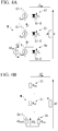
- Fig. 4A is an equivalent circuit diagram showing the photovoltaic module M and the load resistor R shown in Fig. 1 .
- the five photovoltaic cells C1, C2, C3, C4, and C5 are connected in series, but in an example shown in Fig. 4A , n photovoltaic cells C1, ..., Ci, ..., and Cn are connected in series.
- the photovoltaic cell C1 is expressed by a current source C1-1 outputting a current I ph1 and a diode C1-2.
- the photovoltaic cell Ci is expressed by a current source Ci-1 outputting a current I phi and a diode Ci-2.
- the photovoltaic cell Cn is expressed by a current source Cn-1 outputting a current I phn and a diode Cn-2.
- I denotes a current flowing in the entire photovoltaic module M and the load resistor R.
- I 0i denotes a reverse saturation current of the diode Ci-2 and q denotes an elementary charge.
- Vi denotes a forward voltage of the diode Ci-2
- n denotes a diode factor
- k denotes a Boltzmann constant
- T denotes an absolute temperature
- the modulated light ML is radiated from the modulated light radiation unit 11 to the photovoltaic cell C3.
- the modulated light ML is radiated from the modulated light radiation unit 11 to the photovoltaic cell Cn.
- a photocurrent of the photovoltaic cell Cn increases by a minute amount ⁇ I ph .
- the variation amount is as indicated in Fig. 4B .
- Fig. 4B is an equivalent circuit diagram showing a minute change ⁇ I in the current I flowing in the photovoltaic module M and the load resistor R shown in Fig. 4A .
- the photovoltaic cell C1 is expressed by a differential resistor R d1 .
- the current source C1-1 (see Fig. 4A ) from the photocurrent of the photovoltaic cell C1 is opened and lost.
- the diode C1-2 (see Fig. 4A ) of the photovoltaic cell C1 is expressed by the differential resistor R d1 .
- the photovoltaic cell Ci is expressed by the differential resistor R d1 .
- the photovoltaic cell Cn to which the modulated light ML from the modulated light radiation unit 11 is radiated is expressed by the current source Cn-1 outputting a minute change ⁇ I phn of the current and a differential resistor R dn .
- Fig. 5 is a modified diagram of the equivalent circuit diagram shown in Fig. 4B .
- a change ⁇ V n of the voltage of the photovoltaic cell Cn is expressed by Expression (3-1) below.
- a change ⁇ V of a voltage applied to the load resistor R is expressed by Expression (3-3) below.
- the denominator of the right side of Expression (3-3) is a sum of differential resistors of all the photovoltaic cells C1, ..., Ci, ..., Cn. Therefore, when the value of the differential resistor is not changed, the denominator of the right side Expression (3-3) is the same despite occurrence of the change ⁇ I phn in the current in a certain photovoltaic cell.
- the power output voltage Vo of the photovoltaic module M that is, the voltage applied to the load resistor R
- the lock-in amplifier 12a the change ⁇ V in the voltage applied to the load resistor R is obtained by the lock-in amplifier 12a.
- the differential resistor R dn of the photovoltaic cell Cn is larger.
- the photocurrent I phn of the photovoltaic cell Cn is the minimum, the current I flowing in the entire photovoltaic module M and the load resistor R is equal to the photocurrent I phn and the differential resistor R dn of the photovoltaic cell Cn becomes the maximum.
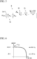
- Fig. 6 is a diagram showing a correlation between a current I output by the photovoltaic cell Ci in which incident sunlight is constant, that is, the photovoltaic cell Ci in which a current output by the current source I phi is constant, and a voltage applied to the photovoltaic cell Ci, that is, a voltage applied to the differential resistor R di .
- the horizontal axis represents a voltage applied to the differential resistor R di .
- the vertical axis represents the current I output by the photovoltaic cell Ci.
- the voltage applied to the differential resistor R di increases as the current I output by the photovoltaic cell Ci decreases.
- the differential resistor R di increases. Conversely, when the current I output by the photovoltaic cell Ci is small and the voltage applied to the differential resistor R di is large, the differential resistor R di decreases.
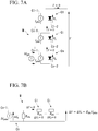
- Fig. 7A is an equivalent circuit diagram showing the opened photovoltaic module M.
- Fig. 7B is an equivalent circuit diagram showing the opened photovoltaic module M shown in Fig. 7A and a minute change ⁇ V in the power output voltage Vo.
- the photovoltaic module M is not opened. In the examples shown in Figs. 7A and 7B , however, the photovoltaic module M is opened.
- a weak component synchronized with the modulated light ML is included in the power output voltage Vo of the photovoltaic module M output to the lock-in amplifier 12a when the weak modulated light ML is radiated to only the photovoltaic cell Cn in the photovoltaic module M during generation.
- the weak component is considered to have information in which a state (for example, an operation point of the photovoltaic cell Cn, whether the photovoltaic cell Cn fails) of the photovoltaic cell Cn to which the weak modulated light ML is radiated is reflected.
- the power output voltage Vo of the photovoltaic module M and the reference signal RS indicating the phase (frequency) of the modulated light ML radiated to the photovoltaic cell C3 are input to the lock-in amplifier 12a.
- the lock-in amplifier 12a extracts a weak component synchronized with the modulated light ML.
- the lock-in amplifier 12a outputs the signal LAo in accordance with the state of the photovoltaic cell C3 to the determination unit 13. Therefore, in the example shown in Fig. 1 , information regarding the state of the photovoltaic cell C3 can be obtained quantitatively and the determination unit 13 can determine whether the photovoltaic cell C3 is in an abnormal state.
- the present inventors carried out an experiment in which an output voltage of the lock-in amplifier 12a in the case of radiation of the modulated light ML to the photovoltaic cell which is in an abnormal state (that is, failure) was compared to an output voltage of the lock-in amplifier 12a in the case of radiation of the modulated light ML to the photovoltaic cell which is not in an abnormal state (that is, non-failure).
- the photovoltaic module M including five photovoltaic cells C1, C2, C3, C4, and C5 connected in series was used.
- the photovoltaic cell C5 or the photovoltaic cell C1 was set to an abnormal state (that is, a state in which normal generation was not possible) by masking the photovoltaic cell C5 or the photovoltaic cell C1.
- the photovoltaic cells C2, C3, and C4 were set to a normal state (that is, a state in which normal generation was possible) by not masking the photovoltaic cells C2, C3, and C4.
- the power output voltage Vo of the photovoltaic module M was measured.
- the power output voltage Vo was input as an input signal to the lock-in amplifier 12a.
- a voltage of each of the photovoltaic cells C1, C2, C3, C4, and C5 was measured.
- the modulated light radiation unit 11 was configured as in the example shown in Fig. 1 .
- an LED was used to radiate light simulated sunlight to the photovoltaic cells C1, C2, C3, C4, and C5 rather than sunlight.
- Fig. 8 is a diagram showing a result of a demonstration experiment.
- Fig. 8 “cell 1" refers to the photovoltaic cell C1
- cell 2 refers to the photovoltaic cell C2
- cell 3 refers to the photovoltaic cell C3
- cell 4" refers to the photovoltaic cell C4
- cell 5" refers to the photovoltaic cell C5.
- the “average of voltages (V)" of “cell 1” refers to a voltage (V) of the photovoltaic cell C1
- the “average of voltages (V)” of “cell 2” refers to a voltage (V) of the photovoltaic cell C2
- the “average of voltages (V)” of “cell 3” refers to a voltage (V) of the photovoltaic cell C3
- the “average of voltages (V)” of “cell 4" refers to a voltage (V) of the photovoltaic cell C4
- the “average of voltages (V)" of "cell 5" refers to a voltage (V) of the photovoltaic cell C5.
- the "average of voltages (V)" of a “module” refers to a power output voltage Vo (V) of the photovoltaic module M configured by connecting the photovoltaic cells C1, C2, C3, C4, and C5 in series.
- the "average of voltages (V)" of a “lock-in amplifier” refers to a voltage (V) of the signal LAo output from the lock-in amplifier 12a when the power output voltage Vo of the photovoltaic module M and the reference signal RS indicating the phase (frequency) of the modulated light ML are input to the lock-in amplifier 12a.
- condition 1, condition 2, and condition 3 were set.
- condition 1 none of the photovoltaic cells C1, C2, C3, C4, and C5 were masked. That is, a normal state was set in all of the photovoltaic cells C1, C2, C3, C4, and C5. Simulated sunlight was radiated to all of the photovoltaic cells C1, C2, C3, C4, and C5. The modulated light ML was radiated from the modulated light radiation unit 11 to only the photovoltaic cell C5.
- the power output voltage Vo of the photovoltaic module M became 1.368 (V).
- the output voltage of the lock-in amplifier 12a became 0.085 (V).
- the voltage of the photovoltaic cell C5 in the normal state belongs to a group in which the voltage is higher among the voltages of the other photovoltaic cells C1 to C4 according to condition 1 of Fig. 8 , and thus a differential resistor R d5 of the photovoltaic cell C5 belongs to a group in which the differential resistance is smaller.
- the differential resistance is small, the change ⁇ V in the voltage applied to the load resistor R decreases from Expression (3-3). Therefore, the output voltage of the lock-in amplifier 12a decreases.
- condition 2 the photovoltaic cell C5 was masked without masking the photovoltaic cells C1, C2, C3, and C4. That is, a normal state was set in the photovoltaic cells C1, C2, C3, and C4 and an abnormal state was set in the photovoltaic cell C5. Simulated sunlight was radiated to all of the photovoltaic cells C1, C2, C3, C4, and C5. The modulated light ML was radiated to only the photovoltaic cell C5 set to the abnormal state.
- the power output voltage Vo of the photovoltaic module M became 1.276 (V).
- the output voltage of the lock-in amplifier 12a became 3.590 (V).
- the voltage of the photovoltaic cell C5 in the abnormal state is the smallest in comparison with the voltages of the other photovoltaic cells C1 to C4 according to condition 2 of Fig. 8 , and thus the differential resistor R d5 of the photovoltaic cell C5 becomes the largest.
- the differential resistance is large, the change ⁇ V in the voltage applied to the load resistor R increases from Expression (3-3). Therefore, the output voltage of the lock-in amplifier 12a increases.
- condition 2 in which the photovoltaic cell C5 was set to the abnormal state, the power amount of the entire photovoltaic module M was lowered and the power output voltage Vo of the photovoltaic module M was lowered than in condition 1 in which all of the photovoltaic cells C1, C2, C3, C4, and C5 were set to the normal state.
- condition 2 in which the modulated light ML was radiated to the photovoltaic cell C5 set to the abnormal state, the output voltage of the lock-in amplifier 12a was raised further than in condition 1 in which the modulated light ML was radiated to the photovoltaic cell C5 set to the normal state.
- condition 3 the photovoltaic cell C1 was masked without masking the photovoltaic cells C2, C3, C4, and C5. That is, a normal state was set in the photovoltaic cells C2, C3, C4, and C5 and an abnormal state was set in the photovoltaic cell C1. Simulated sunlight was radiated to all of the photovoltaic cells C1, C2, C3, C4, and C5. The modulated light ML was radiated to only the photovoltaic cell C5 set to the normal state.
- the power output voltage Vo of the photovoltaic module M became 1.075 (V).
- the output voltage of the lock-in amplifier 12a became 0.037 (V).
- the voltage of the photovoltaic cell C5 in the normal state belongs to a group in which the voltage is higher among the voltages of the other photovoltaic cells C1 to C4 according to condition 3 of Fig. 8 , and thus the differential resistor R d5 of the photovoltaic cell C5 belongs to a group in which the differential resistance is smaller.
- the differential resistance is small, the change ⁇ V in the voltage applied to the load resistor R decreases from Expression (3-3). Therefore, the output voltage of the lock-in amplifier 12a decreases.
- condition 3 in which the photovoltaic cell C1 was set to the abnormal state, the power amount of the entire photovoltaic module M was lowered and the power output voltage Vo of the photovoltaic module M was lowered than in condition 1 in which all of the photovoltaic cells C1, C2, C3, C4, and C5 were set to the normal state.
- the present inventors found that when the modulated light ML was radiated to the photovoltaic cell in the abnormal state, the output voltage of the lock-in amplifier 12a was higher than the output voltage of the lock-in amplifier 12a when the modulated light ML was radiated to the photovoltaic cell in the normal state.
- the present inventors found that when the photovoltaic cell to which the modulated light ML was radiated was in the abnormal state, the lock-in amplifier 12a output a higher voltage than when the photovoltaic cell to which the modulated light ML was radiated was in the normal state.
- the present inventors found that whether the photovoltaic cell to which the modulated light ML was radiated was in the abnormal state was determined according to the output voltage of the lock-in amplifier 12a by setting a threshold voltage of the output voltage of the lock-in amplifier 12a to, for example, 2.000 (V).
- condition 1 since the output voltage (0.085 (V)) of the lock-in amplifier 12a is equal to or less than the threshold voltage (2.000 (V)), it is possible to determine that the photovoltaic cell C5 to which the modulated light ML is radiated is in the normal state.
- condition 2 since the output voltage (3.590 (V)) of the lock-in amplifier 12a is higher than the threshold voltage (2.000 (V)), it is possible to determine that the photovoltaic cell C5 to which the modulated light ML is radiated is in the abnormal state.
- condition 3 since the output voltage (0.037 (V)) of the lock-in amplifier 12a is equal to or less than the threshold voltage (2.000 (V)), it is possible to determine that the photovoltaic cell C5 to which the modulated light ML is radiated is in the normal state.
- Fig. 9 is a flowchart showing a process performed by the abnormality determination system 1 for the photovoltaic module M according to the first embodiment.
- step S1 the modulated light radiation unit 11 radiates the modulated light ML to one photovoltaic cell C1 among the plurality of photovoltaic cells C1, C2, C3, C4, and C5 included in the photovoltaic module M.
- step S2 the power output voltage Vo of the photovoltaic module M is input as a signal indicating the power output of the photovoltaic module M to the lock-in amplifier 12a included in the phase detection unit 12.
- the reference signal RS indicating the phase (frequency) of the modulated light ML is input from the chopper control unit 113 of the modulated light radiation unit 11 to the lock-in amplifier 12a.
- the lock-in amplifier 12a extracts a weak component synchronized with the modulated light ML and outputs the signal LAo in accordance with the state of the photovoltaic cell C1 to the determination unit 13.
- step S3 the determination unit 13 determines whether the photovoltaic cell C1 is in the abnormal state according to the output signal LAo from the lock-in amplifier 12a of the phase detection unit 12.
- the determination unit 13 determines in step S3 that the photovoltaic cell C1 to which the modulated light ML is radiated is in the abnormal state. Conversely, when the value indicated by the output signal LAo from the lock-in amplifier 12a of the phase detection unit 12 is equal to or less than the threshold, the determination unit 13 determines in step S3 that the photovoltaic cell C1 to which the modulated light ML is radiated is in the normal state.
- the determination unit 13 determines in step S3 that the photovoltaic cell C1 to which the modulated light ML is radiated is in the abnormal state. Conversely, for example, when the output voltage of the lock-in amplifier 12a is equal to or less than the threshold voltage of 2.000 (V), the determination unit 13 determines in step S3 that the photovoltaic cell C1 to which the modulated light ML is radiated is in the normal state.
- step S4 the output unit 14 outputs a determination result by the determination unit 13, that is, whether the photovoltaic cell C1 to which the modulated light ML is radiated is in the abnormal state.
- step S5 the abnormality determination system 1 determines whether the process shown in Fig. 9 ends.
- the abnormality determination system 1 determines in step S5 that the process shown in Fig. 9 ends.
- the photovoltaic cell to which the modulated light ML is not radiated remains among the plurality of photovoltaic cells C1, C2, C3, C4, and C5 included in the photovoltaic module M
- the abnormality determination system 1 determines in step S5 that the process shown in Fig. 9 does not end and the process returns to step S1.
- step S1 the modulated light radiation unit 11 radiates the modulated light ML to the subsequent photovoltaic cell C2 among the plurality of photovoltaic cells C1, C2, C3, C4, and C5 included in the photovoltaic module M.
- the abnormality determination system 1 repeatedly performs the processes of steps S1 to S4 described above until the abnormality determination of all the plurality of photovoltaic cells C1, C2, C3, C4, and C5 included in the photovoltaic module M is completed.
- the determination result in step S4 is output whenever the abnormality determination of step S3 in each of the photovoltaic cells C1, C2, C3, C4, and C5 is performed.
- the output unit 14 may instead summarize and output the determination result of step S3 in each of the photovoltaic cells C1, C2, C3, C4, and C5.
- the abnormality determination system 1 for the photovoltaic module M according to the first embodiment has been described above.
- the abnormality determination system 1 for the photovoltaic module M is the abnormality determination system 1 for the photovoltaic module M including the plurality of photovoltaic cells C1, C2, C3, C4, and C5 connected in series.
- the abnormality determination system 1 includes the modulated light radiation unit 11 configured to radiate the modulated light ML to one photovoltaic cell C3 among the plurality of photovoltaic cells C1, C2, C3, C4, and C5; the phase detection unit 12 configured to output the signal LAo in accordance with a state of the photovoltaic cell C3 according to the signal indicating a power output of the photovoltaic module M and the reference signal RS indicating a phase (frequency) of the modulated light ML; and the determination unit 13 configured to determine whether the photovoltaic cell C3 is in an abnormal state according to the signal LAo output from the phase detection unit 12.
- the determination unit 13 determines whether the photovoltaic cell C3 is in the abnormal state according to a value indicated by the signal LAo output from the phase detection unit 12 and a threshold.
- the determination unit 13 can accurately determine which photovoltaic cell is in the abnormal state among the plurality of photovoltaic cells C1, C2, C3, C4, and C5 connected in series.
- the phase detection unit 12 is the lock-in amplifier 12a.
- the signal indicating the power output of the photovoltaic module M and the reference signal RS are input to the lock-in amplifier 12a.
- the lock-in amplifier 12a When the photovoltaic cell C3 to which the modulated light ML is radiated is in the abnormal state, the lock-in amplifier 12a outputs a voltage higher than a voltage output from the lock-in amplifier 12a when the photovoltaic cell C3 to which the modulated light ML is radiated is in the normal state.
- the determination unit 13 determines that the photovoltaic cell C3 to which the modulated light ML is radiated is in the abnormal state when an output voltage of the lock-in amplifier 12a is higher than a threshold voltage. The determination unit 13 determines that the photovoltaic cell C3 to which the modulated light ML is radiated is in the normal state when the output voltage of the lock-in amplifier 12a is equal to or less than the threshold voltage.
- the phase detection unit 12 can extract a weak component synchronized with the phase (frequency) of the modulated light ML from the signal indicating the power output of the photovoltaic module M with high precision.
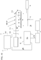
- a configuration of an abnormality determination system 1 for a photovoltaic module M according to a second embodiment will be described with reference to Fig. 10 .
- the abnormality determination system 1 for the photovoltaic module M according to the second embodiment has the same configuration as the abnormality determination system 1 for the photovoltaic module M according to the first embodiment except for points to be described below. Accordingly, in the abnormality determination system 1 for the photovoltaic module M according to the second embodiment, it is possible to obtain the same advantageous effects as those of the abnormality determination system 1 for the photovoltaic module M according to the first embodiment except for the points to be described below.
- Fig. 10 is a diagram showing an example of the configuration of the abnormality determination system 1 for the photovoltaic module M according to the second embodiment.
- the abnormality determination system 1 further includes a clamp sensor 15 that detects a power current of the photovoltaic module M.
- the power output voltage Vo of the photovoltaic module M is input as the input signal to the lock-in amplifier 12a.
- the power current of the photovoltaic module M is detected by the clamp sensor 15.
- An output signal Co from the clamp sensor 15 is input as a signal indicating the power output of the photovoltaic module M to the lock-in amplifier 12a.
- the reference signal RS output from the chopper control unit 113 is input to the lock-in amplifier 12a.
- the lock-in amplifier 12a outputs the signal LAo in accordance with a state of the photovoltaic cell C3.
- the reference signal RS input to the lock-in amplifier 12a indicates a phase (frequency) of the modulated light ML radiated from the modulated light radiation unit 11 to the photovoltaic cell C3.
- the signal LAo output from the lock-in amplifier 12a indicates a state of the photovoltaic cell C3 to which the modulated light ML is radiated.
- the abnormality determination system 1 for the photovoltaic module M further includes the clamp sensor 15 that detects a power current of the photovoltaic module M.
- a signal indicating a power output of the photovoltaic module M input to the lock-in amplifier 12a is an output signal Co from the clamp sensor 15.
- the power output voltage Vo of the photovoltaic module M is not input directly to the lock-in amplifier 12a, but the output signal Co from the clamp sensor 15 detecting the power current of the photovoltaic module M is input to the lock-in amplifier 12a.
- the abnormality determination system 1 for the photovoltaic module M even when the power output voltage Vo of the photovoltaic module M is high, the signal indicating the power output of the photovoltaic module M can be input to the lock-in amplifier 12a. As a result, even when the power output voltage Vo of the photovoltaic module M is high, the determination unit 13 can determine whether the photovoltaic cell C3 is in the abnormal state according to the output signal LAo from the lock-in amplifier 12a.
- the second embodiment conforms to an operation principle according to Expression (3-2) representing a minute change ⁇ I of the current I flowing in the photovoltaic module M and the load resistor R in ⁇ Analytic theory>.
- a configuration of an abnormality determination system 1 for a photovoltaic module M according to a third embodiment will be described with reference to Fig. 11 .
- the abnormality determination system 1 for the photovoltaic module M according to the third embodiment has the same configuration as the abnormality determination system 1 for the photovoltaic module M according to the first embodiment except for points to be described below. Accordingly, in the abnormality determination system 1 for the photovoltaic module M according to the third embodiment, it is possible to obtain the same advantageous effects as those of the abnormality determination system 1 for the photovoltaic module M according to the first embodiment except for the points to be described below.
- Fig. 11 is a diagram showing an example of the configuration of the abnormality determination system 1 for the photovoltaic module M according to the third embodiment.
- the abnormality determination system 1 is applied to a photovoltaic panel array A that includes the photovoltaic module M.
- the photovoltaic module M includes the plurality of photovoltaic cells C1, C2, C3, C4, and C5 connected in series as in the example shown in Fig. 1 .
- the photovoltaic panel array A includes four photovoltaic panels P1, P2, P3, and P4.
- the photovoltaic panel P1 includes the above-described photovoltaic module M and a plurality of photovoltaic modules having the same configuration as the photovoltaic module M.
- the photovoltaic panel P2 includes a plurality of photovoltaic modules having the same configuration as the photovoltaic module M.
- the photovoltaic panels P3 and P4 have the same configuration as the photovoltaic panel P2.
- the photovoltaic panel array A includes many photovoltaic cells C1, C2, C3, C4, C5, and the like connected in series. That is, the many photovoltaic cells C1, C2, C3, C4, C5, and the like included in the photovoltaic panel P1, many photovoltaic cells included in the photovoltaic panel P2, many photovoltaic cells included in the photovoltaic panel P3, and many photovoltaic cells included in the photovoltaic panel P4 are connected in series.
- the photovoltaic panel array A is connected to a power conditioner PC.
- the power conditioner PC converts direct-current power generated by the photovoltaic panel array A into alternating-current power.
- the photovoltaic panel array A includes four photovoltaic panels P1, P2, P3, and P4.
- the photovoltaic panel array A may include any number of photovoltaic panels other than four.
- the abnormality determination system 1 includes the modulated light radiation unit 11, the phase detection unit 12, the determination unit 13, the output unit 14, the clamp sensor 15, a communication control unit 16, and a communication control unit 17.
- the clamp sensor 15 detects a power current of the photovoltaic panel array A.
- the modulated light radiation unit 11 is mounted on an unmanned flying body DR.
- the modulated light ML reflected from the reflector 114 of the modulated light radiation unit 11 mounted on the unmanned flying body DR is radiated to the photovoltaic cell C3.
- the reflector 114 may be omitted and the modulated light ML transmitting through the filter 115 of the modulated light radiation unit 11 may be radiated directly to the photovoltaic cell C3.
- the modulated light radiation unit 11 mounted on the unmanned flying body DR radiates the modulated light ML to one photovoltaic cell C3 among the many photovoltaic cells C1, C2, C3, C4, C5, and the like included in the photovoltaic panel array A.
- the communication control unit 17 connected to the chopper control unit 113 of the modulated light radiation unit 11 is mounted on the unmanned flying body DR.
- the communication control unit 16 is connected to the lock-in amplifier 12a.
- the reference signal RS output from the chopper control unit 113 is input to the lock-in amplifier 12a via the communication control unit 17, wireless communication, and the communication control unit 16.
- the chopper control unit 113 may not be mounted on the unmanned flying body DR and may be mounted near the lock-in amplifier 12a to control the light chopper unit 112 via wireless communication and the communication control unit 17 from the communication control unit 16.
- the abnormality determination system 1 determines that the process shown in Fig. 9 ends.
- the photovoltaic cell to which the modulated light ML has not been radiated remains among the many photovoltaic cells C1, C2, C3, C4, C5, and the like included in the photovoltaic panel array A, in step S5, the abnormality determination system 1 determines that the process shown in Fig. 9 does not end, and then the process returns to step S1.
- the modulated light radiation unit 11 is mounted on the unmanned flying body DR. Therefore, for example, even when the photovoltaic cell C3 is disposed at a high position, the determination unit 13 can determine whether the photovoltaic cell C3 is in an abnormal state.
- the entirety of the abnormality determination system 1 may be realized by dedicated hardware or may be realized by a memory and a microprocessor.
- the abnormality determination system 1 may include a memory and a central processing unit (CPU) and a program for realizing a function of each unit included in each system may be loaded and executed on the memory to realize the function.
- CPU central processing unit
- each unit may be performed by recording a program for realizing some or all of the functions of the abnormality determination system 1 on a computer-readable recording medium and reading and executing the program recoded on the recording medium in the computer system.
- the "computer system” mentioned here is assumed to include an OS or hardware such as peripheral devices.
- the "computer system” is assumed to include a home page supply environment (or a display environment) when a WWW system is used.
- the "computer-readable recording medium” is a flexible disc, a magneto-optical disc, a ROM, a portable medium such as a CD-ROM, or a storage device such as a hard disk contained in the computer system.
- the "computer-readable recording medium” is assumed to retain a program dynamically in a short time like a communication line when a program is transmitted via a communication line such as a telephone circuit or a network such as the Internet and is assumed to retain a program for a given time like a volatile memory inside the computer system serving a server or a client in this case.
- the program may realize some of the above-described functions or may realize the above-described functions in combination with a program previously recorded on the computer system.
Landscapes
- Photovoltaic Devices (AREA)
Description
- The present invention relates to an abnormality determination system and method for a photovoltaic module.
- In the related art, methods of inspecting photovoltaic modules (photovoltaic panels) including a plurality of photovoltaic cells connected in series are known (for example, see Patent Document 1). The document
US 2015/236642 A1 is relevant prior art. - [Patent Document 1]
Japanese Unexamined Patent Application, First Publication No.2013-131679 - In a photovoltaic module disclosed in
Patent Document 1, when a power current of a cell decreases with failure of the cell, a power current of the entire photovoltaic module also decreases. - Accordingly, it is important to discover which cell has failed in the photovoltaic module. A failed cell shows a decrease in a power current and also shows a reverse voltage and a hot spot state. Therefore, when a cell voltage or cell temperature of an individual photovoltaic cell included in a photovoltaic module is monitored, a failed cell can be discovered.
- However, a photovoltaic module is normally sealed with a resin. Therefore, a cell voltage of an individual photovoltaic cell may not be measured. A cell temperature can be easily observed by an infrared camera, but the cell temperature is strongly influenced by an ambient environment. Therefore, when failure of a cell is determined according to only a cell temperature, precision of determination of whether the cell has failed may be lowered.
- The present invention is devised to solve the foregoing problems and an object of the present invention is to provide an abnormality determination system and method for a photovoltaic module capable of accurately determining which photovoltaic cell is in an abnormal state among a plurality of photovoltaic cells connected in series.
- According to an embodiment of the present invention, there is provided an abnormality determination system for a photovoltaic module as recited in
claim 1 and a corresponding method as recited in claim 6. Further advantageous embodiments are recited in the dependent claims. - According to the present invention, it is possible to provide an abnormality determination system and method for a photovoltaic module capable of accurately determining which photovoltaic cell is in an abnormal state among a plurality of photovoltaic cells connected in series.
-
-
Fig. 1 is a diagram showing an example of a configuration of an abnormality determination system for a photovoltaic module according to a first embodiment. -
Fig. 2 is a diagram showing an example of a configuration of an abnormality determination system for a photovoltaic module according to a first modification example of the first embodiment. -
Fig. 3 is a diagram showing an example of a configuration of an abnormality determination system for a photovoltaic module according to a second modification example of the first embodiment. -
Fig. 4A is an equivalent circuit diagram showing a photovoltaic module and a load resistor shown inFig. 1 . -
Fig. 4B is an equivalent circuit diagram showing a minute change in a current flowing in the photovoltaic module and the load resistor shown inFig. 4A . -
Fig. 5 is a modified diagram of the equivalent circuit diagram shown inFig. 4B . -
Fig. 6 is a diagram showing a correlation between a current output by a photovoltaic cell and a voltage applied to a differential resistor. -
Fig. 7A is an equivalent circuit diagram showing an opened photovoltaic module. -
Fig. 7B is an equivalent circuit diagram showing the opened photovoltaic module shown inFig. 7A and a minute change in a power output voltage. -
Fig. 8 is a diagram showing a result of a demonstration experiment. -
Fig. 9 is a flowchart showing a process performed by the abnormality determination system for the photovoltaic module according to the first embodiment. -
Fig. 10 is a diagram showing an example of a configuration of an abnormality determination system for a photovoltaic module according to a second embodiment. -
Fig. 11 is a diagram showing an example of a configuration of an abnormality determination system for a photovoltaic module according to a third embodiment. - Hereinafter, embodiments of the present invention will be described with reference to the drawings. First, a configuration of an
abnormality determination system 1 for a photovoltaic module M according to a first embodiment will be described with reference toFig. 1 . -
Fig. 1 is a diagram showing an example of the configuration of theabnormality determination system 1 for the photovoltaic module M according to the first embodiment. - In the example shown in
Fig. 1 , theabnormality determination system 1 according to the first embodiment is applied to a photovoltaic module M. The photovoltaic module M includes a plurality of photovoltaic cells C1, C2, C3, C4, and C5 connected in series. The photovoltaic module M is connected to a load resistor R. - In the example shown in
Fig. 1 , the photovoltaic module M includes five photovoltaic cells C1, C2, C3, C4, and C5. In another example, the photovoltaic module M may include any number of plural photovoltaic cells connected in series other than five. - In the example shown in
Fig. 1 , theabnormality determination system 1 includes a modulatedlight radiation unit 11, aphase detection unit 12, adetermination unit 13, and anoutput unit 14. The modulatedlight radiation unit 11 includes alaser radiation unit 111, alight chopper unit 112, achopper control unit 113, areflector 114, and afilter 115. Thelaser radiation unit 111 radiates, for example, a laser such as a He-Ne laser. - In the example shown in
Fig. 1 , as described above, the modulatedlight radiation unit 11 includes thelaser radiation unit 111. However, in another example, the modulatedlight radiation unit 11 may include a radiation unit that radiates light other than a laser. - In the example shown in
Fig. 1 , thelight chopper unit 112 modulates the laser radiated from thelaser radiation unit 111 into modulated light ML with a predetermined phase (frequency). Thechopper control unit 113 controls thelight chopper unit 112. Thechopper control unit 113 outputs a reference signal RS indicating the phase (frequency) of the modulated light ML modulated by thelight chopper unit 112. Thefilter 115 reduces the modulated light ML modulated by thelight chopper unit 112. Thefilter 115 is, for example, a neutral density (ND) filter. Thereflector 114 reflects the modulated light ML reduced by thefilter 115. The modulated light ML reflected by thereflector 114 is radiated to the photovoltaic cell C3. - In the example shown in
Fig. 1 , the modulated light ML reflected by thereflector 114 is radiated to the photovoltaic cell C3. In another example, instead, the modulated light ML reflected by thereflector 114 may be radiated to any of the photovoltaic cells C1, C2, C4, and C5 other than the photovoltaic cell C3. In another example, instead, thereflector 114 may be omitted. - In the example shown in
Fig. 1 , thelight chopper unit 112, thefilter 115, and thereflector 114 are arranged in the order of thelight chopper unit 112, thefilter 115, and thereflector 114 between thelaser radiation unit 111 and the photovoltaic module M. In another example, instead, the order of thelight chopper unit 112, thefilter 115, and thereflector 114 may be set to be different. - As described above, in the
abnormality determination system 1 of the photovoltaic module M according to the first embodiment, the modulatedlight radiation unit 11 radiates the modulated light ML to one photovoltaic cell C3 among the plurality of photovoltaic cells C1, C2, C3, C4, and C5 included in the photovoltaic module M. - In the example shown in
Fig. 1 , thephase detection unit 12 includes a lock-inamplifier 12a. Specifically, thephase detection unit 12 is the lock-inamplifier 12a. - The lock-in
amplifier 12a is connected to the photovoltaic module M. Specifically, a power output voltage Vo of the photovoltaic module M is input as an input signal to the lock-inamplifier 12a. The reference signal RS output from thechopper control unit 113 is input to the lock-inamplifier 12a. The lock-inamplifier 12a outputs a signal LAo in accordance with a state of the photovoltaic cell C3. -
Fig. 2 is a diagram showing an example of a configuration of an abnormality determination system for a photovoltaic module according to a first modification example of the first embodiment. In the first modification example of the configuration of the abnormality determination system for the photovoltaic module according to the first embodiment, a minute resistor r for current detection is connected in series to a circuit connecting the photovoltaic module M and the load resistor R. When the power output voltage Vo of the photovoltaic module M exceeds a voltage upper limit of the input signal of the lock-inamplifier 12a, a voltage applied to the minute resistor r for current detection and set in a range below the voltage upper limit of the input signal of the lock-inamplifier 12a is given as an input signal of the lock-inamplifier 12a. -
Fig. 3 is a diagram showing an example of a configuration of an abnormality determination system for a photovoltaic module according to a second modification example of the first embodiment. In the second modification example of the configuration of the abnormality determination system for the photovoltaic module according to the first embodiment, a capacitor C or a highpass filter (not shown) suppressing the power output voltage Vo which is a direct-current voltage or a bandpass filter (not shown) passing an alternating-current component close to a frequency of the modulated light ML is inserted into a conducting wire of an input signal to the lock-inamplifier 12a. - That is, in the examples shown in
Figs. 1 ,2 , and3 , the reference signal RS input to the lock-inamplifier 12a indicates a phase (frequency) of the modulated light ML radiated from the modulatedlight radiation unit 11 to the photovoltaic cell C3. The signal LAo output from the lock-inamplifier 12a indicates a state of the photovoltaic cell C3 to which the modulated light ML is radiated. - As described above, in the
abnormality determination system 1 for the photovoltaic module M according to the first embodiment, thephase detection unit 12 outputs the signal LAo in accordance with the state of the photovoltaic cell C3 according to a signal indicating a power output of the photovoltaic module M and the reference signal RS indicating the phase (frequency) of the modulated light ML. Specifically, when the signal indicating the power output of the photovoltaic module M and the reference signal RS indicating the phase (frequency) of the modulated light ML are input to thephase detection unit 12, thephase detection unit 12 outputs the signal LAo in accordance with the state of the photovoltaic cell C3. - In the examples shown in
Figs. 1 ,2 , and3 , the signal LAo output from the lock-inamplifier 12a is input to thedetermination unit 13. - In the
abnormality determination system 1 for the photovoltaic module M according to the first embodiment, thedetermination unit 13 determines whether the photovoltaic cell C3 is in an abnormal state according to the signal LAo output from thephase detection unit 12. - In the examples shown in
Figs. 1 ,2 , and3 , a determination result in thedetermination unit 13, that is, whether the photovoltaic cell C3 is in the abnormal state, is output by theoutput unit 14. Theoutput unit 14 includes at least one of a display unit that displays the determination result in thedetermination unit 13, a sound output unit that outputs a sound of the determination result in thedetermination unit 13, and a printing unit that prints the determination result in thedetermination unit 13. A user of theabnormality determination system 1 can ascertain whether the photovoltaic cell C3 is in the abnormal state in accordance with the determination result in thedetermination unit 13 output from theoutput unit 14. -
Fig. 4A is an equivalent circuit diagram showing the photovoltaic module M and the load resistor R shown inFig. 1 . - In the example shown in
Fig. 1 , the five photovoltaic cells C1, C2, C3, C4, and C5 are connected in series, but in an example shown inFig. 4A , n photovoltaic cells C1, ..., Ci, ..., and Cn are connected in series. The photovoltaic cell C1 is expressed by a current source C1-1 outputting a current Iph1 and a diode C1-2. The photovoltaic cell Ci is expressed by a current source Ci-1 outputting a current Iphi and a diode Ci-2. The photovoltaic cell Cn is expressed by a current source Cn-1 outputting a current Iphn and a diode Cn-2. - A current Idi flowing in the diode Ci-2 is expressed by Expression (1) below.
[Math. 1]
- In Expression (1), I denotes a current flowing in the entire photovoltaic module M and the load resistor R. I0i denotes a reverse saturation current of the diode Ci-2 and q denotes an elementary charge.
- Vi denotes a forward voltage of the diode Ci-2, n denotes a diode factor, k denotes a Boltzmann constant, and T denotes an absolute temperature.
- In the example shown in
Fig. 1 , the modulated light ML is radiated from the modulatedlight radiation unit 11 to the photovoltaic cell C3. However, in the example shown inFig. 4A , the modulated light ML is radiated from the modulatedlight radiation unit 11 to the photovoltaic cell Cn. - In the example shown in
Fig. 4A , with radiation of the modulated light ML to the photovoltaic cell Cn, a photocurrent of the photovoltaic cell Cn increases by a minute amount ΔIph. When a variation amount derived by the minute amount ΔIph of each unit of the circuit shown inFig. 4A is obtained by a superimposition principle, the variation amount is as indicated inFig. 4B . -
Fig. 4B is an equivalent circuit diagram showing a minute change ΔI in the current I flowing in the photovoltaic module M and the load resistor R shown inFig. 4A . - In the example shown in
Fig. 4B , the photovoltaic cell C1 is expressed by a differential resistor Rd1. - That is, the current source C1-1 (see
Fig. 4A ) from the photocurrent of the photovoltaic cell C1 is opened and lost. When a change of the photovoltaic cell C1 is assumed to be minute, the diode C1-2 (seeFig. 4A ) of the photovoltaic cell C1 is expressed by the differential resistor Rd1. - Similarly, the photovoltaic cell Ci is expressed by the differential resistor Rd1.
- The photovoltaic cell Cn to which the modulated light ML from the modulated
light radiation unit 11 is radiated is expressed by the current source Cn-1 outputting a minute change ΔIphn of the current and a differential resistor Rdn. - The differential resistor Rdi of the photovoltaic cell Ci is expressed by Expression (2) below.
[Math. 2]
-
Fig. 5 is a modified diagram of the equivalent circuit diagram shown inFig. 4B . - A change Δ Vn of the voltage of the photovoltaic cell Cn is expressed by Expression (3-1) below.
- The minute change ΔI of the current I flowing in the photovoltaic module M and the load resistor R is expressed by Expression (3-2) below.
- A change ΔV of a voltage applied to the load resistor R is expressed by Expression (3-3) below.
[Math. 3]


- As indicated in Expression (3-3), when the change ΔIphn in the current is a constant value, the change ΔV in the voltage is proportional to the differential resistor Rdn.
- The denominator of the right side of Expression (3-3) is a sum of differential resistors of all the photovoltaic cells C1, ..., Ci, ..., Cn. Therefore, when the value of the differential resistor is not changed, the denominator of the right side Expression (3-3) is the same despite occurrence of the change ΔIphn in the current in a certain photovoltaic cell.
- When the change ΔIphn of the photocurrent of the photovoltaic cell Cn is changed with radiation of the modulated light ML from the modulated
light radiation unit 11 to the photovoltaic cell Cn, the change ΔV in the voltage applied to the load resistor R is obtained from the minute change ΔI in the current I flowing in the load resistor R. - In the example shown in
Fig. 1 , the power output voltage Vo of the photovoltaic module M, that is, the voltage applied to the load resistor R, is input as an input signal to the lock-inamplifier 12a. Therefore, the change ΔV in the voltage applied to the load resistor R is obtained by the lock-inamplifier 12a. - As a photocurrent Iphn of the photovoltaic cell Cn of the photovoltaic module M is closer to the current I flowing in the entire photovoltaic module M and the load resistor R, the differential resistor Rdn of the photovoltaic cell Cn is larger. When the photocurrent Iphn of the photovoltaic cell Cn is the minimum, the current I flowing in the entire photovoltaic module M and the load resistor R is equal to the photocurrent Iphn and the differential resistor Rdn of the photovoltaic cell Cn becomes the maximum.
- Here, when a constant minute photocurrent which is equal to the magnitude of the change ΔIphn in the current is generated in sequence in all the photovoltaic cells C1, ..., Ci, ..., and Cn, a change in the differential resistor Rdn by the change ΔIphn of the current is negligible in view of the change ΔV in the voltage applied to the load resistor R, and the change ΔIphn in the current is generated in the photovoltaic cell Cn having the large differential resistor Rdn at the time of Rdn >> Rdi and R (i≠n), the change ΔV in the voltage applied to the load resistor R becomes the maximum.
-
Fig. 6 is a diagram showing a correlation between a current I output by the photovoltaic cell Ci in which incident sunlight is constant, that is, the photovoltaic cell Ci in which a current output by the current source Iphi is constant, and a voltage applied to the photovoltaic cell Ci, that is, a voltage applied to the differential resistor Rdi. - In
Fig. 6 , the horizontal axis represents a voltage applied to the differential resistor Rdi. The vertical axis represents the current I output by the photovoltaic cell Ci. As shown inFig. 6 , the voltage applied to the differential resistor Rdi increases as the current I output by the photovoltaic cell Ci decreases. As shown inFig. 6 , when the current I output by the photovoltaic cell Ci is large and the voltage applied to the differential resistor Rdi is small, the differential resistor Rdi increases. Conversely, when the current I output by the photovoltaic cell Ci is small and the voltage applied to the differential resistor Rdi is large, the differential resistor Rdi decreases. -
Fig. 7A is an equivalent circuit diagram showing the opened photovoltaic module M.Fig. 7B is an equivalent circuit diagram showing the opened photovoltaic module M shown inFig. 7A and a minute change ΔV in the power output voltage Vo. - In the examples shown in
Figs. 4A and 4B , the photovoltaic module M is not opened. In the examples shown inFigs. 7A and 7B , however, the photovoltaic module M is opened. - In the examples shown in
Figs. 7A and 7B , the minute change ΔVn in the voltage is made in only the photovoltaic cell Cn in which the minute change ΔIphn of the current is made. Therefore, a minute change ΔV of the power output voltage Vo of the photovoltaic module M is expressed by Expression (4) below.
- Even when a control current source causes a current with a constant value to flow, the minute change ΔI in the current I flowing in the photovoltaic module M and the load resistor R is zero. Therefore, the minute change ΔV of the power output voltage Vo of the photovoltaic module M in this case is also expressed by Expression (4) above.
- As described above, it is considered that a weak component synchronized with the modulated light ML is included in the power output voltage Vo of the photovoltaic module M output to the lock-in
amplifier 12a when the weak modulated light ML is radiated to only the photovoltaic cell Cn in the photovoltaic module M during generation. The weak component is considered to have information in which a state (for example, an operation point of the photovoltaic cell Cn, whether the photovoltaic cell Cn fails) of the photovoltaic cell Cn to which the weak modulated light ML is radiated is reflected. - Accordingly, in the example which is shown in
Fig. 1 and in which theabnormality determination system 1 of the photovoltaic module M according to the first embodiment is applied, as described above, the power output voltage Vo of the photovoltaic module M and the reference signal RS indicating the phase (frequency) of the modulated light ML radiated to the photovoltaic cell C3 are input to the lock-inamplifier 12a. The lock-inamplifier 12a extracts a weak component synchronized with the modulated light ML. The lock-inamplifier 12a outputs the signal LAo in accordance with the state of the photovoltaic cell C3 to thedetermination unit 13. Therefore, in the example shown inFig. 1 , information regarding the state of the photovoltaic cell C3 can be obtained quantitatively and thedetermination unit 13 can determine whether the photovoltaic cell C3 is in an abnormal state. - The present inventors carried out an experiment in which an output voltage of the lock-in
amplifier 12a in the case of radiation of the modulated light ML to the photovoltaic cell which is in an abnormal state (that is, failure) was compared to an output voltage of the lock-inamplifier 12a in the case of radiation of the modulated light ML to the photovoltaic cell which is not in an abnormal state (that is, non-failure). - In the experiment, as in the example shown in
Fig. 1 , the photovoltaic module M including five photovoltaic cells C1, C2, C3, C4, and C5 connected in series was used. The photovoltaic cell C5 or the photovoltaic cell C1 was set to an abnormal state (that is, a state in which normal generation was not possible) by masking the photovoltaic cell C5 or the photovoltaic cell C1. The photovoltaic cells C2, C3, and C4 were set to a normal state (that is, a state in which normal generation was possible) by not masking the photovoltaic cells C2, C3, and C4. - In the experiment, as in the example shown in
Fig. 1 , the power output voltage Vo of the photovoltaic module M was measured. As in the example shown inFig. 1 , the power output voltage Vo was input as an input signal to the lock-inamplifier 12a. In the experiment, unlike the example shown inFig. 1 , a voltage of each of the photovoltaic cells C1, C2, C3, C4, and C5 was measured. - In the experiment, the modulated
light radiation unit 11 was configured as in the example shown inFig. 1 . In the experiment, unlike the example shown inFig. 1 , an LED was used to radiate light simulated sunlight to the photovoltaic cells C1, C2, C3, C4, and C5 rather than sunlight. -
Fig. 8 is a diagram showing a result of a demonstration experiment. - In
Fig. 8 , "cell 1" refers to the photovoltaic cell C1, "cell 2" refers to the photovoltaic cell C2, "cell 3" refers to the photovoltaic cell C3, "cell 4" refers to the photovoltaic cell C4, and "cell 5" refers to the photovoltaic cell C5. - The "average of voltages (V)" of "
cell 1" refers to a voltage (V) of the photovoltaic cell C1, the "average of voltages (V)" of "cell 2" refers to a voltage (V) of the photovoltaic cell C2, the "average of voltages (V)" of "cell 3" refers to a voltage (V) of the photovoltaic cell C3, the "average of voltages (V)" of "cell 4" refers to a voltage (V) of the photovoltaic cell C4, and the "average of voltages (V)" of "cell 5" refers to a voltage (V) of the photovoltaic cell C5. - The "average of voltages (V)" of a "module" refers to a power output voltage Vo (V) of the photovoltaic module M configured by connecting the photovoltaic cells C1, C2, C3, C4, and C5 in series. The "average of voltages (V)" of a "lock-in amplifier" refers to a voltage (V) of the signal LAo output from the lock-in
amplifier 12a when the power output voltage Vo of the photovoltaic module M and the reference signal RS indicating the phase (frequency) of the modulated light ML are input to the lock-inamplifier 12a. - In the demonstration experiment,
condition 1,condition 2, andcondition 3 were set. - In
condition 1, none of the photovoltaic cells C1, C2, C3, C4, and C5 were masked. That is, a normal state was set in all of the photovoltaic cells C1, C2, C3, C4, and C5. Simulated sunlight was radiated to all of the photovoltaic cells C1, C2, C3, C4, and C5. The modulated light ML was radiated from the modulatedlight radiation unit 11 to only the photovoltaic cell C5. - As shown in
Fig. 8 , in "condition 1," the power output voltage Vo of the photovoltaic module M became 1.368 (V). The output voltage of the lock-inamplifier 12a became 0.085 (V). The voltage of the photovoltaic cell C5 in the normal state belongs to a group in which the voltage is higher among the voltages of the other photovoltaic cells C1 to C4 according tocondition 1 ofFig. 8 , and thus a differential resistor Rd5 of the photovoltaic cell C5 belongs to a group in which the differential resistance is smaller. When the differential resistance is small, the change ΔV in the voltage applied to the load resistor R decreases from Expression (3-3). Therefore, the output voltage of the lock-inamplifier 12a decreases. - In
condition 2, the photovoltaic cell C5 was masked without masking the photovoltaic cells C1, C2, C3, and C4. That is, a normal state was set in the photovoltaic cells C1, C2, C3, and C4 and an abnormal state was set in the photovoltaic cell C5. Simulated sunlight was radiated to all of the photovoltaic cells C1, C2, C3, C4, and C5. The modulated light ML was radiated to only the photovoltaic cell C5 set to the abnormal state. - As shown in
Fig. 8 , in "condition 2," the power output voltage Vo of the photovoltaic module M became 1.276 (V). The output voltage of the lock-inamplifier 12a became 3.590 (V). The voltage of the photovoltaic cell C5 in the abnormal state is the smallest in comparison with the voltages of the other photovoltaic cells C1 to C4 according tocondition 2 ofFig. 8 , and thus the differential resistor Rd5 of the photovoltaic cell C5 becomes the largest. When the differential resistance is large, the change ΔV in the voltage applied to the load resistor R increases from Expression (3-3). Therefore, the output voltage of the lock-inamplifier 12a increases. - That is, in
condition 2 in which the photovoltaic cell C5 was set to the abnormal state, the power amount of the entire photovoltaic module M was lowered and the power output voltage Vo of the photovoltaic module M was lowered than incondition 1 in which all of the photovoltaic cells C1, C2, C3, C4, and C5 were set to the normal state. - Conversely, in
condition 2 in which the modulated light ML was radiated to the photovoltaic cell C5 set to the abnormal state, the output voltage of the lock-inamplifier 12a was raised further than incondition 1 in which the modulated light ML was radiated to the photovoltaic cell C5 set to the normal state. - In
condition 3, the photovoltaic cell C1 was masked without masking the photovoltaic cells C2, C3, C4, and C5. That is, a normal state was set in the photovoltaic cells C2, C3, C4, and C5 and an abnormal state was set in the photovoltaic cell C1. Simulated sunlight was radiated to all of the photovoltaic cells C1, C2, C3, C4, and C5. The modulated light ML was radiated to only the photovoltaic cell C5 set to the normal state. - As shown in
Fig. 8 , in "condition 3," the power output voltage Vo of the photovoltaic module M became 1.075 (V). The output voltage of the lock-inamplifier 12a became 0.037 (V). The voltage of the photovoltaic cell C5 in the normal state belongs to a group in which the voltage is higher among the voltages of the other photovoltaic cells C1 to C4 according tocondition 3 ofFig. 8 , and thus the differential resistor Rd5 of the photovoltaic cell C5 belongs to a group in which the differential resistance is smaller. When the differential resistance is small, the change ΔV in the voltage applied to the load resistor R decreases from Expression (3-3). Therefore, the output voltage of the lock-inamplifier 12a decreases. - That is, in
condition 3 in which the photovoltaic cell C1 was set to the abnormal state, the power amount of the entire photovoltaic module M was lowered and the power output voltage Vo of the photovoltaic module M was lowered than incondition 1 in which all of the photovoltaic cells C1, C2, C3, C4, and C5 were set to the normal state. - Conversely, in
condition 3 in which the modulated light ML was radiated to the photovoltaic cell C5 set to the normal state, the output voltage of the lock-inamplifier 12a became almost equal to that ofcondition 1 in which the modulated light ML was radiated to the photovoltaic cell C5 set to the normal state. - That is, in the demonstration experiment, the present inventors found that when the modulated light ML was radiated to the photovoltaic cell in the abnormal state, the output voltage of the lock-in
amplifier 12a was higher than the output voltage of the lock-inamplifier 12a when the modulated light ML was radiated to the photovoltaic cell in the normal state. - That is, in the demonstration experiment, the present inventors found that when the photovoltaic cell to which the modulated light ML was radiated was in the abnormal state, the lock-in
amplifier 12a output a higher voltage than when the photovoltaic cell to which the modulated light ML was radiated was in the normal state. - In the example shown in
Fig. 8 , the present inventors found that whether the photovoltaic cell to which the modulated light ML was radiated was in the abnormal state was determined according to the output voltage of the lock-inamplifier 12a by setting a threshold voltage of the output voltage of the lock-inamplifier 12a to, for example, 2.000 (V). - Specifically, in
condition 1, since the output voltage (0.085 (V)) of the lock-inamplifier 12a is equal to or less than the threshold voltage (2.000 (V)), it is possible to determine that the photovoltaic cell C5 to which the modulated light ML is radiated is in the normal state. Incondition 2, since the output voltage (3.590 (V)) of the lock-inamplifier 12a is higher than the threshold voltage (2.000 (V)), it is possible to determine that the photovoltaic cell C5 to which the modulated light ML is radiated is in the abnormal state. Incondition 3, since the output voltage (0.037 (V)) of the lock-inamplifier 12a is equal to or less than the threshold voltage (2.000 (V)), it is possible to determine that the photovoltaic cell C5 to which the modulated light ML is radiated is in the normal state. -
Fig. 9 is a flowchart showing a process performed by theabnormality determination system 1 for the photovoltaic module M according to the first embodiment. - In step S1, the modulated
light radiation unit 11 radiates the modulated light ML to one photovoltaic cell C1 among the plurality of photovoltaic cells C1, C2, C3, C4, and C5 included in the photovoltaic module M. - Subsequently, in step S2, the power output voltage Vo of the photovoltaic module M is input as a signal indicating the power output of the photovoltaic module M to the lock-in
amplifier 12a included in thephase detection unit 12. The reference signal RS indicating the phase (frequency) of the modulated light ML is input from thechopper control unit 113 of the modulatedlight radiation unit 11 to the lock-inamplifier 12a. The lock-inamplifier 12a extracts a weak component synchronized with the modulated light ML and outputs the signal LAo in accordance with the state of the photovoltaic cell C1 to thedetermination unit 13. - Subsequently, in step S3, the
determination unit 13 determines whether the photovoltaic cell C1 is in the abnormal state according to the output signal LAo from the lock-inamplifier 12a of thephase detection unit 12. - In the example in which the
abnormality determination system 1 for the photovoltaic module M according to the first embodiment is applied, when a value indicated by the output signal LAo from the lock-inamplifier 12a of thephase detection unit 12 is greater than a threshold, thedetermination unit 13 determines in step S3 that the photovoltaic cell C1 to which the modulated light ML is radiated is in the abnormal state. Conversely, when the value indicated by the output signal LAo from the lock-inamplifier 12a of thephase detection unit 12 is equal to or less than the threshold, thedetermination unit 13 determines in step S3 that the photovoltaic cell C1 to which the modulated light ML is radiated is in the normal state. - In the example which is shown in
Fig. 8 and to which theabnormality determination system 1 of the photovoltaic module M according to the first embodiment is applied, for example, when the output voltage of the lock-inamplifier 12a is greater than the threshold voltage of 2.000 (V), thedetermination unit 13 determines in step S3 that the photovoltaic cell C1 to which the modulated light ML is radiated is in the abnormal state. Conversely, for example, when the output voltage of the lock-inamplifier 12a is equal to or less than the threshold voltage of 2.000 (V), thedetermination unit 13 determines in step S3 that the photovoltaic cell C1 to which the modulated light ML is radiated is in the normal state. - Subsequently, in step S4, the
output unit 14 outputs a determination result by thedetermination unit 13, that is, whether the photovoltaic cell C1 to which the modulated light ML is radiated is in the abnormal state. - Subsequently, in step S5, the
abnormality determination system 1 determines whether the process shown inFig. 9 ends. When the modulated light ML is radiated to all of the plurality of photovoltaic cells C1, C2, C3, C4, and C5 included in the photovoltaic module M, theabnormality determination system 1 determines in step S5 that the process shown inFig. 9 ends. When the photovoltaic cell to which the modulated light ML is not radiated remains among the plurality of photovoltaic cells C1, C2, C3, C4, and C5 included in the photovoltaic module M, theabnormality determination system 1 determines in step S5 that the process shown inFig. 9 does not end and the process returns to step S1. - In step S1, the modulated
light radiation unit 11 radiates the modulated light ML to the subsequent photovoltaic cell C2 among the plurality of photovoltaic cells C1, C2, C3, C4, and C5 included in the photovoltaic module M. - The
abnormality determination system 1 repeatedly performs the processes of steps S1 to S4 described above until the abnormality determination of all the plurality of photovoltaic cells C1, C2, C3, C4, and C5 included in the photovoltaic module M is completed. - In the above-described example, the determination result in step S4 is output whenever the abnormality determination of step S3 in each of the photovoltaic cells C1, C2, C3, C4, and C5 is performed. In another example, however, the
output unit 14 may instead summarize and output the determination result of step S3 in each of the photovoltaic cells C1, C2, C3, C4, and C5. - The
abnormality determination system 1 for the photovoltaic module M according to the first embodiment has been described above. - The
abnormality determination system 1 for the photovoltaic module M according to the first embodiment is theabnormality determination system 1 for the photovoltaic module M including the plurality of photovoltaic cells C1, C2, C3, C4, and C5 connected in series. Theabnormality determination system 1 includes the modulatedlight radiation unit 11 configured to radiate the modulated light ML to one photovoltaic cell C3 among the plurality of photovoltaic cells C1, C2, C3, C4, and C5; thephase detection unit 12 configured to output the signal LAo in accordance with a state of the photovoltaic cell C3 according to the signal indicating a power output of the photovoltaic module M and the reference signal RS indicating a phase (frequency) of the modulated light ML; and thedetermination unit 13 configured to determine whether the photovoltaic cell C3 is in an abnormal state according to the signal LAo output from thephase detection unit 12. - In the
abnormality determination system 1 for the photovoltaic module M according to the first embodiment, thedetermination unit 13 determines whether the photovoltaic cell C3 is in the abnormal state according to a value indicated by the signal LAo output from thephase detection unit 12 and a threshold. - With such a configuration, the
determination unit 13 can accurately determine which photovoltaic cell is in the abnormal state among the plurality of photovoltaic cells C1, C2, C3, C4, and C5 connected in series. - In an example to which the
abnormality determination system 1 for the photovoltaic module M according to the first embodiment is applied, thephase detection unit 12 is the lock-inamplifier 12a. The signal indicating the power output of the photovoltaic module M and the reference signal RS are input to the lock-inamplifier 12a. When the photovoltaic cell C3 to which the modulated light ML is radiated is in the abnormal state, the lock-inamplifier 12a outputs a voltage higher than a voltage output from the lock-inamplifier 12a when the photovoltaic cell C3 to which the modulated light ML is radiated is in the normal state. Thedetermination unit 13 determines that the photovoltaic cell C3 to which the modulated light ML is radiated is in the abnormal state when an output voltage of the lock-inamplifier 12a is higher than a threshold voltage. Thedetermination unit 13 determines that the photovoltaic cell C3 to which the modulated light ML is radiated is in the normal state when the output voltage of the lock-inamplifier 12a is equal to or less than the threshold voltage. - With such a configuration, the
phase detection unit 12 can extract a weak component synchronized with the phase (frequency) of the modulated light ML from the signal indicating the power output of the photovoltaic module M with high precision. - A configuration of an
abnormality determination system 1 for a photovoltaic module M according to a second embodiment will be described with reference toFig. 10 . Theabnormality determination system 1 for the photovoltaic module M according to the second embodiment has the same configuration as theabnormality determination system 1 for the photovoltaic module M according to the first embodiment except for points to be described below. Accordingly, in theabnormality determination system 1 for the photovoltaic module M according to the second embodiment, it is possible to obtain the same advantageous effects as those of theabnormality determination system 1 for the photovoltaic module M according to the first embodiment except for the points to be described below. -
Fig. 10 is a diagram showing an example of the configuration of theabnormality determination system 1 for the photovoltaic module M according to the second embodiment. - In an example which is shown in
Fig. 10 and to which theabnormality determination system 1 for the photovoltaic module M according to the second embodiment is applied, theabnormality determination system 1 further includes aclamp sensor 15 that detects a power current of the photovoltaic module M. - As described above, in the example shown in
Fig. 1 , the power output voltage Vo of the photovoltaic module M is input as the input signal to the lock-inamplifier 12a. - In the example shown in
Fig. 10 , instead, the power current of the photovoltaic module M is detected by theclamp sensor 15. An output signal Co from theclamp sensor 15 is input as a signal indicating the power output of the photovoltaic module M to the lock-inamplifier 12a. - In the example shown in
Fig. 10 , as in the example shown inFig. 1 , the reference signal RS output from thechopper control unit 113 is input to the lock-inamplifier 12a. The lock-inamplifier 12a outputs the signal LAo in accordance with a state of the photovoltaic cell C3. - That is, in the example shown in
Fig. 10 , as in the example shown inFig. 1 , the reference signal RS input to the lock-inamplifier 12a indicates a phase (frequency) of the modulated light ML radiated from the modulatedlight radiation unit 11 to the photovoltaic cell C3. The signal LAo output from the lock-inamplifier 12a indicates a state of the photovoltaic cell C3 to which the modulated light ML is radiated. - The
abnormality determination system 1 for the photovoltaic module M according to the second embodiment further includes theclamp sensor 15 that detects a power current of the photovoltaic module M. - In the
abnormality determination system 1 for the photovoltaic module M according to the second embodiment, a signal indicating a power output of the photovoltaic module M input to the lock-inamplifier 12a is an output signal Co from theclamp sensor 15. - That is, in the
abnormality determination system 1 for the photovoltaic module M according to the second embodiment, the power output voltage Vo of the photovoltaic module M is not input directly to the lock-inamplifier 12a, but the output signal Co from theclamp sensor 15 detecting the power current of the photovoltaic module M is input to the lock-inamplifier 12a. - Therefore, in the
abnormality determination system 1 for the photovoltaic module M according to the second embodiment, even when the power output voltage Vo of the photovoltaic module M is high, the signal indicating the power output of the photovoltaic module M can be input to the lock-inamplifier 12a. As a result, even when the power output voltage Vo of the photovoltaic module M is high, thedetermination unit 13 can determine whether the photovoltaic cell C3 is in the abnormal state according to the output signal LAo from the lock-inamplifier 12a. The second embodiment conforms to an operation principle according to Expression (3-2) representing a minute change ΔI of the current I flowing in the photovoltaic module M and the load resistor R in <Analytic theory>. - A configuration of an
abnormality determination system 1 for a photovoltaic module M according to a third embodiment will be described with reference toFig. 11 . Theabnormality determination system 1 for the photovoltaic module M according to the third embodiment has the same configuration as theabnormality determination system 1 for the photovoltaic module M according to the first embodiment except for points to be described below. Accordingly, in theabnormality determination system 1 for the photovoltaic module M according to the third embodiment, it is possible to obtain the same advantageous effects as those of theabnormality determination system 1 for the photovoltaic module M according to the first embodiment except for the points to be described below. -
Fig. 11 is a diagram showing an example of the configuration of theabnormality determination system 1 for the photovoltaic module M according to the third embodiment. - In an example shown in
Fig. 11 , theabnormality determination system 1 according to the third embodiment is applied to a photovoltaic panel array A that includes the photovoltaic module M. The photovoltaic module M includes the plurality of photovoltaic cells C1, C2, C3, C4, and C5 connected in series as in the example shown inFig. 1 . - In the example shown in
Fig. 11 , the photovoltaic panel array A includes four photovoltaic panels P1, P2, P3, and P4. The photovoltaic panel P1 includes the above-described photovoltaic module M and a plurality of photovoltaic modules having the same configuration as the photovoltaic module M. The photovoltaic panel P2 includes a plurality of photovoltaic modules having the same configuration as the photovoltaic module M. The photovoltaic panels P3 and P4 have the same configuration as the photovoltaic panel P2. - In the example shown in
Fig. 11 , the photovoltaic panel array A includes many photovoltaic cells C1, C2, C3, C4, C5, and the like connected in series. That is, the many photovoltaic cells C1, C2, C3, C4, C5, and the like included in the photovoltaic panel P1, many photovoltaic cells included in the photovoltaic panel P2, many photovoltaic cells included in the photovoltaic panel P3, and many photovoltaic cells included in the photovoltaic panel P4 are connected in series. The photovoltaic panel array A is connected to a power conditioner PC. The power conditioner PC converts direct-current power generated by the photovoltaic panel array A into alternating-current power. - As described above, in the example shown in
Fig. 11 , the photovoltaic panel array A includes four photovoltaic panels P1, P2, P3, and P4. In another example, the photovoltaic panel array A may include any number of photovoltaic panels other than four. - In the example which is shown in
Fig. 11 and to which theabnormality determination system 1 for the photovoltaic module M according to the third embodiment is applied, theabnormality determination system 1 includes the modulatedlight radiation unit 11, thephase detection unit 12, thedetermination unit 13, theoutput unit 14, theclamp sensor 15, acommunication control unit 16, and acommunication control unit 17. Theclamp sensor 15 detects a power current of the photovoltaic panel array A. The modulatedlight radiation unit 11 is mounted on an unmanned flying body DR. - In the example shown in
Fig. 11 , the modulated light ML reflected from thereflector 114 of the modulatedlight radiation unit 11 mounted on the unmanned flying body DR is radiated to the photovoltaic cell C3. However, in another example, instead, thereflector 114 may be omitted and the modulated light ML transmitting through thefilter 115 of the modulatedlight radiation unit 11 may be radiated directly to the photovoltaic cell C3. - As described above, in the
abnormality determination system 1 for the photovoltaic module M according to the third embodiment, the modulatedlight radiation unit 11 mounted on the unmanned flying body DR radiates the modulated light ML to one photovoltaic cell C3 among the many photovoltaic cells C1, C2, C3, C4, C5, and the like included in the photovoltaic panel array A. - In the example shown in
Fig. 11 , thecommunication control unit 17 connected to thechopper control unit 113 of the modulatedlight radiation unit 11 is mounted on the unmanned flying body DR. Thecommunication control unit 16 is connected to the lock-inamplifier 12a. The reference signal RS output from thechopper control unit 113 is input to the lock-inamplifier 12a via thecommunication control unit 17, wireless communication, and thecommunication control unit 16. As another example, thechopper control unit 113 may not be mounted on the unmanned flying body DR and may be mounted near the lock-inamplifier 12a to control thelight chopper unit 112 via wireless communication and thecommunication control unit 17 from thecommunication control unit 16. - In an example to which the
abnormality determination system 1 for the photovoltaic module M according to the third embodiment is applied, when the modulated light ML is radiated to all of the many photovoltaic cells C1, C2, C3, C4, C5, and the like included in the photovoltaic panel array A, in step S5 ofFig. 9 , theabnormality determination system 1 determines that the process shown inFig. 9 ends. When the photovoltaic cell to which the modulated light ML has not been radiated remains among the many photovoltaic cells C1, C2, C3, C4, C5, and the like included in the photovoltaic panel array A, in step S5, theabnormality determination system 1 determines that the process shown inFig. 9 does not end, and then the process returns to step S1. - As described above, in the
abnormality determination system 1 for the photovoltaic module M according to the third embodiment, the modulatedlight radiation unit 11 is mounted on the unmanned flying body DR. Therefore, for example, even when the photovoltaic cell C3 is disposed at a high position, thedetermination unit 13 can determine whether the photovoltaic cell C3 is in an abnormal state. - The embodiments of the present invention have been described in detail above with reference to the drawings, but specific configurations are not limited to the embodiments and may be appropriately modified within the scope of the present invention without departing from the gist of the present invention. The configurations described in the above-described embodiments may be combined.
- Apart or the entirety of the
abnormality determination system 1 according to the foregoing embodiments may be realized by dedicated hardware or may be realized by a memory and a microprocessor. - Apart or the entirety of the
abnormality determination system 1 may include a memory and a central processing unit (CPU) and a program for realizing a function of each unit included in each system may be loaded and executed on the memory to realize the function. - The process of each unit may be performed by recording a program for realizing some or all of the functions of the
abnormality determination system 1 on a computer-readable recording medium and reading and executing the program recoded on the recording medium in the computer system. The "computer system" mentioned here is assumed to include an OS or hardware such as peripheral devices. The "computer system" is assumed to include a home page supply environment (or a display environment) when a WWW system is used. - The "computer-readable recording medium" is a flexible disc, a magneto-optical disc, a ROM, a portable medium such as a CD-ROM, or a storage device such as a hard disk contained in the computer system. The "computer-readable recording medium" is assumed to retain a program dynamically in a short time like a communication line when a program is transmitted via a communication line such as a telephone circuit or a network such as the Internet and is assumed to retain a program for a given time like a volatile memory inside the computer system serving a server or a client in this case. The program may realize some of the above-described functions or may realize the above-described functions in combination with a program previously recorded on the computer system.
-
- 1 Abnormality determination system
- 11 Modulated light radiation unit
- 111 Laser radiation unit
- 112 Light chopper unit
- 113 Chopper control unit
- 114 Reflector
- 115 Filter
- 12 Phase detection unit
- 12a Lock-in amplifier
- 13 Determination unit
- 14 Output unit
- 15 Clamp sensor
- 16 Communication control unit
- 17 Communication control unit
- A Photovoltaic panel array
- P1, P2, P3, P4 Photovoltaic panel
- M Photovoltaic module
- C1, C2, C3, C4, C5 Photovoltaic cell
- R Load resistor
- r Minute resistor for current detection
- C Capacitor
- DR Unmanned flying body
- PC Power conditioner
Claims (6)
- An abnormality determination system (1) for a photovoltaic module (M) including a plurality of photovoltaic cells (C1, C2, C3, C4, C5) connected in series, the abnormality determination system (1) for the photovoltaic module (M) comprising:a modulated light radiation unit (11) configured to radiate modulated light to one photovoltaic cell among the plurality of photovoltaic cells (C1, C2, C3, C4, C5);a lock-in amplifier (12a) configured to output a signal in accordance with a state of the one photovoltaic cell according to a signal indicating a power output of the photovoltaic module (M) and a reference signal indicating a phase of the modulated light; anda determination unit (13) configured to determine whether the one photovoltaic cell is in an abnormal state according to the signal output from the lock-in amplifier (12a),characterised in that the signal indicating the power output of the photovoltaic module (M) and the reference signal are input to the lock-in amplifier (12a).
- The abnormality determination system (1) for the photovoltaic module (M) according to claim 1, wherein the determination unit (13) determines whether the one photovoltaic cell is in the abnormal state according to a value indicated by the signal output from the lock-in amplifier (12a) and a threshold.
- The abnormality determination system (1) for the photovoltaic module (M) according to claim 2,
wherein, when the one photovoltaic cell is in the abnormal state, the lock-in amplifier (12a) is configured to output a higher voltage than a voltage output from the lock-in amplifier (12a) when the one photovoltaic cell is in a normal state, and
wherein the determination unit (13) is configured to determine that the one photovoltaic cell is in the abnormal state when an output voltage of the lock-in amplifier (12a) is higher than a threshold voltage, and determine that the one photovoltaic cell is in the normal state when the output voltage of the lock-in amplifier (12a) is equal to or less than the threshold voltage. - The abnormality determination system (1) for the photovoltaic module (M) according to claim 3, further comprising:a clamp sensor (15) configured to detect a power current of the photovoltaic module (M),wherein the signal indicating the power output of the photovoltaic module (M) input to the lock-in amplifier (12a) is a signal output from the clamp sensor (15).
- The abnormality determination system (1) for the photovoltaic module (M) according to claim 1, wherein the modulated light radiation unit (11) is mounted on an unmanned flying body (DR).
- An abnormality determination method for a photovoltaic module (M) including a plurality of photovoltaic cells (C1, C2, C3, C4, C5) connected in series, the abnormality determination method for the photovoltaic module (M) comprising:a first step of radiating modulated light to one photovoltaic cell among the plurality of photovoltaic cells (C1, C2, C3, C4, C5);a second step of outputting a signal in accordance with a state of the one photovoltaic cell from a lock-in amplifier (12a) according to a signal indicating a power output of the photovoltaic module (M) and a reference signal indicating a phase of the modulated light; anda third step of determining whether the one photovoltaic cell is in an abnormal state according to the signal in accordance with the state of the one photovoltaic cell,wherein the signal indicating the power output of the photovoltaic module (M) and the reference signal are input to the lock-in amplifier (12a).
Applications Claiming Priority (2)
| Application Number | Priority Date | Filing Date | Title |
|---|---|---|---|
| JP2017005717 | 2017-01-17 | ||
| PCT/JP2017/041644 WO2018135123A1 (en) | 2017-01-17 | 2017-11-20 | Solar cell module error determination system and method |
Publications (3)
| Publication Number | Publication Date |
|---|---|
| EP3573230A1 EP3573230A1 (en) | 2019-11-27 |
| EP3573230A4 EP3573230A4 (en) | 2020-06-03 |
| EP3573230B1 true EP3573230B1 (en) | 2021-05-26 |
Family
ID=62908706
Family Applications (1)
| Application Number | Title | Priority Date | Filing Date |
|---|---|---|---|
| EP17893323.0A Active EP3573230B1 (en) | 2017-01-17 | 2017-11-20 | Solar cell module error determination system and method |
Country Status (3)
| Country | Link |
|---|---|
| EP (1) | EP3573230B1 (en) |
| JP (1) | JP6712816B2 (en) |
| WO (1) | WO2018135123A1 (en) |
Families Citing this family (3)
| Publication number | Priority date | Publication date | Assignee | Title |
|---|---|---|---|---|
| CN113169710B (en) | 2018-12-13 | 2024-03-08 | 学校法人帝京大学 | Method for estimating operating voltage of solar cell units in solar cell module and system for estimating operating voltage of solar cell units |
| JP7557774B2 (en) * | 2020-12-25 | 2024-09-30 | 学校法人帝京大学 | System and method for determining abnormality of solar cell module |
| JP2023110461A (en) | 2022-01-28 | 2023-08-09 | 学校法人帝京大学 | Abnormality determination system for solar cell module, abnormality determination method and program for solar cell module |
Family Cites Families (9)
| Publication number | Priority date | Publication date | Assignee | Title |
|---|---|---|---|---|
| JP4370391B2 (en) * | 2002-02-08 | 2009-11-25 | 独立行政法人産業技術総合研究所 | Photoelectric conversion characteristic evaluation method and apparatus therefor |
| ZA200905127B (en) | 2007-02-14 | 2010-09-29 | Ericsson Telefon Ab L M | Codeword to layer mapping in a system implementing HARQ |
| JP5134479B2 (en) * | 2008-09-19 | 2013-01-30 | 三菱重工業株式会社 | Inspection device for photoelectric conversion device module |
| JP5423999B2 (en) | 2011-12-22 | 2014-02-19 | パルステック工業株式会社 | Solar panel inspection method |
| CN104184413A (en) * | 2013-05-27 | 2014-12-03 | 新科实业有限公司 | Test method and test device for solar panel |
| JP6395205B2 (en) * | 2014-02-18 | 2018-09-26 | 株式会社Screenホールディングス | Inspection apparatus and inspection method |
| US9641125B2 (en) * | 2015-01-23 | 2017-05-02 | Alliance For Sustainable Energy, Llc | Luminescence imaging systems and methods for evaluating photovoltaic devices |
| WO2017042248A1 (en) * | 2015-09-08 | 2017-03-16 | Danmarks Tekniske Universitet | Method and apparatus for characterization of a solar cell |
| CN105915179A (en) * | 2016-04-12 | 2016-08-31 | 哈尔滨工业大学 | Wafer and solar cell photoinduced carrier radiation phase lock imaging detection method and system |
-
2017
- 2017-11-20 WO PCT/JP2017/041644 patent/WO2018135123A1/en not_active Ceased
- 2017-11-20 JP JP2018562903A patent/JP6712816B2/en active Active
- 2017-11-20 EP EP17893323.0A patent/EP3573230B1/en active Active
Also Published As
| Publication number | Publication date |
|---|---|
| WO2018135123A1 (en) | 2018-07-26 |
| JP6712816B2 (en) | 2020-06-24 |
| EP3573230A4 (en) | 2020-06-03 |
| EP3573230A1 (en) | 2019-11-27 |
| JPWO2018135123A1 (en) | 2019-07-25 |
Similar Documents
| Publication | Publication Date | Title |
|---|---|---|
| US20240248146A1 (en) | Multispectral impedance determination under dynamic load conditions | |
| Momeni et al. | Fault diagnosis in photovoltaic arrays using GBSSL method and proposing a fault correction system | |
| Bovy et al. | Photometric redshifts and quasar probabilities from a single, data-driven generative model | |
| EP3324611B1 (en) | Event-based sensor, user device including the same, and operation method of the same | |
| US20230188091A1 (en) | Method and apparatus for diagnosing photovoltaic panel faults | |
| US9998071B2 (en) | Failure diagnosis method and failure diagnosis system for photovoltaic system | |
| Hanson et al. | Partial-shading assessment of photovoltaic installations via module-level monitoring | |
| US10164457B2 (en) | Charging method and apparatus | |
| KR101369435B1 (en) | Apparatus for evaluating characteristics of solar cell | |
| EP3573230A1 (en) | Solar cell module error determination system and method | |
| JP6474305B2 (en) | Diagnostic method and monitoring device for photovoltaic power generation system | |
| EP2996158A1 (en) | Solar power system, anomaly determination processing device, anomaly determination processing method, and program | |
| US20120239322A1 (en) | Abnormality diagnosis device, method therefor, and computer-readable medium | |
| US10707809B2 (en) | Ground fault detection device | |
| EP3896846B1 (en) | Estimation method for operation voltage of solar battery cell in solar cell module and solar battery cell operation voltage estimation system | |
| EP3324162A1 (en) | Human body detecting device | |
| CN111245364A (en) | Method for determining a corrected current-voltage characteristic curve of an electrical system | |
| CN108983065B (en) | Voltage amplifying circuit, detection circuit and circuit detection method thereof | |
| US20180175791A1 (en) | Apparatus and system for detecting photovoltaic health and quality in solar panels | |
| JP2004247618A (en) | Inspection method of solar cell element | |
| JP2000222052A (en) | Method and apparatus for measuring solar cell output characteristics | |
| Kobayashi | Partial shading method to estimate the shunt resistance component of a photovoltaic cell in a module | |
| US10845238B2 (en) | Circuit and device for small photo currents and detection of small photo currents | |
| JPS599781A (en) | Light position detector | |
| CN110243915B (en) | Electrochemical sensor automatic identification and failure detection system and detection method thereof |
Legal Events
| Date | Code | Title | Description |
|---|---|---|---|
| STAA | Information on the status of an ep patent application or granted ep patent |
Free format text: STATUS: THE INTERNATIONAL PUBLICATION HAS BEEN MADE |
|
| PUAI | Public reference made under article 153(3) epc to a published international application that has entered the european phase |
Free format text: ORIGINAL CODE: 0009012 |
|
| STAA | Information on the status of an ep patent application or granted ep patent |
Free format text: STATUS: REQUEST FOR EXAMINATION WAS MADE |
|
| 17P | Request for examination filed |
Effective date: 20190709 |
|
| AK | Designated contracting states |
Kind code of ref document: A1 Designated state(s): AL AT BE BG CH CY CZ DE DK EE ES FI FR GB GR HR HU IE IS IT LI LT LU LV MC MK MT NL NO PL PT RO RS SE SI SK SM TR |
|
| AX | Request for extension of the european patent |
Extension state: BA ME |
|
| DAV | Request for validation of the european patent (deleted) | ||
| DAX | Request for extension of the european patent (deleted) | ||
| A4 | Supplementary search report drawn up and despatched |
Effective date: 20200506 |
|
| RIC1 | Information provided on ipc code assigned before grant |
Ipc: H02S 10/40 20140101ALI20200428BHEP Ipc: H02S 50/15 20140101AFI20200428BHEP |
|
| GRAP | Despatch of communication of intention to grant a patent |
Free format text: ORIGINAL CODE: EPIDOSNIGR1 |
|
| STAA | Information on the status of an ep patent application or granted ep patent |
Free format text: STATUS: GRANT OF PATENT IS INTENDED |
|
| INTG | Intention to grant announced |
Effective date: 20210208 |
|
| GRAS | Grant fee paid |
Free format text: ORIGINAL CODE: EPIDOSNIGR3 |
|
| GRAA | (expected) grant |
Free format text: ORIGINAL CODE: 0009210 |
|
| STAA | Information on the status of an ep patent application or granted ep patent |
Free format text: STATUS: THE PATENT HAS BEEN GRANTED |
|
| AK | Designated contracting states |
Kind code of ref document: B1 Designated state(s): AL AT BE BG CH CY CZ DE DK EE ES FI FR GB GR HR HU IE IS IT LI LT LU LV MC MK MT NL NO PL PT RO RS SE SI SK SM TR |
|
| REG | Reference to a national code |
Ref country code: GB Ref legal event code: FG4D |
|
| REG | Reference to a national code |
Ref country code: CH Ref legal event code: EP |
|
| REG | Reference to a national code |
Ref country code: AT Ref legal event code: REF Ref document number: 1397254 Country of ref document: AT Kind code of ref document: T Effective date: 20210615 |
|
| REG | Reference to a national code |
Ref country code: DE Ref legal event code: R096 Ref document number: 602017039488 Country of ref document: DE |
|
| REG | Reference to a national code |
Ref country code: IE Ref legal event code: FG4D |
|
| REG | Reference to a national code |
Ref country code: LT Ref legal event code: MG9D |
|
| REG | Reference to a national code |
Ref country code: AT Ref legal event code: MK05 Ref document number: 1397254 Country of ref document: AT Kind code of ref document: T Effective date: 20210526 |
|
| PG25 | Lapsed in a contracting state [announced via postgrant information from national office to epo] |
Ref country code: FI Free format text: LAPSE BECAUSE OF FAILURE TO SUBMIT A TRANSLATION OF THE DESCRIPTION OR TO PAY THE FEE WITHIN THE PRESCRIBED TIME-LIMIT Effective date: 20210526 Ref country code: LT Free format text: LAPSE BECAUSE OF FAILURE TO SUBMIT A TRANSLATION OF THE DESCRIPTION OR TO PAY THE FEE WITHIN THE PRESCRIBED TIME-LIMIT Effective date: 20210526 Ref country code: HR Free format text: LAPSE BECAUSE OF FAILURE TO SUBMIT A TRANSLATION OF THE DESCRIPTION OR TO PAY THE FEE WITHIN THE PRESCRIBED TIME-LIMIT Effective date: 20210526 Ref country code: AT Free format text: LAPSE BECAUSE OF FAILURE TO SUBMIT A TRANSLATION OF THE DESCRIPTION OR TO PAY THE FEE WITHIN THE PRESCRIBED TIME-LIMIT Effective date: 20210526 Ref country code: BG Free format text: LAPSE BECAUSE OF FAILURE TO SUBMIT A TRANSLATION OF THE DESCRIPTION OR TO PAY THE FEE WITHIN THE PRESCRIBED TIME-LIMIT Effective date: 20210826 |
|
| REG | Reference to a national code |
Ref country code: NL Ref legal event code: MP Effective date: 20210526 |
|
| PG25 | Lapsed in a contracting state [announced via postgrant information from national office to epo] |
Ref country code: RS Free format text: LAPSE BECAUSE OF FAILURE TO SUBMIT A TRANSLATION OF THE DESCRIPTION OR TO PAY THE FEE WITHIN THE PRESCRIBED TIME-LIMIT Effective date: 20210526 Ref country code: SE Free format text: LAPSE BECAUSE OF FAILURE TO SUBMIT A TRANSLATION OF THE DESCRIPTION OR TO PAY THE FEE WITHIN THE PRESCRIBED TIME-LIMIT Effective date: 20210526 Ref country code: PT Free format text: LAPSE BECAUSE OF FAILURE TO SUBMIT A TRANSLATION OF THE DESCRIPTION OR TO PAY THE FEE WITHIN THE PRESCRIBED TIME-LIMIT Effective date: 20210927 Ref country code: LV Free format text: LAPSE BECAUSE OF FAILURE TO SUBMIT A TRANSLATION OF THE DESCRIPTION OR TO PAY THE FEE WITHIN THE PRESCRIBED TIME-LIMIT Effective date: 20210526 Ref country code: PL Free format text: LAPSE BECAUSE OF FAILURE TO SUBMIT A TRANSLATION OF THE DESCRIPTION OR TO PAY THE FEE WITHIN THE PRESCRIBED TIME-LIMIT Effective date: 20210526 Ref country code: NO Free format text: LAPSE BECAUSE OF FAILURE TO SUBMIT A TRANSLATION OF THE DESCRIPTION OR TO PAY THE FEE WITHIN THE PRESCRIBED TIME-LIMIT Effective date: 20210826 Ref country code: IS Free format text: LAPSE BECAUSE OF FAILURE TO SUBMIT A TRANSLATION OF THE DESCRIPTION OR TO PAY THE FEE WITHIN THE PRESCRIBED TIME-LIMIT Effective date: 20210926 Ref country code: GR Free format text: LAPSE BECAUSE OF FAILURE TO SUBMIT A TRANSLATION OF THE DESCRIPTION OR TO PAY THE FEE WITHIN THE PRESCRIBED TIME-LIMIT Effective date: 20210827 |
|
| PG25 | Lapsed in a contracting state [announced via postgrant information from national office to epo] |
Ref country code: NL Free format text: LAPSE BECAUSE OF FAILURE TO SUBMIT A TRANSLATION OF THE DESCRIPTION OR TO PAY THE FEE WITHIN THE PRESCRIBED TIME-LIMIT Effective date: 20210526 |
|
| PG25 | Lapsed in a contracting state [announced via postgrant information from national office to epo] |
Ref country code: SK Free format text: LAPSE BECAUSE OF FAILURE TO SUBMIT A TRANSLATION OF THE DESCRIPTION OR TO PAY THE FEE WITHIN THE PRESCRIBED TIME-LIMIT Effective date: 20210526 Ref country code: SM Free format text: LAPSE BECAUSE OF FAILURE TO SUBMIT A TRANSLATION OF THE DESCRIPTION OR TO PAY THE FEE WITHIN THE PRESCRIBED TIME-LIMIT Effective date: 20210526 Ref country code: ES Free format text: LAPSE BECAUSE OF FAILURE TO SUBMIT A TRANSLATION OF THE DESCRIPTION OR TO PAY THE FEE WITHIN THE PRESCRIBED TIME-LIMIT Effective date: 20210526 Ref country code: EE Free format text: LAPSE BECAUSE OF FAILURE TO SUBMIT A TRANSLATION OF THE DESCRIPTION OR TO PAY THE FEE WITHIN THE PRESCRIBED TIME-LIMIT Effective date: 20210526 Ref country code: DK Free format text: LAPSE BECAUSE OF FAILURE TO SUBMIT A TRANSLATION OF THE DESCRIPTION OR TO PAY THE FEE WITHIN THE PRESCRIBED TIME-LIMIT Effective date: 20210526 Ref country code: CZ Free format text: LAPSE BECAUSE OF FAILURE TO SUBMIT A TRANSLATION OF THE DESCRIPTION OR TO PAY THE FEE WITHIN THE PRESCRIBED TIME-LIMIT Effective date: 20210526 Ref country code: RO Free format text: LAPSE BECAUSE OF FAILURE TO SUBMIT A TRANSLATION OF THE DESCRIPTION OR TO PAY THE FEE WITHIN THE PRESCRIBED TIME-LIMIT Effective date: 20210526 |
|
| REG | Reference to a national code |
Ref country code: DE Ref legal event code: R097 Ref document number: 602017039488 Country of ref document: DE |
|
| PLBE | No opposition filed within time limit |
Free format text: ORIGINAL CODE: 0009261 |
|
| STAA | Information on the status of an ep patent application or granted ep patent |
Free format text: STATUS: NO OPPOSITION FILED WITHIN TIME LIMIT |
|
| 26N | No opposition filed |
Effective date: 20220301 |
|
| PG25 | Lapsed in a contracting state [announced via postgrant information from national office to epo] |
Ref country code: IS Free format text: LAPSE BECAUSE OF FAILURE TO SUBMIT A TRANSLATION OF THE DESCRIPTION OR TO PAY THE FEE WITHIN THE PRESCRIBED TIME-LIMIT Effective date: 20210926 Ref country code: AL Free format text: LAPSE BECAUSE OF FAILURE TO SUBMIT A TRANSLATION OF THE DESCRIPTION OR TO PAY THE FEE WITHIN THE PRESCRIBED TIME-LIMIT Effective date: 20210526 |
|
| PG25 | Lapsed in a contracting state [announced via postgrant information from national office to epo] |
Ref country code: MC Free format text: LAPSE BECAUSE OF FAILURE TO SUBMIT A TRANSLATION OF THE DESCRIPTION OR TO PAY THE FEE WITHIN THE PRESCRIBED TIME-LIMIT Effective date: 20210526 |
|
| REG | Reference to a national code |
Ref country code: CH Ref legal event code: PL |
|
| GBPC | Gb: european patent ceased through non-payment of renewal fee |
Effective date: 20211120 |
|
| PG25 | Lapsed in a contracting state [announced via postgrant information from national office to epo] |
Ref country code: LU Free format text: LAPSE BECAUSE OF NON-PAYMENT OF DUE FEES Effective date: 20211120 Ref country code: IT Free format text: LAPSE BECAUSE OF FAILURE TO SUBMIT A TRANSLATION OF THE DESCRIPTION OR TO PAY THE FEE WITHIN THE PRESCRIBED TIME-LIMIT Effective date: 20210526 Ref country code: BE Free format text: LAPSE BECAUSE OF NON-PAYMENT OF DUE FEES Effective date: 20211130 |
|
| REG | Reference to a national code |
Ref country code: BE Ref legal event code: MM Effective date: 20211130 |
|
| PG25 | Lapsed in a contracting state [announced via postgrant information from national office to epo] |
Ref country code: LI Free format text: LAPSE BECAUSE OF NON-PAYMENT OF DUE FEES Effective date: 20211130 Ref country code: CH Free format text: LAPSE BECAUSE OF NON-PAYMENT OF DUE FEES Effective date: 20211130 |
|
| PG25 | Lapsed in a contracting state [announced via postgrant information from national office to epo] |
Ref country code: IE Free format text: LAPSE BECAUSE OF NON-PAYMENT OF DUE FEES Effective date: 20211120 Ref country code: GB Free format text: LAPSE BECAUSE OF NON-PAYMENT OF DUE FEES Effective date: 20211120 |
|
| PG25 | Lapsed in a contracting state [announced via postgrant information from national office to epo] |
Ref country code: FR Free format text: LAPSE BECAUSE OF NON-PAYMENT OF DUE FEES Effective date: 20211130 |
|
| PG25 | Lapsed in a contracting state [announced via postgrant information from national office to epo] |
Ref country code: CY Free format text: LAPSE BECAUSE OF FAILURE TO SUBMIT A TRANSLATION OF THE DESCRIPTION OR TO PAY THE FEE WITHIN THE PRESCRIBED TIME-LIMIT Effective date: 20210526 |
|
| PG25 | Lapsed in a contracting state [announced via postgrant information from national office to epo] |
Ref country code: HU Free format text: LAPSE BECAUSE OF FAILURE TO SUBMIT A TRANSLATION OF THE DESCRIPTION OR TO PAY THE FEE WITHIN THE PRESCRIBED TIME-LIMIT; INVALID AB INITIO Effective date: 20171120 |
|
| PG25 | Lapsed in a contracting state [announced via postgrant information from national office to epo] |
Ref country code: MK Free format text: LAPSE BECAUSE OF FAILURE TO SUBMIT A TRANSLATION OF THE DESCRIPTION OR TO PAY THE FEE WITHIN THE PRESCRIBED TIME-LIMIT Effective date: 20210526 |
|
| PG25 | Lapsed in a contracting state [announced via postgrant information from national office to epo] |
Ref country code: MT Free format text: LAPSE BECAUSE OF FAILURE TO SUBMIT A TRANSLATION OF THE DESCRIPTION OR TO PAY THE FEE WITHIN THE PRESCRIBED TIME-LIMIT Effective date: 20210526 |
|
| PG25 | Lapsed in a contracting state [announced via postgrant information from national office to epo] |
Ref country code: TR Free format text: LAPSE BECAUSE OF FAILURE TO SUBMIT A TRANSLATION OF THE DESCRIPTION OR TO PAY THE FEE WITHIN THE PRESCRIBED TIME-LIMIT Effective date: 20210526 |
|
| PGFP | Annual fee paid to national office [announced via postgrant information from national office to epo] |
Ref country code: DE Payment date: 20251118 Year of fee payment: 9 |