EP3573114A1 - Semiconductor light emitting apparatus having multiple conductive bonding layer elements and its manufacturing method - Google Patents
Semiconductor light emitting apparatus having multiple conductive bonding layer elements and its manufacturing method Download PDFInfo
- Publication number
- EP3573114A1 EP3573114A1 EP19175494.4A EP19175494A EP3573114A1 EP 3573114 A1 EP3573114 A1 EP 3573114A1 EP 19175494 A EP19175494 A EP 19175494A EP 3573114 A1 EP3573114 A1 EP 3573114A1
- Authority
- EP
- European Patent Office
- Prior art keywords
- light emitting
- electrode
- ausn
- emitting apparatus
- semiconductor light
- Prior art date
- Legal status (The legal status is an assumption and is not a legal conclusion. Google has not performed a legal analysis and makes no representation as to the accuracy of the status listed.)
- Pending
Links
Images





Classifications
-
- H—ELECTRICITY
- H10—SEMICONDUCTOR DEVICES; ELECTRIC SOLID-STATE DEVICES NOT OTHERWISE PROVIDED FOR
- H10H—INORGANIC LIGHT-EMITTING SEMICONDUCTOR DEVICES HAVING POTENTIAL BARRIERS
- H10H20/00—Individual inorganic light-emitting semiconductor devices having potential barriers, e.g. light-emitting diodes [LED]
- H10H20/80—Constructional details
- H10H20/85—Packages
- H10H20/857—Interconnections, e.g. lead-frames, bond wires or solder balls
-
- H—ELECTRICITY
- H10—SEMICONDUCTOR DEVICES; ELECTRIC SOLID-STATE DEVICES NOT OTHERWISE PROVIDED FOR
- H10H—INORGANIC LIGHT-EMITTING SEMICONDUCTOR DEVICES HAVING POTENTIAL BARRIERS
- H10H20/00—Individual inorganic light-emitting semiconductor devices having potential barriers, e.g. light-emitting diodes [LED]
- H10H20/80—Constructional details
- H10H20/83—Electrodes
-
- H—ELECTRICITY
- H10—SEMICONDUCTOR DEVICES; ELECTRIC SOLID-STATE DEVICES NOT OTHERWISE PROVIDED FOR
- H10H—INORGANIC LIGHT-EMITTING SEMICONDUCTOR DEVICES HAVING POTENTIAL BARRIERS
- H10H20/00—Individual inorganic light-emitting semiconductor devices having potential barriers, e.g. light-emitting diodes [LED]
- H10H20/01—Manufacture or treatment
- H10H20/032—Manufacture or treatment of electrodes
-
- H—ELECTRICITY
- H10—SEMICONDUCTOR DEVICES; ELECTRIC SOLID-STATE DEVICES NOT OTHERWISE PROVIDED FOR
- H10H—INORGANIC LIGHT-EMITTING SEMICONDUCTOR DEVICES HAVING POTENTIAL BARRIERS
- H10H20/00—Individual inorganic light-emitting semiconductor devices having potential barriers, e.g. light-emitting diodes [LED]
- H10H20/01—Manufacture or treatment
- H10H20/036—Manufacture or treatment of packages
- H10H20/0364—Manufacture or treatment of packages of interconnections
-
- H—ELECTRICITY
- H10—SEMICONDUCTOR DEVICES; ELECTRIC SOLID-STATE DEVICES NOT OTHERWISE PROVIDED FOR
- H10H—INORGANIC LIGHT-EMITTING SEMICONDUCTOR DEVICES HAVING POTENTIAL BARRIERS
- H10H20/00—Individual inorganic light-emitting semiconductor devices having potential barriers, e.g. light-emitting diodes [LED]
- H10H20/80—Constructional details
- H10H20/83—Electrodes
- H10H20/831—Electrodes characterised by their shape
-
- H—ELECTRICITY
- H10—SEMICONDUCTOR DEVICES; ELECTRIC SOLID-STATE DEVICES NOT OTHERWISE PROVIDED FOR
- H10H—INORGANIC LIGHT-EMITTING SEMICONDUCTOR DEVICES HAVING POTENTIAL BARRIERS
- H10H20/00—Individual inorganic light-emitting semiconductor devices having potential barriers, e.g. light-emitting diodes [LED]
- H10H20/80—Constructional details
- H10H20/85—Packages
- H10H20/858—Means for heat extraction or cooling
- H10H20/8582—Means for heat extraction or cooling characterised by their shape
-
- H—ELECTRICITY
- H10—SEMICONDUCTOR DEVICES; ELECTRIC SOLID-STATE DEVICES NOT OTHERWISE PROVIDED FOR
- H10H—INORGANIC LIGHT-EMITTING SEMICONDUCTOR DEVICES HAVING POTENTIAL BARRIERS
- H10H20/00—Individual inorganic light-emitting semiconductor devices having potential barriers, e.g. light-emitting diodes [LED]
- H10H20/80—Constructional details
- H10H20/85—Packages
- H10H20/858—Means for heat extraction or cooling
- H10H20/8585—Means for heat extraction or cooling being an interconnection
-
- H—ELECTRICITY
- H10—SEMICONDUCTOR DEVICES; ELECTRIC SOLID-STATE DEVICES NOT OTHERWISE PROVIDED FOR
- H10W—GENERIC PACKAGES, INTERCONNECTIONS, CONNECTORS OR OTHER CONSTRUCTIONAL DETAILS OF DEVICES COVERED BY CLASS H10
- H10W72/00—Interconnections or connectors in packages
- H10W72/01—Manufacture or treatment
- H10W72/012—Manufacture or treatment of bump connectors, dummy bumps or thermal bumps
- H10W72/01231—Manufacture or treatment of bump connectors, dummy bumps or thermal bumps using blanket deposition
- H10W72/01238—Manufacture or treatment of bump connectors, dummy bumps or thermal bumps using blanket deposition in gaseous form, e.g. by CVD or PVD
-
- H—ELECTRICITY
- H10—SEMICONDUCTOR DEVICES; ELECTRIC SOLID-STATE DEVICES NOT OTHERWISE PROVIDED FOR
- H10W—GENERIC PACKAGES, INTERCONNECTIONS, CONNECTORS OR OTHER CONSTRUCTIONAL DETAILS OF DEVICES COVERED BY CLASS H10
- H10W72/00—Interconnections or connectors in packages
- H10W72/071—Connecting or disconnecting
- H10W72/073—Connecting or disconnecting of die-attach connectors
-
- H—ELECTRICITY
- H10—SEMICONDUCTOR DEVICES; ELECTRIC SOLID-STATE DEVICES NOT OTHERWISE PROVIDED FOR
- H10W—GENERIC PACKAGES, INTERCONNECTIONS, CONNECTORS OR OTHER CONSTRUCTIONAL DETAILS OF DEVICES COVERED BY CLASS H10
- H10W72/00—Interconnections or connectors in packages
- H10W72/071—Connecting or disconnecting
- H10W72/073—Connecting or disconnecting of die-attach connectors
- H10W72/07331—Connecting techniques
- H10W72/07336—Soldering or alloying
-
- H—ELECTRICITY
- H10—SEMICONDUCTOR DEVICES; ELECTRIC SOLID-STATE DEVICES NOT OTHERWISE PROVIDED FOR
- H10W—GENERIC PACKAGES, INTERCONNECTIONS, CONNECTORS OR OTHER CONSTRUCTIONAL DETAILS OF DEVICES COVERED BY CLASS H10
- H10W72/00—Interconnections or connectors in packages
- H10W72/071—Connecting or disconnecting
- H10W72/073—Connecting or disconnecting of die-attach connectors
- H10W72/07351—Connecting or disconnecting of die-attach connectors characterised by changes in properties of the die-attach connectors during connecting
-
- H—ELECTRICITY
- H10—SEMICONDUCTOR DEVICES; ELECTRIC SOLID-STATE DEVICES NOT OTHERWISE PROVIDED FOR
- H10W—GENERIC PACKAGES, INTERCONNECTIONS, CONNECTORS OR OTHER CONSTRUCTIONAL DETAILS OF DEVICES COVERED BY CLASS H10
- H10W72/00—Interconnections or connectors in packages
- H10W72/20—Bump connectors, e.g. solder bumps or copper pillars; Dummy bumps; Thermal bumps
- H10W72/241—Dispositions, e.g. layouts
- H10W72/244—Dispositions, e.g. layouts relative to underlying supporting features, e.g. bond pads, RDLs or vias
-
- H—ELECTRICITY
- H10—SEMICONDUCTOR DEVICES; ELECTRIC SOLID-STATE DEVICES NOT OTHERWISE PROVIDED FOR
- H10W—GENERIC PACKAGES, INTERCONNECTIONS, CONNECTORS OR OTHER CONSTRUCTIONAL DETAILS OF DEVICES COVERED BY CLASS H10
- H10W72/00—Interconnections or connectors in packages
- H10W72/20—Bump connectors, e.g. solder bumps or copper pillars; Dummy bumps; Thermal bumps
- H10W72/241—Dispositions, e.g. layouts
- H10W72/247—Dispositions of multiple bumps
-
- H—ELECTRICITY
- H10—SEMICONDUCTOR DEVICES; ELECTRIC SOLID-STATE DEVICES NOT OTHERWISE PROVIDED FOR
- H10W—GENERIC PACKAGES, INTERCONNECTIONS, CONNECTORS OR OTHER CONSTRUCTIONAL DETAILS OF DEVICES COVERED BY CLASS H10
- H10W72/00—Interconnections or connectors in packages
- H10W72/20—Bump connectors, e.g. solder bumps or copper pillars; Dummy bumps; Thermal bumps
- H10W72/241—Dispositions, e.g. layouts
- H10W72/247—Dispositions of multiple bumps
- H10W72/248—Top-view layouts, e.g. mirror arrays
-
- H—ELECTRICITY
- H10—SEMICONDUCTOR DEVICES; ELECTRIC SOLID-STATE DEVICES NOT OTHERWISE PROVIDED FOR
- H10W—GENERIC PACKAGES, INTERCONNECTIONS, CONNECTORS OR OTHER CONSTRUCTIONAL DETAILS OF DEVICES COVERED BY CLASS H10
- H10W72/00—Interconnections or connectors in packages
- H10W72/20—Bump connectors, e.g. solder bumps or copper pillars; Dummy bumps; Thermal bumps
- H10W72/251—Materials
- H10W72/252—Materials comprising solid metals or solid metalloids, e.g. PbSn, Ag or Cu
-
- H—ELECTRICITY
- H10—SEMICONDUCTOR DEVICES; ELECTRIC SOLID-STATE DEVICES NOT OTHERWISE PROVIDED FOR
- H10W—GENERIC PACKAGES, INTERCONNECTIONS, CONNECTORS OR OTHER CONSTRUCTIONAL DETAILS OF DEVICES COVERED BY CLASS H10
- H10W72/00—Interconnections or connectors in packages
- H10W72/20—Bump connectors, e.g. solder bumps or copper pillars; Dummy bumps; Thermal bumps
- H10W72/281—Auxiliary members
- H10W72/287—Flow barriers
-
- H—ELECTRICITY
- H10—SEMICONDUCTOR DEVICES; ELECTRIC SOLID-STATE DEVICES NOT OTHERWISE PROVIDED FOR
- H10W—GENERIC PACKAGES, INTERCONNECTIONS, CONNECTORS OR OTHER CONSTRUCTIONAL DETAILS OF DEVICES COVERED BY CLASS H10
- H10W72/00—Interconnections or connectors in packages
- H10W72/30—Die-attach connectors
Definitions
- the presently disclosed subject matter relates to a semiconductor light emitting apparatus having a semiconductor light emitting element mounted on a substrate and its manufacturing method.
- a light emitting diode (LED) element is bonded by a high heat-dissipating AuSn eutectic bonding layer to a submount substrate.
- an LED element 1 has slender p-side electrodes 11-1, 11-2, ⁇ , 11-6 electrically connected to a p-type semi conductor region (not shown) and a slender n-side electrode 12 electrically-connected to an n-type semi conductor region (not shown).
- each of the electrodes 11-1, 11-2, ⁇ , 11-6 and 12 viewed from the top has a rectangular shape with a short side and a long side twice or more as long as the short side.
- the heat resistance can be decreased and the fluctuation of a forward voltage can be suppressed.
- the p-side electrodes 11-1, 11-2, ⁇ , 11-6 are broadly spread on the bottom of the LED element 1, currents from the p-side electrodes 11-1, 11-2, ⁇ , 11-6 can be spread through an entire active region (not shown) within the LED element 1 to the n-side electrode 12, which can improve the light emitting efficiency and make the light emitting distribution uniform.
- bonding layers (not shown) including an uppermost Au layer are formed on the p-side electrodes 11-1, 11-2, ⁇ , 11-6 and the n-side electrode12 by a plating process or a sputtering process.
- a submount substrate 2 made of AIN has a p-side wiring pattern layer 21 and an n-side wiring pattern layer 22.
- the p-side wiring pattern layer 21 has AuSn layers 31-1, 31-2, ⁇ , 31-6 corresponding to the p-side electrodes 11-1, 11-2, ⁇ , 11-6, respectively, of the LED element 1
- the n-side wiring pattern layer 22 has an AuSn layer 32 corresponding to the n-side electrode 12 of the LED element 1.
- bonding layers (not shown) including an uppermost Au layer are formed on the p-side wiring pattern layer 21 and the n-side wiring pattern layer 22, and pads (not shown) are formed thereon.
- Fig. 3A and Fig. 3B which is a cross-sectional view taken along the line B-B in Fig. 3A , the LED element 1 of Figs. 1A and 1B is faced down in a thermal-pressuring process on the submount substrate 2 of Figs.
- the p-side electrodes 11-1, 11-2, ⁇ , 11-6 of the LED element 1 are electrically connected to the p-side wiring pattern layer 21 of the submount substrate 2, and the n-side electrode 12 of the LED element 1 is electrically connected to the n-side wiring pattern layer 22 of the submount substrate 2.
- the LED element 1 is bonded by the AuSn eutectic bonding layer 31' -1, 31' -2, ⁇ , 31' -6 and 32' to the submount substrate 2, completing a semiconductor light emitting apparatus 3.
- the AuSn eutectic bonding layer 31' -1, 31' -2, ⁇ , 31' -6 and 32' has the following bonding defects.
- the AuSn layers 31-1, 31-2, ⁇ , 31-6 and 32 of Figs. 2A and 2B are usually formed by a lift-off process. That is, as illustrated in Fig. 4A , a photoresist pattern 30-1 for forming the AuSn layers 31-1, 31-2, ⁇ , 31-6 and 32 is formed by a photolithography process on a submount substrate 2 (the p-side wiring pattern layer 21), and then, an AuSn layer 30-2 is deposited on the entire surface by a sputtering process or an evaporating process. Then, as illustrated in Fig. 4B , the photoresist pattern layer 30-1 is removed to form the AuSn layers 31-1, 31-2, ⁇ , 31-6 and 32. In this case, however, when the photoresist pattern layer 30-1 is removed to rupture the AuSn layer 30-2, burrs BR would be created on the edges of the AuSn layers 31-1, 31-2, ⁇ , 31-6 and 32.
- the LED element 1 is bonded on the submount substrate 2 (the p-side wiring pattern layer 21) having the burrs BR as illustrated in Fig. 4C , and then, a thermal-pressuring process is carried out, so that only a top part of the burrs BR is dissolved as illustrated in Fig. 4D .
- the amount of the AuSn eutectic bonding layer 31'-1, 31'-2, ⁇ , 31'-6and 32' would be uneven.
- the AuSn eutect ic bonding layer 31' -1, 31' -2, ..., 31' -6 and 32' would become uneven to create a large gap G between the LED element 1 (the p-side electrode 11-6) and the submount substrate 2 (the p-side wiring pattern layer 21). That is, only a part of the LED element 1 (the p-side electrode 11-6) can be in contact with the submount substrate 2 (the p-side wiring pattern layer 21), so that the bonding area therebetween would be small.
- the p-side electrodes 11-1, 11-2, ⁇ , 11-6 and the n-side electrode 12 and their corresponding AuSn layers 31-1, 31-2, ⁇ , 31-6 and 32 are s lender, the AuSn layers 31-1, 31-2, ⁇ , 31-6 and 32 would be sloped lengthwise as illustrated in Fig. 5A , or the center portions of the AuSn layers 31-1, 31-2, ⁇ , 31-6 and 32 would be deeply concave as illustrated in Fig. 5B , or the center portions of the AuSn layers 31-1, 31-2, ⁇ , 31-6 and 32 would be highly convex as illustrated in Fig. 5C . In any case, the bonding area between the LED element 1 and the submount substrate 2 would be decreased, so that a defective bonding also would happen between the LED element 1 and the submount substrate 2 after the thermal-pressuring process.
- the above-described defective bonding would invite the fluctuation of the heat resistance and the fluctuation of the forward voltage, which would invite irregular light emitting characteristics.
- the burrs BR are created on the edges of the AuSn layers 31-1, 31-2, ⁇ , 31-6 and 32, or the AuSn layers 31-1, 31-2, ⁇ , 31-6 and 32 are sloped lengthwise, deeply concave or highly convex, the AuSn eutectic bonding layer 31' -1, 31' -2, ⁇ , 31' -6 and 32' after the thermal-pressuring process would protrude from the LED element 1 as illustrated by X in Figs. 6A and 6B .
- the LED element 1 would be sloped as illustrated in Fig. 6B .
- the LED element 1 would be short-circuited to the wiring pattern layer 21 or 22 of the submount substrate 2, so that the semi conductor light emitting apparatus 3 would not operate.
- the presently disclosed subject matter seeks to solve one or more of the above-described problems.
- a semiconductor light emitting apparatus includes a semi conductor light emitting element having a first electrode and a second electrode, a substrate having first and second wiring pattern layers electrically-connected to the first and second electrodes, respectively, and multiple conductive bonding layer elements provided between the first electrode and the first wiring pattern layer and/or between the second electrode and the second wiring pattern layer.
- a method for manufacturing a semiconductor light emitting apparatus includes preparing a semiconductor light emitting element having a first electrode and a second electrode, preparing a substrate having first and second wiring pattern layers electrically-connected to the first and second electrodes, respectively, forming multiple conductive bonding layer elements on one of the first electrode and the first wiring pattern layer and/or between the second electrode and the second wiring pattern layer, and carrying out a thermal-pressuring process to bond the first electrode to the first wiring pattern layer and bond the second electrode to the second wiring pattern layer.
- a bonding defect between the semiconductor light emitting element and the substrate can be substantially eliminated.
- Fig. 7A and Fig. 7B which is a cross-sectional view taken along the line B-B in Fig. 7A .
- an LED element 1 the same as illustrated in Figs. 1A and 1B is provided.
- a submount substrate 2 made of AIN has a p-side wiring pattern layer 21 and an n-side wiring pattern layer 22.
- the p-side wiring pattern layer 21 has AuSn layers 41-1, 41-2, ⁇ , 41-6 corresponding to the p-side electrodes 11-1, 11-2, ⁇ , 11-6, respectively, of the LED element 1
- the n-side wiring pattern layer 22 has an AuSn layer 42 corresponding to the n-side electrode 12 of the LED element 1.
- Each of the AuSn layers 41-1, 41-2, ⁇ , 41-6 and 42 is constructed by a series of about 1 to 5 ⁇ m thick discrete AuSn layer elements 40 which are one-dimensionally arranged.
- each of the AuSn layer elements 40 is square viewed from the top, and has a side whose length is the same as the short side of the electrodes 11-1, 11-2, ⁇ , 11-6 and 12 of the LED element 1.
- the spacing between the AuSn layer elements 40 is preferably as small as possible.
- Fig. 9A and Fig. 9B which is a cross-sectional view taken along the line B-B in Fig. 9A , the LED element 1 of Figs. 7A and 7B is faced down in a thermal-pressuring process on the submount substrate 2 of Figs.
- the p-side electrodes 11-1, 11-2, ⁇ , 11-6 of the LED element 1 are electrically connected to the p-side wiring pattern layer 21 of the submount substrate 2, and the n-side electrode 12 of the LED element 1 is electrically connected to the n-side wiring pattern layer 22 of the submount substrate 2.
- the LED element 1 is bonded by the AuSn eutectic bonding layers 41' -1, 41' -2, ⁇ , 41' -6 and 42' to the submount substrate 2, completing a semiconductor light emitting apparatus 4.
- the AuSn eutectic bonding layers 41' -1, 41' -2, ⁇ , 41' -6 and 42' can avoid bonding defects.
- the AuSn layer elements 40 of the AuSn layers 41-1, 41-2, ⁇ , 41-6 and 42 of Figs. 8A and 8B are formed by a lift-off process. That is, as illustrated in Fig. 10A , a photoresist pattern 43-1 for forming the AuSn layers 41-1, 41-2, ⁇ , 41-6 and 42 is formed by a photolithography process on a submount substrate 2 (the p-side wiring pattern layer 21), and then, an about 1 to 5 ⁇ m thick AuSn layer 43-2 is deposited on the entire surface by a sputtering process or an evaporating process. Then, as illustrated in Fig.
- the photoresist pattern layer 43-1 is removed to form the AuSn layer elements 40 of the AuSn layers 41-1, 41-2, ⁇ , 41-6 and 42. Even in this case, when the photoresist pattern layer 43-1 is removed to rupture the AuSn layer 43-2, burrs BR would be created on the edges of the AuSn layer elements 40 of the AuSn layers 41-1, 41-2, ⁇ , 41-6 and 42.
- the LED element 1 is bonded on the submount substrate 2 (the p-side wiring pattern layer 21) having the burrs BR as illustrated in Fig. 10C , and then, a thermal-pressuring process is carried out, so that only a top part of the burrs BR is dissolved as illustrated in Fig. 10D . Also, as there is a pressure gradient of the LED element 1 (the p-side electrode 11-6), the amount of the AuSn eutectic bonding layer elements 40' would be uneven.
- the AuSn eutectic layer elements 40' of the AuSn eutectic bonding layer 41' -1, 41' -2, ⁇ , 41' -6 and 42' would become uneven to create a small gap G' between the LED element 1 and the submount substrate 2. That is, only a part of the LED element 1 (the p-side electrode 11-6) can be in contact with the submount substrate 2, so that the bonding area therebetween would be small. Even when the LED element 1 is completely in contact with the submount substrate 2, AuSn would be exposed to a high temperature due to the presence of the burrs BR, and thermally oxidized before the burrs BR are dissolved, which would be an obstacle in a eutectic reaction.
- each of the AuSn layer elements 40' of Fig. 10C is much smaller than the AuSn layer 31-1, 31-2, ⁇ , 31-6 and 32 of Fig. 4C , the gap G' of Fig. 10D is much smaller than the gap G of Fig. 4D . Therefore, the unbonded AuSn eutectic bonding layer elements 40' can be decreased to substantially increase the bonding area of the AuSn eutectic bonding layer elements 40' . Thus, a defective bonding would hardly happen between the LED element 1 and the submount substrate 2 after the thermal-pressuring process.
- the p-side electrodes 11-1, 11-2, ⁇ , 11-6 and the n-side electrode 12 are slender, since the AuSn layer elements 40 are short, the AuSn layer elements 40 would be not sloped lengthwise as illustrated in Fig. 11A , or the center portions of the AuSn layer elements 40 would be shallowly concave as illustrated in Fig. 11B , or the center port ions of the AuSn layer elements 40 would be slightly convex as illustrated in Fig. 11C . In any case, the bonding area between the LED element 1 and the submount substrate 2 would be increased, so that a defective bonding would hardly happen between the LED element 1 and the submount substrate 2 after the thermal-pressuring process.
- the burrs BR created on the edges of the AuSn layers 41-1, 41-2, ⁇ , 41-6 and 42 are small, or the AuSn layers 41-1, 41-2, ⁇ , 41-6 and 42 are not sloped lengthwise, shallowly concave or slightly convex, the AuSn eutectic bonding layers 41' -1, 41' -2, ⁇ , 41' -6 and 42' after the thermal-pressuring process would hardly be protruded from the LED element 1.
- the burrs BR of the AuSn layers 41-1, 41-2, ⁇ , 41-6 and 42 are small, the LED element 1 would not be sloped. As a result, the LED element 1 would not be short-circuited to the p-side wiring pattern layer 21 or 22 of the submount substrate 2, so that the semiconductor light emitting apparatus 4 would operate.
- Fig. 12A is a top view illustrating a modification of the submount substrate 2 of Figs. 8A and 8B
- Fig. 12B is a cross-sectional view taken along the line B-B in Fig. 12A .
- AuSn-phobic Cr layers 43 that lack an affinity to repel AuSn are provided adjacent to the ends of the series of the AuSn layer elements 40. Therefore, in a thermal-pressuring process, the AuSn eutectic bonding layers 41' -1, 41' -2, ⁇ , 41' -6 and 42' move away from the Cr layers 43, thus surely preventing the AuSn eutectic bonding layers 41' -1, 41' -2, ⁇ , 41' -6 and 42' from protruding from the LED element 1 after the thermal-pressuring process.
- the Cr layers 43 are formed before the formation of the AuSn layer elements 40. That is, as illustrated in Fig. 13A , an about 0.1 ⁇ m thick Cr layer 43 is formed on the p-side wiring pattern layers 21 and 22 of the submount substrate 2 by a plating process and a photolithography and etching process. After that, the AuSn layer elements 40 of the AuSn layers 41-1, 41-2, ⁇ , 41-6 and 42 are formed by a lift-off process. That is, as illustrated in Fig.
- a photoresist pattern 43-1 for forming the AuSn layers 41-1, 41-2, ⁇ , 41-6 and 42 is formed by a photolithography process on a submount substrate 2 (the p-side wiring pattern layer 21), and then, an about 1 to 5 ⁇ m thick AuSn layer 43-2 is deposited on the entire surface by a sputtering process or a vacuum depositing process. Then, as illustrated in Fig. 13C , the photoresist pattern layer 43-1 is removed to form the AuSn layer elements 40 of the AuSn layers 41-1, 41-2, ⁇ , 41-6 and 42.
- FIG. 14A, 14B, 15A, 15B, 16A and 16B A second embodiment of the method for manufacturing a semi conductor light emitting apparatus will be explained now with reference to Figs. 14A, 14B, 15A, 15B, 16A and 16B .
- Fig. 14A and Fig. 14B which is a cross-sectional view taken along the line B-B in Fig. 14A , one broad p-side electrode 11 is provided instead of the p-side electrodes 11-1, 11-2, ⁇ , 11-6 of Figs. 7A and 7B .
- Fig. 15A and Fig. 15B which is a cross-sectional view taken a long the line B-B in Fig. 8A
- an AuSn layer 41 corresponding to the p-side electrode 11 of the LED element 1.
- the AuSn layer 41 is constructed by about 1 to 5 ⁇ m thick discrete AuSn layer elements 40 which are two-dimensionally arranged. Also, in this case, each of the AuSn layer elements 40 is square viewed from the top, and the spacing between the AuSn layer elements 40 is preferably as small as possible.
- Fig. 16A and Fig. 16B which is a cross-sectional view taken along the line B-B in Fig. 16A
- the LED element 1 of Figs. 14A and 14B is faced down in a thermal-pressuring process on the submount substrate 2 of Figs. 15A and 15B , so that the uppermost Au layers of the AuSn layer elements 40 of the AuSn layers 41 and 42 of the submount substrate 2 are eutectic with the uppermost Au layers of the p-side electrode 11 and the n-side electrode 12 of the LED element 1 to form AuSn eutectic bonding layers 41' and 42' each formed by multiple AuSn eutectic layer elements 40' .
- the p-side electrode 11 of the LED element 1 is electrically connected to the p-side wiring pattern layer 21 of the submount substrate 2
- the n-side electrode 12 of the LED element 1 is electrically connected to the n-side wiring pattern layer 22 of the submount substrate 2.
- the LED element 1 is bonded by the AuSn eutectic bonding layers 41' and 42' to the submount substrate 2, completing a semiconductor light emitting apparatus 4'
- the burrs BR created on the edges of the AuSn layers 41 and 42 are small, or the AuSn layers 41 and 42 are not sloped lengthwise, shallowly concave or slightly convex, the AuSn eutectic bonding layer 41' -1, 41' -2, ⁇ , 41' -6 and 42' after the thermal-pressuring process would hardly be protruded from the LED element 1.
- the burrs BR of the AuSn layers 41-1, 41-2, ⁇ , 41-6 and 42 are small, the LED element 1 would not be sloped. As a result, the LED element 1 would not be short-circuited to the wiring pattern layer 21 or 22 of the submount substrate 2, so that the semiconductor light emitting apparatus 4 would operate.
- each of the AuSn layer elements 40 is shallowly concave. Contrary to this, if the AuSn layer elements 40 are constructed by a single AuSn layer element 40a as illustrated in Figs. 18A and 18B , the single AuSn layer element 40a is greatly concave.
- Fig. 19A is a top view illustrating a modification of the submount substrate 2 of Figs. 15A and 15B
- Fig. 19B is a cross-sectional view taken along the line B-B in Fig. 19A .
- AuSn-phobic Cr layers 43 that lack an affinity to repel AuSn are provided adjacent to the ends of the rows and columns of the AuSn layer elements 40. Therefore, in a thermal-pressuring process, the AuSn eutectic bonding layers 41' and 42' move away from the Cr layers 43, thus surely preventing the AuSn eutectic bonding layers 41' and 42' from protruding from the LED element 1 after the thermal-pressuring process.
- the Cr layers 43 are formed before the formation of the AuSn layer elements 40 in the same way as in Figs. 13A, 13B and 13C .
- the conductive bonding elements can be provided only between the p-side electrodes 11-1, 11-2, ⁇ , 11-6 of the LED element 1 and the p-side wiring pattern layer 21 of the submount substrate 2, or the conductive bonding elements can be provided only between the n-side electrode 12 of the LED element 1 and the n-side wiring pattern layer 22 of the submount substrate 2.
- the AuSn layer elements 40 are provided on the wiring pattern layers 21 and 22 of the submount substrate 2; however, as illustrated in Figs. 20A and 20B , the AuSn layer elements 40 can be provided on the p-side electrodes 11-1, 11-2, ⁇ , 11-6 (or 11) and the n-side electrode 12 of the LED element 1. Also, the AuSn layer elements 40 can be formed by a screen printing process other than a lift-off process.
- the LED element 1 and the submount substrate 2 are bonded by AuSn eutectic bonding layer elements 40' ; however, the LED element 1 and the submount substrate 2 are bonded by other conductive bonding elements such as Ag particle sintered elements or Au particle sintered elements.
- Ag-phobic layers that lack an affinity to repel Ag or Au-phobic layers that lack an affinity to repel Au can be used instead of the Cr layers 43.
- the LED element 1 can be bonded directly to a conventional substrate without the submount substrate 2.
- LED element 1 other semiconductor light emitting elements such as a laser diode (LD) element can be used instead of the LED element 1.
- LD laser diode
- the semiconductor light emitting apparatus can be applied to an ultra-violet light emitting apparatus, particularly, to a deep ultra-violet light emitting apparatus.
Landscapes
- Led Device Packages (AREA)
- Die Bonding (AREA)
Abstract

Description
- This application claims the priority benefit under 35 U. S. C. §119 to Japanese Patent Application No.
JP2018-099340 filed on May 24, 2018 - The presently disclosed subject matter relates to a semiconductor light emitting apparatus having a semiconductor light emitting element mounted on a substrate and its manufacturing method.
- Generally, in a semiconductor light emitting apparatus, a light emitting diode (LED) element is bonded by a high heat-dissipating AuSn eutectic bonding layer to a submount substrate.
- A prior art method for manufacturing a semiconductor light emitting apparatus will be explained now with reference to
Figs. 1A, 1B, 2A, 2B, 3A and 3B . - First, referring to
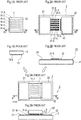
Fig. 1A and Fig. 1B which is a cross-sectional view taken along the line B-B inFig. 1A , anLED element 1 has slender p-side electrodes 11-1, 11-2, ··· , 11-6 electrically connected to a p-type semi conductor region (not shown) and a slender n-side electrode 12 electrically-connected to an n-type semi conductor region (not shown). In this case, each of the electrodes 11-1, 11-2, ··· , 11-6 and 12 viewed from the top has a rectangular shape with a short side and a long side twice or more as long as the short side. Thus, the heat resistance can be decreased and the fluctuation of a forward voltage can be suppressed. Also, since the p-side electrodes 11-1, 11-2, ···, 11-6 are broadly spread on the bottom of theLED element 1, currents from the p-side electrodes 11-1, 11-2, ··· , 11-6 can be spread through an entire active region (not shown) within theLED element 1 to the n-side electrode 12, which can improve the light emitting efficiency and make the light emitting distribution uniform. Note that bonding layers (not shown) including an uppermost Au layer are formed on the p-side electrodes 11-1, 11-2, ···, 11-6 and the n-side electrode12 by a plating process or a sputtering process. - On the other hand, referring to
Fig. 2A and Fig. 2B which is a cross-sectional view taken along the line B-B inFig. 2A , asubmount substrate 2 made of AIN, for example, has a p-sidewiring pattern layer 21 and an n-sidewiring pattern layer 22. The p-sidewiring pattern layer 21 has AuSn layers 31-1, 31-2, ···, 31-6 corresponding to the p-side electrodes 11-1, 11-2, ···, 11-6, respectively, of theLED element 1, and the n-sidewiring pattern layer 22 has anAuSn layer 32 corresponding to the n-side electrode 12 of theLED element 1. Note that bonding layers (not shown) including an uppermost Au layer are formed on the p-sidewiring pattern layer 21 and the n-sidewiring pattern layer 22, and pads (not shown) are formed thereon. - Finally, referring to
Fig. 3A and Fig. 3B which is a cross-sectional view taken along the line B-B inFig. 3A , theLED element 1 ofFigs. 1A and 1B is faced down in a thermal-pressuring process on thesubmount substrate 2 ofFigs. 2A and 2B , so that the uppermost Au layers of the AuSn layer 31-1, 31-2, ···, 31-6 and 32 of thesubmount substrate 2 are eutectic with the uppermost Au layers of the p-side electrodes 11-1, 11-2, ···, 11-6 and the n-side electrode 12 of theLED element 1 to form AuSn eutectic bonding layer 31' -1, 31' -2, ···, 31' -6 and 32'. As a result, the p-side electrodes 11-1, 11-2, ···, 11-6 of theLED element 1 are electrically connected to the p-sidewiring pattern layer 21 of thesubmount substrate 2, and the n-side electrode 12 of theLED element 1 is electrically connected to the n-sidewiring pattern layer 22 of thesubmount substrate 2. Thus, theLED element 1 is bonded by the AuSn eutectic bonding layer 31' -1, 31' -2, ···, 31' -6 and 32' to thesubmount substrate 2, completing a semiconductorlight emitting apparatus 3. - In the semiconductor
light emitting apparatus 3 ofFigs. 3A and 3B , however, the AuSn eutectic bonding layer 31' -1, 31' -2, ···, 31' -6 and 32' has the following bonding defects. - The AuSn layers 31-1, 31-2, ···, 31-6 and 32 of
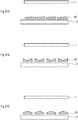
Figs. 2A and 2B are usually formed by a lift-off process. That is, as illustrated inFig. 4A , a photoresist pattern 30-1 for forming the AuSn layers 31-1, 31-2, ···, 31-6 and 32 is formed by a photolithography process on a submount substrate 2 (the p-side wiring pattern layer 21), and then, an AuSn layer 30-2 is deposited on the entire surface by a sputtering process or an evaporating process. Then, as illustrated inFig. 4B , the photoresist pattern layer 30-1 is removed to form the AuSn layers 31-1, 31-2, ··· , 31-6 and 32. In this case, however, when the photoresist pattern layer 30-1 is removed to rupture the AuSn layer 30-2, burrs BR would be created on the edges of the AuSn layers 31-1, 31-2, ···, 31-6 and 32. - Also, the
LED element 1 is bonded on the submount substrate 2 (the p-side wiring pattern layer 21) having the burrs BR as illustrated inFig. 4C , and then, a thermal-pressuring process is carried out, so that only a top part of the burrs BR is dissolved as illustrated inFig. 4D . However, as there is a pressure gradient of the LED element 1 (the p-side electrode 11-6), the amount of the AuSn eutectic bonding layer 31'-1, 31'-2, ···, 31'-6and 32' would be uneven. As a result, the AuSn eutect ic bonding layer 31' -1, 31' -2, ..., 31' -6 and 32' would become uneven to create a large gap G between the LED element 1 (the p-side electrode 11-6) and the submount substrate 2 (the p-side wiring pattern layer 21). That is, only a part of the LED element 1 (the p-side electrode 11-6) can be in contact with the submount substrate 2 (the p-side wiring pattern layer 21), so that the bonding area therebetween would be small. Even when the LED element 1 (the p-side electrode 11-6) is completely in contact with the submount substrate 2 (the p-side wiring pattern layer 21), AuSn would be exposed to a high temperature due to the presence of the burrs BR, and would be thermally oxidized before the burrs BR are dissolved, which would be an obstacle in a eutectic reaction. Thus, a defective bonding would happen between theLED element 1 and thesubmount substrate 2 after the thermal-pressuring process. - Further, since the p-side electrodes 11-1, 11-2, ···, 11-6 and the n-
side electrode 12 and their corresponding AuSn layers 31-1, 31-2, ··· , 31-6 and 32 are s lender, the AuSn layers 31-1, 31-2, ···, 31-6 and 32 would be sloped lengthwise as illustrated inFig. 5A , or the center portions of the AuSn layers 31-1, 31-2, ···, 31-6 and 32 would be deeply concave as illustrated inFig. 5B , or the center portions of the AuSn layers 31-1, 31-2, ···, 31-6 and 32 would be highly convex as illustrated inFig. 5C . In any case, the bonding area between theLED element 1 and thesubmount substrate 2 would be decreased, so that a defective bonding also would happen between theLED element 1 and thesubmount substrate 2 after the thermal-pressuring process. - The above-described defective bonding would invite the fluctuation of the heat resistance and the fluctuation of the forward voltage, which would invite irregular light emitting characteristics.
- Still further, when the burrs BR are created on the edges of the AuSn layers 31-1, 31-2, ···, 31-6 and 32, or the AuSn layers 31-1, 31-2, ··· , 31-6 and 32 are sloped lengthwise, deeply concave or highly convex, the AuSn eutectic bonding layer 31' -1, 31' -2, ···, 31' -6 and 32' after the thermal-pressuring process would protrude from the
LED element 1 as illustrated by X inFigs. 6A and 6B . Particularly, when the AuSn layers 31-1, 31-2, ···, 31-6 and 32 are sloped lengthwise, theLED element 1 would be sloped as illustrated inFig. 6B . As a result, theLED element 1 would be short-circuited to thewiring pattern layer submount substrate 2, so that the semi conductorlight emitting apparatus 3 would not operate. - The presently disclosed subject matter seeks to solve one or more of the above-described problems.
- According to the presently disclosed subject matter, a semiconductor light emitting apparatus includes a semi conductor light emitting element having a first electrode and a second electrode, a substrate having first and second wiring pattern layers electrically-connected to the first and second electrodes, respectively, and multiple conductive bonding layer elements provided between the first electrode and the first wiring pattern layer and/or between the second electrode and the second wiring pattern layer.
- A method for manufacturing a semiconductor light emitting apparatus includes preparing a semiconductor light emitting element having a first electrode and a second electrode, preparing a substrate having first and second wiring pattern layers electrically-connected to the first and second electrodes, respectively, forming multiple conductive bonding layer elements on one of the first electrode and the first wiring pattern layer and/or between the second electrode and the second wiring pattern layer, and carrying out a thermal-pressuring process to bond the first electrode to the first wiring pattern layer and bond the second electrode to the second wiring pattern layer.
- According to the presently disclosed subject matter, a bonding defect between the semiconductor light emitting element and the substrate can be substantially eliminated.
- The above and other advantages and features of the presently disclosed subject matter will be more apparent from the following description of certain embodiments, compared with the prior art, taken in conjunction with the accompanying drawings, wherein:
-
Figs. 1A, 2A and 3A are top views for explaining a prior art method for manufacturing a semiconductor light emitting apparatus; -
Figs. 1B, 2B and 3B are cross-sectional views taken along the line B-B ofFigs. 1A, 2A and 3A , respectively; -
Figs. 4A, 4B, 4C and 4D are cross-sectional views for explaining a problem caused by the prior art method as illustrated inFigs. 1A, 1B, 2A, 2B, 3A and 3B ; -
Figs. 5A, 5B and 5C are cross-sectional views for explaining another problem caused by the prior art method as illustrated inFigs. 1A, 1B, 2A, 2B, 3A and 3B ; -
Fig. 6A is a top view for explaining still another problem caused by the prior art method as illustrated inFigs. 1A, 1B, 2A, 2B, 3A and 3B ; -
Fig. 6B is a cross-sectional view taken along the line B-B ofFig. 6A ; -
Figs. 7A, 8A and 9A are top views for explaining a first embodiment of the method for manufacturing a semiconductor light emitting apparatus according to the presently disclosed subject matter; -
Figs. 7B, 8B and 9B are cross-sectional views taken along the line B-B ofFigs. 7A, 8A and 9A , respectively; -
Figs. 10A, 10B, 10C and 10D are cross-sectional views for explaining an effect caused by the method as illustrated inFigs. 7A, 7B, 8A, 8B, 9A and 9B ; -
Figs. 11A, 11B and 11C are cross-sectional views for explaining another effect caused by the method as illustrated inFigs. 7A, 7B, 8A, 8B, 9A and 9B ; -
Figs. 12A and 12B are a top view and a cross-sectional view illustrating a modification of the submount substrate ofFigs. 8A and 8B ; -
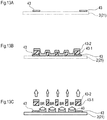
Figs. 13A, 13B and 13C are cross-sectional views for explaining a method for manufacturing the submount substrate ofFigs. 12A and 12B ; -
Figs. 14A, 15A and 16A are top views for explaining a second embodiment of the method for manufacturing a semiconductor light emitting apparatus according to the presently disclosed subject matter; -
Figs. 14B, 15B and 16B are cross-sectional views taken along the line B-B ofFigs. 14A, 15A and 16A , respectively; -
Fig. 17A is a top view for explaining an effect caused by the method as illustrated inFigs. 14A, 14B, 15A, 15B, 16A and 16B ; -
Fig. 17B is a cross-sectional view taken along the line B-B ofFig. 17A ; -
Fig. 18A is a top view for explaining an effect caused by a comparative example; -
Fig. 18B is a cross-sectional view taken along the line B-B ofFig. 18A ; -
Figs. 19A and 19B are a top view and a cross-sectional view illustrating a modification of the submount substrate ofFigs. 15A and 15B ; and -
Figs. 20A and 20B are cross-sectional views for illustrating a modification of the AuSn layers ofFigs. 7A and 8B . - A first embodiment of the method for manufacturing a semi conductor light emitting apparatus will be explained now with reference to
Figs. 7A, 7B, 8A, 8B, 9A and 9B . - First, referring to
Fig. 7A and Fig. 7B which is a cross-sectional view taken along the line B-B inFig. 7A , anLED element 1 the same as illustrated inFigs. 1A and 1B is provided. - On the other hand, referring to
Fig. 8A and Fig. 8B which is a cross-sectional view taken along the line B-B inFig. 8A , asubmount substrate 2 made of AIN, for example, has a p-sidewiring pattern layer 21 and an n-sidewiring pattern layer 22. The p-sidewiring pattern layer 21 has AuSn layers 41-1, 41-2, ···, 41-6 corresponding to the p-side electrodes 11-1, 11-2, ···, 11-6, respectively, of theLED element 1, and the n-sidewiring pattern layer 22 has anAuSn layer 42 corresponding to the n-side electrode 12 of theLED element 1. Each of the AuSn layers 41-1, 41-2, ···, 41-6 and 42 is constructed by a series of about 1 to 5 µm thick discreteAuSn layer elements 40 which are one-dimensionally arranged. For example, each of theAuSn layer elements 40 is square viewed from the top, and has a side whose length is the same as the short side of the electrodes 11-1, 11-2, ···, 11-6 and 12 of theLED element 1. In this case, the spacing between theAuSn layer elements 40 is preferably as small as possible. - Finally, referring to
Fig. 9A and Fig. 9B which is a cross-sectional view taken along the line B-B inFig. 9A , theLED element 1 ofFigs. 7A and 7B is faced down in a thermal-pressuring process on thesubmount substrate 2 ofFigs. 8A and 8B , so that the uppermost Au layers of the AuSn layer 41-1, 41-2, ···, 41-6 and 42 of thesubmount substrate 2 are eutectic with the uppermost Au layers of the p-side electrodes 11-1, 11-2, ···, 11-6 and the n-side electrode 12 of theLED element 1 to form AuSn eutectic bonding layers 41' -1, 41' -2, ··· , 41' -6 and 42' each formed by multiple AuSn eutectic layer elements 40' . As a result, the p-side electrodes 11-1, 11-2, ···, 11-6 of theLED element 1 are electrically connected to the p-sidewiring pattern layer 21 of thesubmount substrate 2, and the n-side electrode 12 of theLED element 1 is electrically connected to the n-sidewiring pattern layer 22 of thesubmount substrate 2. Thus, theLED element 1 is bonded by the AuSn eutectic bonding layers 41' -1, 41' -2, ···, 41' -6 and 42' to thesubmount substrate 2, completing a semiconductorlight emitting apparatus 4. - In the semiconductor
light emitting apparatus 4 ofFigs. 9A and 9B , however, the AuSn eutectic bonding layers 41' -1, 41' -2, ···, 41' -6 and 42' can avoid bonding defects. - The
AuSn layer elements 40 of the AuSn layers 41-1, 41-2, ···, 41-6 and 42 ofFigs. 8A and 8B are formed by a lift-off process. That is, as illustrated inFig. 10A , a photoresist pattern 43-1 for forming the AuSn layers 41-1, 41-2, ···, 41-6 and 42 is formed by a photolithography process on a submount substrate 2 (the p-side wiring pattern layer 21), and then, an about 1 to 5 µm thick AuSn layer 43-2 is deposited on the entire surface by a sputtering process or an evaporating process. Then, as illustrated inFig. 10B , the photoresist pattern layer 43-1 is removed to form theAuSn layer elements 40 of the AuSn layers 41-1, 41-2, ···, 41-6 and 42. Even in this case, when the photoresist pattern layer 43-1 is removed to rupture the AuSn layer 43-2, burrs BR would be created on the edges of theAuSn layer elements 40 of the AuSn layers 41-1, 41-2, ···, 41-6 and 42. - Also, the
LED element 1 is bonded on the submount substrate 2 (the p-side wiring pattern layer 21) having the burrs BR as illustrated inFig. 10C , and then, a thermal-pressuring process is carried out, so that only a top part of the burrs BR is dissolved as illustrated inFig. 10D . Also, as there is a pressure gradient of the LED element 1 (the p-side electrode 11-6), the amount of the AuSn eutectic bonding layer elements 40' would be uneven. As a result, the AuSn eutectic layer elements 40' of the AuSn eutectic bonding layer 41' -1, 41' -2, ···, 41' -6 and 42' would become uneven to create a small gap G' between theLED element 1 and thesubmount substrate 2. That is, only a part of the LED element 1 (the p-side electrode 11-6) can be in contact with thesubmount substrate 2, so that the bonding area therebetween would be small. Even when theLED element 1 is completely in contact with thesubmount substrate 2, AuSn would be exposed to a high temperature due to the presence of the burrs BR, and thermally oxidized before the burrs BR are dissolved, which would be an obstacle in a eutectic reaction. However, since each of the AuSn layer elements 40' ofFig. 10C is much smaller than the AuSn layer 31-1, 31-2, ···, 31-6 and 32 ofFig. 4C , the gap G' ofFig. 10D is much smaller than the gap G ofFig. 4D . Therefore, the unbonded AuSn eutectic bonding layer elements 40' can be decreased to substantially increase the bonding area of the AuSn eutectic bonding layer elements 40' . Thus, a defective bonding would hardly happen between theLED element 1 and thesubmount substrate 2 after the thermal-pressuring process. - Further, although the p-side electrodes 11-1, 11-2, ···, 11-6 and the n-
side electrode 12 are slender, since theAuSn layer elements 40 are short, theAuSn layer elements 40 would be not sloped lengthwise as illustrated inFig. 11A , or the center portions of theAuSn layer elements 40 would be shallowly concave as illustrated inFig. 11B , or the center port ions of theAuSn layer elements 40 would be slightly convex as illustrated inFig. 11C . In any case, the bonding area between theLED element 1 and thesubmount substrate 2 would be increased, so that a defective bonding would hardly happen between theLED element 1 and thesubmount substrate 2 after the thermal-pressuring process. - Thus, the fluctuation of the heat resistance and the fluctuation of the forward voltage can be improved, which would also improve the light emitting characteristics.
- Still further, since the burrs BR created on the edges of the AuSn layers 41-1, 41-2, ···, 41-6 and 42 are small, or the AuSn layers 41-1, 41-2, ···, 41-6 and 42 are not sloped lengthwise, shallowly concave or slightly convex, the AuSn eutectic bonding layers 41' -1, 41' -2, ···, 41' -6 and 42' after the thermal-pressuring process would hardly be protruded from the
LED element 1. In addition, since the burrs BR of the AuSn layers 41-1, 41-2, ···, 41-6 and 42 are small, theLED element 1 would not be sloped. As a result, theLED element 1 would not be short-circuited to the p-sidewiring pattern layer submount substrate 2, so that the semiconductorlight emitting apparatus 4 would operate. -
Fig. 12A is a top view illustrating a modification of thesubmount substrate 2 ofFigs. 8A and 8B , andFig. 12B is a cross-sectional view taken along the line B-B inFig. 12A . - In
Figs. 12A and 12B , AuSn-phobic Cr layers 43 that lack an affinity to repel AuSn are provided adjacent to the ends of the series of theAuSn layer elements 40. Therefore, in a thermal-pressuring process, the AuSn eutectic bonding layers 41' -1, 41' -2, ···, 41' -6 and 42' move away from the Cr layers 43, thus surely preventing the AuSn eutectic bonding layers 41' -1, 41' -2, ··· , 41' -6 and 42' from protruding from theLED element 1 after the thermal-pressuring process. - The Cr layers 43 are formed before the formation of the
AuSn layer elements 40. That is, as illustrated inFig. 13A , an about 0.1 µmthick Cr layer 43 is formed on the p-side wiring pattern layers 21 and 22 of thesubmount substrate 2 by a plating process and a photolithography and etching process. After that, theAuSn layer elements 40 of the AuSn layers 41-1, 41-2, ···, 41-6 and 42 are formed by a lift-off process. That is, as illustrated inFig. 13B , a photoresist pattern 43-1 for forming the AuSn layers 41-1, 41-2, ···, 41-6 and 42 is formed by a photolithography process on a submount substrate 2 (the p-side wiring pattern layer 21), and then, an about 1 to 5 µm thick AuSn layer 43-2 is deposited on the entire surface by a sputtering process or a vacuum depositing process. Then, as illustrated inFig. 13C , the photoresist pattern layer 43-1 is removed to form theAuSn layer elements 40 of the AuSn layers 41-1, 41-2, ···, 41-6 and 42. Even in this case, when the photoresist pattern layer 43-1 is removed to rupture the AuSn layer 43-2, small burrs BR would be created on the edges of theAuSn layer elements 40 of the AuSn layers 41-1, 41-2, ···, 41-6 and 42. - A second embodiment of the method for manufacturing a semi conductor light emitting apparatus will be explained now with reference to
Figs. 14A, 14B, 15A, 15B, 16A and 16B . - First, referring to
Fig. 14A and Fig. 14B which is a cross-sectional view taken along the line B-B inFig. 14A , one broad p-side electrode 11 is provided instead of the p-side electrodes 11-1, 11-2, ···, 11-6 ofFigs. 7A and 7B . - On the other hand, referring to
Fig. 15A and Fig. 15B which is a cross-sectional view taken a long the line B-B inFig. 8A , provided on the p-sidewiring pattern layer 21 is anAuSn layer 41 corresponding to the p-side electrode 11 of theLED element 1. TheAuSn layer 41 is constructed by about 1 to 5 µm thick discreteAuSn layer elements 40 which are two-dimensionally arranged. Also, in this case, each of theAuSn layer elements 40 is square viewed from the top, and the spacing between theAuSn layer elements 40 is preferably as small as possible. - Finally, referring to
Fig. 16A and Fig. 16B which is a cross-sectional view taken along the line B-B inFig. 16A , theLED element 1 ofFigs. 14A and 14B is faced down in a thermal-pressuring process on thesubmount substrate 2 ofFigs. 15A and 15B , so that the uppermost Au layers of theAuSn layer elements 40 of the AuSn layers 41 and 42 of thesubmount substrate 2 are eutectic with the uppermost Au layers of the p-side electrode 11 and the n-side electrode 12 of theLED element 1 to form AuSn eutectic bonding layers 41' and 42' each formed by multiple AuSn eutectic layer elements 40' . As a result, the p-side electrode 11 of theLED element 1 is electrically connected to the p-sidewiring pattern layer 21 of thesubmount substrate 2, and the n-side electrode 12 of theLED element 1 is electrically connected to the n-sidewiring pattern layer 22 of thesubmount substrate 2. Thus, theLED element 1 is bonded by the AuSn eutectic bonding layers 41' and 42' to thesubmount substrate 2, completing a semiconductor light emitting apparatus 4' - Even in the semiconductor light emitting apparatus 4' of
Figs. 16A and 16B , since the bonding defects of the AuSn eutectic bonding layers 41' and 42' can be dissolved, the fluctuation of the heat resistance and the fluctuation of the forward voltage can be improved, which would also improve the light emitting characteristics. - Also, since the burrs BR created on the edges of the AuSn layers 41 and 42 are small, or the AuSn layers 41 and 42 are not sloped lengthwise, shallowly concave or slightly convex, the AuSn eutectic bonding layer 41' -1, 41' -2, ···, 41' -6 and 42' after the thermal-pressuring process would hardly be protruded from the
LED element 1. In addition, since the burrs BR of the AuSn layers 41-1, 41-2, ···, 41-6 and 42 are small, theLED element 1 would not be sloped. As a result, theLED element 1 would not be short-circuited to thewiring pattern layer submount substrate 2, so that the semiconductorlight emitting apparatus 4 would operate. - For example, as illustrated in
Figs. 17A and 17B , each of theAuSn layer elements 40 is shallowly concave. Contrary to this, if theAuSn layer elements 40 are constructed by a singleAuSn layer element 40a as illustrated inFigs. 18A and 18B , the singleAuSn layer element 40a is greatly concave. -
Fig. 19A is a top view illustrating a modification of thesubmount substrate 2 ofFigs. 15A and 15B , andFig. 19B is a cross-sectional view taken along the line B-B inFig. 19A . - In
Figs. 19A and 19B , AuSn-phobic Cr layers 43 that lack an affinity to repel AuSn are provided adjacent to the ends of the rows and columns of theAuSn layer elements 40. Therefore, in a thermal-pressuring process, the AuSn eutectic bonding layers 41' and 42' move away from the Cr layers 43, thus surely preventing the AuSn eutectic bonding layers 41' and 42' from protruding from theLED element 1 after the thermal-pressuring process. - The Cr layers 43 are formed before the formation of the
AuSn layer elements 40 in the same way as inFigs. 13A, 13B and 13C . - In the above-described embodiments, the conductive bonding elements can be provided only between the p-side electrodes 11-1, 11-2, ···, 11-6 of the
LED element 1 and the p-sidewiring pattern layer 21 of thesubmount substrate 2, or the conductive bonding elements can be provided only between the n-side electrode 12 of theLED element 1 and the n-sidewiring pattern layer 22 of thesubmount substrate 2. - Also, in the above-described embodiments, the
AuSn layer elements 40 are provided on the wiring pattern layers 21 and 22 of thesubmount substrate 2; however, as illustrated inFigs. 20A and 20B , theAuSn layer elements 40 can be provided on the p-side electrodes 11-1, 11-2, ···, 11-6 (or 11) and the n-side electrode 12 of theLED element 1. Also, theAuSn layer elements 40 can be formed by a screen printing process other than a lift-off process. - In addition, in the above-described embodiments, the
LED element 1 and thesubmount substrate 2 are bonded by AuSn eutectic bonding layer elements 40' ; however, theLED element 1 and thesubmount substrate 2 are bonded by other conductive bonding elements such as Ag particle sintered elements or Au particle sintered elements. In this case, Ag-phobic layers that lack an affinity to repel Ag or Au-phobic layers that lack an affinity to repel Au can be used instead of the Cr layers 43. - Further, the
LED element 1 can be bonded directly to a conventional substrate without thesubmount substrate 2. - Still further, other semiconductor light emitting elements such as a laser diode (LD) element can be used instead of the
LED element 1. - The semiconductor light emitting apparatus according to the presently disclosed subject matter can be applied to an ultra-violet light emitting apparatus, particularly, to a deep ultra-violet light emitting apparatus.
- It will be apparent to those skilled in the art that various modifications and variations can be made in the presently disclosed subject matter without departing from the spirit or scope of the presently disclosed subject matter. Thus, it is intended that the presently disclosed subject matter covers the modifications and variations of the presently disclosed subject matter provided they come within the scope of the appended claims and their equivalents. All related or prior art references described above and in the Background section of the present specification are hereby incorporated in their entirety by reference.
Claims (12)
- A semiconductor light emitting apparatus comprising:a semiconductor light emitting element (1) having a first electrode (11-1, 11-2, ···, 11-6, 11) and a second electrode (12);a substrate (2) having first and second wiring pattern layers (21, 22) electrically-connected to said first and second electrodes (11-1, 11-2, ···, 11-6, 11; 12), respectively; andmultiple conductive bonding layer elements (40', 41', 42') provided between said first electrode (11-1, 11-2, ···, 11-6, 11) and said first wiring pattern layer (21) and/or between said second electrode (12) and said second wiring pattern layer (22).
- The semiconductor light emitting apparatus as set forth in claim 1, further comprising conductive bonding layer elements-phobic layers (43), that lack an affinity to repel said conductive bonding layer elements (41'-1, 41'-2, ···, 41', 42'), adjacent to ends of said multiple conductive bonding layer elements (41'-1, 41'-2, ···, 41', 42').
- The semiconductor light emitting apparatus as set forth in claim 1, wherein said multiple conductive bonding layer elements (41'-1, 41'-2, ···, 41'-6, 41') are one-dimensionally or two-dimensionally arranged.
- The semiconductor light emitting apparatus as set forth in claim 1, wherein said first electrode is defined as multiple first electrodes (11-1, 11-2, ···, 11-6),
said first and second electrodes (11-1, 11-2, ···, 11-6, 12) being rectangular viewed from the top, and each of said first and second electrodes (11-1, 11-2, ··· , 11-6, 12) having a short side and a long side twice or more as long as said short side. - The semiconductor light emitting apparatus as set forth in claim 1, wherein said conductive bonding layer elements (40', 41', 42') comprise AuSn eutectic bonding layer elements, Ag particle sintered elements or Au particle sintered elements.
- The semiconductor light emitting apparatus as set forth in claim 1, wherein said first electrode comprises a p-side electrode, and where in said second electrode comprises an n-side electrode.
- A method for manufacturing a semiconductor light emitting apparatus comprising:preparing a semiconductor light emitting element (1) having a first electrode (11-1, 11-2, ···, 11-6, 11) and a second electrode (12);preparing a substrate (2) having first and second wiring pattern layers (21, 22) electrically-connected to said first and second electrodes (11-1, 11-2, ···, 11-6, 11; 12), respectively;forming multiple conductive bonding layer elements (40', 41', 42') on one of said first electrode (11-1, 11-2, ···, 11-6, 11) and said first wiring pattern layer (21) and/or between said second electrode (12) and said second wiring pattern layer (22); andcarrying out a thermal pressuring process to bond said first electrode (11-1, 11-2, ···, 11-6, 11) to said first wiring pattern layer (21) and bond said second electrode (12) to said second wiring pattern layer (22).
- The method for manufacturing a semiconductor light emitting apparatus as set forth in claim 7, further comprising forming conductive bond ing layer elements-phobic layers (43), that lack an affinity to repel said multiple conductive bonding layer elements (41'-1, 41'-2, ···, 41', 42'), adjacent to ends of said multiple conductive bonding layer elements (41'-1, 41'-2, ··· , 41', 42').
- The method for manufacturing a semi conductor light emitting apparatus as set forth in claim 7, wherein said multiple conductive bonding layer elements (41'-1, 41'-2, ···, 41'-6, 41') are one-dimensionally or two-dimensionally arranged.
- The method for manufacturing a semi conductor light emitting apparatus as set forth in claim 7, wherein said first electrode is defined as multiple first electrodes (11-1, 11-2, ···, 11-6),
said first and second electrodes (11-1, 11-2, ···, 11-6, 12) being rectangular viewed from the top, and each of said first and second electrodes (11-1, 11-2, ··· , 11-6, 12) having a short side and a long side twice or more as long as said short side. - The method for manufacturing a semi conductor light emitting apparatus as set forth in claim 7, wherein said conductive bonding layer elements (40', 41', 42') comprise AuSn eutectic bonding layer elements, Ag particle sintered elements or Au particle sintered elements.
- The method for manufacturing a semi conductor light emitting apparatus as set forth in claim 7, wherein said first electrode comprises a p-side electrode, and wherein said second electrode comprises an n-side electrode.
Applications Claiming Priority (1)
| Application Number | Priority Date | Filing Date | Title |
|---|---|---|---|
| JP2018099340A JP7218048B2 (en) | 2018-05-24 | 2018-05-24 | Semiconductor light emitting device and manufacturing method thereof |
Publications (1)
| Publication Number | Publication Date |
|---|---|
| EP3573114A1 true EP3573114A1 (en) | 2019-11-27 |
Family
ID=66625791
Family Applications (1)
| Application Number | Title | Priority Date | Filing Date |
|---|---|---|---|
| EP19175494.4A Pending EP3573114A1 (en) | 2018-05-24 | 2019-05-20 | Semiconductor light emitting apparatus having multiple conductive bonding layer elements and its manufacturing method |
Country Status (4)
| Country | Link |
|---|---|
| US (1) | US20190363233A1 (en) |
| EP (1) | EP3573114A1 (en) |
| JP (1) | JP7218048B2 (en) |
| CN (1) | CN110534636B (en) |
Families Citing this family (1)
| Publication number | Priority date | Publication date | Assignee | Title |
|---|---|---|---|---|
| JP6803595B1 (en) * | 2020-09-16 | 2020-12-23 | アルディーテック株式会社 | Semiconductor light emitting device chip integration device and its manufacturing method |
Citations (9)
| Publication number | Priority date | Publication date | Assignee | Title |
|---|---|---|---|---|
| US20020190260A1 (en) * | 1999-12-22 | 2002-12-19 | Yu-Chen Shen | Selective placement of quantum wells in flipchip light emitting diodes for improved light extraction |
| EP1531492A2 (en) * | 2003-11-14 | 2005-05-18 | Stanley Electric Co., Ltd. | Semiconductor device and its manufacturing method capable of preventing short circuit of electrodes when semiconductor device is mounted on sub-mount substrate |
| US20100117114A1 (en) * | 2008-11-13 | 2010-05-13 | Ryo Suzuki | Semiconductor light-emitting apparatus and method of fabricating the same |
| EP2207210A1 (en) * | 2007-11-01 | 2010-07-14 | Panasonic Corporation | Semiconductor light emitting element and semiconductor light emitting device using the same |
| EP2219232A1 (en) * | 2007-11-15 | 2010-08-18 | Panasonic Corporation | Semiconductor light emitting device |
| US20100219444A1 (en) * | 2009-02-27 | 2010-09-02 | Toyoda Gosei Co., Ltd. | Manufacturing method of mounting part of semiconductor light emitting element, manufacturing method of light emitting device, and semiconductor light emitting element |
| US20100227421A1 (en) * | 2009-03-04 | 2010-09-09 | Koninklijke Philips Electronics N.V. | Method of bonding a semiconductor device using a compliant bonding structure |
| US20150287900A1 (en) * | 2010-11-05 | 2015-10-08 | Seoul Viosys Co., Ltd. | Light emitting diode assembly and method for fabricating the same |
| JP2018099340A (en) | 2016-12-20 | 2018-06-28 | 株式会社大一商会 | Game machine |
Family Cites Families (11)
| Publication number | Priority date | Publication date | Assignee | Title |
|---|---|---|---|---|
| JP4617902B2 (en) * | 2005-01-31 | 2011-01-26 | 信越半導体株式会社 | Light emitting device and method for manufacturing light emitting device |
| JP5272287B2 (en) * | 2006-03-17 | 2013-08-28 | 日亜化学工業株式会社 | Light emitting device |
| TWI318013B (en) * | 2006-09-05 | 2009-12-01 | Epistar Corp | A light emitting device and the manufacture method thereof |
| JP2008072039A (en) * | 2006-09-15 | 2008-03-27 | Matsushita Electric Ind Co Ltd | Light emitting element |
| JP4846515B2 (en) * | 2006-10-18 | 2011-12-28 | 株式会社東芝 | Optical semiconductor device and method for manufacturing optical semiconductor device |
| CN101359704B (en) * | 2007-07-30 | 2010-06-09 | 晶元光电股份有限公司 | Light emitting element and method for manufacturing the same |
| JP5518273B1 (en) * | 2012-09-14 | 2014-06-11 | パナソニック株式会社 | Light emitting diode element and light emitting diode device |
| KR20140094752A (en) * | 2013-01-22 | 2014-07-31 | 삼성전자주식회사 | An electronic device package and a packaging substrate for the same |
| JP6023660B2 (en) * | 2013-05-30 | 2016-11-09 | スタンレー電気株式会社 | Semiconductor light emitting device and semiconductor light emitting device |
| JP6760921B2 (en) * | 2014-07-31 | 2020-09-23 | ソウル バイオシス カンパニー リミテッドSeoul Viosys Co.,Ltd. | Light emitting diode |
| JP6780293B2 (en) * | 2016-05-24 | 2020-11-04 | 日亜化学工業株式会社 | Manufacturing method of light emitting device |
-
2018
- 2018-05-24 JP JP2018099340A patent/JP7218048B2/en active Active
-
2019
- 2019-05-13 US US16/410,881 patent/US20190363233A1/en not_active Abandoned
- 2019-05-20 EP EP19175494.4A patent/EP3573114A1/en active Pending
- 2019-05-22 CN CN201910428116.8A patent/CN110534636B/en active Active
Patent Citations (9)
| Publication number | Priority date | Publication date | Assignee | Title |
|---|---|---|---|---|
| US20020190260A1 (en) * | 1999-12-22 | 2002-12-19 | Yu-Chen Shen | Selective placement of quantum wells in flipchip light emitting diodes for improved light extraction |
| EP1531492A2 (en) * | 2003-11-14 | 2005-05-18 | Stanley Electric Co., Ltd. | Semiconductor device and its manufacturing method capable of preventing short circuit of electrodes when semiconductor device is mounted on sub-mount substrate |
| EP2207210A1 (en) * | 2007-11-01 | 2010-07-14 | Panasonic Corporation | Semiconductor light emitting element and semiconductor light emitting device using the same |
| EP2219232A1 (en) * | 2007-11-15 | 2010-08-18 | Panasonic Corporation | Semiconductor light emitting device |
| US20100117114A1 (en) * | 2008-11-13 | 2010-05-13 | Ryo Suzuki | Semiconductor light-emitting apparatus and method of fabricating the same |
| US20100219444A1 (en) * | 2009-02-27 | 2010-09-02 | Toyoda Gosei Co., Ltd. | Manufacturing method of mounting part of semiconductor light emitting element, manufacturing method of light emitting device, and semiconductor light emitting element |
| US20100227421A1 (en) * | 2009-03-04 | 2010-09-09 | Koninklijke Philips Electronics N.V. | Method of bonding a semiconductor device using a compliant bonding structure |
| US20150287900A1 (en) * | 2010-11-05 | 2015-10-08 | Seoul Viosys Co., Ltd. | Light emitting diode assembly and method for fabricating the same |
| JP2018099340A (en) | 2016-12-20 | 2018-06-28 | 株式会社大一商会 | Game machine |
Also Published As
| Publication number | Publication date |
|---|---|
| CN110534636B (en) | 2024-07-02 |
| US20190363233A1 (en) | 2019-11-28 |
| CN110534636A (en) | 2019-12-03 |
| JP7218048B2 (en) | 2023-02-06 |
| JP2019204885A (en) | 2019-11-28 |
Similar Documents
| Publication | Publication Date | Title |
|---|---|---|
| KR101546929B1 (en) | Light emitting diode and led module having the same | |
| US8193015B2 (en) | Method of forming a light-emitting-diode array with polymer between light emitting devices | |
| CN112602200A (en) | Light emitting element | |
| JP5602207B2 (en) | Display device | |
| US10381400B2 (en) | Method of manufacturing light emitting device | |
| WO2017159129A1 (en) | Glass wiring substrate and method for producing same, component mounted glass wiring substrate and method for producing same, and substrate for display devices | |
| US10658423B2 (en) | Method of manufacturing light emitting device | |
| JP2010251693A (en) | Light emitting diode device and manufacturing method thereof | |
| TW201735348A (en) | Light-emitting element assembly, method of manufacturing the same, and display device | |
| CN107567671B (en) | Monolithic diode laser arrangement | |
| NL1029688C2 (en) | Method for manufacturing an electrical circuit provided with a plurality of LEDs. | |
| CN113675305B (en) | Light emitting diode chips and display devices | |
| US7442565B2 (en) | Method for manufacturing vertical structure light emitting diode | |
| KR20050018592A (en) | Light-emitting diode array | |
| CN114762201B (en) | Semiconductor laser element and method for manufacturing the same, and semiconductor laser device | |
| DE102010009455A1 (en) | Semiconductor laser device has semiconductor laser chip incorporating active layer, that is arranged on submount | |
| CN110534636B (en) | Semiconductor light emitting device having multiple conductive bonding layer elements and method of manufacturing the same | |
| JP2015032869A (en) | Line light source device | |
| JP4058937B2 (en) | Semiconductor light emitting device and manufacturing method thereof | |
| JP2015126077A (en) | Light-emitting component, light-emitting device, and manufacturing method thereof | |
| JPH10335696A (en) | Light emitting diode array | |
| JP2025072644A (en) | Light emitting module and manufacturing method thereof | |
| TW202347814A (en) | Semiconductor light-emitting device | |
| KR102149911B1 (en) | Light emitting diode and led module having the same | |
| CN118541886A (en) | Optical semiconductor device |
Legal Events
| Date | Code | Title | Description |
|---|---|---|---|
| PUAI | Public reference made under article 153(3) epc to a published international application that has entered the european phase |
Free format text: ORIGINAL CODE: 0009012 |
|
| STAA | Information on the status of an ep patent application or granted ep patent |
Free format text: STATUS: THE APPLICATION HAS BEEN PUBLISHED |
|
| AK | Designated contracting states |
Kind code of ref document: A1 Designated state(s): AL AT BE BG CH CY CZ DE DK EE ES FI FR GB GR HR HU IE IS IT LI LT LU LV MC MK MT NL NO PL PT RO RS SE SI SK SM TR |
|
| AX | Request for extension of the european patent |
Extension state: BA ME |
|
| STAA | Information on the status of an ep patent application or granted ep patent |
Free format text: STATUS: REQUEST FOR EXAMINATION WAS MADE |
|
| 17P | Request for examination filed |
Effective date: 20200330 |
|
| RBV | Designated contracting states (corrected) |
Designated state(s): AL AT BE BG CH CY CZ DE DK EE ES FI FR GB GR HR HU IE IS IT LI LT LU LV MC MK MT NL NO PL PT RO RS SE SI SK SM TR |
|
| STAA | Information on the status of an ep patent application or granted ep patent |
Free format text: STATUS: EXAMINATION IS IN PROGRESS |
|
| 17Q | First examination report despatched |
Effective date: 20211007 |
|
| REG | Reference to a national code |
Ref country code: DE Ref legal event code: R079 Free format text: PREVIOUS MAIN CLASS: H01L0033620000 Ipc: H10H0020857000 |
|
| GRAP | Despatch of communication of intention to grant a patent |
Free format text: ORIGINAL CODE: EPIDOSNIGR1 |
|
| RIC1 | Information provided on ipc code assigned before grant |
Ipc: H10H 20/857 20250101AFI20260421BHEP Ipc: H10H 20/01 20250101ALI20260421BHEP Ipc: H10H 20/831 20250101ALN20260421BHEP Ipc: H10H 20/858 20250101ALN20260421BHEP |
|
| STAA | Information on the status of an ep patent application or granted ep patent |
Free format text: STATUS: GRANT OF PATENT IS INTENDED |
|
| INTG | Intention to grant announced |
Effective date: 20260528 |