EP3572725A1 - Light emitting element, fluorescent light source device - Google Patents
Light emitting element, fluorescent light source device Download PDFInfo
- Publication number
- EP3572725A1 EP3572725A1 EP18741463.6A EP18741463A EP3572725A1 EP 3572725 A1 EP3572725 A1 EP 3572725A1 EP 18741463 A EP18741463 A EP 18741463A EP 3572725 A1 EP3572725 A1 EP 3572725A1
- Authority
- EP
- European Patent Office
- Prior art keywords
- layer
- excitation light
- light source
- fluorescent
- emitting element
- Prior art date
- Legal status (The legal status is an assumption and is not a legal conclusion. Google has not performed a legal analysis and makes no representation as to the accuracy of the status listed.)
- Granted
Links
Images



Classifications
-
- F—MECHANICAL ENGINEERING; LIGHTING; HEATING; WEAPONS; BLASTING
- F21—LIGHTING
- F21V—FUNCTIONAL FEATURES OR DETAILS OF LIGHTING DEVICES OR SYSTEMS THEREOF; STRUCTURAL COMBINATIONS OF LIGHTING DEVICES WITH OTHER ARTICLES, NOT OTHERWISE PROVIDED FOR
- F21V7/00—Reflectors for light sources
- F21V7/22—Reflectors for light sources characterised by materials, surface treatments or coatings, e.g. dichroic reflectors
- F21V7/28—Reflectors for light sources characterised by materials, surface treatments or coatings, e.g. dichroic reflectors characterised by coatings
- F21V7/30—Reflectors for light sources characterised by materials, surface treatments or coatings, e.g. dichroic reflectors characterised by coatings the coatings comprising photoluminescent substances
-
- F—MECHANICAL ENGINEERING; LIGHTING; HEATING; WEAPONS; BLASTING
- F21—LIGHTING
- F21V—FUNCTIONAL FEATURES OR DETAILS OF LIGHTING DEVICES OR SYSTEMS THEREOF; STRUCTURAL COMBINATIONS OF LIGHTING DEVICES WITH OTHER ARTICLES, NOT OTHERWISE PROVIDED FOR
- F21V9/00—Elements for modifying spectral properties, polarisation or intensity of the light emitted, e.g. filters
- F21V9/30—Elements containing photoluminescent material distinct from or spaced from the light source
-
- C—CHEMISTRY; METALLURGY
- C09—DYES; PAINTS; POLISHES; NATURAL RESINS; ADHESIVES; COMPOSITIONS NOT OTHERWISE PROVIDED FOR; APPLICATIONS OF MATERIALS NOT OTHERWISE PROVIDED FOR
- C09K—MATERIALS FOR MISCELLANEOUS APPLICATIONS, NOT PROVIDED FOR ELSEWHERE
- C09K11/00—Luminescent materials, e.g. electroluminescent or chemiluminescent
- C09K11/08—Luminescent materials, e.g. electroluminescent or chemiluminescent containing inorganic luminescent materials
- C09K11/77—Luminescent materials, e.g. electroluminescent or chemiluminescent containing inorganic luminescent materials containing rare earth metals
- C09K11/7766—Luminescent materials, e.g. electroluminescent or chemiluminescent containing inorganic luminescent materials containing rare earth metals containing two or more rare earth metals
- C09K11/7774—Aluminates
-
- F—MECHANICAL ENGINEERING; LIGHTING; HEATING; WEAPONS; BLASTING
- F21—LIGHTING
- F21S—NON-PORTABLE LIGHTING DEVICES; SYSTEMS THEREOF; VEHICLE LIGHTING DEVICES SPECIALLY ADAPTED FOR VEHICLE EXTERIORS
- F21S2/00—Systems of lighting devices, not provided for in main groups F21S4/00 - F21S10/00 or F21S19/00, e.g. of modular construction
-
- F—MECHANICAL ENGINEERING; LIGHTING; HEATING; WEAPONS; BLASTING
- F21—LIGHTING
- F21V—FUNCTIONAL FEATURES OR DETAILS OF LIGHTING DEVICES OR SYSTEMS THEREOF; STRUCTURAL COMBINATIONS OF LIGHTING DEVICES WITH OTHER ARTICLES, NOT OTHERWISE PROVIDED FOR
- F21V7/00—Reflectors for light sources
- F21V7/10—Construction
-
- F—MECHANICAL ENGINEERING; LIGHTING; HEATING; WEAPONS; BLASTING
- F21—LIGHTING
- F21V—FUNCTIONAL FEATURES OR DETAILS OF LIGHTING DEVICES OR SYSTEMS THEREOF; STRUCTURAL COMBINATIONS OF LIGHTING DEVICES WITH OTHER ARTICLES, NOT OTHERWISE PROVIDED FOR
- F21V7/00—Reflectors for light sources
- F21V7/22—Reflectors for light sources characterised by materials, surface treatments or coatings, e.g. dichroic reflectors
-
- F—MECHANICAL ENGINEERING; LIGHTING; HEATING; WEAPONS; BLASTING
- F21—LIGHTING
- F21V—FUNCTIONAL FEATURES OR DETAILS OF LIGHTING DEVICES OR SYSTEMS THEREOF; STRUCTURAL COMBINATIONS OF LIGHTING DEVICES WITH OTHER ARTICLES, NOT OTHERWISE PROVIDED FOR
- F21V7/00—Reflectors for light sources
- F21V7/22—Reflectors for light sources characterised by materials, surface treatments or coatings, e.g. dichroic reflectors
- F21V7/24—Reflectors for light sources characterised by materials, surface treatments or coatings, e.g. dichroic reflectors characterised by the material
-
- F—MECHANICAL ENGINEERING; LIGHTING; HEATING; WEAPONS; BLASTING
- F21—LIGHTING
- F21V—FUNCTIONAL FEATURES OR DETAILS OF LIGHTING DEVICES OR SYSTEMS THEREOF; STRUCTURAL COMBINATIONS OF LIGHTING DEVICES WITH OTHER ARTICLES, NOT OTHERWISE PROVIDED FOR
- F21V7/00—Reflectors for light sources
- F21V7/22—Reflectors for light sources characterised by materials, surface treatments or coatings, e.g. dichroic reflectors
- F21V7/24—Reflectors for light sources characterised by materials, surface treatments or coatings, e.g. dichroic reflectors characterised by the material
- F21V7/26—Reflectors for light sources characterised by materials, surface treatments or coatings, e.g. dichroic reflectors characterised by the material the material comprising photoluminescent substances
-
- F—MECHANICAL ENGINEERING; LIGHTING; HEATING; WEAPONS; BLASTING
- F21—LIGHTING
- F21V—FUNCTIONAL FEATURES OR DETAILS OF LIGHTING DEVICES OR SYSTEMS THEREOF; STRUCTURAL COMBINATIONS OF LIGHTING DEVICES WITH OTHER ARTICLES, NOT OTHERWISE PROVIDED FOR
- F21V7/00—Reflectors for light sources
- F21V7/22—Reflectors for light sources characterised by materials, surface treatments or coatings, e.g. dichroic reflectors
- F21V7/28—Reflectors for light sources characterised by materials, surface treatments or coatings, e.g. dichroic reflectors characterised by coatings
-
- G—PHYSICS
- G02—OPTICS
- G02B—OPTICAL ELEMENTS, SYSTEMS OR APPARATUS
- G02B5/00—Optical elements other than lenses
- G02B5/08—Mirrors
-
- G—PHYSICS
- G02—OPTICS
- G02B—OPTICAL ELEMENTS, SYSTEMS OR APPARATUS
- G02B5/00—Optical elements other than lenses
- G02B5/08—Mirrors
- G02B5/0816—Multilayer mirrors, i.e. having two or more reflecting layers
- G02B5/085—Multilayer mirrors, i.e. having two or more reflecting layers at least one of the reflecting layers comprising metal
- G02B5/0875—Multilayer mirrors, i.e. having two or more reflecting layers at least one of the reflecting layers comprising metal the reflecting layers comprising two or more metallic layers
-
- G—PHYSICS
- G02—OPTICS
- G02B—OPTICAL ELEMENTS, SYSTEMS OR APPARATUS
- G02B5/00—Optical elements other than lenses
- G02B5/20—Filters
-
- F—MECHANICAL ENGINEERING; LIGHTING; HEATING; WEAPONS; BLASTING
- F21—LIGHTING
- F21Y—INDEXING SCHEME ASSOCIATED WITH SUBCLASSES F21K, F21L, F21S and F21V, RELATING TO THE FORM OR THE KIND OF THE LIGHT SOURCES OR OF THE COLOUR OF THE LIGHT EMITTED
- F21Y2115/00—Light-generating elements of semiconductor light sources
- F21Y2115/20—Electroluminescent [EL] light sources
-
- F—MECHANICAL ENGINEERING; LIGHTING; HEATING; WEAPONS; BLASTING
- F21—LIGHTING
- F21Y—INDEXING SCHEME ASSOCIATED WITH SUBCLASSES F21K, F21L, F21S and F21V, RELATING TO THE FORM OR THE KIND OF THE LIGHT SOURCES OR OF THE COLOUR OF THE LIGHT EMITTED
- F21Y2115/00—Light-generating elements of semiconductor light sources
- F21Y2115/30—Semiconductor lasers
Definitions
- the present invention relates to a light emitting element including a fluorescent body. Also, the present invention relates to a fluorescent light source device including the light emitting element and an excitation light source, the fluorescent light source device exciting a fluorescent body with excitation light emitted from the excitation light source to radiate fluorescence.
- Patent Document 1 discloses a fluorescent light source device in which the surface on which the laser beam enters the fluorescent body and the surface from which fluorescence is extracted from the fluorescent body are configured by the same surface.
- Patent Document 1 JP-A-2015-50124
- FIG. 9 is a view schematically showing a fluorescent light source device disclosed in Patent Document 1.
- a fluorescent light source device 100 includes an excitation light source 110 and a light emitting element 120.
- the light emitting element 120 includes a substrate 121, and a bonding layer 122, a reflection layer 123, an enhanced reflection layer 124, a total reflection layer 125, and a fluorescent body layer 126 formed on the substrate 121.
- the fluorescent body layer 126 includes a predetermined fluorescent body, and when excitation light 131 having a predetermined wavelength emitted from the excitation light source 110 is entered, the fluorescent body is excited to generate fluorescence 132 having a longer wavelength than the excitation light.
- the fluorescence 132 is radiated outside from the surface of the side far from the substrate 121 of the surfaces of the fluorescent body layer 126, namely the surface on which the excitation light 131 is entered.
- this surface is called "light extraction surface”.
- the fluorescence 132 generated in the fluorescent body layer 126 does not necessarily advance only on the light extraction surface, but advances in the opposite direction, namely, in the direction toward the substrate 121.
- the fluorescent light source device 100 is also provided with layers for reflection (123, 124, 125) so as to effectively extract this fluorescence 132 as well.
- the reflection layer 123 is provided so as to direct the fluorescence 132 having passed through the total reflection layer 125 and the enhanced reflection layer 124 and advanced on the side of the substrate 121 toward the side of the light extraction surface, and is configured by a layer having especially high reflectance.
- the reflection layer 123 can be formed of Ag or Al, and is generally formed of Ag, in particular.
- the present inventors For the purpose of increasing the intensity of the fluorescence emitted from the fluorescent light source device 100, the present inventors made the excitation light 131 enter the light emitting element 120 at an intensity higher than the intensity that is conventionally considered to be general. Then, the present inventors newly found that the illuminance maintenance factor of the light emitting element 120 rapidly decreases in comparison with the case where the excitation light 131 enters at a conventional intensity.
- the light emitting element according to the present invention includes:
- the present inventors made the excitation light 131 having high intensity enter for a long time, and analyzed the conventional light emitting element 120 in the condition that the illuminance maintenance factor is decreased. It was found that a material layer that is different from that in an early stage invaded inside the enhanced reflection layer 124. This layer was analyzed, and it was found that the layer was formed of a material containing Ag. It was also found that the material containing Ag did not invade the bonding layer 122 side.
- the present inventors made the excitation light 131 having a conventional degree of intensity enter the conventional light emitting element 120 for an equivalent time. At this time, the illuminance maintenance factor of the light emitting element 120 little decreased, and invasion of the material containing Ag into the enhanced reflection layer 124 was not observed in analysis of the element.
- the present inventors inferred that incidence of the excitation light 131 having a very high intensity and the fluorescence 132 generated in the fluorescent body layer 126 into the reflection layer 123 resulted in diffusion of the Ag component contained in the reflection layer 123 only on the side of the light extraction surface for some reason, and invasion into the enhanced reflection layer 124. It is considered that the Ag component actually invaded as Ag + , and precipitated as an Ag compound in the enhanced reflection layer 124. Presence of an Ag compound in the enhanced reflection layer 124 causes decrease in reflectance and transmittance in that region. Further, formation of an Ag compound containing a constituting element of the enhanced reflection layer 124 in a region neighboring the enhanced reflection layer 124 in the reflection layer 123 results in decrease in reflectance of the region. It is inferred that these phenomena caused decrease in illuminance maintenance factor.
- the Ag component should diffuse also in the direction of the substrate 121.
- the material containing Ag does not invade on the bonding layer 122 side. From this result, the inventors inferred that the Ag component diffused on the light extraction surface side by a mechanism that is different from migration by heat as is conventionally known. Although this mechanism is not certain at present, the present inventors consider as follows.
- the intense excitation light 131 irradiating the fluorescent body layer 126, and the fluorescence 132 generated in the fluorescent body layer 126 by excitation by the excitation light 131 partly advance in the direction of the substrate 121.
- the light having passed through the enhanced reflection layer 124 enters a surface of the reflection layer 123.
- the layers of the enhanced reflection layer 124 when the layer located closest to the reflection layer 123 (hereinafter, referred to as "specific layer") is amorphous, electron-hole pairs are generated in the layer by the intense excitation light 131 and the fluorescence 132.
- a diffusion prevention layer configured by a layer that is at least partly crystallized is formed between the reflection layer and the enhanced reflection layer.
- the diffusion prevention layer is configured to have high density, and contains less dangling bonds compared with the amorphous layer. This prevents diffusion of atoms of metal atoms constituting the reflection layer on the light extraction surface side from the diffusion prevention layer. Accordingly, even when intense excitation light enters the light emitting element, it is possible to maintain the high illuminance for a long time. The same effect is realized not only in the case where the reflection layer is formed of Ag or metal containing Ag, but also in the case where the reflection layer is formed of Al or metal containing Al.
- a total reflection layer may be provided between the enhanced reflection layer and the fluorescent body layer.
- the diffusion prevention layer be configured to have high density.
- the diffusion prevention layer has a density of preferably more than 3.82 g/cm 3 , more preferably 3.92 g/cm 3 or more. This point will be described later in "MODE FOR CARRYING OUT THE INVENTION".
- the diffusion prevention layer can be configured by an oxide layer, a nitride layer, or a fluoride layer.
- the oxide layer include Al 2 O 3 , SiO 2 , TiO 2 , Ta 2 O 5 , ZrO 2 , and Nb 2 O 5 .
- the nitride layer include SiN.
- the fluoride layer include MgF 2 and CaF 2 .
- the fluorescent light source device includes:
- a fluorescent light source device capable of maintaining high fluorescent intensity for a long time is realized.
- a light emitting element and a fluorescent light source device capable of maintaining high fluorescent intensity for a long time is realized.
- Fig. 1 is a view schematically showing a configuration of one embodiment of a fluorescent light source device.
- a fluorescent light source device 1 shown in Fig. 1 includes an excitation light source 2, a dichroic mirror 3, and a light emitting element 10.
- the excitation light source 2 includes a semiconductor laser device that emits light in the blue region having a wavelength of 445 nm or more and 465 nm or less, for example.
- the excitation light source 2 may include an optical system such as a collimator lens as necessary.
- the light emitting element 10 includes a fluorescent body as will be described later.
- the fluorescent body included in the light emitting element 10 is excited, and fluorescence 22 is radiated from the light emitting element 10.
- the fluorescence 22 is light having a longer wavelength than the excitation light 21, and has a wavelength of 470 nm or more and 700 nm or less, for example.
- the dichroic mirror 3 is configured to transmit the excitation light 21 emitted from the excitation light source 2, while reflecting the fluorescence 22 emitted from the light emitting element 10.
- the dichroic mirror 3 is arranged so that the mirror surface is inclined at an angle of 45° to the incidence angle of the excitation light 21, for example. With such a configuration, the fluorescence 22 is extracted outside the fluorescent light source device 1, and enters a subsequent optical system (not shown), for example.
- the optical arranging method of the fluorescent light source device 1 including the dichroic mirror 3 as shown in Fig. 1 is merely one example, and any arrangement form is possible.
- Fig. 2 is a sectional view schematically showing a configuration of the light emitting element 10.
- the light emitting element 10 has a substrate 11, a bonding layer 12, a reflection layer 13, a diffusion prevention layer 14, an enhanced reflection layer 15, and a fluorescent body layer 16.
- the substrate 11 is provided for supporting the fluorescent body layer 16 and discharging the heat emitted in the fluorescent body layer 16.
- the substrate 11 is formed of a material having a thermal conductivity of 90 W/(m- K) or more, specifically, 230 to 400 W/(m- K), for example. Examples of such a material include Cu, copper compounds (MoCu, CuW and the like), and Al.
- the thickness of the substrate 11 is, for example, 0.5 to 5 mm. From the viewpoint of heat discharge property or the like, it is preferred that the area in the surface of the substrate 11 be larger than the area of the fluorescent body layer 16.
- the bonding layer 12 is a layer for bonding the substrate 11, and other layer including the fluorescent body layer 16, and is formed, for example, of a solder material. From the viewpoint of heat discharge property or the like, it is preferred to use, for example, a material having a thermal conductivity of 40 W/(m ⁇ K) or more as a material forming the bonding layer 12. More specifically, for example, a cream solder prepared by mixing flux and other impurities with a material such as Sn, Pb and the like to give a creamy (pasty) state, an Sn-Ag-Cu solder, an Au-Sn solder and the like can be used.
- the thickness of the bonding layer 12 is, for example, 20 to 200 ⁇ m.
- a metal film of a Ni/Au film formed, for example, by plating may be formed between the substrate 11 and the bonding layer 12.
- the reflection layer 13 is formed on the upper layer of the bonding layer 12.
- the reflection layer 13 is provided for reflecting fluorescence that has advanced on the surface opposite to the light extraction surface (on the substrate 11 side) of the fluorescent body layer 16 of the fluorescence 22 generated in the fluorescent body layer 16, and guiding the fluorescence to the light extraction surface side.
- the reflection layer 13 is formed of a material having high reflectance (for example, 70% or more) for the fluorescence 22 generated in the fluorescent body layer 16, and is formed, for example, of metal consisting of Al or Ag, or a material film containing the metal.
- the reflection layer 13 is formed of Ag.
- the thickness of the reflection layer 13 is, for example, 100 nm or more and 200 nm or less, and more preferably 120 nm or more and 180 nm or less.
- a metal film of a Ni/Pt/Au film or a Ni/Au film, formed, for example, by vapor deposition may be formed on a surface of the reflection layer 13 on the substrate 11 side.
- the diffusion prevention layer 14 is located between the reflection layer 13 and the enhanced reflection layer 15, and is formed in contact with a surface of the reflection layer 13 on the side opposite to the substrate 11.
- the diffusion prevention layer 14 is formed of a layer that is at least partly crystallized, and is not amorphous.
- the diffusion prevention layer 14 may be formed of a layer that is completely crystalized in the overall region.
- a reflection high energy electron diffraction (RHEED) can be recited.
- a reflection high energy electron diffraction image of the diffusion prevention layer 14 that is partly crystalized shows a ring-like or a dotted pattern according to the crystal orientation.
- a reflection high energy electron diffraction image of an amorphous layer shows a halo-like (blurred ring-like) pattern. Therefore, the condition of the crystallization can be recognized according to the difference in shape of the reflection high energy electron diffraction image of the objective layer.
- the diffusion prevention layer 14 is formed of TiO 2 that is at least partly crystalized. At least partial crystallization realizes the high density of the diffusion prevention layer 14. Specifically, the density of the diffusion prevention layer 14 is higher than 3.82 g/cm 3 , preferably 3.92 g/cm 3 or more. The density of the diffusion prevention layer 14 can be determined from the relation between the refractive index and the density.
- the diffusion prevention layer 14 is not limited to TiO 2 , but may be formed of an oxide layer formed of Al 2 O 3 , SiO 2 , Ta 2 O 5 , ZrO 2 , or Nb 2 O 5 and the like, a nitride layer formed of SiN or the like, or a fluoride layer formed of MgF 2 , CaF 2 or the like.
- the diffusion prevention layer 14 be formed of an oxide layer.
- the diffusion prevention layer 14 be formed of TiO 2 .
- Formation of the diffusion prevention layer 14 that is at least partly crystallized can be realized by an EB-IAD method in which vapor deposition is conducted under irradiation with argon ion, for example.
- vapor deposition using the EB method is generally used, and in this case, the deposited TiO 2 is amorphous.
- the thickness of the diffusion prevention layer 14 is for example, 5 nm or more and 200 nm or less, more preferably 50 nm or more and 100 nm or less.
- the enhanced reflection layer 15 is formed in contact with a surface of the diffusion prevention layer 14 on the side opposite to the substrate 11.
- the enhanced reflection layer 15 is an optical multilayer film in which a low refractive index material layer (Low) and a high refractive index material layer (High) are alternately laminated.
- the thickness of each layer constituting the enhanced reflection layer 15 is about 1/4 of the wavelength of the fluorescence 22, and is, for example, 5 nm or more and 200 nm or less, more preferably 50 nm or more and 100 nm or less.
- the overall thickness of the enhanced reflection layer 15 is 10 nm or more and 500 nm or less, more preferably 50 nm or more and 200 nm or less.
- the layer constituting the enhanced reflection layer 15 may be amorphous, or at least partly crystalized. It suffices that the enhanced reflection layer 15 is provided with at least one low refractive index material layer and at least one high refractive index material layer, and the lamination may be repeated two or more times. When the low refractive index material layer and the high refractive index material layer are laminated repeatedly, the film thickness of each low refractive index material layer and the film thickness of each high refractive index material layer are not necessarily identical.
- the fluorescent body layer 16 is formed on the upper layer of the enhanced reflection layer 15. Upon incidence of the excitation light 21 emitted from the excitation light source 2, the fluorescent body layer 16 generates and radiates fluorescence 22.
- the fluorescent body layer 16 assumes a rectangular plate-like structure, as one example.
- the thickness of the fluorescent body layer 16 is, for example, 0.05 to 1 mm.
- the fluorescent body layer 16 includes a fluorescent body. More specifically, the fluorescent body layer 16 is formed of a monocrystalline or polycrystalline fluorescent body, or a sintered body of a mixture of the fluorescent body and a ceramic binder. That is, the fluorescent body layer 16 is formed of a monocrystalline or polycrystalline fluorescent body.
- the sintered body of a mixture of a fluorescent body and a ceramic binder used in the fluorescent body layer 16 for example, alumina particles of nano size are used as the ceramic binder. Then the sintered body can be obtained by mixing several % by mass to several tens % by mass of a ceramic binder with respect to 100% by mass of a fluorescent body, and pressing the mixture, followed by sintering.
- the fluorescent body layer 16 is formed of a monocrystalline fluorescent body
- the fluorescent body can be obtained by the Czochralski method.
- a seed crystal is brought into contact with a material in a crucible, and in this condition, the seed crystal is pulled up in the vertical direction while the seed crystal is rotated to cause growth of a single crystal, and thus a fluorescent body of single crystal is obtained.
- the fluorescent body layer 16 is formed of a polycrystalline fluorescent body
- the fluorescent body can be obtained, for example, in the following manner. First, raw materials such as a base material, an activating material and a baking auxiliary agent are ground by a ball mill or the like, to obtain raw material microparticles of submicron or smaller. Then, using the raw material microparticles, a molded body is formed, for example by a slip cast method, and sintered. Then, the obtained sintered body is subjected to a hot hydrostatic pressure process to obtain a polycrystalline fluorescent body having a porosity of, for example, 0.5 % or less.
- a YAG fluorescent body doped (activated) with a rare earth compound can be used as the fluorescent body constituting the fluorescent body layer 16.
- the doping amount of the rare earth element (activating agent) can be about 0.5 mol%.
- the rare earth compound include Ce, Pr, and Sm.
- Concrete examples of the fluorescent body include YAG:Ce, YAG:Pr, YAG:Sm, and LuAG:Ce.
- the fluorescent body layer 16 may contain a metal compound in the fluorescent body.
- Example 1 The element corresponding to the above-described configuration of the light emitting element 10 is referred to as Example 1.
- the diffusion prevention layer 14 is formed of TiO 2 that is at least partly crystallized, and has a density of 3.92 g/cm 3 and a refractive index of 2.45.
- the enhanced reflection layer 15 is formed of a multilayer film including a plurality of sets of layers of SiO 2 /TiO 2 . The layers constituting the enhanced reflection layer 15 are amorphous.
- Fig. 4 is a view schematically showing a configuration of Comparative Example 1.
- Comparative Example 1 differs from Example 1 in that the diffusion prevention layer 14 is not provided.
- the reflection layer 13 is in contact with the enhanced reflection layer 15. More specifically, the SiO 2 layer included in the enhanced reflection layer 15 is in contact with the reflection layer 13.
- the SiO 2 layer has a density of 2.2 g/cm 3 and a refractive index of 1.45.
- Fig. 5 is a graph showing variation in illuminance when the element of Comparative Example 1 is irradiated with the excitation light 21 emitted from the excitation light source 2.
- the maximum power density refers to the power density of the part where the power is the greatest on the surface of the fluorescent body layer 16 irradiated with the excitation light 21.
- three cases where the maximum power density of the excitation light 21 is 60 W/mm 2 , 80 W/mm 2 , and 100 W/mm 2 , respectively.
- the horizontal axis indicates continuous irradiation time of the excitation light 21, and the vertical axis indicates the illuminance maintenance factor.
- the illuminance maintenance factor refers the rate of illuminance relative to the illuminance in the initial stage of irradiation with the excitation light 21 in each element.
- Fig. 5 it is found that the illuminance maintenance factor drastically decreases in the case of a maximum power density of 100W/mm 2 , as compared with the cases of 60 W/mm 2 , and 80 W/mm 2 .
- a material layer 19 that is different from the material constituting the enhanced reflection layer 15 precipitated in the enhanced reflection layer 15 as schematically shown in Fig. 6 .
- the material layer 19 is formed of a material containing Ag.
- the present inventors inferred that by irradiation of the element of Comparative Example 1 with the excitation light 21 having a high power density, Ag which is a material constituting the reflection layer 13 diffuses on the enhanced reflection layer 15 side, and decreases the reflectance and the transmittance in the enhanced reflection layer 15, and thus the illuminance decreases, as described above in "MEANS FOR SOLVING THE PROBLEMS".
- Fig. 7 is a view schematically showing a configuration of Comparative Example 2. Likewise Comparative Example 1, Comparative Example 2 does not have the diffusion prevention layer 14. Comparative Example 2 is different from Comparative Example 1 in that an Al 2 O 3 layer 31 for improving the adhesiveness is provided between the enhanced reflection layer 15 and the reflection layer 13. The Al 2 O 3 layer 31 is in contact with the SiO 2 layer contained in the enhanced reflection layer 15 and the reflection layer 13. The Al 2 O 3 layer 31 has a density of 3.25 g/cm 3 , and a refractive index of 1.63.
- Fig. 8 is a graph showing variation in illuminance when each element of Comparative Example 1, Comparative Example 2 and Example 1 is irradiated with the excitation light 21 emitted from the excitation light source 2 at a maximum power density of 100 W/mm 2 .
- the data of Comparative Example 1 is the same as the data at 100 W/mm 2 in Fig. 5 .
- Fig. 8 also in the element of Comparative Example 2, it is found that the illuminance starts decreasing largely directly after start of the irradiation. More specifically, both in the element of Comparative Example 1 and the element of Comparative Example 2, it is found that the illuminance decreases to about 98% after a lapse of about 100 hours from start of illumination. In contrast to this, in the element of Example 1, it is found that approximately 100% of illuminance is maintained after a lapse of 500 hours.
- Comparative Example 2 lacks data after a lapse of 100 hours or more in Fig. 8 , it is hard to imagine that the illuminance shows the rising trend after 100 hours or later, and it is expected that the illuminance continually decreases with the lapse of time by referring to the data of Comparative Example 1.
- Comparative Example 3 the same verification was conducted for the element in which the TiO 2 layer included in the enhanced reflection layer 15 is brought into contact with the reflection layer 13 in the element of Comparative Example 1 (hereinafter, referred to as "Comparative Example 3"), and also in this case, the illuminance maintenance factor decreased to about 98% after a lapse of about 100 hours as is the case with Comparative Example 1 or Comparative Example 2.
- the TiO 2 layer included in the enhanced reflection layer 15 is amorphous as described above, and has a density of 3.82 g/cm 3 and a refractive index of 2.35.
- the density of the layer being in contact with the upper surface of the reflection layer 13 is low, and a large number of dangling bonds exist, so that Ag ions constituting the reflection layer 13 are attracted to the dangling bonds. This would result in diffusion of the material containing Ag in the enhanced reflection layer 15 to decrease the illuminance maintenance factor.
- the density of the diffusion prevention layer 14 formed in contact with the upper surface of the reflection layer 13 is preferably more than 3.82 g/cm 3 , and more preferably 3.92 g/cm 3 or more.
- the diffusion prevention layer 14 may be a layer having high crystallinity and high density, and more preferably a layer in a complete crystalline state.
- the diffusion prevention layer 14 realizes the function of preventing diffusion of Ag ions even when it is partly crystallized, in comparison with an amorphous layer. Therefore, it is possible to suppress decrease in illuminance in the case of irradiation with excitation light having high intensity.
- the reflection layer 13 is formed of Ag
- the reflection layer 13 is formed of Al for the same reason.
- the reflection layer 13 is formed of a metal material containing Ag, Al.
Landscapes
- Engineering & Computer Science (AREA)
- General Engineering & Computer Science (AREA)
- Physics & Mathematics (AREA)
- Chemical & Material Sciences (AREA)
- General Physics & Mathematics (AREA)
- Optics & Photonics (AREA)
- Organic Chemistry (AREA)
- Materials Engineering (AREA)
- Inorganic Chemistry (AREA)
- Spectroscopy & Molecular Physics (AREA)
- Semiconductor Lasers (AREA)
- Optical Elements Other Than Lenses (AREA)
- Non-Portable Lighting Devices Or Systems Thereof (AREA)
- Led Device Packages (AREA)
- Optical Filters (AREA)
- Projection Apparatus (AREA)
Abstract
Description
- The present invention relates to a light emitting element including a fluorescent body. Also, the present invention relates to a fluorescent light source device including the light emitting element and an excitation light source, the fluorescent light source device exciting a fluorescent body with excitation light emitted from the excitation light source to radiate fluorescence.
- At present, a fluorescent light source device that excites a fluorescent body with a laser beam and radiates fluorescence emitted from the fluorescent body is known. The following
Patent Document 1 discloses a fluorescent light source device in which the surface on which the laser beam enters the fluorescent body and the surface from which fluorescence is extracted from the fluorescent body are configured by the same surface. - Patent Document 1:
JP-A-2015-50124 -
Fig. 9 is a view schematically showing a fluorescent light source device disclosed inPatent Document 1. A fluorescentlight source device 100 includes anexcitation light source 110 and alight emitting element 120. Thelight emitting element 120 includes asubstrate 121, and abonding layer 122, areflection layer 123, an enhancedreflection layer 124, atotal reflection layer 125, and afluorescent body layer 126 formed on thesubstrate 121. - The
fluorescent body layer 126 includes a predetermined fluorescent body, and whenexcitation light 131 having a predetermined wavelength emitted from theexcitation light source 110 is entered, the fluorescent body is excited to generatefluorescence 132 having a longer wavelength than the excitation light. Thefluorescence 132 is radiated outside from the surface of the side far from thesubstrate 121 of the surfaces of thefluorescent body layer 126, namely the surface on which theexcitation light 131 is entered. Hereinafter, this surface is called "light extraction surface". - The
fluorescence 132 generated in thefluorescent body layer 126 does not necessarily advance only on the light extraction surface, but advances in the opposite direction, namely, in the direction toward thesubstrate 121. The fluorescentlight source device 100 is also provided with layers for reflection (123, 124, 125) so as to effectively extract thisfluorescence 132 as well. Among these layers, thereflection layer 123 is provided so as to direct thefluorescence 132 having passed through thetotal reflection layer 125 and the enhancedreflection layer 124 and advanced on the side of thesubstrate 121 toward the side of the light extraction surface, and is configured by a layer having especially high reflectance. Thereflection layer 123 can be formed of Ag or Al, and is generally formed of Ag, in particular. - For the purpose of increasing the intensity of the fluorescence emitted from the fluorescent
light source device 100, the present inventors made theexcitation light 131 enter thelight emitting element 120 at an intensity higher than the intensity that is conventionally considered to be general. Then, the present inventors newly found that the illuminance maintenance factor of thelight emitting element 120 rapidly decreases in comparison with the case where theexcitation light 131 enters at a conventional intensity. - In light of the above problem, it is an object of the present invention to provide a light emitting element, and a fluorescent light source device capable of maintaining high fluorescent intensity over a long period.
- The light emitting element according to the present invention includes:
- a substrate;
- a reflection layer formed of a material containing Ag or Al, formed on the upper layer of the substrate;
- a diffusion prevention layer formed of a layer at least part of which being crystallized, the diffusion prevention layer being formed in contact with a surface of the reflection layer on a side opposite to the substrate;
- an enhanced reflection layer formed in contact with a surface of the diffusion prevention layer on a side opposite to the substrate; and
- a fluorescent body layer formed on the upper layer of the enhanced reflection layer.
- The present inventors made the
excitation light 131 having high intensity enter for a long time, and analyzed the conventionallight emitting element 120 in the condition that the illuminance maintenance factor is decreased. It was found that a material layer that is different from that in an early stage invaded inside the enhancedreflection layer 124. This layer was analyzed, and it was found that the layer was formed of a material containing Ag. It was also found that the material containing Ag did not invade thebonding layer 122 side. - Next, the present inventors made the
excitation light 131 having a conventional degree of intensity enter the conventionallight emitting element 120 for an equivalent time. At this time, the illuminance maintenance factor of thelight emitting element 120 little decreased, and invasion of the material containing Ag into the enhancedreflection layer 124 was not observed in analysis of the element. - From this result, the present inventors inferred that incidence of the
excitation light 131 having a very high intensity and thefluorescence 132 generated in thefluorescent body layer 126 into thereflection layer 123 resulted in diffusion of the Ag component contained in thereflection layer 123 only on the side of the light extraction surface for some reason, and invasion into the enhancedreflection layer 124. It is considered that the Ag component actually invaded as Ag+, and precipitated as an Ag compound in the enhancedreflection layer 124. Presence of an Ag compound in the enhancedreflection layer 124 causes decrease in reflectance and transmittance in that region. Further, formation of an Ag compound containing a constituting element of the enhancedreflection layer 124 in a region neighboring the enhancedreflection layer 124 in thereflection layer 123 results in decrease in reflectance of the region. It is inferred that these phenomena caused decrease in illuminance maintenance factor. - By the way, it is conventionally known that Ag is easy to migrate by heat. However, even when the excitation light having high intensity is made to enter the light emitting element including a fluorescent layer, the temperature of the region of the reflection layer formed of a material containing Ag raises to about 100°C to 200°C at most, and it has been considered that migration little occurs at such a temperature. Since a light emitting element having high heat discharge property has been realized by recent technological innovation, it has been considered that the problem of migration has been already solved.
- If migration occurs in a temperature environment of about 100°C to 200°C, the Ag component should diffuse also in the direction of the
substrate 121. However, as described above, it was found that the material containing Ag does not invade on thebonding layer 122 side. From this result, the inventors inferred that the Ag component diffused on the light extraction surface side by a mechanism that is different from migration by heat as is conventionally known. Although this mechanism is not certain at present, the present inventors consider as follows. - The
intense excitation light 131 irradiating thefluorescent body layer 126, and thefluorescence 132 generated in thefluorescent body layer 126 by excitation by theexcitation light 131 partly advance in the direction of thesubstrate 121. Of this light, the light having passed through the enhancedreflection layer 124 enters a surface of thereflection layer 123. Among the layers of the enhancedreflection layer 124, when the layer located closest to the reflection layer 123 (hereinafter, referred to as "specific layer") is amorphous, electron-hole pairs are generated in the layer by theintense excitation light 131 and thefluorescence 132. - Then, electrons of the metal atoms constituting the
reflection layer 123 in contact with the specific layer are ionized by being captured by holes generated in the specific layer, and metal ions are generated. Since there are a large number of dangling bonds in the amorphous layer, the metal ions are attracted by the dangling bonds, and diffused in the enhancedreflection layer 124. - In contrast to this, according to the light emitting element according to the present invention, a diffusion prevention layer configured by a layer that is at least partly crystallized is formed between the reflection layer and the enhanced reflection layer. The diffusion prevention layer is configured to have high density, and contains less dangling bonds compared with the amorphous layer. This prevents diffusion of atoms of metal atoms constituting the reflection layer on the light extraction surface side from the diffusion prevention layer. Accordingly, even when intense excitation light enters the light emitting element, it is possible to maintain the high illuminance for a long time. The same effect is realized not only in the case where the reflection layer is formed of Ag or metal containing Ag, but also in the case where the reflection layer is formed of Al or metal containing Al.
- Likewise the configuration shown in
Fig. 9 , a total reflection layer may be provided between the enhanced reflection layer and the fluorescent body layer. - According to the above consideration, it is preferred that the diffusion prevention layer be configured to have high density. For example, the diffusion prevention layer has a density of preferably more than 3.82 g/cm3, more preferably 3.92 g/cm3 or more. This point will be described later in "MODE FOR CARRYING OUT THE INVENTION".
- The diffusion prevention layer can be configured by an oxide layer, a nitride layer, or a fluoride layer. Examples of the oxide layer include Al2O3, SiO2, TiO2, Ta2O5, ZrO2, and Nb2O5. Examples of the nitride layer include SiN. Examples of the fluoride layer include MgF2 and CaF2. Among these, from the viewpoint of maintaining the high adhesiveness between neighboring layers, it is preferred to configure the diffusion prevention layer by an oxide layer. Further, from the viewpoint of realizing high adhesiveness, high light transmittance, and high crystallinity, and ease of deposition, it is preferred to configure the diffusion prevention layer by TiO2.
- The fluorescent light source device according to the present invention includes:
- the light emitting element; and
- an excitation light source that irradiates a first surface on a farther side from the substrate of surfaces of the fluorescent body layer with excitation light,
- the fluorescent body layer radiating fluorescence having a longer wavelength than the excitation light from the first surface upon incidence of the excitation light.
- According to the above configuration, a fluorescent light source device capable of maintaining high fluorescent intensity for a long time is realized.
- According to the present invention, a light emitting element and a fluorescent light source device capable of maintaining high fluorescent intensity for a long time is realized.
-
-
Fig. 1 is a view schematically showing a configuration of one embodiment of a fluorescent light source device. -
Fig. 2 is a sectional view schematically showing a configuration of a light emitting element. -
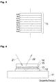
Fig. 3 is a sectional view schematically showing a configuration of an enhanced reflection layer. -
Fig. 4 is a sectional view schematically showing a configuration of a light emitting element of Comparative Example 1. -
Fig. 5 is a graph showing variation in illuminance when the element of Comparative Example 1 is irradiated with excitation light. -
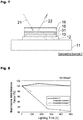
Fig. 6 is a sectional view schematically showing the appearance when the element of Comparative Example 1 is irradiated with excitation light having high intensity for a predetermined time. -
Fig. 7 is a sectional view schematically showing a configuration of a light emitting element of Comparative Example 2. -
Fig. 8 is a graph showing variation in illuminance when each element of Comparative Example 1, Comparative Example 2, and Example 1 is irradiated withexcitation light 21. -
Fig. 9 is a view schematically showing a conventional fluorescent light source device. - Referring to drawings, configurations of the light emitting element and the fluorescent light source device of the present invention will be described. In each of the following drawings, the depicted dimensional ratio is not necessarily coincident with the actual dimensional ratio.
-
Fig. 1 is a view schematically showing a configuration of one embodiment of a fluorescent light source device. A fluorescentlight source device 1 shown inFig. 1 includes anexcitation light source 2, adichroic mirror 3, and alight emitting element 10. - The
excitation light source 2 includes a semiconductor laser device that emits light in the blue region having a wavelength of 445 nm or more and 465 nm or less, for example. Theexcitation light source 2 may include an optical system such as a collimator lens as necessary. - The
light emitting element 10 includes a fluorescent body as will be described later. When thelight emitting element 10 is irradiated withexcitation light 21 emitted from theexcitation light source 2, the fluorescent body included in thelight emitting element 10 is excited, andfluorescence 22 is radiated from thelight emitting element 10. Thefluorescence 22 is light having a longer wavelength than theexcitation light 21, and has a wavelength of 470 nm or more and 700 nm or less, for example. - In the fluorescent
light source device 1 shown inFig. 1 , thedichroic mirror 3 is configured to transmit theexcitation light 21 emitted from theexcitation light source 2, while reflecting thefluorescence 22 emitted from thelight emitting element 10. Thedichroic mirror 3 is arranged so that the mirror surface is inclined at an angle of 45° to the incidence angle of theexcitation light 21, for example. With such a configuration, thefluorescence 22 is extracted outside the fluorescentlight source device 1, and enters a subsequent optical system (not shown), for example. - The optical arranging method of the fluorescent
light source device 1 including thedichroic mirror 3 as shown inFig. 1 is merely one example, and any arrangement form is possible. -
Fig. 2 is a sectional view schematically showing a configuration of thelight emitting element 10. As shown inFig. 2 , thelight emitting element 10 has asubstrate 11, abonding layer 12, areflection layer 13, adiffusion prevention layer 14, anenhanced reflection layer 15, and afluorescent body layer 16. - The
substrate 11 is provided for supporting thefluorescent body layer 16 and discharging the heat emitted in thefluorescent body layer 16. Thesubstrate 11 is formed of a material having a thermal conductivity of 90 W/(m- K) or more, specifically, 230 to 400 W/(m- K), for example. Examples of such a material include Cu, copper compounds (MoCu, CuW and the like), and Al. - The thickness of the
substrate 11 is, for example, 0.5 to 5 mm. From the viewpoint of heat discharge property or the like, it is preferred that the area in the surface of thesubstrate 11 be larger than the area of thefluorescent body layer 16. - The
bonding layer 12 is a layer for bonding thesubstrate 11, and other layer including thefluorescent body layer 16, and is formed, for example, of a solder material. From the viewpoint of heat discharge property or the like, it is preferred to use, for example, a material having a thermal conductivity of 40 W/(m·K) or more as a material forming thebonding layer 12. More specifically, for example, a cream solder prepared by mixing flux and other impurities with a material such as Sn, Pb and the like to give a creamy (pasty) state, an Sn-Ag-Cu solder, an Au-Sn solder and the like can be used. The thickness of thebonding layer 12 is, for example, 20 to 200 µm. - Although not illustrated, from the viewpoint of further improving the bonding property between the
substrate 11 and thebonding layer 12, a metal film of a Ni/Au film formed, for example, by plating may be formed between thesubstrate 11 and thebonding layer 12. The thickness of the metal film can be, for example, Ni/Au = 1000 to 5000 nm/30 to 1000 nm. - The
reflection layer 13 is formed on the upper layer of thebonding layer 12. Thereflection layer 13 is provided for reflecting fluorescence that has advanced on the surface opposite to the light extraction surface (on thesubstrate 11 side) of thefluorescent body layer 16 of thefluorescence 22 generated in thefluorescent body layer 16, and guiding the fluorescence to the light extraction surface side. Thereflection layer 13 is formed of a material having high reflectance (for example, 70% or more) for thefluorescence 22 generated in thefluorescent body layer 16, and is formed, for example, of metal consisting of Al or Ag, or a material film containing the metal. Preferably, thereflection layer 13 is formed of Ag. The thickness of thereflection layer 13 is, for example, 100 nm or more and 200 nm or less, and more preferably 120 nm or more and 180 nm or less. - Although not illustrated, from the viewpoint of further improving the adhesiveness between the
reflection layer 13 and thesubstrate 11, a metal film of a Ni/Pt/Au film or a Ni/Au film, formed, for example, by vapor deposition may be formed on a surface of thereflection layer 13 on thesubstrate 11 side. The thickness of the metal film can be, for example, Ni/Pt/Au = 30 nm/500 nm/500 nm. - The
diffusion prevention layer 14 is located between thereflection layer 13 and theenhanced reflection layer 15, and is formed in contact with a surface of thereflection layer 13 on the side opposite to thesubstrate 11. Thediffusion prevention layer 14 is formed of a layer that is at least partly crystallized, and is not amorphous. Thediffusion prevention layer 14 may be formed of a layer that is completely crystalized in the overall region. - As a method for analyzing the condition of crystallization of the
diffusion prevention layer 14, for example, a reflection high energy electron diffraction (RHEED) can be recited. A reflection high energy electron diffraction image of thediffusion prevention layer 14 that is partly crystalized shows a ring-like or a dotted pattern according to the crystal orientation. On the other hand, a reflection high energy electron diffraction image of an amorphous layer shows a halo-like (blurred ring-like) pattern. Therefore, the condition of the crystallization can be recognized according to the difference in shape of the reflection high energy electron diffraction image of the objective layer. - In the present embodiment, the
diffusion prevention layer 14 is formed of TiO2 that is at least partly crystalized. At least partial crystallization realizes the high density of thediffusion prevention layer 14. Specifically, the density of thediffusion prevention layer 14 is higher than 3.82 g/cm3, preferably 3.92 g/cm3 or more. The density of thediffusion prevention layer 14 can be determined from the relation between the refractive index and the density. The relation between the refractive index and the density is generally represented as a Lorentz equation, and is represented by the equation of r = [(n2 - 1)/(n2+ 2)] × (M/RD), wherein r (g/cm3) represents a density, n represents a refractive index, M represents a molecular weight (g/mol), and RD represents a molar reflective index (cm3/mol). - The
diffusion prevention layer 14 is not limited to TiO2, but may be formed of an oxide layer formed of Al2O3, SiO2, Ta2O5, ZrO2, or Nb2O5 and the like, a nitride layer formed of SiN or the like, or a fluoride layer formed of MgF2, CaF2 or the like. However, from the viewpoint of ensuring high adhesiveness with respect to thereflection layer 13 and theenhanced reflection layer 15, it is preferred that thediffusion prevention layer 14 be formed of an oxide layer. Further, from the viewpoint of ease of deposition of a layer having high crystallinity, it is particularly preferred that thediffusion prevention layer 14 be formed of TiO2. - Formation of the
diffusion prevention layer 14 that is at least partly crystallized can be realized by an EB-IAD method in which vapor deposition is conducted under irradiation with argon ion, for example. In general, for deposition of TiO2, vapor deposition using the EB method is generally used, and in this case, the deposited TiO2 is amorphous. - The thickness of the
diffusion prevention layer 14 is for example, 5 nm or more and 200 nm or less, more preferably 50 nm or more and 100 nm or less. - The
enhanced reflection layer 15 is formed in contact with a surface of thediffusion prevention layer 14 on the side opposite to thesubstrate 11. As shown inFig. 3 , theenhanced reflection layer 15 is an optical multilayer film in which a low refractive index material layer (Low) and a high refractive index material layer (High) are alternately laminated. The thickness of each layer constituting theenhanced reflection layer 15 is about 1/4 of the wavelength of thefluorescence 22, and is, for example, 5 nm or more and 200 nm or less, more preferably 50 nm or more and 100 nm or less. The overall thickness of theenhanced reflection layer 15 is 10 nm or more and 500 nm or less, more preferably 50 nm or more and 200 nm or less. - As a low refractive index material constituting the
enhanced reflection layer 15, for example, SiO2 (refractive index n = 1.45), Al2O3 (refractive index n = 1.63) or the like can be used. As a high refractive index material constituting theenhanced reflection layer 15, for example, TiO2 (refractive index n = 2.35), Nb2O5 (refractive index n = 2.37) or the like can be used. By sequentially depositing these materials by sputtering, vacuum vapor deposition or the like method, theenhanced reflection layer 15 is formed. - The layer constituting the
enhanced reflection layer 15 may be amorphous, or at least partly crystalized. It suffices that theenhanced reflection layer 15 is provided with at least one low refractive index material layer and at least one high refractive index material layer, and the lamination may be repeated two or more times. When the low refractive index material layer and the high refractive index material layer are laminated repeatedly, the film thickness of each low refractive index material layer and the film thickness of each high refractive index material layer are not necessarily identical. - The
fluorescent body layer 16 is formed on the upper layer of theenhanced reflection layer 15. Upon incidence of theexcitation light 21 emitted from theexcitation light source 2, thefluorescent body layer 16 generates and radiatesfluorescence 22. Thefluorescent body layer 16 assumes a rectangular plate-like structure, as one example. The thickness of thefluorescent body layer 16 is, for example, 0.05 to 1 mm. - The
fluorescent body layer 16 includes a fluorescent body. More specifically, thefluorescent body layer 16 is formed of a monocrystalline or polycrystalline fluorescent body, or a sintered body of a mixture of the fluorescent body and a ceramic binder. That is, thefluorescent body layer 16 is formed of a monocrystalline or polycrystalline fluorescent body. - In the sintered body of a mixture of a fluorescent body and a ceramic binder used in the
fluorescent body layer 16, for example, alumina particles of nano size are used as the ceramic binder. Then the sintered body can be obtained by mixing several % by mass to several tens % by mass of a ceramic binder with respect to 100% by mass of a fluorescent body, and pressing the mixture, followed by sintering. - When the
fluorescent body layer 16 is formed of a monocrystalline fluorescent body, for example, the fluorescent body can be obtained by the Czochralski method. To be more specific, a seed crystal is brought into contact with a material in a crucible, and in this condition, the seed crystal is pulled up in the vertical direction while the seed crystal is rotated to cause growth of a single crystal, and thus a fluorescent body of single crystal is obtained. - When the
fluorescent body layer 16 is formed of a polycrystalline fluorescent body, for example, the fluorescent body can be obtained, for example, in the following manner. First, raw materials such as a base material, an activating material and a baking auxiliary agent are ground by a ball mill or the like, to obtain raw material microparticles of submicron or smaller. Then, using the raw material microparticles, a molded body is formed, for example by a slip cast method, and sintered. Then, the obtained sintered body is subjected to a hot hydrostatic pressure process to obtain a polycrystalline fluorescent body having a porosity of, for example, 0.5 % or less. - As the fluorescent body constituting the
fluorescent body layer 16, specifically, a YAG fluorescent body doped (activated) with a rare earth compound can be used. In such a fluorescent body, the doping amount of the rare earth element (activating agent) can be about 0.5 mol%. Examples of the rare earth compound include Ce, Pr, and Sm. Concrete examples of the fluorescent body include YAG:Ce, YAG:Pr, YAG:Sm, and LuAG:Ce. Thefluorescent body layer 16 may contain a metal compound in the fluorescent body. - Hereinafter, the effect by the
light emitting element 1 of the present embodiment is shown by referring to Examples and Comparative Examples. The element corresponding to the above-described configuration of thelight emitting element 10 is referred to as Example 1. In Example 1, thediffusion prevention layer 14 is formed of TiO2 that is at least partly crystallized, and has a density of 3.92 g/cm3 and a refractive index of 2.45. Theenhanced reflection layer 15 is formed of a multilayer film including a plurality of sets of layers of SiO2/TiO2. The layers constituting theenhanced reflection layer 15 are amorphous. -
Fig. 4 is a view schematically showing a configuration of Comparative Example 1. Comparative Example 1 differs from Example 1 in that thediffusion prevention layer 14 is not provided. Thereflection layer 13 is in contact with theenhanced reflection layer 15. More specifically, the SiO2 layer included in theenhanced reflection layer 15 is in contact with thereflection layer 13. The SiO2 layer has a density of 2.2 g/cm3 and a refractive index of 1.45. -
Fig. 5 is a graph showing variation in illuminance when the element of Comparative Example 1 is irradiated with theexcitation light 21 emitted from theexcitation light source 2. InFig. 5 , three sets of data obtained by varying the maximum power density of theexcitation light 21 are shown. The maximum power density refers to the power density of the part where the power is the greatest on the surface of thefluorescent body layer 16 irradiated with theexcitation light 21. InFig. 5 , three cases where the maximum power density of theexcitation light 21 is 60 W/mm2, 80 W/mm2, and 100 W/mm2, respectively. - In
Fig. 5 , the horizontal axis indicates continuous irradiation time of theexcitation light 21, and the vertical axis indicates the illuminance maintenance factor. The illuminance maintenance factor refers the rate of illuminance relative to the illuminance in the initial stage of irradiation with theexcitation light 21 in each element. - According to
Fig. 5 , it is found that the illuminance maintenance factor drastically decreases in the case of a maximum power density of 100W/mm2, as compared with the cases of 60 W/mm2, and 80 W/mm2. As a result of analysis made by the present inventors, it was found that in the element of Comparative Example 1 after irradiation for 270 hours with theexcitation light 21 having a maximum power density of 100 W/mm2, amaterial layer 19 that is different from the material constituting theenhanced reflection layer 15 precipitated in theenhanced reflection layer 15 as schematically shown inFig. 6 . As a result of more specific investigation, it was confirmed that thematerial layer 19 is formed of a material containing Ag. - From this result, the present inventors inferred that by irradiation of the element of Comparative Example 1 with the
excitation light 21 having a high power density, Ag which is a material constituting thereflection layer 13 diffuses on theenhanced reflection layer 15 side, and decreases the reflectance and the transmittance in theenhanced reflection layer 15, and thus the illuminance decreases, as described above in "MEANS FOR SOLVING THE PROBLEMS". -
Fig. 7 is a view schematically showing a configuration of Comparative Example 2. Likewise Comparative Example 1, Comparative Example 2 does not have thediffusion prevention layer 14. Comparative Example 2 is different from Comparative Example 1 in that an Al2O3 layer 31 for improving the adhesiveness is provided between theenhanced reflection layer 15 and thereflection layer 13. The Al2O3 layer 31 is in contact with the SiO2 layer contained in theenhanced reflection layer 15 and thereflection layer 13. The Al2O3 layer 31 has a density of 3.25 g/cm3, and a refractive index of 1.63. -
Fig. 8 is a graph showing variation in illuminance when each element of Comparative Example 1, Comparative Example 2 and Example 1 is irradiated with theexcitation light 21 emitted from theexcitation light source 2 at a maximum power density of 100 W/mm2. The data of Comparative Example 1 is the same as the data at 100 W/mm2 inFig. 5 . - According to
Fig. 8 , also in the element of Comparative Example 2, it is found that the illuminance starts decreasing largely directly after start of the irradiation. More specifically, both in the element of Comparative Example 1 and the element of Comparative Example 2, it is found that the illuminance decreases to about 98% after a lapse of about 100 hours from start of illumination. In contrast to this, in the element of Example 1, it is found that approximately 100% of illuminance is maintained after a lapse of 500 hours. - While Comparative Example 2 lacks data after a lapse of 100 hours or more in
Fig. 8 , it is hard to imagine that the illuminance shows the rising trend after 100 hours or later, and it is expected that the illuminance continually decreases with the lapse of time by referring to the data of Comparative Example 1. - Although not shown in the graph, the same verification was conducted for the element in which the TiO2 layer included in the
enhanced reflection layer 15 is brought into contact with thereflection layer 13 in the element of Comparative Example 1 (hereinafter, referred to as "Comparative Example 3"), and also in this case, the illuminance maintenance factor decreased to about 98% after a lapse of about 100 hours as is the case with Comparative Example 1 or Comparative Example 2. The TiO2 layer included in theenhanced reflection layer 15 is amorphous as described above, and has a density of 3.82 g/cm3 and a refractive index of 2.35. - According to the above verification, in each of Comparative Examples 1 to 3, the density of the layer being in contact with the upper surface of the
reflection layer 13 is low, and a large number of dangling bonds exist, so that Ag ions constituting thereflection layer 13 are attracted to the dangling bonds. This would result in diffusion of the material containing Ag in theenhanced reflection layer 15 to decrease the illuminance maintenance factor. On the other hand, according to the element of Example 1, since thediffusion prevention layer 14 having high density is in contact with the upper surface of thereflection layer 13, Ag ions cannot easily diffuse in thediffusion prevention layer 14, and this would result in prevention of advance into theenhanced reflection layer 15. The above verification reveals that the density of thediffusion prevention layer 14 formed in contact with the upper surface of thereflection layer 13 is preferably more than 3.82 g/cm3, and more preferably 3.92 g/cm3 or more. - According to the above verification result, the
diffusion prevention layer 14 may be a layer having high crystallinity and high density, and more preferably a layer in a complete crystalline state. Thediffusion prevention layer 14 realizes the function of preventing diffusion of Ag ions even when it is partly crystallized, in comparison with an amorphous layer. Therefore, it is possible to suppress decrease in illuminance in the case of irradiation with excitation light having high intensity. - In the above-described embodiment, the case where the
reflection layer 13 is formed of Ag has been described, it is inferred that the effect is realized also in the case where thereflection layer 13 is formed of Al for the same reason. The same applies also to the case where thereflection layer 13 is formed of a metal material containing Ag, Al. -
- 1
- Fluorescent light source device
- 2
- Excitation light source
- 3
- Dichroic mirror
- 10
- Light emitting element
- 11
- Substrate
- 12
- Bonding layer
- 13
- Reflection layer
- 14
- Diffusion prevention layer
- 15
- Enhanced reflection layer
- 16
- Fluorescent body layer
- 19
- Material layer containing Ag
- 21
- Excitation light
- 22
- Fluorescence
- 31
- Al2O3 layer
- 100
- Conventional fluorescent light source device
- 110
- Excitation light source
- 120
- Conventional light emitting element
- 121
- Substrate
- 122
- Bonding layer
- 123
- Reflection layer
- 124
- Enhanced reflection layer
- 125
- Total reflection layer
- 126
- Fluorescent body layer
- 131
- Excitation light
- 132
- Fluorescence
Claims (15)
- A light emitting element comprising:a substrate;a reflection layer formed of a material containing Ag or Al, formed on the upper layer of the substrate;a diffusion prevention layer formed of a layer at least part of which being crystallized, the diffusion prevention layer being formed in contact with a surface of the reflection layer on a side opposite to the substrate,an enhanced reflection layer formed in contact with a surface of the diffusion prevention layer on a side opposite to the substrate; anda fluorescent body layer formed on the upper layer of the enhanced reflection layer.
- The light emitting element according to claim 1, wherein the diffusion prevention layer has a density of more than 3.82 g/cm3.
- The light emitting element according to claim 2, wherein the diffusion prevention layer is formed of an oxide layer.
- The light emitting element according to claim 3, wherein the diffusion prevention layer is formed of TiO2.
- The light emitting element according to claim 4, wherein the diffusion prevention layer has a thickness of 5 nm or more and 200 nm or less.
- A fluorescent light source device comprising:the light emitting element according to claim 1; andan excitation light source that irradiates a first surface on a farther side from the substrate of surfaces of the fluorescent body layer with excitation light, whereinthe fluorescent body layer radiates fluorescence having a longer wavelength than the excitation light from the first surface upon incidence of the excitation light.
- A fluorescent light source device comprising:the light emitting element according to claim 2; andan excitation light source that irradiates a first surface on a farther side from the substrate of surfaces of the fluorescent body layer with excitation light, whereinthe fluorescent body layer radiates fluorescence having a longer wavelength than the excitation light from the first layer upon incidence of the excitation light.
- A fluorescent light source device comprising:the light emitting element according to claim 3; andan excitation light source that irradiates a first surface on a farther side from the substrate of surfaces of the fluorescent body layer with excitation light, whereinthe fluorescent body layer radiates fluorescence having a longer wavelength than the excitation light from the first layer upon incidence of the excitation light.
- A fluorescent light source device comprising:the light emitting element according to claim 4; andan excitation light source that irradiates a first surface on a farther side from the substrate of surfaces of the fluorescent body layer with excitation light, whereinthe fluorescent body layer radiates fluorescence having a longer wavelength than the excitation light from the first layer upon incidence of the excitation light.
- A fluorescent light source device comprising:the light emitting element according to claim 5; andan excitation light source that irradiates a first surface on a farther side from the substrate of surfaces of the fluorescent body layer with excitation light, whereinthe fluorescent body layer radiates fluorescence having a longer wavelength than the excitation light from the first layer upon incidence of the excitation light.
- The fluorescent light source device according to claim 6, wherein the excitation light source is a light source capable of emitting the excitation light having a maximum power density on the first surface of 100 W/mm2 or more.
- The fluorescent light source device according to claim 7, wherein the excitation light source is a light source capable of emitting the excitation light having a maximum power density on the first surface of 100 W/mm2 or more.
- The fluorescent light source device according to claim 8, wherein the excitation light source is a light source capable of emitting the excitation light having a maximum power density on the first surface of 100 W/mm2 or more.
- The fluorescent light source device according to claim 9, wherein the excitation light source is a light source capable of emitting the excitation light having a maximum power density on the first surface of 100 W/mm2 or more.
- The fluorescent light source device according to claim 10, wherein the excitation light source is a light source capable of emitting the excitation light having a maximum power density on the first surface of 100 W/mm2 or more.
Applications Claiming Priority (2)
| Application Number | Priority Date | Filing Date | Title |
|---|---|---|---|
| JP2017008872A JP6361995B2 (en) | 2017-01-20 | 2017-01-20 | Light emitting element, fluorescent light source device |
| PCT/JP2018/000289 WO2018135345A1 (en) | 2017-01-20 | 2018-01-10 | Light emitting element, fluorescent light source device |
Publications (3)
| Publication Number | Publication Date |
|---|---|
| EP3572725A1 true EP3572725A1 (en) | 2019-11-27 |
| EP3572725A4 EP3572725A4 (en) | 2020-02-19 |
| EP3572725B1 EP3572725B1 (en) | 2021-07-07 |
Family
ID=62908616
Family Applications (1)
| Application Number | Title | Priority Date | Filing Date |
|---|---|---|---|
| EP18741463.6A Active EP3572725B1 (en) | 2017-01-20 | 2018-01-10 | Light emitting element, fluorescent light source device |
Country Status (5)
| Country | Link |
|---|---|
| US (1) | US10711975B2 (en) |
| EP (1) | EP3572725B1 (en) |
| JP (1) | JP6361995B2 (en) |
| CN (1) | CN110168279B (en) |
| WO (1) | WO2018135345A1 (en) |
Families Citing this family (5)
| Publication number | Priority date | Publication date | Assignee | Title |
|---|---|---|---|---|
| JP7357082B2 (en) * | 2020-02-07 | 2023-10-05 | スタンレー電気株式会社 | Optical device and optical device manufacturing method |
| JP7535780B2 (en) * | 2020-09-18 | 2024-08-19 | 株式会社オキサイド | Light emitting devices and light source devices |
| KR102873963B1 (en) * | 2021-01-28 | 2025-10-20 | 니혼도꾸슈도교 가부시키가이샤 | Wavelength conversion member and light source device having the same |
| TWI854471B (en) * | 2022-10-28 | 2024-09-01 | 台達電子工業股份有限公司 | Optical wavelength conversion structure |
| CN117734250A (en) * | 2023-12-29 | 2024-03-22 | 广州光联电子科技有限公司 | Reflective wavelength conversion device |
Family Cites Families (12)
| Publication number | Priority date | Publication date | Assignee | Title |
|---|---|---|---|---|
| US6027766A (en) | 1997-03-14 | 2000-02-22 | Ppg Industries Ohio, Inc. | Photocatalytically-activated self-cleaning article and method of making same |
| EP1426941A4 (en) * | 2001-09-13 | 2008-08-27 | Tdk Corp | Optical recording medium |
| JP4106417B2 (en) * | 2002-05-16 | 2008-06-25 | 三星電子株式会社 | Recording medium having a high melting point recording layer, information recording method for the recording medium, information reproducing apparatus and information reproducing method for reproducing information from the recording medium |
| TWI242606B (en) * | 2003-09-26 | 2005-11-01 | Optomec Design | Laser treatment process for maskless low-temperature deposition of electronic materials |
| US7732229B2 (en) * | 2004-09-18 | 2010-06-08 | Nanosolar, Inc. | Formation of solar cells with conductive barrier layers and foil substrates |
| KR101895421B1 (en) | 2011-02-24 | 2018-09-07 | 삼성디스플레이 주식회사 | Wiring, thin film transistor, thin film transistor panel and methods for manufacturing the same |
| JP2014137973A (en) * | 2013-01-18 | 2014-07-28 | Stanley Electric Co Ltd | Light source device |
| JP2015050124A (en) * | 2013-09-03 | 2015-03-16 | スタンレー電気株式会社 | Light emitting device |
| JP2016061852A (en) * | 2014-09-16 | 2016-04-25 | セイコーエプソン株式会社 | Wavelength conversion element, light source device, and projector |
| JP6371201B2 (en) * | 2014-11-18 | 2018-08-08 | スタンレー電気株式会社 | Light emitting module and light emitting device using the same |
| JP6094617B2 (en) * | 2015-03-31 | 2017-03-15 | ウシオ電機株式会社 | Fluorescent light source device |
| DE112017003014B4 (en) * | 2016-06-16 | 2025-03-06 | Ngk Insulators, Ltd. | phosphor device and fluorescence-emitting lighting device |
-
2017
- 2017-01-20 JP JP2017008872A patent/JP6361995B2/en active Active
-
2018
- 2018-01-10 US US16/477,797 patent/US10711975B2/en active Active
- 2018-01-10 CN CN201880005992.3A patent/CN110168279B/en active Active
- 2018-01-10 EP EP18741463.6A patent/EP3572725B1/en active Active
- 2018-01-10 WO PCT/JP2018/000289 patent/WO2018135345A1/en not_active Ceased
Also Published As
| Publication number | Publication date |
|---|---|
| EP3572725A4 (en) | 2020-02-19 |
| WO2018135345A1 (en) | 2018-07-26 |
| US10711975B2 (en) | 2020-07-14 |
| US20200124251A1 (en) | 2020-04-23 |
| CN110168279A (en) | 2019-08-23 |
| JP6361995B2 (en) | 2018-07-25 |
| CN110168279B (en) | 2021-01-08 |
| JP2018116911A (en) | 2018-07-26 |
| EP3572725B1 (en) | 2021-07-07 |
Similar Documents
| Publication | Publication Date | Title |
|---|---|---|
| EP3572725B1 (en) | Light emitting element, fluorescent light source device | |
| RU2479072C2 (en) | Light-emitting device having photonic crystal and luminescent ceramic | |
| US9785039B2 (en) | Wavelength conversion member, light emitting device, projector, and method of manufacturing wavelength conversion member | |
| US7285791B2 (en) | Wavelength conversion chip for use in solid-state lighting and method for making same | |
| US20100308361A1 (en) | Wavelength conversion chip for use with light emitting diodes and method for making same | |
| US10139055B2 (en) | Fluorescence light source device with periodic structure having an aspect ratio of 0.5 to 0.9 and method for producing the same | |
| JP2009522713A (en) | Processing structure for solid state light emitters | |
| WO2012012354A2 (en) | Full spectrum solid state white light source, method for manufacturing and applications | |
| JP2015526368A (en) | Multilayer substrate structure and manufacturing method and system thereof | |
| JPH05335622A (en) | Semiconductor light emitting device | |
| CN111051933A (en) | Wavelength conversion member, light source, lighting device, and method for manufacturing wavelength conversion member | |
| WO2019181478A1 (en) | Wavelength conversion member and wavelength conversion element | |
| TWI314788B (en) | Thin-film semiconductor-body | |
| JP2015179599A (en) | fluorescent light source device | |
| US11105486B2 (en) | Optic and illumination device | |
| JP7157898B2 (en) | Wavelength conversion member | |
| JP2016178087A (en) | Fluorescent light source device | |
| JP6747285B2 (en) | Light emitting device, fluorescent light source device | |
| WO2017175635A1 (en) | Fluorescent light source device | |
| Soshchin et al. | A Cathodoluminescent Screen of Columnar Structure for Field Emission Displays | |
| COETZEE | Philosophiae Doctor |
Legal Events
| Date | Code | Title | Description |
|---|---|---|---|
| STAA | Information on the status of an ep patent application or granted ep patent |
Free format text: STATUS: THE INTERNATIONAL PUBLICATION HAS BEEN MADE |
|
| PUAI | Public reference made under article 153(3) epc to a published international application that has entered the european phase |
Free format text: ORIGINAL CODE: 0009012 |
|
| STAA | Information on the status of an ep patent application or granted ep patent |
Free format text: STATUS: REQUEST FOR EXAMINATION WAS MADE |
|
| 17P | Request for examination filed |
Effective date: 20190730 |
|
| AK | Designated contracting states |
Kind code of ref document: A1 Designated state(s): AL AT BE BG CH CY CZ DE DK EE ES FI FR GB GR HR HU IE IS IT LI LT LU LV MC MK MT NL NO PL PT RO RS SE SI SK SM TR |
|
| AX | Request for extension of the european patent |
Extension state: BA ME |
|
| A4 | Supplementary search report drawn up and despatched |
Effective date: 20200122 |
|
| RIC1 | Information provided on ipc code assigned before grant |
Ipc: F21V 7/30 20180101ALI20200116BHEP Ipc: G02B 5/20 20060101ALI20200116BHEP Ipc: F21V 9/30 20180101ALI20200116BHEP Ipc: F21V 7/26 20180101ALI20200116BHEP Ipc: F21Y 115/30 20160101ALI20200116BHEP Ipc: F21V 7/28 20180101ALI20200116BHEP Ipc: F21V 7/24 20180101AFI20200116BHEP Ipc: G02B 5/08 20060101ALI20200116BHEP |
|
| DAV | Request for validation of the european patent (deleted) | ||
| DAX | Request for extension of the european patent (deleted) | ||
| GRAP | Despatch of communication of intention to grant a patent |
Free format text: ORIGINAL CODE: EPIDOSNIGR1 |
|
| STAA | Information on the status of an ep patent application or granted ep patent |
Free format text: STATUS: GRANT OF PATENT IS INTENDED |
|
| INTG | Intention to grant announced |
Effective date: 20210303 |
|
| GRAS | Grant fee paid |
Free format text: ORIGINAL CODE: EPIDOSNIGR3 |
|
| GRAA | (expected) grant |
Free format text: ORIGINAL CODE: 0009210 |
|
| STAA | Information on the status of an ep patent application or granted ep patent |
Free format text: STATUS: THE PATENT HAS BEEN GRANTED |
|
| AK | Designated contracting states |
Kind code of ref document: B1 Designated state(s): AL AT BE BG CH CY CZ DE DK EE ES FI FR GB GR HR HU IE IS IT LI LT LU LV MC MK MT NL NO PL PT RO RS SE SI SK SM TR |
|
| REG | Reference to a national code |
Ref country code: GB Ref legal event code: FG4D |
|
| REG | Reference to a national code |
Ref country code: AT Ref legal event code: REF Ref document number: 1408943 Country of ref document: AT Kind code of ref document: T Effective date: 20210715 |
|
| REG | Reference to a national code |
Ref country code: DE Ref legal event code: R096 Ref document number: 602018019784 Country of ref document: DE |
|
| REG | Reference to a national code |
Ref country code: IE Ref legal event code: FG4D |
|
| REG | Reference to a national code |
Ref country code: LT Ref legal event code: MG9D |
|
| REG | Reference to a national code |
Ref country code: NL Ref legal event code: MP Effective date: 20210707 |
|
| REG | Reference to a national code |
Ref country code: AT Ref legal event code: MK05 Ref document number: 1408943 Country of ref document: AT Kind code of ref document: T Effective date: 20210707 |
|
| PG25 | Lapsed in a contracting state [announced via postgrant information from national office to epo] |
Ref country code: SE Free format text: LAPSE BECAUSE OF FAILURE TO SUBMIT A TRANSLATION OF THE DESCRIPTION OR TO PAY THE FEE WITHIN THE PRESCRIBED TIME-LIMIT Effective date: 20210707 Ref country code: RS Free format text: LAPSE BECAUSE OF FAILURE TO SUBMIT A TRANSLATION OF THE DESCRIPTION OR TO PAY THE FEE WITHIN THE PRESCRIBED TIME-LIMIT Effective date: 20210707 Ref country code: HR Free format text: LAPSE BECAUSE OF FAILURE TO SUBMIT A TRANSLATION OF THE DESCRIPTION OR TO PAY THE FEE WITHIN THE PRESCRIBED TIME-LIMIT Effective date: 20210707 Ref country code: ES Free format text: LAPSE BECAUSE OF FAILURE TO SUBMIT A TRANSLATION OF THE DESCRIPTION OR TO PAY THE FEE WITHIN THE PRESCRIBED TIME-LIMIT Effective date: 20210707 Ref country code: FI Free format text: LAPSE BECAUSE OF FAILURE TO SUBMIT A TRANSLATION OF THE DESCRIPTION OR TO PAY THE FEE WITHIN THE PRESCRIBED TIME-LIMIT Effective date: 20210707 Ref country code: NL Free format text: LAPSE BECAUSE OF FAILURE TO SUBMIT A TRANSLATION OF THE DESCRIPTION OR TO PAY THE FEE WITHIN THE PRESCRIBED TIME-LIMIT Effective date: 20210707 Ref country code: PT Free format text: LAPSE BECAUSE OF FAILURE TO SUBMIT A TRANSLATION OF THE DESCRIPTION OR TO PAY THE FEE WITHIN THE PRESCRIBED TIME-LIMIT Effective date: 20211108 Ref country code: NO Free format text: LAPSE BECAUSE OF FAILURE TO SUBMIT A TRANSLATION OF THE DESCRIPTION OR TO PAY THE FEE WITHIN THE PRESCRIBED TIME-LIMIT Effective date: 20211007 Ref country code: LT Free format text: LAPSE BECAUSE OF FAILURE TO SUBMIT A TRANSLATION OF THE DESCRIPTION OR TO PAY THE FEE WITHIN THE PRESCRIBED TIME-LIMIT Effective date: 20210707 Ref country code: BG Free format text: LAPSE BECAUSE OF FAILURE TO SUBMIT A TRANSLATION OF THE DESCRIPTION OR TO PAY THE FEE WITHIN THE PRESCRIBED TIME-LIMIT Effective date: 20211007 Ref country code: AT Free format text: LAPSE BECAUSE OF FAILURE TO SUBMIT A TRANSLATION OF THE DESCRIPTION OR TO PAY THE FEE WITHIN THE PRESCRIBED TIME-LIMIT Effective date: 20210707 |
|
| PG25 | Lapsed in a contracting state [announced via postgrant information from national office to epo] |
Ref country code: PL Free format text: LAPSE BECAUSE OF FAILURE TO SUBMIT A TRANSLATION OF THE DESCRIPTION OR TO PAY THE FEE WITHIN THE PRESCRIBED TIME-LIMIT Effective date: 20210707 Ref country code: LV Free format text: LAPSE BECAUSE OF FAILURE TO SUBMIT A TRANSLATION OF THE DESCRIPTION OR TO PAY THE FEE WITHIN THE PRESCRIBED TIME-LIMIT Effective date: 20210707 Ref country code: GR Free format text: LAPSE BECAUSE OF FAILURE TO SUBMIT A TRANSLATION OF THE DESCRIPTION OR TO PAY THE FEE WITHIN THE PRESCRIBED TIME-LIMIT Effective date: 20211008 |
|
| REG | Reference to a national code |
Ref country code: DE Ref legal event code: R097 Ref document number: 602018019784 Country of ref document: DE |
|
| PG25 | Lapsed in a contracting state [announced via postgrant information from national office to epo] |
Ref country code: DK Free format text: LAPSE BECAUSE OF FAILURE TO SUBMIT A TRANSLATION OF THE DESCRIPTION OR TO PAY THE FEE WITHIN THE PRESCRIBED TIME-LIMIT Effective date: 20210707 |
|
| PLBE | No opposition filed within time limit |
Free format text: ORIGINAL CODE: 0009261 |
|
| STAA | Information on the status of an ep patent application or granted ep patent |
Free format text: STATUS: NO OPPOSITION FILED WITHIN TIME LIMIT |
|
| PG25 | Lapsed in a contracting state [announced via postgrant information from national office to epo] |
Ref country code: SM Free format text: LAPSE BECAUSE OF FAILURE TO SUBMIT A TRANSLATION OF THE DESCRIPTION OR TO PAY THE FEE WITHIN THE PRESCRIBED TIME-LIMIT Effective date: 20210707 Ref country code: SK Free format text: LAPSE BECAUSE OF FAILURE TO SUBMIT A TRANSLATION OF THE DESCRIPTION OR TO PAY THE FEE WITHIN THE PRESCRIBED TIME-LIMIT Effective date: 20210707 Ref country code: RO Free format text: LAPSE BECAUSE OF FAILURE TO SUBMIT A TRANSLATION OF THE DESCRIPTION OR TO PAY THE FEE WITHIN THE PRESCRIBED TIME-LIMIT Effective date: 20210707 Ref country code: EE Free format text: LAPSE BECAUSE OF FAILURE TO SUBMIT A TRANSLATION OF THE DESCRIPTION OR TO PAY THE FEE WITHIN THE PRESCRIBED TIME-LIMIT Effective date: 20210707 Ref country code: CZ Free format text: LAPSE BECAUSE OF FAILURE TO SUBMIT A TRANSLATION OF THE DESCRIPTION OR TO PAY THE FEE WITHIN THE PRESCRIBED TIME-LIMIT Effective date: 20210707 Ref country code: AL Free format text: LAPSE BECAUSE OF FAILURE TO SUBMIT A TRANSLATION OF THE DESCRIPTION OR TO PAY THE FEE WITHIN THE PRESCRIBED TIME-LIMIT Effective date: 20210707 |
|
| 26N | No opposition filed |
Effective date: 20220408 |
|
| PG25 | Lapsed in a contracting state [announced via postgrant information from national office to epo] |
Ref country code: IT Free format text: LAPSE BECAUSE OF FAILURE TO SUBMIT A TRANSLATION OF THE DESCRIPTION OR TO PAY THE FEE WITHIN THE PRESCRIBED TIME-LIMIT Effective date: 20210707 |
|
| PG25 | Lapsed in a contracting state [announced via postgrant information from national office to epo] |
Ref country code: MC Free format text: LAPSE BECAUSE OF FAILURE TO SUBMIT A TRANSLATION OF THE DESCRIPTION OR TO PAY THE FEE WITHIN THE PRESCRIBED TIME-LIMIT Effective date: 20210707 |
|
| REG | Reference to a national code |
Ref country code: CH Ref legal event code: PL |
|
| GBPC | Gb: european patent ceased through non-payment of renewal fee |
Effective date: 20220110 |
|
| REG | Reference to a national code |
Ref country code: BE Ref legal event code: MM Effective date: 20220131 |
|
| PG25 | Lapsed in a contracting state [announced via postgrant information from national office to epo] |
Ref country code: LU Free format text: LAPSE BECAUSE OF NON-PAYMENT OF DUE FEES Effective date: 20220110 Ref country code: GB Free format text: LAPSE BECAUSE OF NON-PAYMENT OF DUE FEES Effective date: 20220110 |
|
| PG25 | Lapsed in a contracting state [announced via postgrant information from national office to epo] |
Ref country code: FR Free format text: LAPSE BECAUSE OF NON-PAYMENT OF DUE FEES Effective date: 20220131 Ref country code: BE Free format text: LAPSE BECAUSE OF NON-PAYMENT OF DUE FEES Effective date: 20220131 |
|
| PG25 | Lapsed in a contracting state [announced via postgrant information from national office to epo] |
Ref country code: LI Free format text: LAPSE BECAUSE OF NON-PAYMENT OF DUE FEES Effective date: 20220131 Ref country code: CH Free format text: LAPSE BECAUSE OF NON-PAYMENT OF DUE FEES Effective date: 20220131 |
|
| PG25 | Lapsed in a contracting state [announced via postgrant information from national office to epo] |
Ref country code: IE Free format text: LAPSE BECAUSE OF NON-PAYMENT OF DUE FEES Effective date: 20220110 |
|
| PG25 | Lapsed in a contracting state [announced via postgrant information from national office to epo] |
Ref country code: MK Free format text: LAPSE BECAUSE OF FAILURE TO SUBMIT A TRANSLATION OF THE DESCRIPTION OR TO PAY THE FEE WITHIN THE PRESCRIBED TIME-LIMIT Effective date: 20210707 Ref country code: CY Free format text: LAPSE BECAUSE OF FAILURE TO SUBMIT A TRANSLATION OF THE DESCRIPTION OR TO PAY THE FEE WITHIN THE PRESCRIBED TIME-LIMIT Effective date: 20210707 |
|
| PG25 | Lapsed in a contracting state [announced via postgrant information from national office to epo] |
Ref country code: HU Free format text: LAPSE BECAUSE OF FAILURE TO SUBMIT A TRANSLATION OF THE DESCRIPTION OR TO PAY THE FEE WITHIN THE PRESCRIBED TIME-LIMIT; INVALID AB INITIO Effective date: 20180110 |
|
| PG25 | Lapsed in a contracting state [announced via postgrant information from national office to epo] |
Ref country code: TR Free format text: LAPSE BECAUSE OF FAILURE TO SUBMIT A TRANSLATION OF THE DESCRIPTION OR TO PAY THE FEE WITHIN THE PRESCRIBED TIME-LIMIT Effective date: 20210707 |
|
| PG25 | Lapsed in a contracting state [announced via postgrant information from national office to epo] |
Ref country code: MT Free format text: LAPSE BECAUSE OF FAILURE TO SUBMIT A TRANSLATION OF THE DESCRIPTION OR TO PAY THE FEE WITHIN THE PRESCRIBED TIME-LIMIT Effective date: 20210707 |
|
| PGFP | Annual fee paid to national office [announced via postgrant information from national office to epo] |
Ref country code: DE Payment date: 20251203 Year of fee payment: 9 |