EP3570438A1 - Signal processing circuit - Google Patents
Signal processing circuit Download PDFInfo
- Publication number
- EP3570438A1 EP3570438A1 EP19162041.8A EP19162041A EP3570438A1 EP 3570438 A1 EP3570438 A1 EP 3570438A1 EP 19162041 A EP19162041 A EP 19162041A EP 3570438 A1 EP3570438 A1 EP 3570438A1
- Authority
- EP
- European Patent Office
- Prior art keywords
- resistive element
- stage circuit
- input terminal
- circuit
- signal processing
- Prior art date
- Legal status (The legal status is an assumption and is not a legal conclusion. Google has not performed a legal analysis and makes no representation as to the accuracy of the status listed.)
- Granted
Links
Images


Classifications
-
- H—ELECTRICITY
- H03—ELECTRONIC CIRCUITRY
- H03F—AMPLIFIERS
- H03F3/00—Amplifiers with only discharge tubes or only semiconductor devices as amplifying elements
- H03F3/45—Differential amplifiers
- H03F3/45071—Differential amplifiers with semiconductor devices only
- H03F3/45076—Differential amplifiers with semiconductor devices only characterised by the way of implementation of the active amplifying circuit in the differential amplifier
- H03F3/45475—Differential amplifiers with semiconductor devices only characterised by the way of implementation of the active amplifying circuit in the differential amplifier using IC blocks as the active amplifying circuit
-
- H—ELECTRICITY
- H03—ELECTRONIC CIRCUITRY
- H03M—CODING; DECODING; CODE CONVERSION IN GENERAL
- H03M1/00—Analogue/digital conversion; Digital/analogue conversion
- H03M1/06—Continuously compensating for, or preventing, undesired influence of physical parameters
- H03M1/0602—Continuously compensating for, or preventing, undesired influence of physical parameters of deviations from the desired transfer characteristic
- H03M1/0604—Continuously compensating for, or preventing, undesired influence of physical parameters of deviations from the desired transfer characteristic at one point, i.e. by adjusting a single reference value, e.g. bias or gain error
- H03M1/0607—Offset or drift compensation
-
- H—ELECTRICITY
- H03—ELECTRONIC CIRCUITRY
- H03F—AMPLIFIERS
- H03F3/00—Amplifiers with only discharge tubes or only semiconductor devices as amplifying elements
- H03F3/45—Differential amplifiers
-
- H—ELECTRICITY
- H03—ELECTRONIC CIRCUITRY
- H03H—IMPEDANCE NETWORKS, e.g. RESONANT CIRCUITS; RESONATORS
- H03H11/00—Networks using active elements
- H03H11/02—Multiple-port networks
- H03H11/04—Frequency selective two-port networks
- H03H11/0422—Frequency selective two-port networks using transconductance amplifiers, e.g. gmC filters
- H03H11/0455—Multiple integrator loop feedback filters
-
- H—ELECTRICITY
- H03—ELECTRONIC CIRCUITRY
- H03M—CODING; DECODING; CODE CONVERSION IN GENERAL
- H03M1/00—Analogue/digital conversion; Digital/analogue conversion
- H03M1/06—Continuously compensating for, or preventing, undesired influence of physical parameters
- H03M1/08—Continuously compensating for, or preventing, undesired influence of physical parameters of noise
-
- H—ELECTRICITY
- H03—ELECTRONIC CIRCUITRY
- H03F—AMPLIFIERS
- H03F2200/00—Indexing scheme relating to amplifiers
- H03F2200/411—Indexing scheme relating to amplifiers the output amplifying stage of an amplifier comprising two power stages
-
- H—ELECTRICITY
- H03—ELECTRONIC CIRCUITRY
- H03F—AMPLIFIERS
- H03F2203/00—Indexing scheme relating to amplifiers with only discharge tubes or only semiconductor devices as amplifying elements covered by H03F3/00
- H03F2203/45—Indexing scheme relating to differential amplifiers
- H03F2203/45134—Indexing scheme relating to differential amplifiers the whole differential amplifier together with other coupled stages being fully differential realised
-
- H—ELECTRICITY
- H03—ELECTRONIC CIRCUITRY
- H03F—AMPLIFIERS
- H03F2203/00—Indexing scheme relating to amplifiers with only discharge tubes or only semiconductor devices as amplifying elements covered by H03F3/00
- H03F2203/45—Indexing scheme relating to differential amplifiers
- H03F2203/45138—Two or more differential amplifiers in IC-block form are combined, e.g. measuring amplifiers
-
- H—ELECTRICITY
- H03—ELECTRONIC CIRCUITRY
- H03H—IMPEDANCE NETWORKS, e.g. RESONANT CIRCUITS; RESONATORS
- H03H11/00—Networks using active elements
- H03H11/02—Multiple-port networks
- H03H11/04—Frequency selective two-port networks
- H03H11/12—Frequency selective two-port networks using amplifiers with feedback
- H03H11/1291—Current or voltage controlled filters
-
- H—ELECTRICITY
- H03—ELECTRONIC CIRCUITRY
- H03M—CODING; DECODING; CODE CONVERSION IN GENERAL
- H03M1/00—Analogue/digital conversion; Digital/analogue conversion
- H03M1/12—Analogue/digital converters
- H03M1/124—Sampling or signal conditioning arrangements specially adapted for A/D converters
Definitions
- the disclosure relates to a signal processing circuit that performs AD conversion (analog-to-digital conversion).
- Patent Document 1 discloses a configuration using a differential amplifier for AD conversion of a differential input signal.
- Patent Document 1 Japanese Laid-open No. 2006-20171 (published on January 19, 2006 )
- Patent Document 1 has a poor noise removing effect with which it is not possible to address increasing an input range and a resolution.
- a signal processing circuit includes: a first pre-stage circuit that includes a first input terminal for receiving one of differential input; a second pre-stage circuit that includes a second input terminal for receiving another one of the differential input; a post-stage circuit that includes a differential output amplifier; and an analog-to-digital conversion circuit that is connected to the post-stage circuit.
- the first pre-stage circuit includes a first resistive element with one end connected to the first input terminal and a first capacitative element with one grounded electrode. The other end of the first resistive element and the other electrode of the first capacitative element are connected to each other.
- An output node of the first pre-stage circuit and an output node of the second pre-stage circuit are connected to the post-stage circuit.
- the post-stage circuit may include a second resistive element with one end connected to a negative output terminal of the differential output amplifier and a second capacitative element with one grounded electrode. The other end of the second resistive element, the other electrode of the second capacitative element, and one of two input terminals of the analog-to-digital conversion circuit may be connected to each other.
- Circuit configurations of the first pre-stage circuit and the second pre-stage circuit may be the same.
- the second pre-stage circuit may include a third resistive element with one end connected to the second input terminal and a third capacitative element with one grounded electrode. The other end of the third resistive element and the other electrode of the third capacitative element may be connected to each other.
- the post-stage circuit may include a fourth resistive element with one end connected to a positive output terminal of the differential output amplifier and a fourth capacitative element with one grounded electrode.
- the other end of the fourth resistive element, the other electrode of the fourth capacitative element, and the other of the two input terminals of the analog-to-digital conversion circuit may be connected to each other.
- the negative output terminal and a positive input terminal of the differential output amplifier may be connected via a fifth resistive element, and the positive output terminal and a negative input terminal of the differential output amplifier may be connected via a sixth resistive element.
- Resistance values of the first resistive element and the third resistive element may be the same, resistance values of the second resistive element and the fourth resistive element may be the same, capacitance values of the first capacitative element and the third capacitative element may be the same, and capacitative values of the second capacitative element and the fourth capacitative element may be the same.
- the output node of the first pre-stage circuit may be connected to the positive input terminal of the differential output amplifier via a seventh resistive element, and the output node of the second pre-stage circuit may be connected to the negative input terminal of the differential output amplifier via an eighth resistive element.
- the first pre-stage circuit and the second pre-stage circuit may be connected to each other via a fifth capacitative element.
- Analog signals from an external device may be supplied to the first input terminal and the second input terminal.
- FIG. 1 is a block diagram illustrating a configuration of a signal processing circuit according to an embodiment.
- FIGS. 2a to 2c are graphs illustrating operations of the signal processing circuit according to the embodiment.
- a signal processing circuit 5 includes a pre-stage circuit 10 that receives a positive side (S1) of the analog differential input signals S1 and S2 from an external device 6 (a sensor, for example), a pre-stage circuit 20 that receives a negative side (S2) of the analog differential input signals S1 and S2, a post-stage circuit 30 that includes a differential output amplifier A3, and an AD conversion circuit 40 that is connected to the post-stage circuit 30.
- a pre-stage circuit 10 that receives a positive side (S1) of the analog differential input signals S1 and S2 from an external device 6 (a sensor, for example)
- a pre-stage circuit 20 that receives a negative side (S2) of the analog differential input signals S1 and S2
- a post-stage circuit 30 that includes a differential output amplifier A3
- an AD conversion circuit 40 that is connected to the post-stage circuit 30.
- the pre-stage circuit 10 includes a low-pass filter F1, and the pre-stage circuit 20 includes a low-pass filter F2.
- the input signal S1 is input to a positive input terminal of the differential output amplifier A3 via the low-pass filter F1, and the input signal S2 is input to a negative input terminal of the differential output amplifier A3 via the low-pass filter F2.
- the differential output amplifier A3 is adapted to generate a negative output signal and a positive output signal using Vocm as a central voltage, and a difference between the positive output signal and the negative output signal is a value corresponding to a difference between a positive input signal and a negative input signal.
- the negative output signal of the differential output amplifier A3 is input to the AD conversion circuit 40 via a low-pass filter F3, and the positive output signal of the differential output amplifier A3 is input to the AD conversion circuit 40 via a low-pass filter F4. Note that the negative output signal of the differential output amplifier A3 is fed back to the positive input terminal of the differential output amplifier A3, and the positive output signal of the differential output amplifier A3 is fed back to the negative input terminal of the differential output amplifier A3.
- the AD conversion circuit 40 performs AD conversion on a difference between the negative output signal and the positive output signal of the differential output amplifier A3, thereby generating a digital output signal DS.
- the digital output signal DS is input to a control unit 7 (a programmable logic controller (PLC), for example).
- PLC programmable logic controller
- a range of the differential input signals S1 and S2 (input values) is assumed to be -12.5 [V] to +12.5 [V], for example, a range of the digital output signal DS (output value) is from -125,000 to +125,000.
- a sampling period of the AD conversion circuit 40 is assumed to be 5 [ ⁇ m] to 10 [ ⁇ m], for example.
- a signal processing circuit 5 converts the analog differential input signals S1 and S2 as illustrated in FIG. 2b into the digital output signal DS as illustrated in FIG. 2c .
- S1 +10 [V]
- S2 0 [V]
- DS 100,000 at a time t1.
- the low-pass filter F1 removes high-frequency noise mixed into the input signal S1
- the low-pass filter F2 removes high-frequency noise mixed into the input signal S2.
- the differential output amplifier A3 removes common-mode noise in the differential input signals S1 and S2.
- the low-pass filter F3 removes high-frequency noise (caused by the AD conversion circuit 40 with high resolution, for example) mixed into the negative output signal of the differential output amplifier A3, and the low-pass filter F4 removes high-frequency noise (caused by the AD conversion circuit 40 with high resolution, for example) mixed into the positive output signal of the differential output amplifier A3.
- the negative output signal of the differential output amplifier A3 is fed back to the positive input terminal of the differential output amplifier A3, it is possible to remove noise (caused by the AD conversion circuit 40 with high resolution, for example) in a route between the negative output terminal of the differential output amplifier A3 and the analog-to-digital conversion circuit 40. Since the positive output signal of the differential output amplifier A3 is fed back to the negative input terminal of the differential output amplifier A3, it is possible to remove noise (caused by the AD conversion circuit 40 with high resolution, for example) in a route between the positive output terminal of the differential output amplifier A3 and the analog-to-digital conversion circuit 40.
- the signal processing circuit 5 has an excellent noise removing function (noise resistance).
- FIG. 3 is a circuit diagram illustrating a configuration of a signal processing circuit according to a first embodiment.
- the signal processing circuit 5 (an analog input unit, for example) includes the pre-stage circuits 10 and 20, the post-stage circuit 30, the AD conversion circuit 40, and a reference voltage generation circuit 50.
- the pre-stage circuit 10 includes an input terminal i1 (first input terminal) on the positive side, resistive elements R1, R11, R12, and R13, a capacitative element C1, and an operational amplifier A1.
- One end of the resistive element R1 is connected to the input terminal i1, one electrode of the capacitative element C1 is grounded, and the other end of the resistive element R1 and the other electrode of the capacitative element C1 are connected to each other.
- the resistive element R1 (first resistive element) and the capacitative element C1 (first capacitative element) form the low-pass filter F1.
- the other end of the resistive element R1 is grounded via the resistive element R11 and is also connected to a positive input terminal p1 of the operational amplifier A1 via the resistive element R12.
- a negative input terminal n1 of the operational amplifier A1 is connected to an output terminal z1 of the operational amplifier A1 via the resistive element R13.
- the resistive elements R12 and R13 and the operational amplifier A1 function as a buffer circuit, for example.
- the output terminal z1 of the operational amplifier A1 is coupled to an output node K1 of the pre-stage circuit 10.
- the input terminal i1 is for inputting a voltage signal
- an input terminal I1 (on the positive side) is for inputting a current signal.
- the pre-stage circuit 20 includes an input terminal i2 (second input terminal) on the negative side, resistive elements R3, R21, R22 and R23, a capacitative element C3, and an operational amplifier A2.
- One end of the resistive element R3 is connected to the input terminal i2, one electrode of the capacitative element C3 is grounded, and the other end of the resistive element R3 and the other electrode of the capacitative element C3 are connected to each other.
- the resistive element R3 (third resistive element) and the capacitative element C3 (third capacitative element) form the low-pass filter F2.
- the other end of the resistive element R3 is grounded via the resistive element R21 and is also connected to a positive input terminal p2 of the operational amplifier A2 via the resistive element R22.
- a negative input terminal n2 of the operational amplifier A2 is connected to an output terminal z2 of the operational amplifier A2 via the resistive element R23.
- the resistive elements R22 and R23, and the operational amplifier A2 function as a buffer circuit, for example.
- the output terminal z2 of the operational amplifier A2 is coupled to an output node K2 of the pre-stage circuit 20.
- the input terminal i2 is for inputting a voltage signal
- an input terminal I2 (on the negative side) is for inputting a current signal.
- the input terminal I2 is connected to the input terminal i2 via a fuse J and a resistive element.
- the other end of the resistive element R3 of the pre-stage circuit 20 is connected to the other end of the resistive element R1 of the pre-stage circuit 10 via a capacitative element C5 (fifth capacitative element). In this manner, it is possible to secure a balance of signal processing between the pre-stage circuit 10 and the pre-stage circuit 20.
- the post-stage circuit 30 includes resistive elements R2, R4, R5, R6, R7, and R8, capacitative elements C2 and C4, and the differential output amplifier A3.
- the output node K1 of the pre-stage circuit 10 is connected to a positive input terminal p3 of the differential output amplifier A3 via the resistive element R7 (seventh resistive element), and the output node K2 of the pre-stage circuit 20 is connected to a negative input terminal n3 of the differential output amplifier A3 via the resistive element R8 (eighth resistive element).
- the differential output amplifier A3 is adapted to generate a negative output signal and a positive output signal using Vocm as a central voltage, and a difference between the positive output signal and the negative output signal is a value corresponding to a difference between a positive input signal and a negative input signal.
- resistive element R2 One end of the resistive element R2 is connected to a negative output terminal x3 of the differential output amplifier A3, one electrode of the capacitative element C2 is grounded, and the other end of the resistive element R2, the other electrode of the capacitative element C2, and a positive input terminal p4 of the AD conversion circuit 40 are connected to each other.
- the resistive element R2 (second resistive element) and the capacitative element C2 (second capacitative element) form the low-pass filter F3.
- resistive element R4 One end of the resistive element R4 is connected to a positive output terminal y3 of the differential output amplifier A3, one electrode of the capacitative element C4 is grounded, and the other end of the resistive element R4, the other electrode of the capacitative element C4, and a negative input terminal n4 of the AD conversion circuit 40 are connected to each other.
- the resistive element R4 (fourth resistive element) and the capacitative element C4 (fourth capacitative element) form the low-pass filter F4.
- the negative output terminal x3 of the differential output amplifier A3 is feedback-connected to the positive input terminal p3 of the differential output amplifier A3 via the resistive element R5, and the positive output terminal y3 of the differential output amplifier A3 is feedback-connected to the negative input terminal n3 of the differential output amplifier A3 via the resistive element R6.
- the reference voltage generation circuit 50 includes a reference IC (integrated circuit) 60, resistive elements R30 and R31 and operational amplifiers A5 and A6 and generates the central voltage Vocm for the differential output amplifier A3 and a reference voltage Vref for the AD conversion circuit 40.
- An output of the reference IC 60 is connected to a positive input terminal p5 of the operational amplifier A5, and the reference voltage Vref that is an output of the operational amplifier A5 is input to the AD conversion circuit 40.
- An output terminal z5 of the operational amplifier A5 is connected to a negative input terminal n5 thereof.
- An output of the reference IC 60 is connected to a positive input terminal p6 of the operational amplifier A6 via the resistive element R30, the positive input terminal p6 is grounded via the resistive element R31, and Vocm that is an output of the operational amplifier A6 is input as a central voltage to the differential output amplifier A3.
- An output terminal z6 of the operational amplifier A6 is connected to a negative input terminal n6 thereof.
- the resistance value of the resistive element R2 the resistance value of the resistive element R4
- the capacitance value of the capacitative element C2 the capacitance value of the capacitative element C4
- the resistance value of the resistive element R5 the resistance value of the resistive element R6
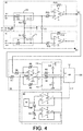
- the disclosure is not limited thereto. As illustrated in FIG. 3
- a configuration in which the negative output terminal x3 of the differential output amplifier A3 is connected to the negative input terminal n4 of the AD conversion circuit 40 via the low-pass filter F3, and the positive output terminal y3 of the differential output amplifier A3 is connected to the positive input terminal p4 of the AD conversion circuit 40 via the low-pass filter F4 in order to reduce noise in the route between the differential output amplifier A3 and the analog-to-digital conversion circuit 40 may also be employed.
- the disclosure is not limited to the aforementioned embodiments, and for example, a configuration obtained by removing the low-pass filters F2, F3, and F4 in FIG. 1 can also be employed, and a configuration obtained by removing the operational amplifiers A1 and A2 in FIG. 3 can also be employed. Configurations obtained by appropriately combining technical mechanisms disclosed in different examples are also included in the embodiments.
Landscapes
- Engineering & Computer Science (AREA)
- Theoretical Computer Science (AREA)
- Power Engineering (AREA)
- Analogue/Digital Conversion (AREA)
- Amplifiers (AREA)
- Networks Using Active Elements (AREA)
Abstract
Description
- The disclosure relates to a signal processing circuit that performs AD conversion (analog-to-digital conversion).
-
Patent Document 1 discloses a configuration using a differential amplifier for AD conversion of a differential input signal. - [Patent Document 1] Japanese Laid-open No.
2006-20171 (published on January 19, 2006 - The configuration disclosed in
Patent Document 1 has a poor noise removing effect with which it is not possible to address increasing an input range and a resolution. - According to an embodiment, a signal processing circuit includes: a first pre-stage circuit that includes a first input terminal for receiving one of differential input; a second pre-stage circuit that includes a second input terminal for receiving another one of the differential input; a post-stage circuit that includes a differential output amplifier; and an analog-to-digital conversion circuit that is connected to the post-stage circuit. The first pre-stage circuit includes a first resistive element with one end connected to the first input terminal and a first capacitative element with one grounded electrode. The other end of the first resistive element and the other electrode of the first capacitative element are connected to each other. An output node of the first pre-stage circuit and an output node of the second pre-stage circuit are connected to the post-stage circuit.
- With the aforementioned configuration, it is possible to remove high-frequency noise mixed into a signal that is input to the first input terminal since the first resistive element and the first capacitative element form a low-pass filter. Also, it is possible to remove common-mode noise of a differential input signal with the differential output amplifier. In this manner, it is possible to increase an input range and a resolution.
- The post-stage circuit may include a second resistive element with one end connected to a negative output terminal of the differential output amplifier and a second capacitative element with one grounded electrode. The other end of the second resistive element, the other electrode of the second capacitative element, and one of two input terminals of the analog-to-digital conversion circuit may be connected to each other.
- Circuit configurations of the first pre-stage circuit and the second pre-stage circuit may be the same.
- The second pre-stage circuit may include a third resistive element with one end connected to the second input terminal and a third capacitative element with one grounded electrode. The other end of the third resistive element and the other electrode of the third capacitative element may be connected to each other.
- The post-stage circuit may include a fourth resistive element with one end connected to a positive output terminal of the differential output amplifier and a fourth capacitative element with one grounded electrode. The other end of the fourth resistive element, the other electrode of the fourth capacitative element, and the other of the two input terminals of the analog-to-digital conversion circuit may be connected to each other.
- The negative output terminal and a positive input terminal of the differential output amplifier may be connected via a fifth resistive element, and the positive output terminal and a negative input terminal of the differential output amplifier may be connected via a sixth resistive element.
- Resistance values of the first resistive element and the third resistive element may be the same, resistance values of the second resistive element and the fourth resistive element may be the same, capacitance values of the first capacitative element and the third capacitative element may be the same, and capacitative values of the second capacitative element and the fourth capacitative element may be the same.
- The output node of the first pre-stage circuit may be connected to the positive input terminal of the differential output amplifier via a seventh resistive element, and the output node of the second pre-stage circuit may be connected to the negative input terminal of the differential output amplifier via an eighth resistive element.
- The first pre-stage circuit and the second pre-stage circuit may be connected to each other via a fifth capacitative element.
- Analog signals from an external device may be supplied to the first input terminal and the second input terminal.
- According to the embodiments, it is possible to increase an input range and a resolution.
-
-
FIG. 1 is a block diagram illustrating a configuration of a signal processing circuit according to an embodiment. -
FIGS. 2a to 2c are graphs illustrating operations of the signal processing circuit according to the embodiment. -
FIG. 3 is a circuit diagram illustrating a configuration of a signal processing circuit according to a first embodiment. -
FIG. 4 is a circuit diagram illustrating a configuration of a signal processing circuit according to a second embodiment. -
FIG. 1 is a block diagram illustrating a configuration of a signal processing circuit according to an embodiment.FIGS. 2a to 2c are graphs illustrating operations of the signal processing circuit according to the embodiment. - As illustrated in
FIG. 1 , asignal processing circuit 5 includes apre-stage circuit 10 that receives a positive side (S1) of the analog differential input signals S1 and S2 from an external device 6 (a sensor, for example), apre-stage circuit 20 that receives a negative side (S2) of the analog differential input signals S1 and S2, apost-stage circuit 30 that includes a differential output amplifier A3, and anAD conversion circuit 40 that is connected to thepost-stage circuit 30. - The
pre-stage circuit 10 includes a low-pass filter F1, and thepre-stage circuit 20 includes a low-pass filter F2. The input signal S1 is input to a positive input terminal of the differential output amplifier A3 via the low-pass filter F1, and the input signal S2 is input to a negative input terminal of the differential output amplifier A3 via the low-pass filter F2. - The differential output amplifier A3 is adapted to generate a negative output signal and a positive output signal using Vocm as a central voltage, and a difference between the positive output signal and the negative output signal is a value corresponding to a difference between a positive input signal and a negative input signal. The negative output signal of the differential output amplifier A3 is input to the
AD conversion circuit 40 via a low-pass filter F3, and the positive output signal of the differential output amplifier A3 is input to theAD conversion circuit 40 via a low-pass filter F4. Note that the negative output signal of the differential output amplifier A3 is fed back to the positive input terminal of the differential output amplifier A3, and the positive output signal of the differential output amplifier A3 is fed back to the negative input terminal of the differential output amplifier A3. - The
AD conversion circuit 40 performs AD conversion on a difference between the negative output signal and the positive output signal of the differential output amplifier A3, thereby generating a digital output signal DS. The digital output signal DS is input to a control unit 7 (a programmable logic controller (PLC), for example). - As illustrated in
FIG. 2a , in a case in which resolution of theAD conversion circuit 40 is assumed to be 250,000 (corresponding to 18 bits) and a range of the differential input signals S1 and S2 (input values) is assumed to be -12.5 [V] to +12.5 [V], for example, a range of the digital output signal DS (output value) is from -125,000 to +125,000. A sampling period of theAD conversion circuit 40 is assumed to be 5 [µm] to 10 [µm], for example. - A
signal processing circuit 5 converts the analog differential input signals S1 and S2 as illustrated inFIG. 2b into the digital output signal DS as illustrated inFIG. 2c . For example, S1 = +10 [V], S2 = 0 [V], and DS = 100,000 at a time t1. - As illustrated in
FIGS. 2b and 2c , the low-pass filter F1 removes high-frequency noise mixed into the input signal S1, and the low-pass filter F2 removes high-frequency noise mixed into the input signal S2. The differential output amplifier A3 removes common-mode noise in the differential input signals S1 and S2. - It is possible to remove common-mode noise (caused by the
AD conversion circuit 40 with high resolution, for example) in a route between the differential output amplifier A3 and the analog-to-digital conversion circuit 40 by using the differential output amplifier A3 (of differential outputs rather than single-end outputs). - The low-pass filter F3 removes high-frequency noise (caused by the
AD conversion circuit 40 with high resolution, for example) mixed into the negative output signal of the differential output amplifier A3, and the low-pass filter F4 removes high-frequency noise (caused by theAD conversion circuit 40 with high resolution, for example) mixed into the positive output signal of the differential output amplifier A3. - Since the negative output signal of the differential output amplifier A3 is fed back to the positive input terminal of the differential output amplifier A3, it is possible to remove noise (caused by the
AD conversion circuit 40 with high resolution, for example) in a route between the negative output terminal of the differential output amplifier A3 and the analog-to-digital conversion circuit 40. Since the positive output signal of the differential output amplifier A3 is fed back to the negative input terminal of the differential output amplifier A3, it is possible to remove noise (caused by theAD conversion circuit 40 with high resolution, for example) in a route between the positive output terminal of the differential output amplifier A3 and the analog-to-digital conversion circuit 40. - As described above, it is possible to increase an input range and a resolution since the
signal processing circuit 5 has an excellent noise removing function (noise resistance). -
FIG. 3 is a circuit diagram illustrating a configuration of a signal processing circuit according to a first embodiment. As illustrated inFIG. 3 , the signal processing circuit 5 (an analog input unit, for example) includes thepre-stage circuits post-stage circuit 30, theAD conversion circuit 40, and a referencevoltage generation circuit 50. - The
pre-stage circuit 10 includes an input terminal i1 (first input terminal) on the positive side, resistive elements R1, R11, R12, and R13, a capacitative element C1, and an operational amplifier A1. One end of the resistive element R1 is connected to the input terminal i1, one electrode of the capacitative element C1 is grounded, and the other end of the resistive element R1 and the other electrode of the capacitative element C1 are connected to each other. The resistive element R1 (first resistive element) and the capacitative element C1 (first capacitative element) form the low-pass filter F1. The other end of the resistive element R1 is grounded via the resistive element R11 and is also connected to a positive input terminal p1 of the operational amplifier A1 via the resistive element R12. A negative input terminal n1 of the operational amplifier A1 is connected to an output terminal z1 of the operational amplifier A1 via the resistive element R13. The resistive elements R12 and R13 and the operational amplifier A1 function as a buffer circuit, for example. The output terminal z1 of the operational amplifier A1 is coupled to an output node K1 of thepre-stage circuit 10. The input terminal i1 is for inputting a voltage signal, and an input terminal I1 (on the positive side) is for inputting a current signal. - The
pre-stage circuit 20 includes an input terminal i2 (second input terminal) on the negative side, resistive elements R3, R21, R22 and R23, a capacitative element C3, and an operational amplifier A2. One end of the resistive element R3 is connected to the input terminal i2, one electrode of the capacitative element C3 is grounded, and the other end of the resistive element R3 and the other electrode of the capacitative element C3 are connected to each other. The resistive element R3 (third resistive element) and the capacitative element C3 (third capacitative element) form the low-pass filter F2. The other end of the resistive element R3 is grounded via the resistive element R21 and is also connected to a positive input terminal p2 of the operational amplifier A2 via the resistive element R22. A negative input terminal n2 of the operational amplifier A2 is connected to an output terminal z2 of the operational amplifier A2 via the resistive element R23. The resistive elements R22 and R23, and the operational amplifier A2 function as a buffer circuit, for example. The output terminal z2 of the operational amplifier A2 is coupled to an output node K2 of thepre-stage circuit 20. The input terminal i2 is for inputting a voltage signal, and an input terminal I2 (on the negative side) is for inputting a current signal. The input terminal I2 is connected to the input terminal i2 via a fuse J and a resistive element. - The other end of the resistive element R3 of the
pre-stage circuit 20 is connected to the other end of the resistive element R1 of thepre-stage circuit 10 via a capacitative element C5 (fifth capacitative element). In this manner, it is possible to secure a balance of signal processing between thepre-stage circuit 10 and thepre-stage circuit 20. - The
post-stage circuit 30 includes resistive elements R2, R4, R5, R6, R7, and R8, capacitative elements C2 and C4, and the differential output amplifier A3. The output node K1 of thepre-stage circuit 10 is connected to a positive input terminal p3 of the differential output amplifier A3 via the resistive element R7 (seventh resistive element), and the output node K2 of thepre-stage circuit 20 is connected to a negative input terminal n3 of the differential output amplifier A3 via the resistive element R8 (eighth resistive element). The differential output amplifier A3 is adapted to generate a negative output signal and a positive output signal using Vocm as a central voltage, and a difference between the positive output signal and the negative output signal is a value corresponding to a difference between a positive input signal and a negative input signal. - One end of the resistive element R2 is connected to a negative output terminal x3 of the differential output amplifier A3, one electrode of the capacitative element C2 is grounded, and the other end of the resistive element R2, the other electrode of the capacitative element C2, and a positive input terminal p4 of the
AD conversion circuit 40 are connected to each other. The resistive element R2 (second resistive element) and the capacitative element C2 (second capacitative element) form the low-pass filter F3. - One end of the resistive element R4 is connected to a positive output terminal y3 of the differential output amplifier A3, one electrode of the capacitative element C4 is grounded, and the other end of the resistive element R4, the other electrode of the capacitative element C4, and a negative input terminal n4 of the
AD conversion circuit 40 are connected to each other. The resistive element R4 (fourth resistive element) and the capacitative element C4 (fourth capacitative element) form the low-pass filter F4. - The negative output terminal x3 of the differential output amplifier A3 is feedback-connected to the positive input terminal p3 of the differential output amplifier A3 via the resistive element R5, and the positive output terminal y3 of the differential output amplifier A3 is feedback-connected to the negative input terminal n3 of the differential output amplifier A3 via the resistive element R6.
- The reference
voltage generation circuit 50 includes a reference IC (integrated circuit) 60, resistive elements R30 and R31 and operational amplifiers A5 and A6 and generates the central voltage Vocm for the differential output amplifier A3 and a reference voltage Vref for theAD conversion circuit 40. - An output of the
reference IC 60 is connected to a positive input terminal p5 of the operational amplifier A5, and the reference voltage Vref that is an output of the operational amplifier A5 is input to theAD conversion circuit 40. An output terminal z5 of the operational amplifier A5 is connected to a negative input terminal n5 thereof. - An output of the
reference IC 60 is connected to a positive input terminal p6 of the operational amplifier A6 via the resistive element R30, the positive input terminal p6 is grounded via the resistive element R31, and Vocm that is an output of the operational amplifier A6 is input as a central voltage to the differential output amplifier A3. An output terminal z6 of the operational amplifier A6 is connected to a negative input terminal n6 thereof. - If it is assumed that Vocm = 1.25 [V] and Vref = 2.5 [V], the positive input signal of the differential output amplifier A3 = 1.0 [V], the negative input signal of the differential output amplifier A3 = 0 [V], and the positive output signal of the differential output amplifier A3 = 2.25 [V], and the negative output signal of the differential output amplifier A3 = 0.25 [V] at t1 (S1 = +10 [V] and S2 = 0 [V]) in
FIGS. 2b and 2c , for example. Since theAD conversion circuit 40 causes Vref = 2.5 [V] to correspond to +125,000, a digital output value becomes 100,000 at t1 at which the difference between the positive output signal and the negative output signal of the differential output amplifier A3 is 2.0 [V]. - In Example 1, the
pre-stage circuit 10 and thepre-stage circuit 20 may have the same circuit configurations, and the resistance value of the resistive element R1 = the resistance value of the resistive element R3, the capacitance value of the capacitative element C1 = the capacitance value of the capacitative element C3, the resistance value of the resistive element R11 = the resistance value of the resistive element R21, the resistance value of the resistive element R12 = the resistance value of the resistive element R22, and the resistance value of the resistive element R13 = the resistance value of the resistive element R23 may be satisfied. Also, in thepost-stage circuit 30, the resistance value of the resistive element R2 = the resistance value of the resistive element R4, the capacitance value of the capacitative element C2 = the capacitance value of the capacitative element C4, the resistance value of the resistive element R5 = the resistance value of the resistive element R6, and the resistance value of the resistive element R7 = the resistance value of the resistive element R8 may be satisfied. In this manner, operations can be performed even if the output of the external device on the negative side is connected to the input terminal i1 (+) and the output of the external device on the positive side is connected to the input terminal i2 (-). - Although the negative output terminal x3 of the differential output amplifier A3 is connected to the positive input terminal p4 of the
AD conversion circuit 40 via the low-pass filter F3 and the positive output terminal y3 of the differential output amplifier A3 is connected to the negative input terminal n4 of theAD conversion circuit 40 via the low-pass filter F4 in the first embodiment illustrated inFIG. 3 , the disclosure is not limited thereto. As illustrated inFIG. 4 , a configuration in which the negative output terminal x3 of the differential output amplifier A3 is connected to the negative input terminal n4 of theAD conversion circuit 40 via the low-pass filter F3, and the positive output terminal y3 of the differential output amplifier A3 is connected to the positive input terminal p4 of theAD conversion circuit 40 via the low-pass filter F4 in order to reduce noise in the route between the differential output amplifier A3 and the analog-to-digital conversion circuit 40 may also be employed. - The disclosure is not limited to the aforementioned embodiments, and for example, a configuration obtained by removing the low-pass filters F2, F3, and F4 in
FIG. 1 can also be employed, and a configuration obtained by removing the operational amplifiers A1 and A2 inFIG. 3 can also be employed. Configurations obtained by appropriately combining technical mechanisms disclosed in different examples are also included in the embodiments. -
- 10 pre-stage circuit
- 20 pre-stage circuit
- 30 post-stage circuit
- 40 AD conversion circuit
- A3 Differential output amplifier
- i1 Input terminal (positive side)
- i2 Input terminal (negative side)
- K1 Output node
- K2 Output node
- R1 to R8 Resistive element
- C1 to C5 Capacitative element
Claims (10)
- A signal processing circuit (5) characterized by comprising:a first pre-stage circuit (10) that includes a first input terminal (i1) for receiving one (S1) of differential input (S1, S2);a second pre-stage circuit (20) that includes a second input terminal (i2) for receiving another one (S2) of the differential input (S1, S2);a post-stage circuit (30) that includes a differential output amplifier (A3); andan analog-to-digital conversion circuit (40) connected to the post-stage circuit (30),wherein the first pre-stage circuit (10) includes a first resistive element (R1) with one end connected to the first input terminal (i1) and a first capacitative element (C1) with one grounded electrode,an other end of the first resistive element (R1) and an other electrode of the first capacitative element (C1) are connected to each other, andan output node (K1) of the first pre-stage circuit (10) and an output node (K2) of the second pre-stage circuit (20) are connected to the post-stage circuit (30).
- The signal processing circuit (5) according to claim 1, wherein
the post-stage circuit (30) includes a second resistive element (R2) with one end connected to a negative output terminal (x3) of the differential output amplifier (A3) and a second capacitative element (C2) with one grounded electrode, and
an other end of the second resistive element (R2), an other electrode of the second capacitative element (C2), and one of two input terminals (p4, n4) of the analog-to-digital conversion circuit (40) are connected to each other. - The signal processing circuit (5) according to claim 1 or 2, wherein circuit configurations of the first pre-stage circuit (10) and the second pre-stage circuit (20) are the same.
- The signal processing circuit (5) according to claim 2, wherein
the second pre-stage circuit (20) includes a third resistive element (R3) with one end connected to the second input terminal (i2) and a third capacitative element (C3) with one grounded electrode, and
an other end of the third resistive element (R3) and an other electrode of the third capacitative element (C3) are connected to each other. - The signal processing circuit (5) according to claim 4, wherein
the post-stage circuit (30) includes a fourth resistive element (R4) with one end connected to a positive output terminal (y3) of the differential output amplifier (A3) and a fourth capacitative element (C4) with one grounded electrode, and
an other end of the fourth resistive element (R4), an other electrode of the fourth capacitative element (C4), and the other of the two input terminals (p4, n4) of the analog-to-digital conversion circuit (40) are connected to each other. - The signal processing circuit (5) according to claim 5, wherein the negative output terminal (x3) and a positive input terminal (p3) of the differential output amplifier (A3) are connected via a fifth resistive element (R5), and the positive output terminal (y3) and a negative input terminal (n3) of the differential output amplifier (A3) are connected via a sixth resistive element (R6).
- The signal processing circuit (5) according to claim 6, wherein resistance values of the first resistive element (R1) and the third resistive element (R3) are the same, resistance values of the second resistive element (R2) and the fourth resistive element (R4) are the same, capacitance values of the first capacitative element (C1) and the third capacitative element (C3) are the same, and capacitance values of the second capacitative element (C2) and the fourth capacitative element (C4) are the same.
- The signal processing circuit (5) according to claim 6, wherein the output node (K1) of the first pre-stage circuit (10) is connected to the positive input terminal (p3) of the differential output amplifier (A3) via a seventh resistive element (R7), and the output node (K2) of the second pre-stage circuit (20) is connected to the negative input terminal (n3) of the differential output amplifier (A3) via an eighth resistive element (R8).
- The signal processing circuit (5) according to claim 6, wherein the first pre-stage circuit (10) and the second pre-stage circuit (20) are connected to each other via a fifth capacitative element (C5).
- The signal processing circuit (5) according to any one of claims 1 to 9, wherein analog signals from an external device (6) are supplied to the first input terminal (i1) and the second input terminal (i2).
Applications Claiming Priority (1)
| Application Number | Priority Date | Filing Date | Title |
|---|---|---|---|
| JP2018092482A JP7238269B2 (en) | 2018-05-11 | 2018-05-11 | signal processing circuit |
Publications (2)
| Publication Number | Publication Date |
|---|---|
| EP3570438A1 true EP3570438A1 (en) | 2019-11-20 |
| EP3570438B1 EP3570438B1 (en) | 2024-04-03 |
Family
ID=65766845
Family Applications (1)
| Application Number | Title | Priority Date | Filing Date |
|---|---|---|---|
| EP19162041.8A Active EP3570438B1 (en) | 2018-05-11 | 2019-03-11 | Signal processing circuit |
Country Status (4)
| Country | Link |
|---|---|
| US (1) | US10566984B2 (en) |
| EP (1) | EP3570438B1 (en) |
| JP (1) | JP7238269B2 (en) |
| CN (1) | CN110474636B (en) |
Citations (3)
| Publication number | Priority date | Publication date | Assignee | Title |
|---|---|---|---|---|
| JP2006020171A (en) | 2004-07-02 | 2006-01-19 | Fujitsu Ltd | Differential comparator, analog / digital converter, imaging device |
| EP2197109A1 (en) * | 2008-12-15 | 2010-06-16 | STMicroelectronics Srl | Integrated programmable gain amplifier circuit and system including said circuit |
| EP2317652A1 (en) * | 2008-08-19 | 2011-05-04 | Panasonic Corporation | Oversampling a/d converter |
Family Cites Families (20)
| Publication number | Priority date | Publication date | Assignee | Title |
|---|---|---|---|---|
| JPH0758870B2 (en) * | 1985-10-26 | 1995-06-21 | 日本電気株式会社 | Low feedback amplifier |
| JPH0552878A (en) * | 1991-08-29 | 1993-03-02 | Atsugi Unisia Corp | Detector |
| JPH06318138A (en) * | 1993-05-07 | 1994-11-15 | Honda Motor Co Ltd | AD converter |
| JPH1124785A (en) * | 1997-07-04 | 1999-01-29 | Hitachi Ltd | Semiconductor integrated circuit device and semiconductor memory system |
| US6480178B1 (en) * | 1997-08-05 | 2002-11-12 | Kabushiki Kaisha Toshiba | Amplifier circuit and liquid-crystal display unit using the same |
| US6437724B1 (en) * | 1999-11-05 | 2002-08-20 | Texas Instruments Incorporated | Fully differential flash A/D converter |
| JP3791767B2 (en) | 2001-03-27 | 2006-06-28 | 株式会社デンソー | Flying capacitor voltage detection circuit |
| JP4614704B2 (en) * | 2003-07-23 | 2011-01-19 | ルネサスエレクトロニクス株式会社 | Differential amplifier, data driver and display device |
| US7061419B2 (en) * | 2004-08-18 | 2006-06-13 | Matsushita Electric Industrial Co., Ltd. | A/D converter and A/D converting system |
| JP4556824B2 (en) * | 2005-09-27 | 2010-10-06 | 日本電気株式会社 | Differential amplifier, digital / analog converter, and display device |
| CN101282108B (en) * | 2007-04-03 | 2010-04-07 | 联詠科技股份有限公司 | Low differential voltage output circuit |
| JP5106186B2 (en) * | 2008-03-13 | 2012-12-26 | 三菱電機株式会社 | Driver circuit |
| JP2010002388A (en) * | 2008-06-23 | 2010-01-07 | Tdk Corp | Magnetic proportional current sensor |
| JP2010206237A (en) | 2009-02-27 | 2010-09-16 | Panasonic Corp | Amplification device and sensor module |
| JP2012044571A (en) | 2010-08-23 | 2012-03-01 | Seiko Epson Corp | Electric charge voltage conversion circuit, detection device, and electronic apparatus |
| JP5648690B2 (en) | 2010-09-15 | 2015-01-07 | ミツミ電機株式会社 | Comparator and AD converter having the same |
| JP5733027B2 (en) | 2011-05-31 | 2015-06-10 | ソニー株式会社 | AD converter and signal processing system |
| JP2014107730A (en) | 2012-11-28 | 2014-06-09 | Yamaha Corp | Signal processing device and amplifier |
| US9411987B2 (en) * | 2014-08-18 | 2016-08-09 | Qualcomm Incorporated | Low noise and low power passive sampling network for a switched-capacitor ADC with a slow reference generator |
| CN105720980B (en) * | 2014-12-17 | 2019-12-17 | 美国亚德诺半导体公司 | SAR DAC with dedicated reference capacitor for each bit capacitor |
-
2018
- 2018-05-11 JP JP2018092482A patent/JP7238269B2/en active Active
-
2019
- 2019-03-11 EP EP19162041.8A patent/EP3570438B1/en active Active
- 2019-03-12 CN CN201910182981.9A patent/CN110474636B/en active Active
- 2019-03-13 US US16/351,520 patent/US10566984B2/en active Active
Patent Citations (3)
| Publication number | Priority date | Publication date | Assignee | Title |
|---|---|---|---|---|
| JP2006020171A (en) | 2004-07-02 | 2006-01-19 | Fujitsu Ltd | Differential comparator, analog / digital converter, imaging device |
| EP2317652A1 (en) * | 2008-08-19 | 2011-05-04 | Panasonic Corporation | Oversampling a/d converter |
| EP2197109A1 (en) * | 2008-12-15 | 2010-06-16 | STMicroelectronics Srl | Integrated programmable gain amplifier circuit and system including said circuit |
Non-Patent Citations (2)
| Title |
|---|
| SALLY PETERSON: "Maximize performance when driving differential ADCs", 12 June 2003 (2003-06-12), pages 69 - 72, XP055469032, Retrieved from the Internet <URL:https://m.eet.com/media/1136807/302234.pdf> [retrieved on 20180420] * |
| YOUNG JIN KIM ET AL: "A high dynamic range data acquisition system for a solid-state electron Electric Dipole Moment experiment", ARXIV.ORG, CORNELL UNIVERSITY LIBRARY, 201 OLIN LIBRARY CORNELL UNIVERSITY ITHACA, NY 14853, 7 June 2011 (2011-06-07), XP080507782, DOI: 10.1063/1.3676163 * |
Also Published As
| Publication number | Publication date |
|---|---|
| CN110474636B (en) | 2023-06-09 |
| JP7238269B2 (en) | 2023-03-14 |
| CN110474636A (en) | 2019-11-19 |
| JP2019198046A (en) | 2019-11-14 |
| US20190348991A1 (en) | 2019-11-14 |
| US10566984B2 (en) | 2020-02-18 |
| EP3570438B1 (en) | 2024-04-03 |
Similar Documents
| Publication | Publication Date | Title |
|---|---|---|
| EP2327153B1 (en) | Auto-correction feedback loop for offset and ripple suppression in a chopper-stabilized amplifier | |
| JP5108449B2 (en) | Switched-capacitor amplifier without dependency on capacitance element variation and operation method thereof | |
| CN110249533B (en) | Signal processing device and signal processing method for Hall sensor | |
| US11967967B2 (en) | Signal shaping for compensation of metastable errors | |
| EP0415080B1 (en) | Device for converting unbalanced analog electric signals into fully-differential signals | |
| US8643526B1 (en) | Data acquisition system | |
| CN100571042C (en) | High Bandwidth Instruments Generate Differential Signals | |
| CN106464240A (en) | Improvement of phase interpolator linearity by combining current encoding and size encoding | |
| US6239733B1 (en) | Current interpolation circuit for use in an A/D converter | |
| EP3570438B1 (en) | Signal processing circuit | |
| US8456337B1 (en) | System to interface analog-to-digital converters to inputs with arbitrary common-modes | |
| CN116865695B (en) | Common mode signal suppression circuit of variable gain amplifier | |
| US20160181997A1 (en) | Signal amplifying circuit | |
| CN111654784B (en) | A method for realizing a universal circuit for direct selection and amplification of weak signals in complex signal environments | |
| CN107104675B (en) | Comparator and ΔΣ modulation circuit | |
| KR20030040013A (en) | A/d converter with high-speed input circuit | |
| EP1770866A1 (en) | High-speed analog/digital converter | |
| EP2059022A2 (en) | Image signal amplifying circuit and amplifying semiconductor integrated circuit | |
| CN114910060A (en) | Readout circuit for a sensor system and sensor system | |
| CN103716019B (en) | Sinusoidal wave generation circuit and audio shield | |
| EP3291443B1 (en) | Differential gain-stage circuit and method for multiplying a voltage | |
| JP2022151498A (en) | Isolation amplifier and abnormal state detection device | |
| CN105450567B (en) | Linear equalizer | |
| CN111446946B (en) | A Low Noise Fully Differential Switched Capacitor Filter with Single-Ended Output | |
| KR20250040344A (en) | Analog-digital converter |
Legal Events
| Date | Code | Title | Description |
|---|---|---|---|
| PUAI | Public reference made under article 153(3) epc to a published international application that has entered the european phase |
Free format text: ORIGINAL CODE: 0009012 |
|
| STAA | Information on the status of an ep patent application or granted ep patent |
Free format text: STATUS: REQUEST FOR EXAMINATION WAS MADE |
|
| 17P | Request for examination filed |
Effective date: 20190311 |
|
| AK | Designated contracting states |
Kind code of ref document: A1 Designated state(s): AL AT BE BG CH CY CZ DE DK EE ES FI FR GB GR HR HU IE IS IT LI LT LU LV MC MK MT NL NO PL PT RO RS SE SI SK SM TR |
|
| AX | Request for extension of the european patent |
Extension state: BA ME |
|
| RBV | Designated contracting states (corrected) |
Designated state(s): AL AT BE BG CH CY CZ DE DK EE ES FI FR GB GR HR HU IE IS IT LI LT LU LV MC MK MT NL NO PL PT RO RS SE SI SK SM TR |
|
| STAA | Information on the status of an ep patent application or granted ep patent |
Free format text: STATUS: EXAMINATION IS IN PROGRESS |
|
| 17Q | First examination report despatched |
Effective date: 20210618 |
|
| GRAP | Despatch of communication of intention to grant a patent |
Free format text: ORIGINAL CODE: EPIDOSNIGR1 |
|
| STAA | Information on the status of an ep patent application or granted ep patent |
Free format text: STATUS: GRANT OF PATENT IS INTENDED |
|
| INTG | Intention to grant announced |
Effective date: 20231013 |
|
| RIN1 | Information on inventor provided before grant (corrected) |
Inventor name: KIKUNAGA, YOSHITAKA |
|
| GRAS | Grant fee paid |
Free format text: ORIGINAL CODE: EPIDOSNIGR3 |
|
| GRAA | (expected) grant |
Free format text: ORIGINAL CODE: 0009210 |
|
| STAA | Information on the status of an ep patent application or granted ep patent |
Free format text: STATUS: THE PATENT HAS BEEN GRANTED |
|
| AK | Designated contracting states |
Kind code of ref document: B1 Designated state(s): AL AT BE BG CH CY CZ DE DK EE ES FI FR GB GR HR HU IE IS IT LI LT LU LV MC MK MT NL NO PL PT RO RS SE SI SK SM TR |
|
| REG | Reference to a national code |
Ref country code: GB Ref legal event code: FG4D |
|
| REG | Reference to a national code |
Ref country code: CH Ref legal event code: EP |
|
| REG | Reference to a national code |
Ref country code: IE Ref legal event code: FG4D |
|
| REG | Reference to a national code |
Ref country code: DE Ref legal event code: R096 Ref document number: 602019049296 Country of ref document: DE |
|
| REG | Reference to a national code |
Ref country code: LT Ref legal event code: MG9D |
|
| REG | Reference to a national code |
Ref country code: NL Ref legal event code: MP Effective date: 20240403 |
|
| REG | Reference to a national code |
Ref country code: AT Ref legal event code: MK05 Ref document number: 1673504 Country of ref document: AT Kind code of ref document: T Effective date: 20240403 |
|
| PG25 | Lapsed in a contracting state [announced via postgrant information from national office to epo] |
Ref country code: NL Free format text: LAPSE BECAUSE OF FAILURE TO SUBMIT A TRANSLATION OF THE DESCRIPTION OR TO PAY THE FEE WITHIN THE PRESCRIBED TIME-LIMIT Effective date: 20240403 |
|
| PG25 | Lapsed in a contracting state [announced via postgrant information from national office to epo] |
Ref country code: NL Free format text: LAPSE BECAUSE OF FAILURE TO SUBMIT A TRANSLATION OF THE DESCRIPTION OR TO PAY THE FEE WITHIN THE PRESCRIBED TIME-LIMIT Effective date: 20240403 |
|
| PG25 | Lapsed in a contracting state [announced via postgrant information from national office to epo] |
Ref country code: IS Free format text: LAPSE BECAUSE OF FAILURE TO SUBMIT A TRANSLATION OF THE DESCRIPTION OR TO PAY THE FEE WITHIN THE PRESCRIBED TIME-LIMIT Effective date: 20240803 |
|
| PG25 | Lapsed in a contracting state [announced via postgrant information from national office to epo] |
Ref country code: BG Free format text: LAPSE BECAUSE OF FAILURE TO SUBMIT A TRANSLATION OF THE DESCRIPTION OR TO PAY THE FEE WITHIN THE PRESCRIBED TIME-LIMIT Effective date: 20240403 |
|
| PG25 | Lapsed in a contracting state [announced via postgrant information from national office to epo] |
Ref country code: HR Free format text: LAPSE BECAUSE OF FAILURE TO SUBMIT A TRANSLATION OF THE DESCRIPTION OR TO PAY THE FEE WITHIN THE PRESCRIBED TIME-LIMIT Effective date: 20240403 Ref country code: FI Free format text: LAPSE BECAUSE OF FAILURE TO SUBMIT A TRANSLATION OF THE DESCRIPTION OR TO PAY THE FEE WITHIN THE PRESCRIBED TIME-LIMIT Effective date: 20240403 |
|
| PG25 | Lapsed in a contracting state [announced via postgrant information from national office to epo] |
Ref country code: GR Free format text: LAPSE BECAUSE OF FAILURE TO SUBMIT A TRANSLATION OF THE DESCRIPTION OR TO PAY THE FEE WITHIN THE PRESCRIBED TIME-LIMIT Effective date: 20240704 |
|
| PG25 | Lapsed in a contracting state [announced via postgrant information from national office to epo] |
Ref country code: PT Free format text: LAPSE BECAUSE OF FAILURE TO SUBMIT A TRANSLATION OF THE DESCRIPTION OR TO PAY THE FEE WITHIN THE PRESCRIBED TIME-LIMIT Effective date: 20240805 |
|
| PG25 | Lapsed in a contracting state [announced via postgrant information from national office to epo] |
Ref country code: ES Free format text: LAPSE BECAUSE OF FAILURE TO SUBMIT A TRANSLATION OF THE DESCRIPTION OR TO PAY THE FEE WITHIN THE PRESCRIBED TIME-LIMIT Effective date: 20240403 |
|
| PG25 | Lapsed in a contracting state [announced via postgrant information from national office to epo] |
Ref country code: CZ Free format text: LAPSE BECAUSE OF FAILURE TO SUBMIT A TRANSLATION OF THE DESCRIPTION OR TO PAY THE FEE WITHIN THE PRESCRIBED TIME-LIMIT Effective date: 20240403 |
|
| PG25 | Lapsed in a contracting state [announced via postgrant information from national office to epo] |
Ref country code: AT Free format text: LAPSE BECAUSE OF FAILURE TO SUBMIT A TRANSLATION OF THE DESCRIPTION OR TO PAY THE FEE WITHIN THE PRESCRIBED TIME-LIMIT Effective date: 20240403 |
|
| PG25 | Lapsed in a contracting state [announced via postgrant information from national office to epo] |
Ref country code: PL Free format text: LAPSE BECAUSE OF FAILURE TO SUBMIT A TRANSLATION OF THE DESCRIPTION OR TO PAY THE FEE WITHIN THE PRESCRIBED TIME-LIMIT Effective date: 20240403 |
|
| PG25 | Lapsed in a contracting state [announced via postgrant information from national office to epo] |
Ref country code: LV Free format text: LAPSE BECAUSE OF FAILURE TO SUBMIT A TRANSLATION OF THE DESCRIPTION OR TO PAY THE FEE WITHIN THE PRESCRIBED TIME-LIMIT Effective date: 20240403 |
|
| PG25 | Lapsed in a contracting state [announced via postgrant information from national office to epo] |
Ref country code: PT Free format text: LAPSE BECAUSE OF FAILURE TO SUBMIT A TRANSLATION OF THE DESCRIPTION OR TO PAY THE FEE WITHIN THE PRESCRIBED TIME-LIMIT Effective date: 20240805 Ref country code: PL Free format text: LAPSE BECAUSE OF FAILURE TO SUBMIT A TRANSLATION OF THE DESCRIPTION OR TO PAY THE FEE WITHIN THE PRESCRIBED TIME-LIMIT Effective date: 20240403 Ref country code: NO Free format text: LAPSE BECAUSE OF FAILURE TO SUBMIT A TRANSLATION OF THE DESCRIPTION OR TO PAY THE FEE WITHIN THE PRESCRIBED TIME-LIMIT Effective date: 20240703 Ref country code: LV Free format text: LAPSE BECAUSE OF FAILURE TO SUBMIT A TRANSLATION OF THE DESCRIPTION OR TO PAY THE FEE WITHIN THE PRESCRIBED TIME-LIMIT Effective date: 20240403 Ref country code: IS Free format text: LAPSE BECAUSE OF FAILURE TO SUBMIT A TRANSLATION OF THE DESCRIPTION OR TO PAY THE FEE WITHIN THE PRESCRIBED TIME-LIMIT Effective date: 20240803 Ref country code: HR Free format text: LAPSE BECAUSE OF FAILURE TO SUBMIT A TRANSLATION OF THE DESCRIPTION OR TO PAY THE FEE WITHIN THE PRESCRIBED TIME-LIMIT Effective date: 20240403 Ref country code: GR Free format text: LAPSE BECAUSE OF FAILURE TO SUBMIT A TRANSLATION OF THE DESCRIPTION OR TO PAY THE FEE WITHIN THE PRESCRIBED TIME-LIMIT Effective date: 20240704 Ref country code: FI Free format text: LAPSE BECAUSE OF FAILURE TO SUBMIT A TRANSLATION OF THE DESCRIPTION OR TO PAY THE FEE WITHIN THE PRESCRIBED TIME-LIMIT Effective date: 20240403 Ref country code: ES Free format text: LAPSE BECAUSE OF FAILURE TO SUBMIT A TRANSLATION OF THE DESCRIPTION OR TO PAY THE FEE WITHIN THE PRESCRIBED TIME-LIMIT Effective date: 20240403 Ref country code: CZ Free format text: LAPSE BECAUSE OF FAILURE TO SUBMIT A TRANSLATION OF THE DESCRIPTION OR TO PAY THE FEE WITHIN THE PRESCRIBED TIME-LIMIT Effective date: 20240403 Ref country code: BG Free format text: LAPSE BECAUSE OF FAILURE TO SUBMIT A TRANSLATION OF THE DESCRIPTION OR TO PAY THE FEE WITHIN THE PRESCRIBED TIME-LIMIT Effective date: 20240403 Ref country code: AT Free format text: LAPSE BECAUSE OF FAILURE TO SUBMIT A TRANSLATION OF THE DESCRIPTION OR TO PAY THE FEE WITHIN THE PRESCRIBED TIME-LIMIT Effective date: 20240403 Ref country code: RS Free format text: LAPSE BECAUSE OF FAILURE TO SUBMIT A TRANSLATION OF THE DESCRIPTION OR TO PAY THE FEE WITHIN THE PRESCRIBED TIME-LIMIT Effective date: 20240703 |
|
| REG | Reference to a national code |
Ref country code: DE Ref legal event code: R097 Ref document number: 602019049296 Country of ref document: DE |
|
| PG25 | Lapsed in a contracting state [announced via postgrant information from national office to epo] |
Ref country code: DK Free format text: LAPSE BECAUSE OF FAILURE TO SUBMIT A TRANSLATION OF THE DESCRIPTION OR TO PAY THE FEE WITHIN THE PRESCRIBED TIME-LIMIT Effective date: 20240403 |
|
| PG25 | Lapsed in a contracting state [announced via postgrant information from national office to epo] |
Ref country code: EE Free format text: LAPSE BECAUSE OF FAILURE TO SUBMIT A TRANSLATION OF THE DESCRIPTION OR TO PAY THE FEE WITHIN THE PRESCRIBED TIME-LIMIT Effective date: 20240403 |
|
| PG25 | Lapsed in a contracting state [announced via postgrant information from national office to epo] |
Ref country code: RO Free format text: LAPSE BECAUSE OF FAILURE TO SUBMIT A TRANSLATION OF THE DESCRIPTION OR TO PAY THE FEE WITHIN THE PRESCRIBED TIME-LIMIT Effective date: 20240403 Ref country code: SK Free format text: LAPSE BECAUSE OF FAILURE TO SUBMIT A TRANSLATION OF THE DESCRIPTION OR TO PAY THE FEE WITHIN THE PRESCRIBED TIME-LIMIT Effective date: 20240403 |
|
| PG25 | Lapsed in a contracting state [announced via postgrant information from national office to epo] |
Ref country code: SM Free format text: LAPSE BECAUSE OF FAILURE TO SUBMIT A TRANSLATION OF THE DESCRIPTION OR TO PAY THE FEE WITHIN THE PRESCRIBED TIME-LIMIT Effective date: 20240403 |
|
| PG25 | Lapsed in a contracting state [announced via postgrant information from national office to epo] |
Ref country code: SM Free format text: LAPSE BECAUSE OF FAILURE TO SUBMIT A TRANSLATION OF THE DESCRIPTION OR TO PAY THE FEE WITHIN THE PRESCRIBED TIME-LIMIT Effective date: 20240403 Ref country code: SK Free format text: LAPSE BECAUSE OF FAILURE TO SUBMIT A TRANSLATION OF THE DESCRIPTION OR TO PAY THE FEE WITHIN THE PRESCRIBED TIME-LIMIT Effective date: 20240403 Ref country code: RO Free format text: LAPSE BECAUSE OF FAILURE TO SUBMIT A TRANSLATION OF THE DESCRIPTION OR TO PAY THE FEE WITHIN THE PRESCRIBED TIME-LIMIT Effective date: 20240403 Ref country code: EE Free format text: LAPSE BECAUSE OF FAILURE TO SUBMIT A TRANSLATION OF THE DESCRIPTION OR TO PAY THE FEE WITHIN THE PRESCRIBED TIME-LIMIT Effective date: 20240403 Ref country code: DK Free format text: LAPSE BECAUSE OF FAILURE TO SUBMIT A TRANSLATION OF THE DESCRIPTION OR TO PAY THE FEE WITHIN THE PRESCRIBED TIME-LIMIT Effective date: 20240403 |
|
| PLBE | No opposition filed within time limit |
Free format text: ORIGINAL CODE: 0009261 |
|
| STAA | Information on the status of an ep patent application or granted ep patent |
Free format text: STATUS: NO OPPOSITION FILED WITHIN TIME LIMIT |
|
| 26N | No opposition filed |
Effective date: 20250106 |
|
| PGFP | Annual fee paid to national office [announced via postgrant information from national office to epo] |
Ref country code: DE Payment date: 20250327 Year of fee payment: 7 |
|
| PG25 | Lapsed in a contracting state [announced via postgrant information from national office to epo] |
Ref country code: SI Free format text: LAPSE BECAUSE OF FAILURE TO SUBMIT A TRANSLATION OF THE DESCRIPTION OR TO PAY THE FEE WITHIN THE PRESCRIBED TIME-LIMIT Effective date: 20240403 |
|
| PG25 | Lapsed in a contracting state [announced via postgrant information from national office to epo] |
Ref country code: SE Free format text: LAPSE BECAUSE OF FAILURE TO SUBMIT A TRANSLATION OF THE DESCRIPTION OR TO PAY THE FEE WITHIN THE PRESCRIBED TIME-LIMIT Effective date: 20240403 |
|
| PG25 | Lapsed in a contracting state [announced via postgrant information from national office to epo] |
Ref country code: MC Free format text: LAPSE BECAUSE OF FAILURE TO SUBMIT A TRANSLATION OF THE DESCRIPTION OR TO PAY THE FEE WITHIN THE PRESCRIBED TIME-LIMIT Effective date: 20240403 |
|
| REG | Reference to a national code |
Ref country code: CH Ref legal event code: H13 Free format text: ST27 STATUS EVENT CODE: U-0-0-H10-H13 (AS PROVIDED BY THE NATIONAL OFFICE) Effective date: 20251023 |
|
| PG25 | Lapsed in a contracting state [announced via postgrant information from national office to epo] |
Ref country code: LU Free format text: LAPSE BECAUSE OF NON-PAYMENT OF DUE FEES Effective date: 20250311 |
|
| GBPC | Gb: european patent ceased through non-payment of renewal fee |
Effective date: 20250311 |
|
| REG | Reference to a national code |
Ref country code: BE Ref legal event code: MM Effective date: 20250331 |
|
| PG25 | Lapsed in a contracting state [announced via postgrant information from national office to epo] |
Ref country code: GB Free format text: LAPSE BECAUSE OF NON-PAYMENT OF DUE FEES Effective date: 20250311 |
|
| PG25 | Lapsed in a contracting state [announced via postgrant information from national office to epo] |
Ref country code: FR Free format text: LAPSE BECAUSE OF NON-PAYMENT OF DUE FEES Effective date: 20250331 |
|
| PG25 | Lapsed in a contracting state [announced via postgrant information from national office to epo] |
Ref country code: BE Free format text: LAPSE BECAUSE OF NON-PAYMENT OF DUE FEES Effective date: 20250331 |
|
| PG25 | Lapsed in a contracting state [announced via postgrant information from national office to epo] |
Ref country code: CH Free format text: LAPSE BECAUSE OF NON-PAYMENT OF DUE FEES Effective date: 20250331 |
|
| PG25 | Lapsed in a contracting state [announced via postgrant information from national office to epo] |
Ref country code: IE Free format text: LAPSE BECAUSE OF NON-PAYMENT OF DUE FEES Effective date: 20250311 |
|
| PG25 | Lapsed in a contracting state [announced via postgrant information from national office to epo] |
Ref country code: IT Free format text: LAPSE BECAUSE OF FAILURE TO SUBMIT A TRANSLATION OF THE DESCRIPTION OR TO PAY THE FEE WITHIN THE PRESCRIBED TIME-LIMIT Effective date: 20240403 |
|
| PG25 | Lapsed in a contracting state [announced via postgrant information from national office to epo] |
Ref country code: CY Free format text: LAPSE BECAUSE OF FAILURE TO SUBMIT A TRANSLATION OF THE DESCRIPTION OR TO PAY THE FEE WITHIN THE PRESCRIBED TIME-LIMIT Effective date: 20240403 |
|
| PG25 | Lapsed in a contracting state [announced via postgrant information from national office to epo] |
Ref country code: LT Free format text: LAPSE BECAUSE OF FAILURE TO SUBMIT A TRANSLATION OF THE DESCRIPTION OR TO PAY THE FEE WITHIN THE PRESCRIBED TIME-LIMIT Effective date: 20240403 |
|
| PG25 | Lapsed in a contracting state [announced via postgrant information from national office to epo] |
Ref country code: TR Free format text: LAPSE BECAUSE OF FAILURE TO SUBMIT A TRANSLATION OF THE DESCRIPTION OR TO PAY THE FEE WITHIN THE PRESCRIBED TIME-LIMIT Effective date: 20240403 |