EP3570177B1 - Usb-schnittstellenschaltungen und mobile vorrichtungen - Google Patents
Usb-schnittstellenschaltungen und mobile vorrichtungen Download PDFInfo
- Publication number
- EP3570177B1 EP3570177B1 EP18800022.8A EP18800022A EP3570177B1 EP 3570177 B1 EP3570177 B1 EP 3570177B1 EP 18800022 A EP18800022 A EP 18800022A EP 3570177 B1 EP3570177 B1 EP 3570177B1
- Authority
- EP
- European Patent Office
- Prior art keywords
- circuit
- voltage
- output
- resistor
- biasing circuit
- Prior art date
- Legal status (The legal status is an assumption and is not a legal conclusion. Google has not performed a legal analysis and makes no representation as to the accuracy of the status listed.)
- Active
Links
Images

Classifications
-
- G—PHYSICS
- G06—COMPUTING OR CALCULATING; COUNTING
- G06F—ELECTRIC DIGITAL DATA PROCESSING
- G06F13/00—Interconnection of, or transfer of information or other signals between, memories, input/output devices or central processing units
- G06F13/38—Information transfer, e.g. on bus
- G06F13/40—Bus structure
- G06F13/4063—Device-to-bus coupling
- G06F13/4068—Electrical coupling
-
- H—ELECTRICITY
- H04—ELECTRIC COMMUNICATION TECHNIQUE
- H04M—TELEPHONIC COMMUNICATION
- H04M1/00—Substation equipment, e.g. for use by subscribers
- H04M1/72—Mobile telephones; Cordless telephones, i.e. devices for establishing wireless links to base stations without route selection
- H04M1/724—User interfaces specially adapted for cordless or mobile telephones
- H04M1/72403—User interfaces specially adapted for cordless or mobile telephones with means for local support of applications that increase the functionality
- H04M1/72409—User interfaces specially adapted for cordless or mobile telephones with means for local support of applications that increase the functionality by interfacing with external accessories
-
- G—PHYSICS
- G06—COMPUTING OR CALCULATING; COUNTING
- G06F—ELECTRIC DIGITAL DATA PROCESSING
- G06F2213/00—Indexing scheme relating to interconnection of, or transfer of information or other signals between, memories, input/output devices or central processing units
- G06F2213/0042—Universal serial bus [USB]
Definitions
- USB Universal Serial Bus
- a waterproof mobile phone is quite popular among outdoor fans due to its waterproof performance.
- An exposed interface of the previous waterproof mobile phone e.g., a USB interface
- a rubber plug to shield the interface from water.
- a user needs to remove the rubber plug before using the interface. In some cases, this can cause an inconvenience to the user.
- some waterproof mobile phones are designed without a rubber plug to shield an interface from water. In such examples, the interface is exposed.
- the mobile phone may include On-The-Go (OTG) functionality, which allows a mouse, a keyboard, a USB flash disk, or another OTG device to plug into and accessed by the mobile phone.
- OTG On-The-Go
- the mobile phone detects an OTG device using an ID contact in the USB interface.
- an ID contact on the OTG device side is grounded. This allows the mobile phone to detect the connected OTG device due to a level change from a high level to a low level if the ID contact on the mobile phone side is a high level (e.g., typically 1.8V or higher).
- This disclosure provides a USB interface circuit and a mobile device so as to avoid the exposed USB interface from being damaged, while enabling an OTG device to connect with it normally.
- a mobile device which includes a USB interface circuit including a power supply circuit having an output, a USB interface having an ID contact, a trigger detection circuit having an input, and an isolation circuit located between the power supply circuit and the ID contact.
- the isolation circuit includes a first end and a second end. The first end of the isolation circuit and the output of the power supply circuit are connected with the input of the trigger detection circuit. The second end of the isolation circuit is connected with the ID contact.
- the isolation circuit is configured to control a voltage at the ID contact below a preset voltage upon detecting an OTG device is not connected with the USB interface, wherein the preset voltage is an electrolytic voltage threshold of water.
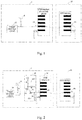
- Fig. 1 is a schematic principle diagram of a USB interface circuit 11 of a mobile phone in the related art connectable to an OTG device 12.
- an ID contact 13 of the USB interface is connected with a pull-up circuit 14 in a central processing unit (CPU) of the mobile phone so that the ID contact 13 is at a high level.
- a trigger detection circuit 15 is connected with the ID contact 13, and detects a default high-level signal.
- an ID contact 16 of the OTG device 12 is grounded so that the ID contact 13 of the USB interface is pulled from the high level down to a low level.
- the trigger detection circuit 15 detects the change in the level of the ID contact 13 from the high level to the low level, and identifies that an OTG device (e.g., the OTG device 12) is connected with the USB interface. As a result, the mobile phone can power the OTG device.
- an OTG device e.g., the OTG device 12
- a voltage at the ID contact 13 on the mobile device side remains at a high level.
- the water may be electrolyzed due to a voltage difference between the ID contact 13 and a GND contact (a ground contact) of the USB interface.
- the ID contact may be damaged (e.g., become rusted, etc.) due to the water. This damage to the ID contact may cause poor contact with other devices such as the OTG device 12. As a result, the mobile phone may not be able to identify connected devices (e.g., the OTG device 12).
- the electrolytic voltage threshold of water is 1.23V at a standard atmospheric pressure and a normal temperature of 25 degrees Celsius.
- the water will not be electrolyzed, and therefore the contact will not become rusted and possibly damaged.
- the voltage level at the ID contact on the mobile device side is maintained below the electrolytic voltage threshold of water, but the voltage at the ID contact is able to change from a high level to a low level so that an OTG device can be identified when the OTG device is connected with the USB interface.
- a USB interface circuit including a power supply circuit having an output, a USB interface having an ID contact, a trigger detection circuit having an input, and an isolation circuit located between the power supply circuit and the ID contact.
- the isolation circuit includes a first end and a second end. The first end of the isolation circuit and the output of the power supply circuit are connected with the input of the trigger detection circuit. The second end of the isolation circuit is connected with the ID contact.
- the isolation circuit is configured to control a voltage at the ID contact below a preset voltage upon detecting an OTG device is not connected with the USB interface.
- the USB interface with the ID contact may be a USB interface circuit with an ID contact.
- the isolation circuit may include a first biasing circuit having an output, a second biasing circuit having an output, and a transistor.
- the transistor includes a control end connected (e.g., electrically connected) with the output of the first biasing circuit, a first end acting as the first end of the isolation circuit, and a second end acting as the second end of the isolation circuit.
- the output of the second biasing circuit and the second end of the transistor are connected (e.g., electrically connected) with the ID contact.
- the transistor when the OTG device is not connected with the USB interface, the transistor may operate in an amplification state or a turned-off state based on a voltage at the output of the first biasing circuit and a voltage at the output of the second biasing circuit to control the voltage at the ID contact below the preset voltage.
- the transistor When the OTG device is connected with the USB interface, the transistor may operate in a saturated state to trigger the trigger detection circuit to identify the OTG device.
- Fig. 2 illustrates a schematic principle diagram of a USB interface circuit 2 according to one example embodiment of this disclosure.
- the USB interface circuit 2 includes a power supply circuit 21, a USB interface 27 with an ID contact 22, an isolation circuit 23 located between the power supply circuit 21 and the ID contact 22, and a trigger detection circuit 24.
- the isolation circuit 23 includes a first biasing circuit 232, a second biasing circuit 233, and a transistor 231.
- the transistor 231 includes a control end 2311 electrically connected with an output of the first biasing circuit 232, and first and second ends 2312, 2313.
- the first end 2312 of the transistor 231 and an output of the power supply circuit 21 are electrically connected with an input of the touch detection circuit 24.
- the second end 2313 of the transistor 231 and an output of the second biasing circuit 233 are electrically connected with the ID contact 22.
- the transistor 231 When an OTG device 25 is not connected with the USB interface 27, the transistor 231 operates in an amplification state based on a voltage at the output of the first biasing circuit 232, and a voltage at the output of the second biasing circuit 233. As a result, the power supply circuit 21 is isolated from the ID contact 22 to prevent the voltage output by the power supply circuit 21 from being fully applied to the ID contact 22, thereby controlling the voltage at the ID contact 22 below a preset voltage. However, when the OTG device 25 is connected with the USB interface 27 (as shown in Fig. 2 ), the transistor 231 operates in a saturated state to trigger the touch detection circuit 24 to identify the OTG device 25.
- the preset voltage is the electrolytic voltage threshold of water (e.g., 1.23V).
- the transistor 231 in the isolation circuit 23 may be an NPN-type Bipolar Junction Transistor (BJT) by way of an example.
- the transistor 231 may alternatively be a PNP-type BJT, although the embodiments of this disclosure are not limited thereto.
- the USB interface circuit may be located on any known device including but not limited to a mobile phone, a computer, a tablet computer, a media player, a Personal Digital Assistant (PDA), an on-vehicle device, a wearable device, a Virtual Reality (VR) on-head display device, etc., or any combination thereof.
- PDA Personal Digital Assistant
- the USB interface according to this embodiment may be applicable to a waterproof device.
- the type of the USB interface may include USB Type-A, USB Type-B, and USB-micro.
- the power supply circuit 21 includes a first power supply VI, and a first resistor R1 with one end electrically connected with the first power supply VI, and another end serving as the output of the power supply circuit 21.
- the power supply circuit 21 provides a default high level (e.g., 1.8V) as an input signal to the trigger detection circuit 24.
- the voltage of the first power supply V1 may be selected as 1.8V
- the resistance of the first resistor R1 is 10K ⁇ .
- the voltage of the first power supply VI, and the resistance of the first resistor R1 may alternatively be other values, although the embodiments of this disclosure are not limited thereto.
- the trigger detection circuit 24 includes an input end, which is configured to output a control signal for identifying the OTG device 25, according to a change of the input signal from a high level to a low level.
- Specific components of the trigger detection circuit 24 may be known to those skilled in the art, so a detailed description thereof is omitted in the embodiments of this disclosure.
- the power supply circuit 21 and the trigger detection circuit 24 may be integrated in a CPU of a device (e.g., a mobile phone), or the power supply circuit 21 and/or the trigger detection circuit 24 may arranged separate from the CPU.
- the ID contact 22 may be a conductive contact of the USB interface 27, and configured to be electrically connected with a corresponding conductive contact of the OTG device 25 when the OTG device is connected with the USB interface 27.
- the first biasing circuit 232 may provide the control end 2311 of the transistor 231 with a bias voltage, and includes a second power supply V2, and second and third resistors R2, R3.
- the second and third resistors R2, R3 are connected in series between the second power supply V2 and ground.
- the first biasing circuit 232 is a voltage divider biasing circuit with a voltage output serving as a common end of the second resistor and the third resistor.
- the output of the first biasing circuit 232 is located at an intermediate node between the second resistor R2 and the third resistor R3.
- an end of the second resistor R2 connected with the third resistor R3 acts as the output of the first biasing circuit 232
- an end of the third resistor R3 connected with the second resistor R2 acts as the output of the first biasing circuit 232.
- the second power supply V2 may have similar or different structure with that of the first power supply VI, although the embodiments of this disclosure are not limited thereto. In some embodiments of this disclosure, the voltage of the second power supply V2 may be set at the same level as the first power supply V1 (e.g., 1.8V).
- the voltage output of the first biasing circuit 232 is electrically connected with the control end 2311 of the transistor 231, and configured to apply voltage on the third resistor R3 as a result of voltage division to the control end 2311 of the transistor 231.
- the particular voltage as a result of voltage division is determined by the resistances of the second resistor R2 and the third resistor R3.
- the resistance of the second resistor R2 is 100K ⁇
- the resistance of the third resistor R3 is 150 K ⁇ , so the voltage on the third resistor R3 as a result of voltage division is 1.08V
- the second biasing circuit 233 is configured to provide the second end 2313 of the transistor 231 with a bias voltage, and in some embodiments of this disclosure, the second biasing circuit 233 includes a fourth resistor R4 (as shown in Fig. 2 ) with one end serving as the output of the second biasing circuit 233, and the other end grounded. As such, the second biasing circuit 233 may clamp the second end 2313 of the transistor 231 at a low level by default. For example, in some embodiments, the resistance of the second resistor R2 is 100K ⁇ .
- the transistor 231 is an NPN-type BJT (as illustrated in Fig. 2 ) with an amplification factor of 230.
- the control end 2311 of the transistor is a base of the BJT
- the first end 2312 of the transistor is a collector of the BJT
- the second end 2313 of the transistor is an emitter of the BJT.
- the isolation circuit 23 and the power supply circuit 21 may form a co-emitter amplification circuit.
- USB interface circuit 2 An operating principle of the USB interface circuit 2 according to this embodiment is described below when, for example, the transistor 231 is an NPN-type BJT.
- the BJT is turned on, and the BJT operates in an amplification state due to a limiting gain of current amplification.
- U b is the voltage at the base
- R e is the resistance of the emitter (e.g., the fourth resistor R4 in this embodiment)
- U be is 0.6V after the BJT is operating in the amplification state.
- the voltage at the ID contact 22 is far below the electrolytic voltage threshold (e.g., 1.23V)_ of water, so even if the USB interface 27 comes into contact with water, it will not be electrolyzed, and thus the ID contact 22 will not become rusted due to the water.
- I e I b + I c
- I c ⁇ ⁇ I b
- I b the current at the base
- I c the current at the collector
- the input signal to the trigger detection circuit 24 is maintained at the default high level (e.g., approximately 1.8V), and the trigger detection circuit 24 does not detect any change of the level from a high level to a low level, so no OTG device is identified as connected.
- the default high level e.g., approximately 1.8V
- the ID contact 26 of the OTG device is grounded directly, and the ground impedance is lower than 10 ohms.
- the fourth resistor R4 connected with the emitter of the BJT is equivalently connected in parallel with a resistor (e.g., the ground impedance) of lower than 10 ohms.
- a resistor e.g., the ground impedance
- the collector is connected directly with the emitter.
- the trigger detection circuit 24 is also equivalently grounded, so that the trigger detection circuit 24 can identify the change in the voltage from a high level to a low level, and thus the OTG device may be identified.
- the BJT isolates the trigger detection circuit 24 from the ID contact 22, resulting in different voltages for the two signals which would otherwise have been connected together.
- the voltage applied to the control end 2311 of the BJT is set reasonably, and the amplification coefficient of the BJT, and the resistance of the fourth resistor R4 are selected reasonably, so that the voltage at the second end of the transistor can be below the electrolytic voltage threshold of water, and the trigger detection circuit 24 does not detect any level change, and thus will not trigger identification of the OTG device 25.
- the ground resistor on the ID contact can be bypassed to thereby change the structure of the circuit, so that the trigger detection circuit 24 and the ID contact 22 can be reconnected, and the trigger detection circuit 24 can detect the change in the voltage on the ID contact 22, thus identifying the OTG device 25.
- the voltage of the second power supply V2 is 1.8V, for example, but may alternatively be another value if there is another appropriate power supply, as long as the resistances of the second resistor R2 and the third resistor R3 are adjusted such that the voltage divider circuit outputs a voltage as required for the voltage at the base of the BJT.
- the BJT may have a large amplification coefficient, and the resistance of the fourth resistor R4 may be far greater than that of the first resistor R1.
- the transistor 231 in the isolation circuit 23 may be a PNP-type BJT, and the first biasing circuit 232 and the second biasing circuit 233 may be set based on the operating principle of the PNP-type BJT.
- the PNP-type BJT upon detecting that the OTG device 25 is not connected with the USB interface 27, the PNP-type BJT operates in a specific state based on the voltage output by the first biasing circuit 232, and the voltage output by the second biasing circuit 233 to control the voltage at the ID contact 22 below the preset voltage, and upon detecting that the OTG device 25 is connected with the USB interface 27, the PNP-type BJT operates in another specific state to trigger the detection circuit 24 to identify the OTG device, although a detailed description thereof is omitted in the embodiment of this disclosure.
- Fig. 3 illustrates a schematic principle diagram of a USB interface circuit 2 according to another example embodiment of this disclosure.
- the USB interface circuit 2 of Fig. 3 is different from the USB interface circuit 2 of Fig. 2 in the structure of the isolation circuit 23.
- the transistor in the isolation circuit 23 in the USB interface circuit 2 of Fig. 3 is a Metal Oxide Semiconductor Field Effect Transistor (MOSFET) 331.
- the MOSFET 331 includes a control end 3311 as the gate of the MOSFET, a first end 3312 as the drain of the MOSFET, and a second end 3313 as the source of the MOSFET.
- the MOSFET 331 is an N-channel MOSFET (NMOSFET), for example.
- NMOSFET N-channel MOSFET
- the isolation circuit 23 includes a second biasing circuit 333 that is different from Fig. 2 .
- the second biasing circuit 333 includes a third power supply V3, and fifth and sixth resistors R5, R6.
- the fifth and sixth resistors R5, R6 are connected in series between the third power supply V3 and ground.
- the output of the second biasing circuit 333 serves as a common end of the fifth resistor R5 and the sixth resistor R6 (e.g., the output of the second biasing circuit 333 is located at an intermediate node between the fifth resistor R5 and the sixth resistor R6).
- an end of the fifth resistor R5 connected with the sixth resistor R6 acts as the output of the second biasing circuit 333, and/or an end of the fifth resistor R5 connected with the sixth resistor R6 acts as the output of the second biasing circuit 333.
- R5 100K ⁇
- R6 50KQ
- the voltage output by the first biasing circuit 232 of Fig. 3 is 1.1V, and the voltage output by the second biasing circuit 333 of Fig. 3 is 0.6V.
- the NMOSFET is turned off.
- the voltage at the ID contact 22 is 0.6V, which is below the electrolytic voltage threshold of water. As such, the ID contact 22 will not become rusted from water contact.
- the input signal to the trigger detection circuit 24 of Fig. 3 is maintained at a high level.
- the source of the NMOSFET 331 is grounded, and the voltage at the source is 0V.
- Vgs 1.1 which is greater than the threshold voltage of the NMOSFET 331.
- the NMOSFET is turned on in a saturated state, and the input signal to the trigger detection circuit 24 of Fig. 3 is changed from the high level to the low level thereby allowing the trigger detection circuit 24 to identify the connected OTG device.
- the corresponding function can be performed as long as the threshold voltage of the NMOSFET is greater than 0.5V and less than1.1V.
- the NMOSFET 331 in the isolation circuit 23 operates respectively in the turned-off state, and the saturated state based on the output voltage of the first biasing circuit 232, and the output voltage of the second biasing circuit 333.
- the isolation circuit 23 isolates the power supply circuit 21 from the ID contact 22 to prevent the high level of the power supply circuit 21 from being completely applied to the ID contact 22.
- the second biasing circuit 333 provides the ID contact 22 with a lower voltage so that the voltage at the ID contact 22 is below the electrolytic voltage threshold of water. Also, the input signal to the trigger detection circuit 24 is maintained at the default high level.
- the trigger detection circuit 24 When the NMOSFET 331 is operating in the saturated state, the trigger detection circuit 24 is electrically connected with the ID contact 22 so that the input signal is changed from the high level to the low level, thereby allowing the trigger detection circuit 24 to detect whether the OTG device is connected.
- the transistor 331 in the isolation circuit 23 of Fig. 3 is an N-channel MOSFET, for example.
- the transistor 331 may be a P-channel MOSFET (PMOSFET), and the first biasing circuit 232 and the second biasing circuit 333 may be configured according to the operating principle of the P-channel MOSFET.
- PMOSFET P-channel MOSFET
- the PMOSFET when the OTG device 25 is not connected with the USB interface 27, the PMOSFET operates in a specific state based on the voltage output by the first biasing circuit 232, and the voltage output by the second biasing circuit 333 to control the voltage at the ID contact 22 below the preset voltage, and when the OTG device 25 is connected with the USB interface 27, the PMOSFET operates in another specific state to trigger the detection circuit 24 to identify the OTG device 25, although a detailed description thereof is omitted in the embodiment of this disclosure.
- the isolation circuit is arranged between the power supply circuit and the ID contact of the USB interface.
- the transistor in the isolation circuit operates in the amplification or turned-off state based on the voltage output by the first biasing circuit and the voltage output by the second biasing circuit. Because the amplification and turned-off states are partially turned-on states, the isolation circuit can prevent the voltage output by the power supply circuit from being completely applied to the ID contact. Parameters of the circuit may be selected appropriately such that the voltage at the ID contact is below the electrolytic voltage threshold of water. As such, water contacting the ID contact will not be electrolyzed, and the ID contact will not become rusted due to the water.
- the voltage at the first end of the transistor is the same as the output voltage of the power supply circuit. Therefore, the trigger detection circuit will not detect any voltage level change, and thus will not identify the OTG device.
- the ID contact is equivalently grounded, the transistor operates in the saturated state, and the first end and the second end of the transistor are equivalently electrically connected directly and grounded. Because the input of the trigger detection circuit is electrically connected with the first end of the transistor, the trigger detection circuit detects the change in the voltage level from a high level to a low level, and thus identifies the OTG device.
- Embodiments of this disclosure further provide a mobile device including a USB interface circuit.
- the USB interface circuit includes a power supply circuit having an output, a USB interface having an ID contact, a trigger detection circuit having an input, and an isolation circuit located between the power supply circuit and the ID contact.
- the isolation circuit includes a first end and a second end. The first end of the isolation circuit and the output of the power supply circuit are connected with the input of the trigger detection circuit. The second end of the isolation circuit is connected with the ID contact.
- the isolation circuit is configured to control a voltage at the ID contact to below a preset voltage upon detecting that an OTG device is not connected with the USB interface.
Landscapes
- Engineering & Computer Science (AREA)
- General Engineering & Computer Science (AREA)
- Theoretical Computer Science (AREA)
- Computer Hardware Design (AREA)
- Physics & Mathematics (AREA)
- General Physics & Mathematics (AREA)
- Human Computer Interaction (AREA)
- Computer Networks & Wireless Communication (AREA)
- Signal Processing (AREA)
- Power Sources (AREA)
Claims (13)
- Mobile Einrichtung, umfassend eine USB-Schnittstellenschaltung, wobei die USB-Schnittstellenschaltung eine Energieversorgungsschaltung (21), aufweisend einen Ausgang, eine USB-Schnittstelle (27), aufweisend einen ID-Kontakt (22), eine Auslösererfassungsschaltung (24), aufweisend einen Eingang, und eine Isolationsschaltung (23), die zwischen der Energieversorgungsschaltung (21) und dem ID-Kontakt (22) angeordnet ist und ein erstes Ende und ein zweites Ende aufweist, umfasst, wobei das erste Ende der Isolationsschaltung (23) und der Ausgang der Energieversorgungsschaltung (21) mit dem Eingang der Auslösererfassungsschaltung (24) verbunden sind, das zweite Ende der Isolationsschaltung (23) mit dem ID-Kontakt (22) verbunden ist, und die Isolationsschaltung (23) eingerichtet ist, eine Spannung an dem ID-Kontakt unter eine voreingestellte Spannung zu steuern, auf Erfassen, dass eine On-The-Go-(OTG)-Einrichtung mit der USB-Schnittstelle (27) nicht verbunden ist;
wobei die voreingestellte Spannung ein elektrolytischer Spannungsschwellenwert von Wasser ist. - Mobile Einrichtung nach Anspruch 1, wobei die Isolationsschaltung (23) eine erste Vorspannungsschaltung (232), aufweisend einen Ausgang, eine zweite Vorspannungsschaltung (233, 333), aufweisend einen Ausgang, und einen Transistor (231, 331), umfasst, wobei der Transistor (231, 331) ein Steuerende (2311, 3311), das mit dem Ausgang der ersten Vorspannungsschaltung (232) verbunden ist, ein erstes Ende (2312, 3312), das als das erste Ende der Isolationsschaltung (23) wirkt, und ein zweites Ende (2313, 3313), das als das zweite Ende der Isolationsschaltung (23) wirkt, umfasst, und wobei der Ausgang der zweiten Vorspannungsschaltung (233, 333) und das zweite Ende des Transistors (231, 331) mit dem ID-Kontakt verbunden sind.
- Mobile Einrichtung nach Anspruch 2, wobei der Transistor (231) eingerichtet ist: auf Erfassen, dass die OTG-Einrichtung mit der USB-Schnittstelle (27) nicht verbunden ist,in einem Verstärkungszustand oder einem ausgeschalteten Zustand zu arbeiten auf Grundlage einer Spannung am Ausgang der ersten Vorspannungsschaltung (232) und einer Spannung am Ausgang der zweiten Vorspannungsschaltung (233), um die Spannung an dem ID-Kontakt (22) unter die voreingestellte Spannung zu steuern; undauf Erfassen, dass die OTG-Einrichtung mit der USB-Schnittstelle (27) verbunden ist, in einem gesättigten Zustand zu arbeiten, um die Auslösererfassungsschaltung (24) auszulösen und die OTG-Einrichtung zu identifizieren.
- Mobile Einrichtung nach Anspruch 2 oder 3, wobei der Transistor (231) ein Bipolar-Sperrschicht-Transistor (Bipolar Junction Transistor, BJT) ist, und wobei das Steuerende (2311) des Transistors (231) eine Basis des BJT ist, das erste Ende (2312) des Transistors ein Kollektor des BJT ist und das zweite Ende (2313) ein Emitter des BJT ist.
- Mobile Einrichtung nach Anspruch 4, wobei der BJT ein BJT vom NPN-Typ ist.
- Mobile Einrichtung nach Anspruch 5, wobei die zweite Vorspannungsschaltung (233) einen Widerstand (R4) umfasst, der ein als der Ausgang der zweiten Vorspannungsschaltung wirkendes Ende und ein anderes geerdetes Ende aufweist.
- Mobile Einrichtung nach Anspruch 6, wobei die Energieversorgungsschaltung (21) eine Energieversorgung (V1) und einen Widerstand (R1), aufweisend ein Ende, das mit der Energieversorgung (V1) verbunden ist, und ein anderes Ende, das als der Ausgang der Energieversorgungsschaltung (21) wirkt, umfasst.
- Mobile Einrichtung nach Anspruch 7, wobei der Widerstand (R4) der zweiten Vorspannungsschaltung (233) einen Widerstandswert aufweist, der das Zehnfache oder mehr des Widerstandswerts des Widerstands (R1) der Energieversorgungsschaltung (21) beträgt.
- Mobile Einrichtung nach Anspruch 5, wobei die erste Vorspannungsschaltung (232 eingerichtet ist:
auf Erfassen, dass die OTG-Einrichtung mit der USB-Schnittstelle (27) nicht verbunden ist, zu bewirken, dass eine Differenz zwischen einer Spannung am Ausgang der ersten Vorspannungsschaltung (232) und einer Spannung am Ausgang der zweiten Vorspannungsschaltung (233) über eine Schwellenspannung des BJT vom NPN-Typs ansteigt. - Mobile Einrichtung nach Anspruch 9, wobei der BJT vom NPN-Typ eingerichtet ist: auf Erfassen, dass die OTG-Einrichtung mit der USB-Schnittstelle (27) nicht verbunden ist,
in einem Verstärkungszustand zu arbeiten auf Grundlage der Spannung am Ausgang der ersten Vorspannungsschaltung (232) und der Spannung am Ausgang der zweiten Vorspannungsschaltung (233), um die Spannung am ID-Kontakt (22) unter die voreingestellte Spannung zu steuern. - Mobile Einrichtung nach Anspruch 2, wobei die erste Vorspannungsschaltung (232) eine Energieversorgung (V2), einen ersten Widerstand (R2) und einen zweiten Widerstand (R3) umfasst, wobei der erste Widerstand (R2) und der zweite Widerstand (R3) zwischen der Energieversorgung (V2) und Masse in Reihe verbunden sind, und wobei ein Ende des ersten Widerstands (R2) mit dem zweiten Widerstand verbunden ist und als der Ausgang der ersten Vorspannungsschaltung wirkt.
- Mobile Einrichtung nach Anspruch 2, wobei der Transistor (331) ein Metalloxid-Halbleiter-Feldeffekttransistor, MOSFET, ist und wobei das Steuerende (3311) des Transistors (331) ein Gate des MOSFET ist, das erste Ende (3312) des Transistors (331) ein Drain des MOSFET ist und das zweite Ende (3313) des Transistors (331) eine Source des MOSFET ist.
- Mobile Einrichtung nach Anspruch 12, wobei der MOSFET ein N-Kanal-MOSFET ist und die zweite Vorspannungsschaltung (333) eine Energieversorgung (V3), einen ersten Widerstand (R5) und einen zweiten Widerstand (R6) umfasst, wobei der erste Widerstand (R5) und der zweite Widerstand (R6) zwischen der Energieversorgung (V3) und Masse in Reihe verbunden sind, und wobei ein Ende des ersten Widerstands (R5) mit dem zweiten Widerstand (R6) verbunden ist und als der Ausgang der zweiten Vorspannungsschaltung (333) wirkt;oder,wobei der MOSFET ein N-Kanal-MOSFET ist, wobei die erste Vorspannungsschaltung eingerichtet ist: auf Erfassen, dass die OTG-Einrichtung mit der USB-Schnittstelle nicht verbunden ist, zu bewirken, dass eine Differenz zwischen einer Spannung am Ausgang der ersten Vorspannungsschaltung (232) und einer Spannung am Ausgang der zweiten Vorspannungsschaltung (333) über eine Schwellenspannung des N-Kanal-MOSFET ansteigt; und der N-Kanal-MOSFET eingerichtet ist: auf Erfassen, dass die OTG-Einrichtung mit der USB-Schnittstelle nicht verbunden ist, in einem ausgeschalteten Zustand zu arbeiten auf Grundlage der Spannung am Ausgang der ersten Vorspannungsschaltung und der Spannung am Ausgang der zweiten Vorspannungsschaltung, um die Spannung am ID-Kontakt unter die voreingestellte Spannung zu steuern.
Applications Claiming Priority (2)
| Application Number | Priority Date | Filing Date | Title |
|---|---|---|---|
| CN201810233692.2A CN108399142B (zh) | 2018-03-20 | 2018-03-20 | 一种usb接口电路及移动终端 |
| PCT/CN2018/114397 WO2019179129A1 (zh) | 2018-03-20 | 2018-11-07 | 一种usb接口电路及移动设备 |
Publications (3)
| Publication Number | Publication Date |
|---|---|
| EP3570177A1 EP3570177A1 (de) | 2019-11-20 |
| EP3570177A4 EP3570177A4 (de) | 2019-11-20 |
| EP3570177B1 true EP3570177B1 (de) | 2020-12-30 |
Family
ID=63092698
Family Applications (1)
| Application Number | Title | Priority Date | Filing Date |
|---|---|---|---|
| EP18800022.8A Active EP3570177B1 (de) | 2018-03-20 | 2018-11-07 | Usb-schnittstellenschaltungen und mobile vorrichtungen |
Country Status (3)
| Country | Link |
|---|---|
| EP (1) | EP3570177B1 (de) |
| CN (1) | CN108399142B (de) |
| WO (1) | WO2019179129A1 (de) |
Families Citing this family (3)
| Publication number | Priority date | Publication date | Assignee | Title |
|---|---|---|---|---|
| CN108399142B (zh) * | 2018-03-20 | 2021-06-01 | 青岛海信移动通信技术股份有限公司 | 一种usb接口电路及移动终端 |
| CN110932712B (zh) * | 2018-09-19 | 2023-05-05 | 青岛海信移动通信技术有限公司 | 连接器的接口电路及电子装置 |
| CN117439236B (zh) * | 2023-12-18 | 2024-03-29 | 深圳市卓芯微科技有限公司 | 一种美容仪充电触点的隔离电路、方法及美容仪 |
Family Cites Families (10)
| Publication number | Priority date | Publication date | Assignee | Title |
|---|---|---|---|---|
| CN104272216A (zh) * | 2012-05-11 | 2015-01-07 | 富士通株式会社 | 电子设备及其控制方法 |
| JP2015037269A (ja) * | 2013-08-14 | 2015-02-23 | 富士通株式会社 | 電子機器、電圧監視方法及び電圧監視プログラム |
| CN103872530B (zh) * | 2014-03-06 | 2017-03-29 | 华勤通讯技术有限公司 | Usb母座、终端设备及usb连接器 |
| KR102348784B1 (ko) * | 2015-06-26 | 2022-01-07 | 삼성전자주식회사 | 모드에 따라 신호 세기를 제어하는 전자 장치 및 방법 |
| CN104951034B (zh) * | 2015-07-16 | 2017-08-18 | 广东欧珀移动通信有限公司 | 移动终端及其usb接口状态控制方法和装置 |
| CN205721762U (zh) * | 2016-03-31 | 2016-11-23 | 维沃移动通信有限公司 | 通用串行总线usb接口的接口电路及便携式终端 |
| CN106647539A (zh) * | 2017-02-14 | 2017-05-10 | 青岛海信移动通信技术股份有限公司 | 具有防水电路的电子设备 |
| CN107300965A (zh) * | 2017-05-12 | 2017-10-27 | 青岛海信移动通信技术股份有限公司 | 一种usb接口防水的实现方法和装置 |
| CN107632949B (zh) * | 2017-09-30 | 2019-10-25 | Oppo广东移动通信有限公司 | 数据线识别电路、方法和终端 |
| CN108399142B (zh) * | 2018-03-20 | 2021-06-01 | 青岛海信移动通信技术股份有限公司 | 一种usb接口电路及移动终端 |
-
2018
- 2018-03-20 CN CN201810233692.2A patent/CN108399142B/zh active Active
- 2018-11-07 EP EP18800022.8A patent/EP3570177B1/de active Active
- 2018-11-07 WO PCT/CN2018/114397 patent/WO2019179129A1/zh not_active Ceased
Non-Patent Citations (1)
| Title |
|---|
| None * |
Also Published As
| Publication number | Publication date |
|---|---|
| CN108399142A (zh) | 2018-08-14 |
| EP3570177A1 (de) | 2019-11-20 |
| EP3570177A4 (de) | 2019-11-20 |
| CN108399142B (zh) | 2021-06-01 |
| WO2019179129A1 (zh) | 2019-09-26 |
Similar Documents
| Publication | Publication Date | Title |
|---|---|---|
| CN107852012B (zh) | 反向电流保护电路 | |
| US5382841A (en) | Switchable active bus termination circuit | |
| US8531851B2 (en) | Start-up circuit and method thereof | |
| TW475312B (en) | Apparatus and method for controlling power supply to a battery-powered electronic device | |
| US8458375B2 (en) | Portable electronic device having multifunctional audio port | |
| CN107390768B (zh) | 电子设备电力保护电路 | |
| CN205721762U (zh) | 通用串行总线usb接口的接口电路及便携式终端 | |
| JP2021522766A5 (de) | ||
| EP3570177A1 (de) | Usb-schnittstellenschaltungen und mobile vorrichtungen | |
| US10289477B2 (en) | USB electronic marker circuit and method therefor | |
| CN101373388A (zh) | 调整装置 | |
| TWI812013B (zh) | 應用於USB Type-C通訊埠之過電壓保護電路和相關過電壓保護方法 | |
| CN110932712A (zh) | 连接器的接口电路及电子装置 | |
| TW201611486A (zh) | 用於電子裝置之保護裝置及方法 | |
| US20240402778A1 (en) | Usb power delivery interface | |
| US20130313914A1 (en) | Control circuit for universal serial bus connector | |
| CN109167420B (zh) | 一种充电控制电路、充电电路及充电控制方法 | |
| US8476960B1 (en) | Identifying circuit | |
| US8520350B2 (en) | Protection circuit for digital integrated chip | |
| US7286005B2 (en) | Supply voltage switching circuit | |
| US8325052B2 (en) | Over-current protection apparatus | |
| US9627901B2 (en) | Charging circuit | |
| US20120267958A1 (en) | Current suppression circuit and electronic device employing the same | |
| US10027107B2 (en) | Electronic device with reverse voltage protection circuitry for multiple control lines | |
| CN111490570A (zh) | 保护电路及电子设备 |
Legal Events
| Date | Code | Title | Description |
|---|---|---|---|
| STAA | Information on the status of an ep patent application or granted ep patent |
Free format text: STATUS: UNKNOWN |
|
| STAA | Information on the status of an ep patent application or granted ep patent |
Free format text: STATUS: THE INTERNATIONAL PUBLICATION HAS BEEN MADE |
|
| PUAI | Public reference made under article 153(3) epc to a published international application that has entered the european phase |
Free format text: ORIGINAL CODE: 0009012 |
|
| STAA | Information on the status of an ep patent application or granted ep patent |
Free format text: STATUS: REQUEST FOR EXAMINATION WAS MADE |
|
| 17P | Request for examination filed |
Effective date: 20181121 |
|
| A4 | Supplementary search report drawn up and despatched |
Effective date: 20190910 |
|
| AK | Designated contracting states |
Kind code of ref document: A1 Designated state(s): AL AT BE BG CH CY CZ DE DK EE ES FI FR GB GR HR HU IE IS IT LI LT LU LV MC MK MT NL NO PL PT RO RS SE SI SK SM TR |
|
| AX | Request for extension of the european patent |
Extension state: BA ME |
|
| GRAP | Despatch of communication of intention to grant a patent |
Free format text: ORIGINAL CODE: EPIDOSNIGR1 |
|
| STAA | Information on the status of an ep patent application or granted ep patent |
Free format text: STATUS: GRANT OF PATENT IS INTENDED |
|
| INTG | Intention to grant announced |
Effective date: 20200630 |
|
| GRAS | Grant fee paid |
Free format text: ORIGINAL CODE: EPIDOSNIGR3 |
|
| GRAA | (expected) grant |
Free format text: ORIGINAL CODE: 0009210 |
|
| STAA | Information on the status of an ep patent application or granted ep patent |
Free format text: STATUS: THE PATENT HAS BEEN GRANTED |
|
| AK | Designated contracting states |
Kind code of ref document: B1 Designated state(s): AL AT BE BG CH CY CZ DE DK EE ES FI FR GB GR HR HU IE IS IT LI LT LU LV MC MK MT NL NO PL PT RO RS SE SI SK SM TR |
|
| DAV | Request for validation of the european patent (deleted) | ||
| DAX | Request for extension of the european patent (deleted) | ||
| REG | Reference to a national code |
Ref country code: GB Ref legal event code: FG4D |
|
| REG | Reference to a national code |
Ref country code: AT Ref legal event code: REF Ref document number: 1350629 Country of ref document: AT Kind code of ref document: T Effective date: 20210115 |
|
| REG | Reference to a national code |
Ref country code: DE Ref legal event code: R096 Ref document number: 602018011417 Country of ref document: DE |
|
| REG | Reference to a national code |
Ref country code: IE Ref legal event code: FG4D |
|
| PG25 | Lapsed in a contracting state [announced via postgrant information from national office to epo] |
Ref country code: FI Free format text: LAPSE BECAUSE OF FAILURE TO SUBMIT A TRANSLATION OF THE DESCRIPTION OR TO PAY THE FEE WITHIN THE PRESCRIBED TIME-LIMIT Effective date: 20201230 Ref country code: RS Free format text: LAPSE BECAUSE OF FAILURE TO SUBMIT A TRANSLATION OF THE DESCRIPTION OR TO PAY THE FEE WITHIN THE PRESCRIBED TIME-LIMIT Effective date: 20201230 Ref country code: GR Free format text: LAPSE BECAUSE OF FAILURE TO SUBMIT A TRANSLATION OF THE DESCRIPTION OR TO PAY THE FEE WITHIN THE PRESCRIBED TIME-LIMIT Effective date: 20210331 Ref country code: NO Free format text: LAPSE BECAUSE OF FAILURE TO SUBMIT A TRANSLATION OF THE DESCRIPTION OR TO PAY THE FEE WITHIN THE PRESCRIBED TIME-LIMIT Effective date: 20210330 |
|
| REG | Reference to a national code |
Ref country code: AT Ref legal event code: MK05 Ref document number: 1350629 Country of ref document: AT Kind code of ref document: T Effective date: 20201230 |
|
| PG25 | Lapsed in a contracting state [announced via postgrant information from national office to epo] |
Ref country code: BG Free format text: LAPSE BECAUSE OF FAILURE TO SUBMIT A TRANSLATION OF THE DESCRIPTION OR TO PAY THE FEE WITHIN THE PRESCRIBED TIME-LIMIT Effective date: 20210330 Ref country code: SE Free format text: LAPSE BECAUSE OF FAILURE TO SUBMIT A TRANSLATION OF THE DESCRIPTION OR TO PAY THE FEE WITHIN THE PRESCRIBED TIME-LIMIT Effective date: 20201230 Ref country code: LV Free format text: LAPSE BECAUSE OF FAILURE TO SUBMIT A TRANSLATION OF THE DESCRIPTION OR TO PAY THE FEE WITHIN THE PRESCRIBED TIME-LIMIT Effective date: 20201230 |
|
| REG | Reference to a national code |
Ref country code: NL Ref legal event code: MP Effective date: 20201230 |
|
| PG25 | Lapsed in a contracting state [announced via postgrant information from national office to epo] |
Ref country code: HR Free format text: LAPSE BECAUSE OF FAILURE TO SUBMIT A TRANSLATION OF THE DESCRIPTION OR TO PAY THE FEE WITHIN THE PRESCRIBED TIME-LIMIT Effective date: 20201230 |
|
| REG | Reference to a national code |
Ref country code: LT Ref legal event code: MG9D |
|
| PG25 | Lapsed in a contracting state [announced via postgrant information from national office to epo] |
Ref country code: LT Free format text: LAPSE BECAUSE OF FAILURE TO SUBMIT A TRANSLATION OF THE DESCRIPTION OR TO PAY THE FEE WITHIN THE PRESCRIBED TIME-LIMIT Effective date: 20201230 Ref country code: RO Free format text: LAPSE BECAUSE OF FAILURE TO SUBMIT A TRANSLATION OF THE DESCRIPTION OR TO PAY THE FEE WITHIN THE PRESCRIBED TIME-LIMIT Effective date: 20201230 Ref country code: PT Free format text: LAPSE BECAUSE OF FAILURE TO SUBMIT A TRANSLATION OF THE DESCRIPTION OR TO PAY THE FEE WITHIN THE PRESCRIBED TIME-LIMIT Effective date: 20210430 Ref country code: SK Free format text: LAPSE BECAUSE OF FAILURE TO SUBMIT A TRANSLATION OF THE DESCRIPTION OR TO PAY THE FEE WITHIN THE PRESCRIBED TIME-LIMIT Effective date: 20201230 Ref country code: EE Free format text: LAPSE BECAUSE OF FAILURE TO SUBMIT A TRANSLATION OF THE DESCRIPTION OR TO PAY THE FEE WITHIN THE PRESCRIBED TIME-LIMIT Effective date: 20201230 Ref country code: CZ Free format text: LAPSE BECAUSE OF FAILURE TO SUBMIT A TRANSLATION OF THE DESCRIPTION OR TO PAY THE FEE WITHIN THE PRESCRIBED TIME-LIMIT Effective date: 20201230 |
|
| PG25 | Lapsed in a contracting state [announced via postgrant information from national office to epo] |
Ref country code: AT Free format text: LAPSE BECAUSE OF FAILURE TO SUBMIT A TRANSLATION OF THE DESCRIPTION OR TO PAY THE FEE WITHIN THE PRESCRIBED TIME-LIMIT Effective date: 20201230 Ref country code: PL Free format text: LAPSE BECAUSE OF FAILURE TO SUBMIT A TRANSLATION OF THE DESCRIPTION OR TO PAY THE FEE WITHIN THE PRESCRIBED TIME-LIMIT Effective date: 20201230 |
|
| PG25 | Lapsed in a contracting state [announced via postgrant information from national office to epo] |
Ref country code: IS Free format text: LAPSE BECAUSE OF FAILURE TO SUBMIT A TRANSLATION OF THE DESCRIPTION OR TO PAY THE FEE WITHIN THE PRESCRIBED TIME-LIMIT Effective date: 20210430 |
|
| REG | Reference to a national code |
Ref country code: DE Ref legal event code: R097 Ref document number: 602018011417 Country of ref document: DE |
|
| PG25 | Lapsed in a contracting state [announced via postgrant information from national office to epo] |
Ref country code: IT Free format text: LAPSE BECAUSE OF FAILURE TO SUBMIT A TRANSLATION OF THE DESCRIPTION OR TO PAY THE FEE WITHIN THE PRESCRIBED TIME-LIMIT Effective date: 20201230 Ref country code: AL Free format text: LAPSE BECAUSE OF FAILURE TO SUBMIT A TRANSLATION OF THE DESCRIPTION OR TO PAY THE FEE WITHIN THE PRESCRIBED TIME-LIMIT Effective date: 20201230 |
|
| PLBE | No opposition filed within time limit |
Free format text: ORIGINAL CODE: 0009261 |
|
| STAA | Information on the status of an ep patent application or granted ep patent |
Free format text: STATUS: NO OPPOSITION FILED WITHIN TIME LIMIT |
|
| PG25 | Lapsed in a contracting state [announced via postgrant information from national office to epo] |
Ref country code: DK Free format text: LAPSE BECAUSE OF FAILURE TO SUBMIT A TRANSLATION OF THE DESCRIPTION OR TO PAY THE FEE WITHIN THE PRESCRIBED TIME-LIMIT Effective date: 20201230 |
|
| 26N | No opposition filed |
Effective date: 20211001 |
|
| PG25 | Lapsed in a contracting state [announced via postgrant information from national office to epo] |
Ref country code: ES Free format text: LAPSE BECAUSE OF FAILURE TO SUBMIT A TRANSLATION OF THE DESCRIPTION OR TO PAY THE FEE WITHIN THE PRESCRIBED TIME-LIMIT Effective date: 20201230 |
|
| PG25 | Lapsed in a contracting state [announced via postgrant information from national office to epo] |
Ref country code: SI Free format text: LAPSE BECAUSE OF FAILURE TO SUBMIT A TRANSLATION OF THE DESCRIPTION OR TO PAY THE FEE WITHIN THE PRESCRIBED TIME-LIMIT Effective date: 20201230 |
|
| PG25 | Lapsed in a contracting state [announced via postgrant information from national office to epo] |
Ref country code: IS Free format text: LAPSE BECAUSE OF FAILURE TO SUBMIT A TRANSLATION OF THE DESCRIPTION OR TO PAY THE FEE WITHIN THE PRESCRIBED TIME-LIMIT Effective date: 20210430 |
|
| PG25 | Lapsed in a contracting state [announced via postgrant information from national office to epo] |
Ref country code: MC Free format text: LAPSE BECAUSE OF FAILURE TO SUBMIT A TRANSLATION OF THE DESCRIPTION OR TO PAY THE FEE WITHIN THE PRESCRIBED TIME-LIMIT Effective date: 20201230 |
|
| REG | Reference to a national code |
Ref country code: CH Ref legal event code: PL |
|
| PG25 | Lapsed in a contracting state [announced via postgrant information from national office to epo] |
Ref country code: LU Free format text: LAPSE BECAUSE OF NON-PAYMENT OF DUE FEES Effective date: 20211107 Ref country code: BE Free format text: LAPSE BECAUSE OF NON-PAYMENT OF DUE FEES Effective date: 20211130 |
|
| REG | Reference to a national code |
Ref country code: BE Ref legal event code: MM Effective date: 20211130 |
|
| PG25 | Lapsed in a contracting state [announced via postgrant information from national office to epo] |
Ref country code: LI Free format text: LAPSE BECAUSE OF NON-PAYMENT OF DUE FEES Effective date: 20211130 Ref country code: CH Free format text: LAPSE BECAUSE OF NON-PAYMENT OF DUE FEES Effective date: 20211130 |
|
| PG25 | Lapsed in a contracting state [announced via postgrant information from national office to epo] |
Ref country code: IE Free format text: LAPSE BECAUSE OF NON-PAYMENT OF DUE FEES Effective date: 20211107 |
|
| P01 | Opt-out of the competence of the unified patent court (upc) registered |
Effective date: 20230511 |
|
| PG25 | Lapsed in a contracting state [announced via postgrant information from national office to epo] |
Ref country code: NL Free format text: LAPSE BECAUSE OF NON-PAYMENT OF DUE FEES Effective date: 20201230 Ref country code: CY Free format text: LAPSE BECAUSE OF FAILURE TO SUBMIT A TRANSLATION OF THE DESCRIPTION OR TO PAY THE FEE WITHIN THE PRESCRIBED TIME-LIMIT Effective date: 20201230 |
|
| PG25 | Lapsed in a contracting state [announced via postgrant information from national office to epo] |
Ref country code: SM Free format text: LAPSE BECAUSE OF FAILURE TO SUBMIT A TRANSLATION OF THE DESCRIPTION OR TO PAY THE FEE WITHIN THE PRESCRIBED TIME-LIMIT Effective date: 20201230 Ref country code: HU Free format text: LAPSE BECAUSE OF FAILURE TO SUBMIT A TRANSLATION OF THE DESCRIPTION OR TO PAY THE FEE WITHIN THE PRESCRIBED TIME-LIMIT; INVALID AB INITIO Effective date: 20181107 |
|
| PG25 | Lapsed in a contracting state [announced via postgrant information from national office to epo] |
Ref country code: MK Free format text: LAPSE BECAUSE OF FAILURE TO SUBMIT A TRANSLATION OF THE DESCRIPTION OR TO PAY THE FEE WITHIN THE PRESCRIBED TIME-LIMIT Effective date: 20201230 |
|
| PG25 | Lapsed in a contracting state [announced via postgrant information from national office to epo] |
Ref country code: MT Free format text: LAPSE BECAUSE OF FAILURE TO SUBMIT A TRANSLATION OF THE DESCRIPTION OR TO PAY THE FEE WITHIN THE PRESCRIBED TIME-LIMIT Effective date: 20201230 |
|
| PG25 | Lapsed in a contracting state [announced via postgrant information from national office to epo] |
Ref country code: TR Free format text: LAPSE BECAUSE OF FAILURE TO SUBMIT A TRANSLATION OF THE DESCRIPTION OR TO PAY THE FEE WITHIN THE PRESCRIBED TIME-LIMIT Effective date: 20201230 |
|
| PGFP | Annual fee paid to national office [announced via postgrant information from national office to epo] |
Ref country code: DE Payment date: 20251119 Year of fee payment: 8 |
|
| PGFP | Annual fee paid to national office [announced via postgrant information from national office to epo] |
Ref country code: GB Payment date: 20251121 Year of fee payment: 8 |
|
| PGFP | Annual fee paid to national office [announced via postgrant information from national office to epo] |
Ref country code: FR Payment date: 20251126 Year of fee payment: 8 |