EP3570019A1 - Sensor - Google Patents
Sensor Download PDFInfo
- Publication number
- EP3570019A1 EP3570019A1 EP17891892.6A EP17891892A EP3570019A1 EP 3570019 A1 EP3570019 A1 EP 3570019A1 EP 17891892 A EP17891892 A EP 17891892A EP 3570019 A1 EP3570019 A1 EP 3570019A1
- Authority
- EP
- European Patent Office
- Prior art keywords
- sensor
- sensing electrode
- sensing
- electrode
- antenna pattern
- Prior art date
- Legal status (The legal status is an assumption and is not a legal conclusion. Google has not performed a legal analysis and makes no representation as to the accuracy of the status listed.)
- Granted
Links
Images






Classifications
-
- G—PHYSICS
- G01—MEASURING; TESTING
- G01N—INVESTIGATING OR ANALYSING MATERIALS BY DETERMINING THEIR CHEMICAL OR PHYSICAL PROPERTIES
- G01N27/00—Investigating or analysing materials by the use of electric, electrochemical, or magnetic means
- G01N27/02—Investigating or analysing materials by the use of electric, electrochemical, or magnetic means by investigating impedance
- G01N27/04—Investigating or analysing materials by the use of electric, electrochemical, or magnetic means by investigating impedance by investigating resistance
- G01N27/12—Investigating or analysing materials by the use of electric, electrochemical, or magnetic means by investigating impedance by investigating resistance of a solid body in dependence upon absorption of a fluid; of a solid body in dependence upon reaction with a fluid, for detecting components in the fluid
- G01N27/125—Composition of the body, e.g. the composition of its sensitive layer
-
- G—PHYSICS
- G01—MEASURING; TESTING
- G01N—INVESTIGATING OR ANALYSING MATERIALS BY DETERMINING THEIR CHEMICAL OR PHYSICAL PROPERTIES
- G01N27/00—Investigating or analysing materials by the use of electric, electrochemical, or magnetic means
- G01N27/02—Investigating or analysing materials by the use of electric, electrochemical, or magnetic means by investigating impedance
-
- G—PHYSICS
- G01—MEASURING; TESTING
- G01N—INVESTIGATING OR ANALYSING MATERIALS BY DETERMINING THEIR CHEMICAL OR PHYSICAL PROPERTIES
- G01N27/00—Investigating or analysing materials by the use of electric, electrochemical, or magnetic means
- G01N27/02—Investigating or analysing materials by the use of electric, electrochemical, or magnetic means by investigating impedance
- G01N27/04—Investigating or analysing materials by the use of electric, electrochemical, or magnetic means by investigating impedance by investigating resistance
- G01N27/12—Investigating or analysing materials by the use of electric, electrochemical, or magnetic means by investigating impedance by investigating resistance of a solid body in dependence upon absorption of a fluid; of a solid body in dependence upon reaction with a fluid, for detecting components in the fluid
-
- B—PERFORMING OPERATIONS; TRANSPORTING
- B41—PRINTING; LINING MACHINES; TYPEWRITERS; STAMPS
- B41F—PRINTING MACHINES OR PRESSES
- B41F13/00—Common details of rotary presses or machines
- B41F13/08—Cylinders
- B41F13/10—Forme cylinders
- B41F13/11—Gravure cylinders
-
- B—PERFORMING OPERATIONS; TRANSPORTING
- B41—PRINTING; LINING MACHINES; TYPEWRITERS; STAMPS
- B41F—PRINTING MACHINES OR PRESSES
- B41F15/00—Screen printers
- B41F15/02—Manually-operable devices
- B41F15/06—Manually-operable devices with auxiliary equipment, e.g. for drying printed articles
-
- B—PERFORMING OPERATIONS; TRANSPORTING
- B41—PRINTING; LINING MACHINES; TYPEWRITERS; STAMPS
- B41F—PRINTING MACHINES OR PRESSES
- B41F15/00—Screen printers
- B41F15/08—Machines
- B41F15/0881—Machines for printing on polyhedral articles
-
- B—PERFORMING OPERATIONS; TRANSPORTING
- B41—PRINTING; LINING MACHINES; TYPEWRITERS; STAMPS
- B41F—PRINTING MACHINES OR PRESSES
- B41F19/00—Apparatus or machines for carrying out printing operations combined with other operations
- B41F19/001—Apparatus or machines for carrying out printing operations combined with other operations with means for coating or laminating
-
- B—PERFORMING OPERATIONS; TRANSPORTING
- B41—PRINTING; LINING MACHINES; TYPEWRITERS; STAMPS
- B41F—PRINTING MACHINES OR PRESSES
- B41F19/00—Apparatus or machines for carrying out printing operations combined with other operations
- B41F19/002—Apparatus or machines for carrying out printing operations combined with other operations with means for applying specific material other than ink
- B41F19/005—Apparatus or machines for carrying out printing operations combined with other operations with means for applying specific material other than ink with means for applying metallic, conductive or chargeable material
-
- B—PERFORMING OPERATIONS; TRANSPORTING
- B41—PRINTING; LINING MACHINES; TYPEWRITERS; STAMPS
- B41F—PRINTING MACHINES OR PRESSES
- B41F9/00—Rotary intaglio printing presses
-
- B—PERFORMING OPERATIONS; TRANSPORTING
- B41—PRINTING; LINING MACHINES; TYPEWRITERS; STAMPS
- B41F—PRINTING MACHINES OR PRESSES
- B41F9/00—Rotary intaglio printing presses
- B41F9/01—Rotary intaglio printing presses for indirect printing
-
- H—ELECTRICITY
- H01—ELECTRIC ELEMENTS
- H01Q—ANTENNAS, i.e. RADIO AERIALS
- H01Q1/00—Details of, or arrangements associated with, antennas
- H01Q1/12—Supports; Mounting means
- H01Q1/22—Supports; Mounting means by structural association with other equipment or articles
-
- H—ELECTRICITY
- H01—ELECTRIC ELEMENTS
- H01Q—ANTENNAS, i.e. RADIO AERIALS
- H01Q1/00—Details of, or arrangements associated with, antennas
- H01Q1/12—Supports; Mounting means
- H01Q1/22—Supports; Mounting means by structural association with other equipment or articles
- H01Q1/2208—Supports; Mounting means by structural association with other equipment or articles associated with components used in interrogation type services, i.e. in systems for information exchange between an interrogator/reader and a tag/transponder, e.g. in Radio Frequency Identification [RFID] systems
-
- H—ELECTRICITY
- H01—ELECTRIC ELEMENTS
- H01Q—ANTENNAS, i.e. RADIO AERIALS
- H01Q1/00—Details of, or arrangements associated with, antennas
- H01Q1/36—Structural form of radiating elements, e.g. cone, spiral, umbrella; Particular materials used therewith
- H01Q1/364—Structural form of radiating elements, e.g. cone, spiral, umbrella; Particular materials used therewith using a particular conducting material, e.g. superconductor
- H01Q1/368—Structural form of radiating elements, e.g. cone, spiral, umbrella; Particular materials used therewith using a particular conducting material, e.g. superconductor using carbon or carbon composite
-
- H—ELECTRICITY
- H01—ELECTRIC ELEMENTS
- H01Q—ANTENNAS, i.e. RADIO AERIALS
- H01Q1/00—Details of, or arrangements associated with, antennas
- H01Q1/36—Structural form of radiating elements, e.g. cone, spiral, umbrella; Particular materials used therewith
- H01Q1/38—Structural form of radiating elements, e.g. cone, spiral, umbrella; Particular materials used therewith formed by a conductive layer on an insulating support
-
- B—PERFORMING OPERATIONS; TRANSPORTING
- B41—PRINTING; LINING MACHINES; TYPEWRITERS; STAMPS
- B41M—PRINTING, DUPLICATING, MARKING, OR COPYING PROCESSES; COLOUR PRINTING
- B41M1/00—Inking and printing with a printer's forme
- B41M1/10—Intaglio printing ; Gravure printing
-
- B—PERFORMING OPERATIONS; TRANSPORTING
- B41—PRINTING; LINING MACHINES; TYPEWRITERS; STAMPS
- B41M—PRINTING, DUPLICATING, MARKING, OR COPYING PROCESSES; COLOUR PRINTING
- B41M1/00—Inking and printing with a printer's forme
- B41M1/12—Stencil printing; Silk-screen printing
-
- B—PERFORMING OPERATIONS; TRANSPORTING
- B41—PRINTING; LINING MACHINES; TYPEWRITERS; STAMPS
- B41M—PRINTING, DUPLICATING, MARKING, OR COPYING PROCESSES; COLOUR PRINTING
- B41M3/00—Printing processes to produce particular kinds of printed work, e.g. patterns
-
- G—PHYSICS
- G01—MEASURING; TESTING
- G01N—INVESTIGATING OR ANALYSING MATERIALS BY DETERMINING THEIR CHEMICAL OR PHYSICAL PROPERTIES
- G01N33/00—Investigating or analysing materials by specific methods not covered by groups G01N1/00 - G01N31/00
- G01N33/02—Food
- G01N33/03—Edible oils or edible fats
Definitions
- the present invention relates to a printing type sensor that senses an impedance change of a target material to measure salinity and a sugar content and determine a denaturalization level of edible oil and fat and transmits the sensed result to simply check the sensed result.
- a sensor of the related art is provided in the form of a terminal to measure salinity and a sugar content and determine a denaturalization level of edible oil and fat.
- a terminal type sensor has advantages in that measurement and output of a measured result may be performed without a separate device, but should be provided with a separate power supply, whereby a problem occurs in that volume, weight, etc. are increased.
- a portable sensor which performs only a measurement function of a material and transmits the measured result to an external device or receives a sensing signal.
- a vacuum deposition method is used to form a conductive area such as a sensing electrode.
- the vacuum deposition method may cause deformation of a substrate due to a process condition of a high temperature and cause increase of the manufacturing cost.
- a sensor manufactured by a printing method may be considered to substitute for the vacuum deposition method. Moreover, it is required to solve a corrosion problem and a reliability problem such as durability degradation, which may occur in the sensor of the printing method.
- An object of the present invention is to solve the aforementioned problems of a sensor, in the form of a terminal, not being compact and the problem of high manufacturing costs and low manufacturing quality of a sensor manufactured using a deposition method in order to replace such a sensor with a sensor manufactured by a printing method,
- Another object of the present invention is to provide a sensor by solving a corrosion problem of a sensing electrode, a durability problem, etc. that may occur in a sensor of a printing method.
- a sensor comprising a non-conductive substrate; and a conductive layer electronically printed on one surface of the substrate, wherein the conductive layer includes an antenna pattern for transmitting or receiving a radio signal to or from an external device; a sensing electrode connected to the antenna pattern through a circuit line, for sensing an impedance change due to a contact with a sensing target material; and a coating electrode deposited on the sensing electrode, for removing an occurrence of noise of the impedance change.
- each of the sensing electrode and the coating electrode includes a plurality of conductive particles forming a gap, and a binder having the plurality of conductive particles to fill the gap.
- a sensor characterized in that the conductive particles of the sensing electrode include Ag.
- a sensor characterized in that the conductive particles of the coating electrode include a carbon nano tube (CNT).
- CNT carbon nano tube
- a sensor characterized in that the conductive particles of the coating electrode further include a Graphite and a carbon black.
- a sensor characterized in that the graphite and the carbon black are configured at 10% or less of a total mass of the coating electrode.
- a sensor characterized in that the binder includes one of a Polyethylene oxide (PEO) based resin, an Oleic acid based resin, an Acrylate based resin, an Acetate based resin, and an Epoxy based resin.
- PEO Polyethylene oxide
- a sensor characterized in that the conductive particles are configured by combination of a flake shape or a spherical shape.
- a sensor characterized in that the antenna pattern, the circuit line and the sensing electrode are made of the same material, provided on the same layer, and the coating electrode is provided by being deposited on the sensing electrode.
- a sensor characterized in that the sensing electrode includes two electrodes spaced apart from each other, the coating electrode includes a first area and a second area, which respectively cover the spaced electrodes, and a minimum distance between the first area and the second area is 10 ⁇ m, and a thickness of the coating electrode from an upper end of the sensing electrode is 10 ⁇ m.
- the sensing electrode includes two electrodes spaced apart from each other, and an interval between the two electrodes is 30 ⁇ m or more and 3000 ⁇ m or less.
- a sensor characterized in that the antenna pattern, the sensing electrode and the circuit line have a thickness of 0.5 ⁇ m or more and 15 ⁇ m or less.
- a sensor characterized in that the substrate includes any one of polyethylene erephthalate (PET), polyimide (PI), polystyrene (PS) and polyethylene naphthalate (PEN).
- PET polyethylene erephthalate
- PI polyimide
- PS polystyrene
- PEN polyethylene naphthalate
- a sensor characterized in that the antenna pattern has a width of 500 ⁇ m or more and 1500 ⁇ m or less, and an adjacent distance of the antenna pattern is 300 ⁇ m or more and 700 ⁇ m or less.
- a sensor further comprising a passivation layer forming an opening, which exposes at least one area of the sensing electrode, having a surface energy greater than that of the substrate.
- a sensor further comprising a protective layer deposited on the substrate, protecting the conductive layer and the passivation layer.
- a sensor comprising a non-conductive substrate; and a conductive layer electronically printed on one surface of the substrate, wherein the conductive layer includes an antenna pattern for transmitting or receiving a radio signal to or from an external device, a sensing electrode connected to the antenna pattern through a circuit line, for sensing an impedance change due to a contact with a sensing target material, and a conjugate polymer layer containing a conductive polymer provided by being patterned or absorbed in the sensing electrode.
- a sensor comprising a non-conductive substrate, and a conductive layer electronically printed on one surface of the substrate, wherein the conductive layer includes an antenna pattern for transmitting or receiving a radio signal to or from an external device, and a sensing electrode connected to the antenna pattern through a circuit line, for sensing an impedance change due to a contact with a sensing target material, and the sensing electrode is pressed through a rolling process.
- a compact sensor linked to an external device may be provided.
- a sensor is capable of being manufactured at a low temperature to reduce the probability of occurrence of a defect rate caused by deformation.
- a sensor is capable of being manufactured by minimum layers for several conductive components to reduce the manufacturing cost.
- a sensor is capable of being manufactured at a low cost through an electronic printing method.
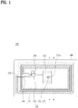
- FIG. 1 is a front view illustrating a sensor 100 according to one embodiment of the present invention
- FIG. 2 is an exploded perspective view illustrating a sensor 100 of FIG. 1 .
- description will be given with reference to FIGS. 1 and 2 together.
- the sensor may comprise a substrate 110, a conductive layer 120, and an insulating layer.
- the conductive layer 120 may include an antenna pattern 121, a sensing electrode 122, and a circuit line 124.
- the substrate 110 configures a non-conductive layer.
- the substrate 110 serves as a target in which the conductive layer 120 is packaged.
- the substrate 110 may include a plastic layer 111 and a silica layer 112.
- the plastic layer 111 is made of plastic (polymer compound or synthetic resin) having flexibility.
- the plastic may include at least one selected from a group of a polyethylene erephthalate (PET), a polyimide (PI), a polystyrene (PS) and a polyethylene naphthalate (PEN).
- the silica layer 112 may be coated on one surface of the plastic layer 111.
- the silica layer 112 may be formed between the plastic layer 111 and the conductive layer 120.
- the silica layer 112 enables fast diffusion of a sensing target material 10, especially solution, stability of the sensing target material 10, and attachment intensity enhancement of the conductive layer 120.
- the silica layer 112 may have a thickness of several nm to several tens of nm.
- the conductive layer 120 may be provided on one surface of the substrate 110.
- the conductive layer 120 may include an antenna pattern 121, a circuit line 124 and a sensing electrode, as described above.
- the sensing electrode 122 causes an impedance change by a contact of the sensing target material 10.
- the impedance change may mean a state of the sensing target material 10.
- sensing electrode 122 Details of the sensing electrode 122 will be described later.
- the antenna pattern 121 transmits or receives a radio signal to or from an external device.
- the antenna pattern 121 may serve to receive a sensing command signal of the external device to measure an impedance change of the sensing target material 10 or transmit the measured impedance change value to the external device.
- the circuit line 124 forms a passage for signal transfer by electrically connecting the antenna pattern 121 with the sensing electrode 122.
- the conductive layer 120 may be formed in a single body.
- the case that the antenna pattern 121, the sensing electrode 122 and the circuit line 124 of the conductive layer 120 are formed in a single body may mean that they are functionally identified from one another but may structurally be formed of the same material by the same process in view of the manufacturing process.
- the coating electrode 123 of the conductive layer 120 may be formed of a hetero-material unlike the other components or implemented by a process different from that of the other components. A detailed description of the coating electrode will be described later.
- the components of the conductive layer 120 may be formed respectively by a separate process without being formed in a single body.
- the conductive layer 120 provided in a single body may not be detachable physically.
- the conductive layer 120 may be formed on the substrate 110 by an electron printing method.
- the conductive layer 120 of the related art is formed by a vacuum deposition method.
- the conductive layer 120 formed by the vacuum deposition method is advantageous in that it has a stable structure but the manufacturing and material costs are increased in that addition process such as etching is required after vacuum deposition, and a shape deformation of the substrate 110 may be caused by the process performed at a high temperature.
- the electronic printing process of the conductive layer 120 may be performed by any one method of Gravure offset, Gravure printing, and Screen printing.
- At least some of the conductive layer 120 may be formed as the same layers.
- the case that at least some of the conductive layer 120 are formed of the same material as the same layers may mean that the conductive layer 120 is printed on the substrate 110 by a printing process of one time in view of the manufacturing process. If the conductive layer 120 is printed by a printing process of one time, the manufacturing process may be simplified, whereby the manufacturing cost and time may be minimized.
- an area of the conductive layer 120 formed as the same layer may include all or some of the antenna pattern 121, and the circuit line 124 and the sensing electrode 122. A detailed description of the conductive layer 120 will be given later.
- the antenna pattern 121 transmits or receives a signal to or from an external device.
- the external device may mean an electronic device having a communication function.
- examples of the external device include a smartphone, a computer, a digital broadcasting terminal, a PDA, etc.
- the sensor 100 may not be provided with a separate power supply unit. This may result in a compact size of the sensor 100 and minimize the manufacturing cost.
- the antenna pattern 121 may be formed on one surface of the substrate 110 two-dimensionally. Particularly, the antenna pattern 121 may be provided along outer corners of the substrate 110 to make sure of an antenna length, and may be provided in a screw shape by being wound several times in accordance with a necessary length. A shape and pattern of the antenna pattern 121 may be change in various ways to implement an antenna function.
- the antenna pattern 121 may have a line width of 500 ⁇ m to 1500 ⁇ m to have high inductance.
- An interval of the antenna pattern 121, which is wound several times, with an adjacent line may be of 300 ⁇ m to 700 ⁇ m to make sure of an appropriate capacitance component.
- the antenna pattern 121 may include a pattern area for performing an original function of an antenna, and a connection area for electrically connecting the pattern area with the circuit line 124 or the sensing electrode 122.
- the pattern area and the connection area may be provided on the same layer, but may be provided on their respective layers different from each other to actively perform electrical connection with the other components.
- an insulating area may additionally be provided to avoid an unintended electrical connection between different layers. A detailed description of the insulating area will be given later.
- the antenna pattern 121 may operate as a radiator of an NFC(Near Field Communication) antenna.
- Information exchange of the NFC antenna may be performed using communication options of 13.56MHz.
- the circuit line 124 electrically connects the antenna pattern 121 with the sensing electrode 122. Also, the circuit line 124 may electrically be connected with a device 150 for controlling the sensor 100. That is, the circuit line 124 may mean all areas except the antenna pattern 121 and the sensing electrode 122 of the conductive layer 120.
- a passivation layer 131 prevents the sensing target material 10 from leaking to the substrate 110 area. Therefore, the sensor 100 is prevented from operating in error due to the sensing target material 10 flowing to the circuit line 124. Also, the passivation layer 131 may have a certain height to prevent the sensing target material from moving. The passivation layer 131 may collect the sensing target material 10 in the sensing electrode 122.
- the passivation layer 131 has a surface energy greater than that of the substrate 110 to allow the sensing target material 10 to form liquid crystals in the passivation layer 131, whereby the sensing target material 10 may not be diffused toward the substrate 110.
- the passivation layer 131 may include a first opening 131a for exposing at least a portion of the sensing electrode 122. Only a partial area exposed through the first opening 131a may be used as the sensing electrode 122.
- the sensing electrode 122 has a total length A of 400 ⁇ m to 5000 ⁇ m, and may be exposed at a length of 50 ⁇ m to 5000 ⁇ m through the first opening 131a. As the case may be, the total length of the sensing electrode 122 may be equal to the length of the sensing electrode 122 exposed through the first opening 131a, or the sensing electrode 122 may partially be exposed through the first opening 131a.
- the length of the sensing electrode 122 exposed through the first opening 131a affects resolution of the sensor 100, printing reproducibility according to mass production and reliability of the sensor 100. The shorter the length of the sensing electrode 122 exposed through the first opening 131a is, the more improved resolution of the sensor 100 may be.
- a width B of the sensing electrode 122 may be provided within the range of 50 ⁇ m to 1000 ⁇ m.
- a too narrow width of the sensing electrode 122 may cause an unstable printing process of the conductive layer 120.
- the width B of the sensing electrode 122 is 50 ⁇ m to 200 ⁇ m for a stable printing process.
- an interval C between the first sensing electrode 122a and the second electrode 122b may be provided within the range of 50 ⁇ m to 3000 ⁇ m.
- the interval C between the first sensing electrode 122a and the second electrode 122b is too wide and the amount of the sensing target material is not enough, it may be difficult to perform exact measurement. That is, the sensing target material should be in contact with the first sensing electrode 122a and the second sensing electrode 122b by forming a liquid drop. Considering this, the interval C between the first sensing electrode 122a and the second electrode 122b is preferably provided within the range of 900 ⁇ m to 1500 ⁇ m.
- a height D of the sensing electrode 122 may be 700nm to 15 ⁇ m.
- the height D of the sensing electrode 122 may affect a thickness of the sensor 100 and durability and reliability of the sensing electrode 122. If the height D of the sensing electrode 122 is lower than 70nm, a problem may occur in that the sensing electrode 122 is lost in accordance with repetition of sensing. Due to a limitation of the printing process and to prevent the thickness of the sensor 100 from being increased, it is preferable that the height of the sensing electrode 122 is lower than 15 ⁇ m.
- An antenna insulating layer 132 and an antenna bridge 140 form a structure for connecting the antenna pattern 121 with the circuit line 124. If the antenna pattern 121 is formed in a screw shape by being wound in the substrate 110, one end of the antenna pattern 121 should be extended toward a direction where the other end of the antenna pattern 121 is provided. The antenna bridge 140 forms this extended area, and the antenna insulating layer 132 may be provided between the antenna bridge 140 and the antenna pattern 121 such that the antenna bridge 140 is not interfered with the antenna pattern 121 printed through the existing printing process.
- a protective layer 160 may be formed of an insulating material and arranged to face one surface of the substrate 110 so as to cover the substrate 110 and all of components packaged in the substrate 110, such as the conductive layer 120 and the passivation layer 131, thereby electrically and physically protecting the corresponding components.
- the protective layer 160 may include a second opening 160a for exposing the first opening 131a of the passivation layer 131.
- a device 150 may be packaged in the substrate 110 and thus electrically connected with the circuit line 124.
- the electronic components may include a power generator, a controller, a converter, and a communication unit.
- the radio signal received through the antenna pattern 121 is transferred to the device 150 through the circuit line 124.
- the device 150 may generate an alternating current power source through the direct current power source supplied thereto and input the generated alternating current power source to the sensing electrode 122.
- FIG. 3 is a cross-sectional view illustrating an area A-A' of FIG. 1
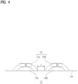
- FIG. 4 is a partially enlarged view illustrating an area A-A' of FIG. 1 .
- description will be given with reference to FIGS. 3 and 4 together.
- the sensing electrode 122 is direction in contact with the sensing target material 10, and if the sensing electrode 122 is formed by a vacuum deposition method, it is sufficient that the area of the sensing electrode 122 is only made of a material such as Pt or Au. However, as described above, if the antenna pattern and the circuit line are configured as the same layer through the electronic printing method, a material cost is too increased.
- This problem may be solved by replacing the sensing electrode 122 with a material such as Ag, Cu and Al.
- Ag, Cu and Al may be provided as main components of the sensing electrode 122.
- the sensing electrode 122 may be made of a combined component of conductive particles 1221 such as Ag, Cu and Al and a binder 1222 of an organic material.
- the conductive particles 1221 may have a spherical shape or a flake shape.
- the flake shaped conductive particles 1221 may have conductivity relatively higher than that of the spherical shaped conductive particles.
- the conductive particles 1221 may have a size of several tens of nm to 20 ⁇ m to make sure of a reaction specific surface area.
- the sensing electrode 122 causes an impedance change by reaction with the sensing target material 10, and a capacitance component and a resistance component exist in the impedance. If the reaction specific surface area of the conductive particles 1221 is widened, oxidation or corrosion of the sensing electrode by reaction may be suppressed, and lifespan of the sensor 100 may be extended.
- the binder 1222 supports the conductive particles 1221.
- the binder 1222 may serve to improve durability and reliability of the sensing electrode 122.
- the binder 1222 may include at least one resin selected from a Polyethylene oxide (PEO) based group, an Oleic acid based group, an Acrylate based group, an Acetate based group and an Epoxy based group.
- PEO Polyethylene oxide
- the sensing electrode 121 may have pores 1213.
- the pores 1213 may have a size of several nm to several tens of ⁇ m. If the sensing electrode 121 has pores 1213, since the sensor 100 is not damaged easily by repeated mechanical deformation, reliability of the sensor 100 may be improved.
- the sensing electrode 122 may form an acute angle with the substrate 110. That is, a corner area of the sensing electrode 122 forms a slow inclination from the substrate 110 so that the sensing electrode 122 is not easily separated from by bending of the substrate 110.
- sensing electrode 122 is exposed to be in contact with the sensing target material 10, a standard reduction potential of a material such as Ag, Cu and Al may be lowered, whereby it is likely that the sensing electrode 122 is corroded. Corrosion of the sensing electrode 122 disturbs a contact between the sensing target material 10 and the sensing electrode 122 and causes occurrence of noise in impedance measurement.
- a surface area of the sensing electrode 122 which is in contact with the sensing target material 10 is reduced due to sizes of the particles of the sensing electrode 122. This reduction of the contact surface area also acts to cause reduce exactness of sensing.
- the coating electrode 123 may be provided outside the sensing electrode 122.
- the coating electrode 123 may additionally be provided on an outer side of the sensing electrode 122 through the electronic printing method such that the sensing electrode 122 may be treated with sensitization.
- the coating electrode 123 serves to increase electric conductivity of the sensing target material 10 and the sensing electrode 122.
- the coating electrode 123 may enhance durability and wear resistance of the sensing electrode 122.
- the conductive particles 1231 of the coating electrode 123 may include a carbon nano tube (CNT).
- CNT carbon nano tube
- the binder 1232 of the coating electrode 123 may minimize a gap 1233 by connecting the conductive particles 1231 of the coating electrode 123.
- the binder of the coating electrode 123 may include at least one resin selected from Polyethylene oxide (PEO) based group, Oleic acid based group, Acrylate based group, Acetate based group and Epoxy based group.
- the conductive particles 1231 of the coating electrode 123 may additionally include Graphite. Graphite serves to enhance conductivity of the sensing electrode 122.
- the conductive particles 1231 of the coating electrode 123 may include a carbon black.
- the carbon black serves to enhance durability or wear resistance of the sensing electrode 122.
- the Graphite and the carbon black may be configured at 10% or more of a total mass of a conductive material.
- the coating electrode 123 may be provided to cover the outer side of the sensing electrode 122. Pores 1223 of the sensing electrode 122 serve to have durability for mechanical deformation of the sensor 100 as described above. On the contrary, the pores 1223 disturbs exact impedance measurement by lowering conductivity of the sensing electrode 122.
- the coating electrode 123 allows the sensing electrode 122 filled with the pores 1223 to have high conductivity, whereby exact impedance can be measured.
- the sensing electrode 122 has two electrodes 122a and 122b spaced apart from each other to be in contact with the sensing target material 10. This case is equally applied to the coating electrode 123.
- the first coating electrode 123a and the second coating electrode 123b of the coating electrode 123 may be spaced apart from each other at an interval of 10 ⁇ m. This value corresponds to an approximate value, and the interval does not require 10 ⁇ m, exactly.
- the thickness of the coating electrode that is, the thickness from the uppermost end of the sensing electrode 122 to the uppermost end of the coating electrode 123 may be 10 ⁇ m or less.
- the aforementioned passivation layer 131 may be provided outside the coating electrode 123. That is, the sensing electrode 122, the coating electrode 123 and the passivation layer 131 may sequentially be deposited at the outside from the substrate 110. Therefore, a length condition of the coating electrode 123 may be applied equally to the length condition of the sensing electrode 122. Therefore, the coating electrode 123 may be exposed to the outside through the first opening 131a as much as the length of the sensing electrode 122.
- a conjugate polymer layer may be used to improve conductivity of the sensing electrode 122.
- the conjugate polymer layer may include a material such as a conductive polymer (PEDOT:PSS/P3HT).
- the conjugate polymer layer may be implemented in the sensing electrode 122 by a patterning process, or may be removed after being absorbed in the sensing electrode 122 for a certain time in a state that it is coated on a front surface.
- the sensing electrode 122 may be pressed through a rolling process. In a state that the sensing electrode 122 is printed, a certain temperature may be increased, and in a state that the increased temperature is maintained, the sensing electrode 122 may be pressed through a roller.
- the sensing electrode 122 is pressed through the rolling process, coupling of the sensing electrode 122 may be broken by pressure. To minimize this phenomenon, a groove may be formed in the roller and then the rolling process may be performed.
- FIG. 5 is a view illustrating a sensor 200 of the present invention, which is linked to an external device 20.
- the external device 20 is a mobile terminal, especially smartphone although the external device 20 may have various types.
- the sensor 200 transmits or receives a radio signal to or from an external device through an antenna pattern 221.
- the sensor 200 generates a direct current power source through a power generator 251 to drive a circuit unit 250.
- the sensor 200 of the present invention does not have a component for power supply but generates a direct current power source by using the radio signal received from the external device 20.
- a controller 252, a converter 253, a communication unit 254 and a sensing electrode 222 are operated by the generated direct current power source.
- the controller 252 is driven by the direct current power source which is supplied.
- the controller 252 generates an alternating current voltage and inputs the generated alternating current voltage to the sensing electrode 222.
- the sensing electrode 222 may refer to a concept that includes a coating electrode 123 (see FIG. 3 ).
- the sensing electrode 222 which will be described later may include a coating electrode.
- the sensing electrode 222 If the sensing electrode 222 is reacted with a sensing target material, the sensing electrode 222 causes an impedance change.
- the impedance change of the sensing electrode 222 is represented by a change of the alternating current voltage generated by the controller 252.
- the sensing target material may be identified in accordance with a range of an output value.
- the external device 20 generates information by receiving the digitalized signal from the sensor 200 and stores and manages the generated information.
- FIG. 6 is a conceptual view illustrating a structure of a circuit line 324, a sensing electrode 322, a coating electrode 323 and a passivation layer 331.
- the sensor is formed by printing, heat drying and hardening processes. Particularly, if the printing process is repeated, a process error, especially alignment error may occur, and an error may occur due to contradiction of the substrate even during the heat drying process.
- the first sensing electrode 322a, the second electrode 322b, the first coating electrode 323a, the second coating electrode 323b, the circuit line 324 and the passivation layer 331 may be formed by the printing process.
- the passivation layer 331 is arranged to cover the first sensing electrode 322a, the second sensing electrode 322b, the first coating electrode 323a, the second coating electrode 323b and the circuit line 324. Therefore, the passivation layer 331 is formed after printing of the sensing electrodes 322a and 322b, the coating electrodes 323a and 323b and the circuit line 324. Therefore, the process error may occur due to repetition of the printing process and during the heat drying process. For this reason, the sensing electrodes 322a and 322b or the coating electrodes 323a and 323b may be exposed or covered unlike a design intention.
- the sensing electrodes 322a and 322b and the coating electrodes 323a and 323b may be partitioned into three parts along a longitudinal direction. These three parts are defined as first end portions 322a1, 322b1, 323a1 and 323b1, second end portions 322a2, 322b2, 323a2 and 323b2, and center portions 322a3, 322b3, 323a3 and 323b3.
- the passivation layer 331 covers the first end portions 322a1, 322b1, 323a1 and 323b1 and the second end portions 322a2, 322b2, 323a2 and 323b2, and the first opening 331a exposes the center portions 322a3, 322b3, 323a3 and 323b3.
- the sensing electrode 322 and the coating electrode 323 are formed to be longer than the length of the first opening 331a.
- the first opening 331a may control the exposed length of the sensing electrode 322 and the coating electrode 323. Therefore, a length G of the first opening 331a of the passivation layer 331 may be controlled accurately to lower an error.
- the sensing electrode 322 and the coating electrode 323 are designed only for the purpose of improving resolution, a problem of durability and reliability may occur. Therefore, considering resolution, durability and reliability, the structure of the sensing electrode 322 and the coating electrode 323 should be designed.
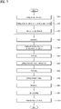
- FIGS. 7 and 8 are flow charts illustrating a manufacturing method for a sensor related to the present invention.
- the conductive layer is printed on the substrate through the printing process (S100).
- the conductive layer includes an antenna pattern, a sensing electrode, a coating electrode and a circuit line.
- the antenna pattern, the sensing electrode and the circuit line are made of the same material, the antenna pattern, the sensing electrode and the circuit line of the conductive layer may be formed simultaneously by a printing process of one time (S110). Therefore, this may reduce material and manufacturing costs. This will be defined as a first printing process for convenience.
- the antenna pattern, the sensing electrode and the circuit line may be provided on the same layer due to the first printing process.
- the coating electrode may be printed on the outer side of the sensing electrode (S120). Since the coating electrode is made of a material different from that of the sensing electrode, the coating electrode may be formed through additional second printing process.
- the coating electrode configures a hetero-layer deposited on a layer provided with the sensing electrode.
- the printing process of the conductive layer uses a powdered ink or paste.
- a composition of the powdered ink or paste may include conductive particles of 40weight% to 70weight%, and an organic material of 30weight% to 60weight% containing solvent. As a result, oxidation and corrosion of the sensing electrode or the coating electrode may be minimized.
- the conductive particles of the sensing electrode may be made of at least one of Ag, CU and Al.
- the conductive particles of the coating electrode may be made of at least one of carbon nano tube, graphite and carbon black.
- the conductive particles of the sensing electrode or the conductive particles of the coating electrode may have a spherical shape or a flake shape.
- a solvent for mixing the conductive particles with the binder may include at least one selected from a group of Acetone, Allyl alcohol, Acetic acid, Acetol, Methyalcohol and Benzene.
- the printing process of the conductive layer 120 may be any one of Screen, offset, and Gravure.
- the conductive layer may be hardened through heat drying (S200). Heat drying may be performed at 80 °C to 200 °C. The aforementioned solvent may be evaporated during heat drying. To enable the process of a low temperature of 200 °C or less, it is preferable that the conductive particles have a size of several tens of nm to 20 ⁇ m in the form of powder.
- heat drying may be performed after a first printing process for printing the sensing electrode and a second printing process for printing the coating electrode.
- the coating electrode As the coating electrode is printed on the sensing electrode prior to heat drying, the coating electrode enters a portion between gaps of the sensing electrode, whereby the sensing electrode and the coating electrode may be coupled to each other more densely. If the sensing electrode and the coating electrode are coupled to each other densely, conductivity is enhanced, and the coating electrode may be prevented from being easily separated from the substrate or the sensing electrode by a high coupling force.
- the heat drying process may be performed primarily and then the second printing process may be performed for the coating electrode.
- the passivation layer and the antenna insulating layer may be printed (S300).
- the passivation layer and the antenna insulating layer may be made of the same material, and therefore may be formed at the same time through one printing process. That is, the passivation layer and the antenna insulating layer may form the same layer on the conductive layer.
- the printed passivation layer and antenna insulating layer may be hardened (S400).
- the passivation layer and the antenna insulating layer may be hardened by ultraviolet (UV) rays.
- the printing processes may be performed multiple times to make sure of sure insulation reliability (S500).
- the antenna insulating layer which is first printed may be defined as a first antenna insulating layer, and the antenna insulating layer which is printed later may be defined as a second antenna insulating layer.
- the second antenna insulating layer may be further hardened in the same manner as the hardening process of the first antenna insulating layer (S600).
- additional antenna insulating layer may be printed. In this case, the same hardening process as that of the first antenna insulating layer or the second antenna insulating layer is performed.
- An antenna bridge is printed on the antenna insulating layer (S700).
- the antenna bridge may be made of the same material as that of the conductive layer.
- the antenna bridge may be heat-dried in the same manner as the conductive layer (S800). Details of a heat drying condition are the same as those described in the heat drying process of the conductive layer.
- the device may be bonded to the substrate (S900).
- the device is electrically connected with the circuit line.
- the protective layer may be covered on the substrate to protect the components packaged in the substrate (S1000).
- FIGS. 9(a) and 9(b) are graphs illustrating that ADC change according to measurement times for each of a sensor of the related art and a sensor of the present invention is measured.
- an ADC value according to measurement times is uniformly maintained without change when Nacl and food are sequentially measured through the sensor of the present invention unlike the sensor of the related art. Therefore, it is noted that a resultant value of high reliability can be obtained by the user of the sensor without the problem of corrosion or durability.
Landscapes
- Chemical & Material Sciences (AREA)
- Engineering & Computer Science (AREA)
- Mechanical Engineering (AREA)
- Analytical Chemistry (AREA)
- Electrochemistry (AREA)
- Physics & Mathematics (AREA)
- Health & Medical Sciences (AREA)
- Life Sciences & Earth Sciences (AREA)
- Chemical Kinetics & Catalysis (AREA)
- Biochemistry (AREA)
- General Health & Medical Sciences (AREA)
- General Physics & Mathematics (AREA)
- Immunology (AREA)
- Pathology (AREA)
- Composite Materials (AREA)
- Investigating Or Analyzing Materials By The Use Of Electric Means (AREA)
Abstract
Description
- The present invention relates to a printing type sensor that senses an impedance change of a target material to measure salinity and a sugar content and determine a denaturalization level of edible oil and fat and transmits the sensed result to simply check the sensed result.
- Generally, a sensor of the related art is provided in the form of a terminal to measure salinity and a sugar content and determine a denaturalization level of edible oil and fat.
- A terminal type sensor has advantages in that measurement and output of a measured result may be performed without a separate device, but should be provided with a separate power supply, whereby a problem occurs in that volume, weight, etc. are increased.
- Particularly, with the trend of increasing users who necessarily use a mobile terminal such as a smartphone, it is considered to replace some functions of a sensor with those of a power supply unit and an output unit of a smartphone.
- Therefore, a portable sensor is required, which performs only a measurement function of a material and transmits the measured result to an external device or receives a sensing signal.
- However, for such a portable sensor, it is necessary to consider a material and structure for obtaining an exact measured value while satisfying a small size.
- In a portable sensor for implementing the material and structure, it is general that a vacuum deposition method is used to form a conductive area such as a sensing electrode. The vacuum deposition method may cause deformation of a substrate due to a process condition of a high temperature and cause increase of the manufacturing cost.
- Therefore, a sensor manufactured by a printing method may be considered to substitute for the vacuum deposition method. Moreover, it is required to solve a corrosion problem and a reliability problem such as durability degradation, which may occur in the sensor of the printing method.
- An object of the present invention is to solve the aforementioned problems of a sensor, in the form of a terminal, not being compact and the problem of high manufacturing costs and low manufacturing quality of a sensor manufactured using a deposition method in order to replace such a sensor with a sensor manufactured by a printing method,
- Another object of the present invention is to provide a sensor by solving a corrosion problem of a sensing electrode, a durability problem, etc. that may occur in a sensor of a printing method.
- According to one aspect of the present invention to achieve the above problems or other problems, there is provided a sensor comprising a non-conductive substrate; and a conductive layer electronically printed on one surface of the substrate, wherein the conductive layer includes an antenna pattern for transmitting or receiving a radio signal to or from an external device; a sensing electrode connected to the antenna pattern through a circuit line, for sensing an impedance change due to a contact with a sensing target material; and a coating electrode deposited on the sensing electrode, for removing an occurrence of noise of the impedance change.
- Also, according to another aspect of the present invention, there is provided a sensor characterized in that each of the sensing electrode and the coating electrode includes a plurality of conductive particles forming a gap, and a binder having the plurality of conductive particles to fill the gap.
- Also, according to another aspect of the present invention, there is provided a sensor characterized in that the conductive particles of the sensing electrode include Ag.
- Also, according to another aspect of the present invention, there is provided a sensor characterized in that the conductive particles of the coating electrode include a carbon nano tube (CNT).
- Also, according to another aspect of the present invention, there is provided a sensor characterized in that the conductive particles of the coating electrode further include a Graphite and a carbon black.
- Also, according to another aspect of the present invention, there is provided a sensor characterized in that the graphite and the carbon black are configured at 10% or less of a total mass of the coating electrode.
- Also, according to another aspect of the present invention, there is provided a sensor characterized in that the binder includes one of a Polyethylene oxide (PEO) based resin, an Oleic acid based resin, an Acrylate based resin, an Acetate based resin, and an Epoxy based resin.
- Also, according to another aspect of the present invention, there is provided a sensor characterized in that the conductive particles are configured by combination of a flake shape or a spherical shape.
- Also, according to another aspect of the present invention, there is provided a sensor characterized in that the antenna pattern, the circuit line and the sensing electrode are made of the same material, provided on the same layer, and the coating electrode is provided by being deposited on the sensing electrode.
- Also, according to another aspect of the present invention, there is provided a sensor characterized in that the sensing electrode includes two electrodes spaced apart from each other, the coating electrode includes a first area and a second area, which respectively cover the spaced electrodes, and a minimum distance between the first area and the second area is 10µm, and a thickness of the coating electrode from an upper end of the sensing electrode is 10µm.
- Also, according to another aspect of the present invention, there is provided a sensor characterized in that the sensing electrode includes two electrodes spaced apart from each other, and an interval between the two electrodes is 30µm or more and 3000µm or less.
- Also, according to another aspect of the present invention, there is provided a sensor characterized in that the antenna pattern, the sensing electrode and the circuit line have a thickness of 0.5µm or more and 15µm or less.
- Also, according to another aspect of the present invention, there is provided a sensor characterized in that the substrate includes any one of polyethylene erephthalate (PET), polyimide (PI), polystyrene (PS) and polyethylene naphthalate (PEN).
- Also, according to another aspect of the present invention, there is provided a sensor characterized in that the antenna pattern has a width of 500µm or more and 1500µm or less, and an adjacent distance of the antenna pattern is 300µm or more and 700µm or less.
- Also, according to another aspect of the present invention, there is provided a sensor further comprising a passivation layer forming an opening, which exposes at least one area of the sensing electrode, having a surface energy greater than that of the substrate.
- Also, according to another aspect of the present invention, there is provided a sensor further comprising a protective layer deposited on the substrate, protecting the conductive layer and the passivation layer.
- Also, according to still another aspect of the present invention, there is provided a sensor comprising a non-conductive substrate; and a conductive layer electronically printed on one surface of the substrate, wherein the conductive layer includes an antenna pattern for transmitting or receiving a radio signal to or from an external device, a sensing electrode connected to the antenna pattern through a circuit line, for sensing an impedance change due to a contact with a sensing target material, and a conjugate polymer layer containing a conductive polymer provided by being patterned or absorbed in the sensing electrode.
- Also, according to further still another aspect of the present invention, there is provided a sensor comprising a non-conductive substrate, and a conductive layer electronically printed on one surface of the substrate, wherein the conductive layer includes an antenna pattern for transmitting or receiving a radio signal to or from an external device, and a sensing electrode connected to the antenna pattern through a circuit line, for sensing an impedance change due to a contact with a sensing target material, and the sensing electrode is pressed through a rolling process.
- Advantageous effects of a sensor according to the present invention are as follows.
- According to at least one of the embodiments of the present invention, a compact sensor linked to an external device may be provided.
- According to at least one of the embodiments of the present invention, a sensor is capable of being manufactured at a low temperature to reduce the probability of occurrence of a defect rate caused by deformation.
- According to at least one of the embodiments of the present invention, a sensor is capable of being manufactured by minimum layers for several conductive components to reduce the manufacturing cost.
- According to at least one of the embodiments of the present invention, a sensor is capable of being manufactured at a low cost through an electronic printing method.
- Further scope of applicability of the present application will become more apparent from the detailed description given hereinafter. However, it should be understood that the detailed description and specific examples, while indicating preferred embodiments of the invention, are given by way of illustration only, since various changes and modifications within the spirit and scope of the invention will become apparent to those skilled in the art from the detailed description.
-
-
FIG. 1 is a front view illustrating a sensor according to one embodiment of the present invention. -
FIG. 2 is an exploded perspective view illustrating a sensor ofFIG. 1 . -
FIG. 3 is a cross-sectional view illustrating an area A-A' ofFIG. 1 . -
FIG. 4 is a partially enlarged view illustrating an area A-A' ofFIG. 1 . -
FIG. 5 is a view illustrating a sensor of the present invention, which is linked to an external device. -
FIG. 6 is a conceptual view illustrating a structure of a circuit line, a sensing electrode, a coating electrode and a passivation layer. -
FIG. 7 is a flow chart illustrating a manufacturing method for a sensor related to the present invention. -
FIG. 8 is a flow chart illustrating another method for a sensor related to the present invention. -
FIGS. 9(a) and 9(b) are graphs illustrating that an ADC change according to measurement times for each of a sensor of the related art and a sensor of the present invention is measured. -
FIG. 1 is a front view illustrating asensor 100 according to one embodiment of the present invention, andFIG. 2 is an exploded perspective view illustrating asensor 100 ofFIG. 1 . For convenience of description, description will be given with reference toFIGS. 1 and2 together. - The sensor may comprise a
substrate 110, aconductive layer 120, and an insulating layer. In this case, theconductive layer 120 may include anantenna pattern 121, asensing electrode 122, and a circuit line 124. - The
substrate 110 configures a non-conductive layer. Thesubstrate 110 serves as a target in which theconductive layer 120 is packaged. For example, thesubstrate 110 may include aplastic layer 111 and asilica layer 112. - The
plastic layer 111 is made of plastic (polymer compound or synthetic resin) having flexibility. The plastic may include at least one selected from a group of a polyethylene erephthalate (PET), a polyimide (PI), a polystyrene (PS) and a polyethylene naphthalate (PEN). - The
silica layer 112 may be coated on one surface of theplastic layer 111. Thesilica layer 112 may be formed between theplastic layer 111 and theconductive layer 120. Thesilica layer 112 enables fast diffusion of asensing target material 10, especially solution, stability of thesensing target material 10, and attachment intensity enhancement of theconductive layer 120. Thesilica layer 112 may have a thickness of several nm to several tens of nm. - The
conductive layer 120 may be provided on one surface of thesubstrate 110. - The
conductive layer 120 may include anantenna pattern 121, a circuit line 124 and a sensing electrode, as described above. - The
sensing electrode 122 causes an impedance change by a contact of thesensing target material 10. The impedance change may mean a state of thesensing target material 10. - Details of the
sensing electrode 122 will be described later. - The
antenna pattern 121 transmits or receives a radio signal to or from an external device. For example, theantenna pattern 121 may serve to receive a sensing command signal of the external device to measure an impedance change of thesensing target material 10 or transmit the measured impedance change value to the external device. - The circuit line 124 forms a passage for signal transfer by electrically connecting the
antenna pattern 121 with thesensing electrode 122. - The
conductive layer 120 may be formed in a single body. The case that theantenna pattern 121, thesensing electrode 122 and the circuit line 124 of theconductive layer 120 are formed in a single body may mean that they are functionally identified from one another but may structurally be formed of the same material by the same process in view of the manufacturing process. However, as the case may be, thecoating electrode 123 of theconductive layer 120 may be formed of a hetero-material unlike the other components or implemented by a process different from that of the other components. A detailed description of the coating electrode will be described later. - Alternatively, if necessary, the components of the
conductive layer 120 may be formed respectively by a separate process without being formed in a single body. - The
conductive layer 120 provided in a single body may not be detachable physically. - The
conductive layer 120 may be formed on thesubstrate 110 by an electron printing method. - The
conductive layer 120 of the related art is formed by a vacuum deposition method. Theconductive layer 120 formed by the vacuum deposition method is advantageous in that it has a stable structure but the manufacturing and material costs are increased in that addition process such as etching is required after vacuum deposition, and a shape deformation of thesubstrate 110 may be caused by the process performed at a high temperature. - The electronic printing process of the
conductive layer 120 may be performed by any one method of Gravure offset, Gravure printing, and Screen printing. - At least some of the
conductive layer 120 may be formed as the same layers. The case that at least some of theconductive layer 120 are formed of the same material as the same layers may mean that theconductive layer 120 is printed on thesubstrate 110 by a printing process of one time in view of the manufacturing process. If theconductive layer 120 is printed by a printing process of one time, the manufacturing process may be simplified, whereby the manufacturing cost and time may be minimized. - In detail, an area of the
conductive layer 120 formed as the same layer may include all or some of theantenna pattern 121, and the circuit line 124 and thesensing electrode 122. A detailed description of theconductive layer 120 will be given later. - The
antenna pattern 121 transmits or receives a signal to or from an external device. - The external device may mean an electronic device having a communication function. For example, examples of the external device include a smartphone, a computer, a digital broadcasting terminal, a PDA, etc.
- The
antenna pattern 121 generates a direct current power source by receiving a radio signal from the external device, wherein the generated direct current power source is used for measurement driving of thesensor 100. A measured impedance difference of thesensing target material 10 may again be transmitted to the external device through theantenna pattern 121. - Since the direct current power source is generated by the
antenna pattern 121, thesensor 100 may not be provided with a separate power supply unit. This may result in a compact size of thesensor 100 and minimize the manufacturing cost. - The
antenna pattern 121 may be formed on one surface of thesubstrate 110 two-dimensionally. Particularly, theantenna pattern 121 may be provided along outer corners of thesubstrate 110 to make sure of an antenna length, and may be provided in a screw shape by being wound several times in accordance with a necessary length. A shape and pattern of theantenna pattern 121 may be change in various ways to implement an antenna function. - The
antenna pattern 121 may have a line width of 500µm to 1500µm to have high inductance. An interval of theantenna pattern 121, which is wound several times, with an adjacent line may be of 300µm to 700µm to make sure of an appropriate capacitance component. - The
antenna pattern 121 may include a pattern area for performing an original function of an antenna, and a connection area for electrically connecting the pattern area with the circuit line 124 or thesensing electrode 122. The pattern area and the connection area may be provided on the same layer, but may be provided on their respective layers different from each other to actively perform electrical connection with the other components. To this end, an insulating area may additionally be provided to avoid an unintended electrical connection between different layers. A detailed description of the insulating area will be given later. - The
antenna pattern 121 may operate as a radiator of an NFC(Near Field Communication) antenna. Information exchange of the NFC antenna may be performed using communication options of 13.56MHz. - The circuit line 124 electrically connects the
antenna pattern 121 with thesensing electrode 122. Also, the circuit line 124 may electrically be connected with adevice 150 for controlling thesensor 100. That is, the circuit line 124 may mean all areas except theantenna pattern 121 and thesensing electrode 122 of theconductive layer 120. - A
passivation layer 131 prevents thesensing target material 10 from leaking to thesubstrate 110 area. Therefore, thesensor 100 is prevented from operating in error due to thesensing target material 10 flowing to the circuit line 124. Also, thepassivation layer 131 may have a certain height to prevent the sensing target material from moving. Thepassivation layer 131 may collect thesensing target material 10 in thesensing electrode 122. - The
passivation layer 131 has a surface energy greater than that of thesubstrate 110 to allow thesensing target material 10 to form liquid crystals in thepassivation layer 131, whereby thesensing target material 10 may not be diffused toward thesubstrate 110. - The
passivation layer 131 may include afirst opening 131a for exposing at least a portion of thesensing electrode 122. Only a partial area exposed through thefirst opening 131a may be used as thesensing electrode 122. - The
sensing electrode 122 has a total length A of 400µm to 5000µm, and may be exposed at a length of 50µm to 5000µm through thefirst opening 131a. As the case may be, the total length of thesensing electrode 122 may be equal to the length of thesensing electrode 122 exposed through thefirst opening 131a, or thesensing electrode 122 may partially be exposed through thefirst opening 131a. - The length of the
sensing electrode 122 exposed through thefirst opening 131a affects resolution of thesensor 100, printing reproducibility according to mass production and reliability of thesensor 100. The shorter the length of thesensing electrode 122 exposed through thefirst opening 131a is, the more improved resolution of thesensor 100 may be. - A width B of the
sensing electrode 122 may be provided within the range of 50µm to 1000µm. The narrower the width B of thesensing electrode 122 is, the more improved resolution of thesensor 100 may be. However, a too narrow width of thesensing electrode 122 may cause an unstable printing process of theconductive layer 120. Preferably, the width B of thesensing electrode 122 is 50µm to 200µm for a stable printing process. - Supposing that both poles of the
sensing electrode 122 are afirst sensing electrode 122a and asecond sensing electrode 122b, an interval C between thefirst sensing electrode 122a and thesecond electrode 122b may be provided within the range of 50µm to 3000µm. - However, if the interval C between the
first sensing electrode 122a and thesecond electrode 122b is too wide and the amount of the sensing target material is not enough, it may be difficult to perform exact measurement. That is, the sensing target material should be in contact with thefirst sensing electrode 122a and thesecond sensing electrode 122b by forming a liquid drop. Considering this, the interval C between thefirst sensing electrode 122a and thesecond electrode 122b is preferably provided within the range of 900µm to 1500µm. - A height D of the
sensing electrode 122 may be 700nm to 15µm. The height D of thesensing electrode 122 may affect a thickness of thesensor 100 and durability and reliability of thesensing electrode 122. If the height D of thesensing electrode 122 is lower than 70nm, a problem may occur in that thesensing electrode 122 is lost in accordance with repetition of sensing. Due to a limitation of the printing process and to prevent the thickness of thesensor 100 from being increased, it is preferable that the height of thesensing electrode 122 is lower than 15µm. - An
antenna insulating layer 132 and anantenna bridge 140 form a structure for connecting theantenna pattern 121 with the circuit line 124. If theantenna pattern 121 is formed in a screw shape by being wound in thesubstrate 110, one end of theantenna pattern 121 should be extended toward a direction where the other end of theantenna pattern 121 is provided. Theantenna bridge 140 forms this extended area, and theantenna insulating layer 132 may be provided between theantenna bridge 140 and theantenna pattern 121 such that theantenna bridge 140 is not interfered with theantenna pattern 121 printed through the existing printing process. - A
protective layer 160 may be formed of an insulating material and arranged to face one surface of thesubstrate 110 so as to cover thesubstrate 110 and all of components packaged in thesubstrate 110, such as theconductive layer 120 and thepassivation layer 131, thereby electrically and physically protecting the corresponding components. However, theprotective layer 160 may include asecond opening 160a for exposing thefirst opening 131a of thepassivation layer 131. - A
device 150 may be packaged in thesubstrate 110 and thus electrically connected with the circuit line 124. - Various electronic components related to operation of the
sensor 100 may be implemented by thedevice 150. The electronic components, for example, may include a power generator, a controller, a converter, and a communication unit. - The radio signal received through the
antenna pattern 121 is transferred to thedevice 150 through the circuit line 124. Thedevice 150 may generate an alternating current power source through the direct current power source supplied thereto and input the generated alternating current power source to thesensing electrode 122. -
FIG. 3 is a cross-sectional view illustrating an area A-A' ofFIG. 1 , andFIG. 4 is a partially enlarged view illustrating an area A-A' ofFIG. 1 . For convenience of description, description will be given with reference toFIGS. 3 and4 together. - The
sensing electrode 122 is direction in contact with thesensing target material 10, and if thesensing electrode 122 is formed by a vacuum deposition method, it is sufficient that the area of thesensing electrode 122 is only made of a material such as Pt or Au. However, as described above, if the antenna pattern and the circuit line are configured as the same layer through the electronic printing method, a material cost is too increased. - This problem may be solved by replacing the
sensing electrode 122 with a material such as Ag, Cu and Al. - That is, Ag, Cu and Al may be provided as main components of the
sensing electrode 122. - The
sensing electrode 122 may be made of a combined component ofconductive particles 1221 such as Ag, Cu and Al and abinder 1222 of an organic material. Theconductive particles 1221 may have a spherical shape or a flake shape. The flake shapedconductive particles 1221 may have conductivity relatively higher than that of the spherical shaped conductive particles. - The
conductive particles 1221 may have a size of several tens of nm to 20µm to make sure of a reaction specific surface area. Thesensing electrode 122 causes an impedance change by reaction with thesensing target material 10, and a capacitance component and a resistance component exist in the impedance. If the reaction specific surface area of theconductive particles 1221 is widened, oxidation or corrosion of the sensing electrode by reaction may be suppressed, and lifespan of thesensor 100 may be extended. - The
binder 1222 supports theconductive particles 1221. Thebinder 1222 may serve to improve durability and reliability of thesensing electrode 122. - The
binder 1222 may include at least one resin selected from a Polyethylene oxide (PEO) based group, an Oleic acid based group, an Acrylate based group, an Acetate based group and an Epoxy based group. - The
sensing electrode 121 may have pores 1213. The pores 1213 may have a size of several nm to several tens of µm. If thesensing electrode 121 has pores 1213, since thesensor 100 is not damaged easily by repeated mechanical deformation, reliability of thesensor 100 may be improved. - The
sensing electrode 122 may form an acute angle with thesubstrate 110. That is, a corner area of thesensing electrode 122 forms a slow inclination from thesubstrate 110 so that thesensing electrode 122 is not easily separated from by bending of thesubstrate 110. - However, if the
sensing electrode 122 is exposed to be in contact with thesensing target material 10, a standard reduction potential of a material such as Ag, Cu and Al may be lowered, whereby it is likely that thesensing electrode 122 is corroded. Corrosion of thesensing electrode 122 disturbs a contact between thesensing target material 10 and thesensing electrode 122 and causes occurrence of noise in impedance measurement. - Also, a surface area of the
sensing electrode 122 which is in contact with thesensing target material 10 is reduced due to sizes of the particles of thesensing electrode 122. This reduction of the contact surface area also acts to cause reduce exactness of sensing. - Three types of embodiments for improving conductivity and reliability and durability of conductive sensing due to the configuration of the
sensing electrode 122 will be described later. - The
coating electrode 123 may be provided outside thesensing electrode 122. - The
coating electrode 123 may additionally be provided on an outer side of thesensing electrode 122 through the electronic printing method such that thesensing electrode 122 may be treated with sensitization. - The possibility of occurrence of noise in an impedance change sensed by the
sensing electrode 122 is reduced due to thecoating electrode 123. That is, thecoating electrode 123 serves to increase electric conductivity of thesensing target material 10 and thesensing electrode 122. - Moreover, the
coating electrode 123 may enhance durability and wear resistance of thesensing electrode 122. - The
coating electrode 123 may be provided to be similar to thesensing electrode 122. That is, thecoating electrode 123 may be provided by combination ofconductive particles 1231 and abinder 1232. - The
conductive particles 1231 of thecoating electrode 123 may include a carbon nano tube (CNT). - The
binder 1232 of thecoating electrode 123 may minimize agap 1233 by connecting theconductive particles 1231 of thecoating electrode 123. The binder of thecoating electrode 123 may include at least one resin selected from Polyethylene oxide (PEO) based group, Oleic acid based group, Acrylate based group, Acetate based group and Epoxy based group. - However, if the
conductive particles 1231 of thecoating electrode 123 are made of a carbon nano tube only, since resistance is high, sensing resolution is degraded. Therefore, theconductive particles 1231 of thecoating electrode 123 may additionally include Graphite. Graphite serves to enhance conductivity of thesensing electrode 122. - Also, the
conductive particles 1231 of thecoating electrode 123 may include a carbon black. The carbon black serves to enhance durability or wear resistance of thesensing electrode 122. - The Graphite and the carbon black may be configured at 10% or more of a total mass of a conductive material.
- The carbon nano tube, the graphite and the carbon black of the
conductive particles 1231 perform the above functions by being organically associated with one another without performing each function independently. - The
coating electrode 123 may be provided to cover the outer side of thesensing electrode 122.Pores 1223 of thesensing electrode 122 serve to have durability for mechanical deformation of thesensor 100 as described above. On the contrary, thepores 1223 disturbs exact impedance measurement by lowering conductivity of thesensing electrode 122. Thecoating electrode 123 allows thesensing electrode 122 filled with thepores 1223 to have high conductivity, whereby exact impedance can be measured. - As described above, the
sensing electrode 122 has twoelectrodes sensing target material 10. This case is equally applied to thecoating electrode 123. - The
first coating electrode 123a and thesecond coating electrode 123b of thecoating electrode 123 may be spaced apart from each other at an interval of 10µm. This value corresponds to an approximate value, and the interval does not require 10µm, exactly. - The thickness of the coating electrode, that is, the thickness from the uppermost end of the
sensing electrode 122 to the uppermost end of thecoating electrode 123 may be 10µm or less. - The
aforementioned passivation layer 131 may be provided outside thecoating electrode 123. That is, thesensing electrode 122, thecoating electrode 123 and thepassivation layer 131 may sequentially be deposited at the outside from thesubstrate 110. Therefore, a length condition of thecoating electrode 123 may be applied equally to the length condition of thesensing electrode 122. Therefore, thecoating electrode 123 may be exposed to the outside through thefirst opening 131a as much as the length of thesensing electrode 122. - Unlike the aforementioned coating electrode, a conjugate polymer layer may be used to improve conductivity of the
sensing electrode 122. The conjugate polymer layer may include a material such as a conductive polymer (PEDOT:PSS/P3HT). The conjugate polymer layer may be implemented in thesensing electrode 122 by a patterning process, or may be removed after being absorbed in thesensing electrode 122 for a certain time in a state that it is coated on a front surface. - To improve conductivity of the
sensing electrode 122 and maintain measurement reliability, thesensing electrode 122 may be pressed through a rolling process. In a state that thesensing electrode 122 is printed, a certain temperature may be increased, and in a state that the increased temperature is maintained, thesensing electrode 122 may be pressed through a roller. - However, if the
sensing electrode 122 is pressed through the rolling process, coupling of thesensing electrode 122 may be broken by pressure. To minimize this phenomenon, a groove may be formed in the roller and then the rolling process may be performed. -
FIG. 5 is a view illustrating asensor 200 of the present invention, which is linked to anexternal device 20. - Hereinafter, a description will be given based on the sensor type of the embodiment 1 unless mentioned separately. However, the description may equally be applied to the embodiments 2 and 3 within the range that does not depart from contradiction.
- A description will be given based on that the
external device 20 is a mobile terminal, especially smartphone although theexternal device 20 may have various types. - The
sensor 200 transmits or receives a radio signal to or from an external device through anantenna pattern 221. - The
sensor 200 generates a direct current power source through apower generator 251 to drive acircuit unit 250. In this way, thesensor 200 of the present invention does not have a component for power supply but generates a direct current power source by using the radio signal received from theexternal device 20. A controller 252, aconverter 253, acommunication unit 254 and asensing electrode 222 are operated by the generated direct current power source. - The controller 252 is driven by the direct current power source which is supplied. The controller 252 generates an alternating current voltage and inputs the generated alternating current voltage to the
sensing electrode 222. Based on the case of the embodiment 1, thesensing electrode 222 may refer to a concept that includes a coating electrode 123 (seeFIG. 3 ). Thesensing electrode 222 which will be described later may include a coating electrode. - If the
sensing electrode 222 is reacted with a sensing target material, thesensing electrode 222 causes an impedance change. The impedance change of thesensing electrode 222 is represented by a change of the alternating current voltage generated by the controller 252. The sensing target material may be identified in accordance with a range of an output value. - The change of the alternating current voltage may be changed to a digital signal. The converter 252 converts the change of the alternating current voltage represented based on the impedance change of the
sensing electrode 222 to a digital signal. Thecommunication unit 254 transmits the digitalized signal to theexternal device 20 through the antenna pattern. In this case, thecommunication unit 254 may be NFC Tag IC. - The
external device 20 generates information by receiving the digitalized signal from thesensor 200 and stores and manages the generated information. - The
external device 20 may display information through a display. -
FIG. 6 is a conceptual view illustrating a structure of acircuit line 324, a sensing electrode 322, a coating electrode 323 and a passivation layer 331. - The sensor is formed by printing, heat drying and hardening processes. Particularly, if the printing process is repeated, a process error, especially alignment error may occur, and an error may occur due to contradiction of the substrate even during the heat drying process.
- Resolution of the sensor may be determined in accordance with an exposed length of first and
second sensing electrodes second sensing electrodes - The
first sensing electrode 322a, thesecond electrode 322b, thefirst coating electrode 323a, thesecond coating electrode 323b, thecircuit line 324 and the passivation layer 331 may be formed by the printing process. The passivation layer 331 is arranged to cover thefirst sensing electrode 322a, thesecond sensing electrode 322b, thefirst coating electrode 323a, thesecond coating electrode 323b and thecircuit line 324. Therefore, the passivation layer 331 is formed after printing of thesensing electrodes coating electrodes circuit line 324. Therefore, the process error may occur due to repetition of the printing process and during the heat drying process. For this reason, thesensing electrodes coating electrodes - The
sensing electrodes coating electrodes first opening 331a exposes the center portions 322a3, 322b3, 323a3 and 323b3. - The sensing electrode 322 and the coating electrode 323 are formed to be longer than the length of the
first opening 331a. Thefirst opening 331a may control the exposed length of the sensing electrode 322 and the coating electrode 323. Therefore, a length G of thefirst opening 331a of the passivation layer 331 may be controlled accurately to lower an error. - It is preferable that a width H of the
first opening 331a is wider than an interval between thefirst electrodes second electrodes first opening 331a is too wide, a sensing target material, which will be in contact with the sensing electrode 322 or the coating electrode 323, may be diffused without forming a liquid drop. - Referring to an experimental result, the shorter the length of the sensing electrode 322 or the coating electrode 323 exposed through the first opening 331 is, the narrower the width of the sensing electrode 322 or the coating electrode 323 is, and the wider the interval between the two electrodes is, the more improved resolution is. However, if the sensing electrode 322 and the coating electrode 323 are designed only for the purpose of improving resolution, a problem of durability and reliability may occur. Therefore, considering resolution, durability and reliability, the structure of the sensing electrode 322 and the coating electrode 323 should be designed.
-
FIGS. 7 and8 are flow charts illustrating a manufacturing method for a sensor related to the present invention. - Referring to
FIG. 7 , the conductive layer is printed on the substrate through the printing process (S100). The conductive layer includes an antenna pattern, a sensing electrode, a coating electrode and a circuit line. - If the antenna pattern, the sensing electrode and the circuit line are made of the same material, the antenna pattern, the sensing electrode and the circuit line of the conductive layer may be formed simultaneously by a printing process of one time (S110). Therefore, this may reduce material and manufacturing costs. This will be defined as a first printing process for convenience. The antenna pattern, the sensing electrode and the circuit line may be provided on the same layer due to the first printing process.
- Afterwards, the coating electrode may be printed on the outer side of the sensing electrode (S120). Since the coating electrode is made of a material different from that of the sensing electrode, the coating electrode may be formed through additional second printing process.
- Therefore, the coating electrode configures a hetero-layer deposited on a layer provided with the sensing electrode.
- The printing process of the conductive layer uses a powdered ink or paste. A composition of the powdered ink or paste may include conductive particles of 40weight% to 70weight%, and an organic material of 30weight% to 60weight% containing solvent. As a result, oxidation and corrosion of the sensing electrode or the coating electrode may be minimized.
- As described above, the conductive particles of the sensing electrode may be made of at least one of Ag, CU and Al. Meanwhile, the conductive particles of the coating electrode may be made of at least one of carbon nano tube, graphite and carbon black.
- The conductive particles of the sensing electrode or the conductive particles of the coating electrode may have a spherical shape or a flake shape.
- A solvent for mixing the conductive particles with the binder may include at least one selected from a group of Acetone, Allyl alcohol, Acetic acid, Acetol, Methyalcohol and Benzene.
- The printing process of the
conductive layer 120 may be any one of Screen, offset, and Gravure. - After the printing process, the conductive layer may be hardened through heat drying (S200). Heat drying may be performed at 80 °C to 200 °C. The aforementioned solvent may be evaporated during heat drying. To enable the process of a low temperature of 200 °C or less, it is preferable that the conductive particles have a size of several tens of nm to 20µm in the form of powder.
- Particularly, heat drying may be performed after a first printing process for printing the sensing electrode and a second printing process for printing the coating electrode. As the coating electrode is printed on the sensing electrode prior to heat drying, the coating electrode enters a portion between gaps of the sensing electrode, whereby the sensing electrode and the coating electrode may be coupled to each other more densely. If the sensing electrode and the coating electrode are coupled to each other densely, conductivity is enhanced, and the coating electrode may be prevented from being easily separated from the substrate or the sensing electrode by a high coupling force.
- Alternatively, as shown in
FIG. 8 , after the first printing process of the sensing electrode, the heat drying process may be performed primarily and then the second printing process may be performed for the coating electrode. - After the heat drying process is completed for both the first printing process and the second printing process, the passivation layer and the antenna insulating layer may be printed (S300).
- The passivation layer and the antenna insulating layer may be made of the same material, and therefore may be formed at the same time through one printing process. That is, the passivation layer and the antenna insulating layer may form the same layer on the conductive layer.
- The printed passivation layer and antenna insulating layer may be hardened (S400). The passivation layer and the antenna insulating layer may be hardened by ultraviolet (UV) rays.
- The printing processes may be performed multiple times to make sure of sure insulation reliability (S500). At this time, the antenna insulating layer which is first printed may be defined as a first antenna insulating layer, and the antenna insulating layer which is printed later may be defined as a second antenna insulating layer. After the second antenna insulating layer is printed, the second antenna insulating layer may be further hardened in the same manner as the hardening process of the first antenna insulating layer (S600).
- If necessary, in addition to the first antenna insulating layer and the second antenna insulating layer, additional antenna insulating layer may be printed. In this case, the same hardening process as that of the first antenna insulating layer or the second antenna insulating layer is performed.
- An antenna bridge is printed on the antenna insulating layer (S700). The antenna bridge may be made of the same material as that of the conductive layer.
- The antenna bridge may be heat-dried in the same manner as the conductive layer (S800). Details of a heat drying condition are the same as those described in the heat drying process of the conductive layer.
- Next, the device may be bonded to the substrate (S900). The device is electrically connected with the circuit line.
- Afterwards, the protective layer may be covered on the substrate to protect the components packaged in the substrate (S1000).
-
FIGS. 9(a) and 9(b) are graphs illustrating that ADC change according to measurement times for each of a sensor of the related art and a sensor of the present invention is measured. - As shown, it is noted that an ADC value according to measurement times is uniformly maintained without change when Nacl and food are sequentially measured through the sensor of the present invention unlike the sensor of the related art. Therefore, it is noted that a resultant value of high reliability can be obtained by the user of the sensor without the problem of corrosion or durability.
- It will be apparent to those skilled in the art that the present specification can be embodied in other specific forms without departing from the spirit and essential characteristics of the specification.
- The above embodiments are therefore to be construed in all aspects as illustrative and not restrictive. The scope of the specification should be determined by reasonable interpretation of the appended claims and all change which comes within the equivalent scope of the specification are included in the scope of the specification.
- As described above, the present invention is fully or partially applicable to all sensors.
Claims (20)
- A sensor comprising:a non-conductive substrate; anda conductive layer electronically printed on one surface of the substrate,wherein the conductive layer includes:an antenna pattern for transmitting or receiving a radio signal to or from an external device;a sensing electrode connected to the antenna pattern through a circuit line, for sensing an impedance change due to a contact with a sensing target material; anda coating electrode deposited on the sensing electrode, for removing an occurrence of noise of the impedance change.
- The sensor of claim 1, wherein each of the sensing electrode and the coating electrode includes:a plurality of conductive particles forming a gap; anda binder having the plurality of conductive particles to fill the gap.
- The sensor of claim 2, wherein the conductive particles of the sensing electrode include Ag.
- The sensor of claim 2, wherein the conductive particles of the coating electrode include a carbon nano tube (CNT).
- The sensor of claim 4, wherein the conductive particles of the coating electrode further include a Graphite and a carbon black.
- The sensor of claim 5, wherein the graphite and the carbon black are configured at 10% or less of a total mass of the coating electrode.
- The sensor of claim 2, wherein the binder includes one of a Polyethylene oxide (PEO) based resin, an Oleic acid based resin, an Acrylate based resin, an Acetate based resin and an Epoxy based resin.
- The sensor of claim 2, wherein the conductive particles are configured by combination of a flake or spherical shape.
- The sensor of claim 1, wherein the antenna pattern, the circuit line and the sensing electrode are made of the same material, provided on the same layer, and the coating electrode is provided by being deposited on the sensing electrode.
- The sensor of claim 1, wherein the sensing electrode includes two electrodes spaced apart from each other, the coating electrode includes a first area and a second area, which respectively cover the spaced electrodes, and a minimum distance between the first area and the second area is 10µm, and a thickness of the coating electrode from an upper end of the sensing electrode is 10µm.
- The sensor of claim 1, wherein the sensing electrode includes two electrodes spaced apart from each other, and an interval between the two electrodes is 30µm or more and 3000µm or less.
- The sensor of claim 10, wherein the antenna pattern, the sensing electrode and the circuit line have a thickness of 0.5µm or more and 15µm or less.
- The sensor of claim 1, wherein the substrate includes any one of polyethylene erephthalate (PET), polyimide (PI), polystyrene (PS) and polyethylene naphthalate (PEN).
- The sensor of claim 1, wherein the antenna pattern has a width of 500µm or more and 1500µm or less, and an adjacent distance of the antenna pattern is 300µm or more and 700µm or less.
- The sensor of claim 1, further comprising a passivation layer forming an opening, which exposes at least one area of the sensing electrode, having a surface energy greater than that of the substrate.
- The sensor of claim 15, further comprising a protective layer deposited on the substrate, protecting the conductive layer and the passivation layer.
- A sensor comprising:a non-conductive substrate; anda conductive layer electronically printed on one surface of the substrate,wherein the conductive layer includes:an antenna pattern for transmitting or receiving a radio signal to or from an external device;a sensing electrode connected to the antenna pattern through a circuit line, for sensing an impedance change due to a contact with a sensing target material; anda conjugate polymer layer containing a conductive polymer provided by being patterned or absorbed in the sensing electrode.
- A sensor comprising:a non-conductive substrate; anda conductive layer electronically printed on one surface of the substrate,wherein the conductive layer includes:an antenna pattern for transmitting or receiving a radio signal to or from an external device; anda sensing electrode connected to the antenna pattern through a circuit line, for sensing an impedance change due to a contact with a sensing target material, andthe sensing electrode is pressed through a rolling process.
- A manufacturing method of a sensor, comprising:a first printing step of printing, on a non-conductive substrate, a sensing electrode connected with the antenna pattern through an antenna pattern for transmitting or receiving a radio signal to or from an external device and a circuit line, sensing an impedance change due to a contact of a sensing target material; anda second printing step of printing a coating electrode for removing occurrence of a noise of the impedance change on an outer side of the sensing electrode; anda drying step of heat drying the printed antenna pattern, sensing electrode and coating electrode.
- The manufacturing method of claim 19, wherein the first printing step and the second printing step are performed by any one of a Gravure offset process, a Gravure printing process and a Screen printing process.
Applications Claiming Priority (3)
| Application Number | Priority Date | Filing Date | Title |
|---|---|---|---|
| US201762445206P | 2017-01-11 | 2017-01-11 | |
| KR1020170154814A KR102024608B1 (en) | 2017-01-11 | 2017-11-20 | Sensor |
| PCT/KR2017/015121 WO2018131818A1 (en) | 2017-01-11 | 2017-12-20 | Sensor |
Publications (3)
| Publication Number | Publication Date |
|---|---|
| EP3570019A1 true EP3570019A1 (en) | 2019-11-20 |
| EP3570019A4 EP3570019A4 (en) | 2020-10-28 |
| EP3570019B1 EP3570019B1 (en) | 2025-07-23 |
Family
ID=63058575
Family Applications (1)
| Application Number | Title | Priority Date | Filing Date |
|---|---|---|---|
| EP17891892.6A Active EP3570019B1 (en) | 2017-01-11 | 2017-12-20 | Sensor |
Country Status (4)
| Country | Link |
|---|---|
| US (1) | US10996181B2 (en) |
| EP (1) | EP3570019B1 (en) |
| KR (1) | KR102024608B1 (en) |
| CN (1) | CN110168357B (en) |
Families Citing this family (5)
| Publication number | Priority date | Publication date | Assignee | Title |
|---|---|---|---|---|
| US10746682B2 (en) * | 2014-10-08 | 2020-08-18 | Rfmicron, Inc. | Wireless sensor with multiple sensing options |
| KR102093697B1 (en) * | 2018-10-01 | 2020-03-26 | 한국과학기술연구원 | Sensor using measurement of impedance and sensing method thereof |
| KR101994165B1 (en) * | 2018-10-04 | 2019-06-28 | 쓰리에이로직스(주) | Nfc salinity sensing module including salinity sensor |
| US11933754B2 (en) | 2018-12-06 | 2024-03-19 | Lg Electronics Inc. | Sensor and method for operating sensor |
| KR102908067B1 (en) * | 2025-09-22 | 2026-01-05 | 디에이치 주식회사 | 3-layer multi-sensor and its manufacturing method |
Family Cites Families (28)
| Publication number | Priority date | Publication date | Assignee | Title |
|---|---|---|---|---|
| US5185256A (en) * | 1985-06-21 | 1993-02-09 | Matsushita Electric Industrial Co., Ltd. | Method for making a biosensor |
| KR19980081191A (en) * | 1997-04-08 | 1998-11-25 | 모리시다요이치 | Conductive paste, manufacturing method thereof and printed wiring board using the same |
| US6103033A (en) * | 1998-03-04 | 2000-08-15 | Therasense, Inc. | Process for producing an electrochemical biosensor |
| DE19901183C2 (en) * | 1999-01-14 | 2001-01-25 | Sensotherm Temperatursensorik | Platinum temperature sensor and manufacturing method for the same |
| FR2789822B1 (en) * | 1999-02-12 | 2001-06-08 | Thomson Csf | SURFACE WAVE DEVICE CONNECTED TO A BASE WITH A CONDUCTIVE ADHESIVE |
| KR100351810B1 (en) * | 1999-12-13 | 2002-09-11 | 엘지전자 주식회사 | absolute humidity sensor |
| US6746584B1 (en) * | 1999-12-15 | 2004-06-08 | Delphi Technologies, Inc. | Oxygen sensing device |
| DE10015430C1 (en) * | 2000-03-28 | 2001-05-10 | Preh Elektro Feinmechanik | Capacitive sensor for detecting surface condensation, has passivation layer covering metallized capacitor electrodes covered by hydrophilic layer |
| US20050236182A1 (en) * | 2002-06-04 | 2005-10-27 | Noriki Hayashi | Board for printed wiring, printed wiring board, and method for manufacturing them |
| WO2004113903A1 (en) * | 2003-06-19 | 2004-12-29 | Arkray, Inc. | Analysis implement with opening in insulation film |
| JP2006078280A (en) * | 2004-09-08 | 2006-03-23 | Denso Corp | Capacitive humidity sensor |
| CN1696680A (en) * | 2005-06-08 | 2005-11-16 | 浙江大学 | Chromatography test method for sheet plate based on impedance measurement, and chromatography test device for sheet plate |
| KR100713333B1 (en) * | 2006-01-04 | 2007-05-04 | 엘에스전선 주식회사 | Multilayer anisotropic conductive film |
| KR100776393B1 (en) * | 2006-04-17 | 2007-11-28 | 주식회사 인포피아 | Biosensor and its manufacturing method |
| KR100799810B1 (en) * | 2007-02-01 | 2008-01-31 | 유도준 | Board-integrated gas sensor capable of stacking and parallel mounting |
| DE102008011601A1 (en) * | 2008-02-28 | 2009-09-03 | Raumedic Ag | Patient data sensor device |
| EP2275805A1 (en) * | 2009-07-16 | 2011-01-19 | Acreo AB | Moister sensor |
| US9759688B2 (en) | 2012-03-01 | 2017-09-12 | Georgia Tech Research Corporation | Highly sensitive standoff gas sensing using carbon nanotubes and integrated wireless devices |
| JP6313744B2 (en) * | 2012-03-23 | 2018-04-18 | エルジー イノテック カンパニー リミテッド | Wireless power receiver |
| WO2013154713A1 (en) * | 2012-04-12 | 2013-10-17 | Unipixel Display, Inc. | Low-visibility antennas based flexographic printing |
| JP6014680B2 (en) * | 2012-11-19 | 2016-10-25 | タツタ電線株式会社 | Laminated film and shield printed wiring board |
| GB2514846B (en) * | 2013-06-07 | 2015-09-30 | Lifescan Scotland Ltd | Electrochemical-based analytical test strip with a soluble electrochemically-active coating opposite a bare electrode |
| WO2014197984A1 (en) * | 2013-06-14 | 2014-12-18 | Ning Yan | Radio frequency identification (rfid) devices for detecting volatile substances |
| KR102087038B1 (en) * | 2013-07-22 | 2020-03-10 | 삼성전자주식회사 | Bio-sensor |
| KR101559215B1 (en) * | 2013-12-31 | 2015-10-15 | 재단법인 다차원 스마트 아이티 융합시스템 연구단 | Biosensor package and packaging method thereof |
| WO2016018030A1 (en) * | 2014-07-31 | 2016-02-04 | 동우 화인켐 주식회사 | Film touch sensor and manufacturing method therefor |
| KR20160132750A (en) * | 2015-05-11 | 2016-11-21 | 삼성전자주식회사 | Electrode structure of biosenor and biosnesor comprising that |
| CN205506739U (en) * | 2016-03-23 | 2016-08-24 | 北京科百宏业科技有限公司 | Humidity sensor |
-
2017
- 2017-11-20 KR KR1020170154814A patent/KR102024608B1/en active Active
- 2017-12-20 US US16/473,212 patent/US10996181B2/en active Active
- 2017-12-20 CN CN201780082997.1A patent/CN110168357B/en active Active
- 2017-12-20 EP EP17891892.6A patent/EP3570019B1/en active Active
Also Published As
| Publication number | Publication date |
|---|---|
| KR20180082949A (en) | 2018-07-19 |
| US20190331623A1 (en) | 2019-10-31 |
| CN110168357B (en) | 2022-07-08 |
| US10996181B2 (en) | 2021-05-04 |
| KR102024608B1 (en) | 2019-09-24 |
| EP3570019A4 (en) | 2020-10-28 |
| EP3570019B1 (en) | 2025-07-23 |
| CN110168357A (en) | 2019-08-23 |
Similar Documents
| Publication | Publication Date | Title |
|---|---|---|
| EP3570019B1 (en) | Sensor | |
| CN107560766B (en) | Piezoresistive sensor and pressure-sensitive element for a piezoresistive sensor | |
| US20180022951A1 (en) | Electroconductive silver paste | |
| CN101136285A (en) | Solid electrolysis capacitor and manufacturing method thereof | |
| Hajiaghajani et al. | Amphibious epidermal area networks for uninterrupted wireless data and power transfer | |
| JP2007534780A5 (en) | ||
| KR102018680B1 (en) | Touch input device including display panel formed with strain gauge and display panel formed with strain gauge forming method | |
| TW200511329A (en) | Forming electrically conductive layers by ink printing | |
| KR20170045963A (en) | A sensor and method for manufacturing the sensor | |
| US20170110781A1 (en) | Sensor and method for manufacturing the sensor | |
| EP3706166A1 (en) | Integrated circuit, method for manufacturing same, and radio communication device using same | |
| CN101261560A (en) | Touch screen electrode preparation method | |
| KR101129924B1 (en) | Method for fabricating water level sensor | |
| Pereira et al. | All‐Printed Smart Label with Integrated Humidity Sensors and Power Supply | |
| US11573193B2 (en) | Resistance-integrated gas sensor | |
| TWI391969B (en) | Capacitor and manufacturing method thereof | |
| KR20130093959A (en) | Water level sensor and water level sensing system of apparatus using same | |
| Dziedzic et al. | Modern microelectronic technologies in fabrication of RFID tags | |
| KR20230122615A (en) | Battery cell and battery having means for detecting state of health (SoH) and state of charge (SoC) | |
| US20250102377A1 (en) | Pressure sensitive sensor unit | |
| US11933754B2 (en) | Sensor and method for operating sensor | |
| CN107539040A (en) | A kind of capacitance-type sensing device based on silver conductive adhesive and preparation method thereof | |
| KR102716109B1 (en) | Tear osmotic pressure sensor and method for manufacturing thereof | |
| WO2014030333A1 (en) | Organic conductor, method for producing organic conductor, electronic device, and solid electrolytic capacitor | |
| CN117388331B (en) | Capacitive soil humidity detection device and system |
Legal Events
| Date | Code | Title | Description |
|---|---|---|---|
| STAA | Information on the status of an ep patent application or granted ep patent |
Free format text: STATUS: THE INTERNATIONAL PUBLICATION HAS BEEN MADE |
|
| PUAI | Public reference made under article 153(3) epc to a published international application that has entered the european phase |
Free format text: ORIGINAL CODE: 0009012 |
|
| STAA | Information on the status of an ep patent application or granted ep patent |
Free format text: STATUS: REQUEST FOR EXAMINATION WAS MADE |
|
| 17P | Request for examination filed |
Effective date: 20190806 |
|
| AK | Designated contracting states |
Kind code of ref document: A1 Designated state(s): AL AT BE BG CH CY CZ DE DK EE ES FI FR GB GR HR HU IE IS IT LI LT LU LV MC MK MT NL NO PL PT RO RS SE SI SK SM TR |
|
| AX | Request for extension of the european patent |
Extension state: BA ME |
|
| DAV | Request for validation of the european patent (deleted) | ||
| DAX | Request for extension of the european patent (deleted) | ||
| A4 | Supplementary search report drawn up and despatched |
Effective date: 20200929 |
|
| RIC1 | Information provided on ipc code assigned before grant |
Ipc: G01N 27/02 20060101ALI20200923BHEP Ipc: H01Q 1/38 20060101ALI20200923BHEP Ipc: H01Q 1/22 20060101ALI20200923BHEP Ipc: G01N 27/12 20060101AFI20200923BHEP |
|
| STAA | Information on the status of an ep patent application or granted ep patent |
Free format text: STATUS: EXAMINATION IS IN PROGRESS |
|
| 17Q | First examination report despatched |
Effective date: 20220831 |
|
| GRAP | Despatch of communication of intention to grant a patent |
Free format text: ORIGINAL CODE: EPIDOSNIGR1 |
|
| STAA | Information on the status of an ep patent application or granted ep patent |
Free format text: STATUS: GRANT OF PATENT IS INTENDED |
|
| INTG | Intention to grant announced |
Effective date: 20250217 |
|
| GRAS | Grant fee paid |
Free format text: ORIGINAL CODE: EPIDOSNIGR3 |
|
| GRAA | (expected) grant |
Free format text: ORIGINAL CODE: 0009210 |
|
| STAA | Information on the status of an ep patent application or granted ep patent |
Free format text: STATUS: THE PATENT HAS BEEN GRANTED |
|
| AK | Designated contracting states |
Kind code of ref document: B1 Designated state(s): AL AT BE BG CH CY CZ DE DK EE ES FI FR GB GR HR HU IE IS IT LI LT LU LV MC MK MT NL NO PL PT RO RS SE SI SK SM TR |
|
| REG | Reference to a national code |
Ref country code: GB Ref legal event code: FG4D |
|
| REG | Reference to a national code |
Ref country code: CH Ref legal event code: EP |
|
| REG | Reference to a national code |
Ref country code: DE Ref legal event code: R096 Ref document number: 602017090825 Country of ref document: DE |
|
| REG | Reference to a national code |
Ref country code: IE Ref legal event code: FG4D |
|
| REG | Reference to a national code |
Ref country code: NL Ref legal event code: MP Effective date: 20250723 |
|
| PG25 | Lapsed in a contracting state [announced via postgrant information from national office to epo] |
Ref country code: PT Free format text: LAPSE BECAUSE OF FAILURE TO SUBMIT A TRANSLATION OF THE DESCRIPTION OR TO PAY THE FEE WITHIN THE PRESCRIBED TIME-LIMIT Effective date: 20251124 |
|
| PG25 | Lapsed in a contracting state [announced via postgrant information from national office to epo] |
Ref country code: NL Free format text: LAPSE BECAUSE OF FAILURE TO SUBMIT A TRANSLATION OF THE DESCRIPTION OR TO PAY THE FEE WITHIN THE PRESCRIBED TIME-LIMIT Effective date: 20250723 |
|
| REG | Reference to a national code |
Ref country code: AT Ref legal event code: MK05 Ref document number: 1816892 Country of ref document: AT Kind code of ref document: T Effective date: 20250723 |
|
| PG25 | Lapsed in a contracting state [announced via postgrant information from national office to epo] |
Ref country code: IS Free format text: LAPSE BECAUSE OF FAILURE TO SUBMIT A TRANSLATION OF THE DESCRIPTION OR TO PAY THE FEE WITHIN THE PRESCRIBED TIME-LIMIT Effective date: 20251123 |
|
| PGFP | Annual fee paid to national office [announced via postgrant information from national office to epo] |
Ref country code: DE Payment date: 20251105 Year of fee payment: 9 |
|
| PG25 | Lapsed in a contracting state [announced via postgrant information from national office to epo] |
Ref country code: NO Free format text: LAPSE BECAUSE OF FAILURE TO SUBMIT A TRANSLATION OF THE DESCRIPTION OR TO PAY THE FEE WITHIN THE PRESCRIBED TIME-LIMIT Effective date: 20251023 |
|
| REG | Reference to a national code |
Ref country code: LT Ref legal event code: MG9D |
|
| PG25 | Lapsed in a contracting state [announced via postgrant information from national office to epo] |
Ref country code: AT Free format text: LAPSE BECAUSE OF FAILURE TO SUBMIT A TRANSLATION OF THE DESCRIPTION OR TO PAY THE FEE WITHIN THE PRESCRIBED TIME-LIMIT Effective date: 20250723 |
|
| PG25 | Lapsed in a contracting state [announced via postgrant information from national office to epo] |
Ref country code: FI Free format text: LAPSE BECAUSE OF FAILURE TO SUBMIT A TRANSLATION OF THE DESCRIPTION OR TO PAY THE FEE WITHIN THE PRESCRIBED TIME-LIMIT Effective date: 20250723 |
|
| PG25 | Lapsed in a contracting state [announced via postgrant information from national office to epo] |
Ref country code: HR Free format text: LAPSE BECAUSE OF FAILURE TO SUBMIT A TRANSLATION OF THE DESCRIPTION OR TO PAY THE FEE WITHIN THE PRESCRIBED TIME-LIMIT Effective date: 20250723 |
|
| PG25 | Lapsed in a contracting state [announced via postgrant information from national office to epo] |
Ref country code: GR Free format text: LAPSE BECAUSE OF FAILURE TO SUBMIT A TRANSLATION OF THE DESCRIPTION OR TO PAY THE FEE WITHIN THE PRESCRIBED TIME-LIMIT Effective date: 20251024 |
|
| PG25 | Lapsed in a contracting state [announced via postgrant information from national office to epo] |
Ref country code: SE Free format text: LAPSE BECAUSE OF FAILURE TO SUBMIT A TRANSLATION OF THE DESCRIPTION OR TO PAY THE FEE WITHIN THE PRESCRIBED TIME-LIMIT Effective date: 20250723 |
|
| PG25 | Lapsed in a contracting state [announced via postgrant information from national office to epo] |
Ref country code: LV Free format text: LAPSE BECAUSE OF FAILURE TO SUBMIT A TRANSLATION OF THE DESCRIPTION OR TO PAY THE FEE WITHIN THE PRESCRIBED TIME-LIMIT Effective date: 20250723 |
|
| PG25 | Lapsed in a contracting state [announced via postgrant information from national office to epo] |
Ref country code: BG Free format text: LAPSE BECAUSE OF FAILURE TO SUBMIT A TRANSLATION OF THE DESCRIPTION OR TO PAY THE FEE WITHIN THE PRESCRIBED TIME-LIMIT Effective date: 20250723 Ref country code: PL Free format text: LAPSE BECAUSE OF FAILURE TO SUBMIT A TRANSLATION OF THE DESCRIPTION OR TO PAY THE FEE WITHIN THE PRESCRIBED TIME-LIMIT Effective date: 20250723 |
|
| PG25 | Lapsed in a contracting state [announced via postgrant information from national office to epo] |
Ref country code: RS Free format text: LAPSE BECAUSE OF FAILURE TO SUBMIT A TRANSLATION OF THE DESCRIPTION OR TO PAY THE FEE WITHIN THE PRESCRIBED TIME-LIMIT Effective date: 20251023 |
|
| PG25 | Lapsed in a contracting state [announced via postgrant information from national office to epo] |
Ref country code: ES Free format text: LAPSE BECAUSE OF FAILURE TO SUBMIT A TRANSLATION OF THE DESCRIPTION OR TO PAY THE FEE WITHIN THE PRESCRIBED TIME-LIMIT Effective date: 20250723 |
|
| PG25 | Lapsed in a contracting state [announced via postgrant information from national office to epo] |
Ref country code: RO Free format text: LAPSE BECAUSE OF FAILURE TO SUBMIT A TRANSLATION OF THE DESCRIPTION OR TO PAY THE FEE WITHIN THE PRESCRIBED TIME-LIMIT Effective date: 20250723 |
|
| PG25 | Lapsed in a contracting state [announced via postgrant information from national office to epo] |
Ref country code: SM Free format text: LAPSE BECAUSE OF FAILURE TO SUBMIT A TRANSLATION OF THE DESCRIPTION OR TO PAY THE FEE WITHIN THE PRESCRIBED TIME-LIMIT Effective date: 20250723 |
|
| PG25 | Lapsed in a contracting state [announced via postgrant information from national office to epo] |
Ref country code: DK Free format text: LAPSE BECAUSE OF FAILURE TO SUBMIT A TRANSLATION OF THE DESCRIPTION OR TO PAY THE FEE WITHIN THE PRESCRIBED TIME-LIMIT Effective date: 20250723 |
|
| PG25 | Lapsed in a contracting state [announced via postgrant information from national office to epo] |
Ref country code: IT Free format text: LAPSE BECAUSE OF FAILURE TO SUBMIT A TRANSLATION OF THE DESCRIPTION OR TO PAY THE FEE WITHIN THE PRESCRIBED TIME-LIMIT Effective date: 20250723 |
|
| PG25 | Lapsed in a contracting state [announced via postgrant information from national office to epo] |
Ref country code: CZ Free format text: LAPSE BECAUSE OF FAILURE TO SUBMIT A TRANSLATION OF THE DESCRIPTION OR TO PAY THE FEE WITHIN THE PRESCRIBED TIME-LIMIT Effective date: 20250723 |
|
| PG25 | Lapsed in a contracting state [announced via postgrant information from national office to epo] |
Ref country code: EE Free format text: LAPSE BECAUSE OF FAILURE TO SUBMIT A TRANSLATION OF THE DESCRIPTION OR TO PAY THE FEE WITHIN THE PRESCRIBED TIME-LIMIT Effective date: 20250723 Ref country code: SK Free format text: LAPSE BECAUSE OF FAILURE TO SUBMIT A TRANSLATION OF THE DESCRIPTION OR TO PAY THE FEE WITHIN THE PRESCRIBED TIME-LIMIT Effective date: 20250723 |