EP3567633A1 - Circuit board and display device - Google Patents
Circuit board and display device Download PDFInfo
- Publication number
- EP3567633A1 EP3567633A1 EP18824991.6A EP18824991A EP3567633A1 EP 3567633 A1 EP3567633 A1 EP 3567633A1 EP 18824991 A EP18824991 A EP 18824991A EP 3567633 A1 EP3567633 A1 EP 3567633A1
- Authority
- EP
- European Patent Office
- Prior art keywords
- electrode layer
- layer
- display region
- groove regions
- circuit substrate
- Prior art date
- Legal status (The legal status is an assumption and is not a legal conclusion. Google has not performed a legal analysis and makes no representation as to the accuracy of the status listed.)
- Pending
Links
Images
Classifications
-
- H—ELECTRICITY
- H10—SEMICONDUCTOR DEVICES; ELECTRIC SOLID-STATE DEVICES NOT OTHERWISE PROVIDED FOR
- H10K—ORGANIC ELECTRIC SOLID-STATE DEVICES
- H10K59/00—Integrated devices, or assemblies of multiple devices, comprising at least one organic light-emitting element covered by group H10K50/00
- H10K59/10—OLED displays
- H10K59/17—Passive-matrix OLED displays
- H10K59/179—Interconnections, e.g. wiring lines or terminals
-
- G—PHYSICS
- G02—OPTICS
- G02F—OPTICAL DEVICES OR ARRANGEMENTS FOR THE CONTROL OF LIGHT BY MODIFICATION OF THE OPTICAL PROPERTIES OF THE MEDIA OF THE ELEMENTS INVOLVED THEREIN; NON-LINEAR OPTICS; FREQUENCY-CHANGING OF LIGHT; OPTICAL LOGIC ELEMENTS; OPTICAL ANALOGUE/DIGITAL CONVERTERS
- G02F1/00—Devices or arrangements for the control of the intensity, colour, phase, polarisation or direction of light arriving from an independent light source, e.g. switching, gating or modulating; Non-linear optics
- G02F1/01—Devices or arrangements for the control of the intensity, colour, phase, polarisation or direction of light arriving from an independent light source, e.g. switching, gating or modulating; Non-linear optics for the control of the intensity, phase, polarisation or colour
- G02F1/15—Devices or arrangements for the control of the intensity, colour, phase, polarisation or direction of light arriving from an independent light source, e.g. switching, gating or modulating; Non-linear optics for the control of the intensity, phase, polarisation or colour based on an electrochromic effect
- G02F1/153—Constructional details
- G02F1/155—Electrodes
-
- H—ELECTRICITY
- H10—SEMICONDUCTOR DEVICES; ELECTRIC SOLID-STATE DEVICES NOT OTHERWISE PROVIDED FOR
- H10K—ORGANIC ELECTRIC SOLID-STATE DEVICES
- H10K50/00—Organic light-emitting devices
- H10K50/80—Constructional details
- H10K50/805—Electrodes
- H10K50/82—Cathodes
- H10K50/824—Cathodes combined with auxiliary electrodes
-
- H—ELECTRICITY
- H10—SEMICONDUCTOR DEVICES; ELECTRIC SOLID-STATE DEVICES NOT OTHERWISE PROVIDED FOR
- H10K—ORGANIC ELECTRIC SOLID-STATE DEVICES
- H10K59/00—Integrated devices, or assemblies of multiple devices, comprising at least one organic light-emitting element covered by group H10K50/00
- H10K59/10—OLED displays
- H10K59/12—Active-matrix OLED [AMOLED] displays
- H10K59/131—Interconnections, e.g. wiring lines or terminals
-
- H—ELECTRICITY
- H10—SEMICONDUCTOR DEVICES; ELECTRIC SOLID-STATE DEVICES NOT OTHERWISE PROVIDED FOR
- H10K—ORGANIC ELECTRIC SOLID-STATE DEVICES
- H10K59/00—Integrated devices, or assemblies of multiple devices, comprising at least one organic light-emitting element covered by group H10K50/00
- H10K59/10—OLED displays
- H10K59/12—Active-matrix OLED [AMOLED] displays
- H10K59/131—Interconnections, e.g. wiring lines or terminals
- H10K59/1315—Interconnections, e.g. wiring lines or terminals comprising structures specially adapted for lowering the resistance
-
- H—ELECTRICITY
- H10—SEMICONDUCTOR DEVICES; ELECTRIC SOLID-STATE DEVICES NOT OTHERWISE PROVIDED FOR
- H10K—ORGANIC ELECTRIC SOLID-STATE DEVICES
- H10K59/00—Integrated devices, or assemblies of multiple devices, comprising at least one organic light-emitting element covered by group H10K50/00
- H10K59/10—OLED displays
- H10K59/17—Passive-matrix OLED displays
- H10K59/179—Interconnections, e.g. wiring lines or terminals
- H10K59/1795—Interconnections, e.g. wiring lines or terminals comprising structures specially adapted for lowering the resistance
Definitions
- the present disclosure relates to the field of displaying, and more particularly, to a circuit substrate and a display device.
- a circuit substrate including a display region and a non-display region, the non-display region including:
- the contact area of the first electrode layer contacting with the second electrode layer at one side of the display region is equal to that of the first electrode layer contacting with the second electrode layer at another side of the display region, so that the first electrode layer and the second electrode layer have same contact resistance, and therefore the currents flowing through both sides of the display region are the same, and the phenomenon of electrically shorted corner can be avoided.
- the circuit substrate further includes a first insulative layer formed on the first electrode layer, the first insulative layer being provided with two groove regions at least on two sides of the display region.
- the second electrode layer covers at least a portion of the groove regions and is in contact with the first electrode layer exposed to the groove regions, and the contact area of the first electrode layer contacting with the second electrode layer at one side of the display region is equal to that of the first electrode layer contacting with the second electrode layer at another side of the display region.
- the groove regions are configured to make the second electrode layer contact with the first electrode layer.
- the two groove regions on both sides of the display region are symmetrical about a center line of the display region.
- the two groove regions on both sides of the display region have equal widths.
- the second electrode layer covers the whole of the groove regions and is in contact with the first electrode layer exposed to the groove regions.
- the groove regions are in an equal width, which makes the width of the second electrode layer in contact with the first electrode layer to be the same on both sides after the second electrode layer covers all of the groove regions, and the same resistance can be ensured on both sides of the display region.
- the second electrode layer covers at least a portion of a surface of the first insulative layer and at least a portion of the groove regions, and is in contact with the first electrode layer exposed to the groove regions.
- the second electrode layer covers the whole surface of the first insulative layer and of the whole of the groove regions, and is in contact with the first electrode layer exposed to the groove regions.
- covering the evaporated area of the second electrode layer with the area of the groove regions may reduce the process difficulty of evaporating the second electrode layer, while the requirement that the contact portions of the second electrode layer contacting with the first electrode layer have equal widths on both sides can be satisfied, and the same resistance on both sides of the display region can be ensured.
- the circuit board further includes: a circuit layer, and a ground layer disposed on a side of the circuit layer.
- a second insulative layer is formed on an upper surface of the circuit layer, and the first insulative layer is formed on upper surfaces of the second insulative layer and the ground layer, and the first electrode layer is in contact with the ground layer.
- the first electrode layer is in contact with the ground layer, which makes the second electrode layer to be conducted with the ground layer through the first electrode layer, so as to achieve signal switching.
- the second electrode layer is formed integrally with a cathode in the display region.
- the second electrode layer is formed integrally with a cathode in the display region, which may reduce the production process and improve work efficiency.
- the first insulative layer is formed integrally with a pixel defining layer provided in the display region.
- the first insulative layer is formed integrally with a pixel defining layer in the display region, which may reduce the production process and improve work efficiency.
- the second electrode layer has a thickness of 0.1mm-0.2mm.
- the second electrode layer with a thickness of 0.1 mm to 0.2 mm may have good electrical conductivity, as well as a reduced resistance, avoiding energy waste due to excessive heat caused by large resistance.
- a display device including a screen body.
- the display device further includes the circuit substrate that controls the screen body to emit light.
- the circuit substrate may cause the currents flowing through both sides of the display region of the screen body to be the same, and the phenomenon of electrically shorted corner caused by the uneven currents on both sides of the display region of the screen body can be avoided. Therefore, the display device has a longer service life.
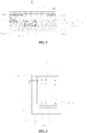
- FIG. 1 is a cross-sectional figure of FIG. 2 cutting along line A-B.
- the embodiment of the disclosure provides a circuit substrate 10.
- the circuit substrate 10 includes a non-display region 900.
- the non-display region 900 is provided with a first electrode layer 300 and a second electrode layer 100 on the first electrode layer 300.
- the contact area of the first electrode layer 300 contacting with the second electrode layer 100 at one side of the display region 800 is equal to that of the first electrode layer 300 contacting with the second electrode layer 100 at another side of the display region 800.
- the circuit substrate 10 further includes a first insulative layer 200 formed on a surface of the first electrode layer 300.
- the first insulative layer 200 is provided with two groove regions 210 at least on two sides of the display region 800 respectively.
- the shape of the groove regions 210 is not limited and may be a rectangle, an arc shape or the like.
- the groove regions 210 on the two sides of the display area 800 are symmetrical about a center line of the display region 800.
- the circuit substrate 10 further includes a second electrode layer 100 formed on the first insulative layer 200.
- the second electrode layer 100 covers at least a portion of the groove regions 210 and is in contact with the first electrode layer 300 exposed to the groove regions 210.
- the contact area of the first electrode layer contacting with the second electrode layer at one side of the display region is equal to that of the first electrode layer contacting with the second electrode layer at another side of the display region.
- the middle portion of the display device 20 is a display region 800, and the periphery of the display device is a non-display region 900.
- the non-display region 900 can be provided with a first electrode layer 300, a second electrode layer 100, and groove regions 210.
- the display region 800 can be formed into a rectangle.
- a width and depth of the groove regions 210 can be same or different in the entire non-display region 900, which is not limited herein. Taking the center line of the display region 800 as a symmetry axis, the widths and depths of the groove regions 210 located on the left and right sides of the display region 800 are the same.
- the width and depth of the groove regions 210 located on the upper and lower sides of the display region 800 can be different or same.
- the non-display region 900 can include a non-display region 900 located on the left and right sides of the display region 800 with respect to the center line of the display region 800.
- the contact area of the first electrode layer 300 contacting with the second electrode layer 100 at one side of the display region is equal to that of the first electrode layer 300 contacting with the second electrode layer 100 at an opposite side of the display region, which makes the resistance of the contact portion of the second electrode layer 100 contacting with the first electrode layer 300 at one side of the display region being equal to that of the first electrode layer 300 contacting with the second electrode layer 100 at an opposite side of the display region.
- the second electrode layer 100 can cover and fill only a part of the groove regions 210, or can fill and cover the entire groove regions 210, or cover and fill a part of the groove regions 210 and cover a part of the surface of the first insulative layer 200 or fill the entire groove regions 210 and cover the entire surface of the first insulative layer 200, as long as the widths of contact portions of the second electrode layer 100 contacting with the first electrode layer 300 in the non-display region 900 at one side of the display region 800 is ensured to be equal to that of the first electrode layer 300 contacting with the second electrode layer 100 in the non-display region at another side of the display region 800.
- the non-display region 900 of the circuit substrate 10 can be provided with an integrated chip for controlling the circuit substrate 10.
- the non-display region 900 may be provided with a gate driving module 50 and a source driving module 40.
- the gate driving module 50 can control ON and OFF state of the pixel switch in the display region 800.
- the source driving module 40 may provide a data signal to the pixel 625 located in the display region 800 after the pixel switch is switched on.
- a power supply wiring unit 810 can be further provided around the circuit substrate 10.
- the power supply wiring unit 810 can be used as a ground line.
- the power supply wiring unit 810 can be fixed to the circuit substrate 10 via the welding unit 820.
- the circuit substrate 10 further includes a base 700 on which the first electrode layer 300 is provided.
- the substrate 700 is used to support the circuit substrate 10.
- the base 700 is made of a hard material such as glass or plastic.
- the first electrode layer 300 is an electrical connection layer to switch a power supply signal.
- the first electrode layer 300 is made of ITO/Ag/ITO, and evaporated with the anode of the display region 800 to become a part of the anode.
- the functions of the two anodes are different.
- the anode located in the display region is used to control pixel emission of the display region, while the anode located in the non-display region only is used to switch the signal.
- the second electrode layer 100 becomes a part of a common cathode and can be formed by an evaporation process.
- the first electrode layer 300 and the second electrode layer 100 are in contact with each other, and the first electrode layer 300 is connected to the ground layer 500.
- the second electrode layer 100 is connected to the ground layer 500 via the first electrode layer 300.
- the first insulative layer 200 may be composed of silicon oxide, silicon nitride, or a combination of silicon oxide and silicon nitride.
- the groove regions 210 can be formed by means of photolithography or the like.
- the widths of the groove regions 210 of the non-display region 900 disposed on the sides of the display region 800 are equal.
- the equal width of the groove regions 210 facilitates the control of the process size of the second electrode layer 100 when the second electrode layer 100 is evaporated in the groove regions 210.
- the second electrode layer 100 covers the whole of the groove regions 210 and is in contact with the first electrode layer 300 exposed to the groove regions 210.
- the second electrode layer 100 covers the surface of the first insulative layer 200 and fills the groove regions 210.
- the widths of the groove regions 210 are equal on two sides of the display region 800.
- the contact areas of the first electrode layer 300 contacting with the second electrode layer 100 at one side of the display region is ensured to be equal to that of the first electrode layer 300 contacting with the second electrode layer 100 at an opposite side of the display region, without changing the evaporation process, and thus it is ensured that the currents flowing through the first electrode layer 300 and the second electrode layer 100 are the same.
- the second electrode layer 100 covers at least a portion of the surface of the first insulative layer 200 and at least a portion of the groove regions 210, and is in contacted with the first electrode layer 300 exposed to the groove regions 210. In one of the embodiments, the second electrode layer 100 covers all of the surface of the first insulative layer 200 and all of the groove regions 210, and is in contact with the first electrode layer 300 exposed to the first portion of the groove regions 210. On both sides of the display region 800, a high precision manufacturing process is required to provide the second electrode layer 100 covering only the groove regions 210, which increases the manufacturing cost.
- the second electrode layer 100 may be evaporated in a wider range of widths to cover the groove regions 210 and also to be formed on the surface of the first insulative layer 200, thereby reducing the difficulty of production and the production cost.
- the second electrode layer 100 covers a portion of the groove regions 210.
- the areas of the second electrode layer 100 covered by the second electrode layer 100 in the groove regions 210 are equal on both sides of the display region 800. Therefore, the resistances on both sides of the display region 800 are the same, and the currents flowing through are also the same on both sides, and the phenomenon of electrically shorted corner caused by the uneven current can be avoided.
- the width and depth of the groove regions 210 on the upper side of the display region 800 and the contact areas of the second electrode layer 100 contacting with the first electrode layer 300 are not limited. Instead, only the contact area of the second electrode layer 100 contacting with the first electrode layer 300 at one side of the display region 800 is required to be equal to that of the first electrode layer 300 contacting with the second electrode layer 100 at an opposite of the display region 800, so that the currents on the left and right sides of the screen body are ensured to be equal, which further ensures that the left and right sides of the screen body are not to be shorted.
- the contact areas of the second electrode layer 100 contacting with the first electrode layer 300 are equal on all sides of the display region 800, so that the currents on all sides of the screen body are ensured to be equal, which further ensures that all sides of the screen body are not to be shorted.
- the circuit substrate 10 further includes a circuit layer 600 and a ground layer 500 disposed on one side of the circuit layer 600.
- a second insulative layer 400 is formed on the upper surface of the circuit layer 600, and the first electrode layer 300 is formed on the upper surfaces of the second insulative layer 400 and the ground layer 500.
- the first electrode layer 300 is in contact with the ground layer 500.
- the circuit layer 600 can control the display of the screen.
- the second insulative layer 400 may function as a planarizing layer to planarize the surface of the circuit layer 600.
- the second insulative layer 400 may isolate the circuit layer 600 from the ground layer 500 to reach an insulation purpose.
- the second electrode layer 100, the first electrode layer 300 and the ground layer 500 are electrically connected to form a loop.
- the circuit layer 600 further includes a transistor switching element 620, a third insulative layer 611 and a fourth insulative layer 612.
- the transistor switching element includes a source 621, a drain 622 and a gate 623.
- a buffer layer 613 is disposed on the substrate 700, an active layer 624 is disposed on the buffer layer 613 and a fourth insulative layer 612 is disposed over the active layer 624.
- the gate 623 is evaporated on the fourth insulative layer 612, a third insulative layer 611 is disposed above the gate 623, and the source 621 and the drain 622 are disposed over the third insulative layer 611.
- the source 621 and the drain 622 are connected to the active layer 624 through the third insulative layer 611 and the fourth insulative layer 612 respectively.
- the second insulative layer 400 is located above the circuit layer 600 and covers the surface of the circuit layer 600 for planarizing the surface of the circuit layer 600.
- the circuit layer 600 may be formed with the ground layer 500 integrally, except that unnecessary portions of the ground layer 500 may be etched away during the process, leaving a portion for achieving conduction. Generally, the ground layer 500 is disposed on one side of the circuit layer 600.
- the third insulative layer 611 is configured to isolate the gate 623, the source 621 and the drain 622.
- the fourth insulative layer 612 is configured to isolate the active layer 624 and the gate 623.
- the gate 623 can be made of molybdenum.
- the second insulative layer 400 can be composed of silicon oxide, silicon nitride, or a combination of silicon oxide and silicon nitride.
- the first insulative layer 200 may also be composed of silicon oxide, silicon nitride, or a combination of silicon oxide and silicon nitride.
- the second electrode layer 100 is formed integrally with a cathode in the display region 800. In this way, the manufacturing process is reduced and the work efficiency is improved.
- the first electrode layer 300 is formed integrally with an anode in the display region 800. In this way, the manufacturing process is reduced and the work efficiency is improved.
- the first insulative layer 200 is formed integrally with a pixel defining layer in the display region 800. In this way, the manufacturing process is reduced and the work efficiency is improved.
- the second electrode layer 100 has a thickness of 0.1 mm to 0.2 mm.
- the second electrode layer 100 has the thickness on the surface of the first insulative layer 200 is same to that in the groove regions 210.
- the second electrode layer 100 with a thickness of 0.1 mm to 0.2 mm may have good electrical conductivity, as well as a reduced resistance, avoiding energy waste due to excessive heat caused by large resistance.
- a buffer layer 613 is further disposed between the active layer 624 and the substrate 700.
- the buffer layer 613 may isolate the substrate 700 from the active layer 624, and may also play a role of buffering.
- the embodiment of the disclosure further provides a display device.
- the display device includes a screen body, and further includes the circuit substrate 10.
- the circuit substrate 10 controls the screen to emit light.
- the second electrode layer 100 is electrically connected with the display region 800.
- the display region 800 is provided with a cathode and an anode that control the display of the pixel, and the second electrode layer 100 and the cathode may integrally form a common cathode.
- the currents flowing through both sides of the screen body are same due to the circuit substrate 10, and thus the phenomenon of electrically shorted corner caused by the uneven current on both sides of the screen body can be avoided. Therefore, the display device has a longer service life.
Landscapes
- Physics & Mathematics (AREA)
- Nonlinear Science (AREA)
- Engineering & Computer Science (AREA)
- Microelectronics & Electronic Packaging (AREA)
- Optics & Photonics (AREA)
- General Physics & Mathematics (AREA)
- Devices For Indicating Variable Information By Combining Individual Elements (AREA)
- Electroluminescent Light Sources (AREA)
Abstract
Description
- The present disclosure relates to the field of displaying, and more particularly, to a circuit substrate and a display device.
- For the conventional OLED display screen, during the producing process of a substrate, when a cathode layer is evaporated in the non-display region on both sides of the display region of the screen body, areas of contact portions of a cathode layer contacting with an electrode layer are not equal on both sides, which may easily cause an offset phenomenon. After the evaporated cathode layer is offset, the lapping areas of the evaporated cathode and the electrode layer are not equal on the left and right sides (two angles) of the display screen, and the resistance on both sides may be inconsistent. The inconsistency of the resistance may easily lead to a difference in current flow direction between the cathode and the electrode layer, resulting in different amounts of heat generated on both sides of the screen, and thus causing the phenomenon of electrically shorted corner of the screen body.
- Based on the above, regarding the problem of electrically shorted corner caused by the inconsistency of the lapping resistance of a cathode and an electrode layer on both sides (two corners) of the display screen body, there is a need to provide a circuit substrate and a display device with same resistance on both sides of the display screen body.
- A circuit substrate is provided, including a display region and a non-display region, the non-display region including:
- a first electrode layer, and
- a second electrode layer located on the first electrode layer. A contact area of the first electrode layer contacting with the second electrode layer at one side of the display region is equal to that of the first electrode layer contacting with the second electrode layer at another side of the display region.
- In this embodiment, the contact area of the first electrode layer contacting with the second electrode layer at one side of the display region is equal to that of the first electrode layer contacting with the second electrode layer at another side of the display region, so that the first electrode layer and the second electrode layer have same contact resistance, and therefore the currents flowing through both sides of the display region are the same, and the phenomenon of electrically shorted corner can be avoided.
- In one of the embodiments, the circuit substrate further includes a first insulative layer formed on the first electrode layer, the first insulative layer being provided with two groove regions at least on two sides of the display region. The second electrode layer covers at least a portion of the groove regions and is in contact with the first electrode layer exposed to the groove regions, and the contact area of the first electrode layer contacting with the second electrode layer at one side of the display region is equal to that of the first electrode layer contacting with the second electrode layer at another side of the display region.
- In this embodiment, the groove regions are configured to make the second electrode layer contact with the first electrode layer.
- In one of the embodiments, the two groove regions on both sides of the display region are symmetrical about a center line of the display region.
- In one of the embodiments, the two groove regions on both sides of the display region have equal widths.
- In one of the embodiments, the second electrode layer covers the whole of the groove regions and is in contact with the first electrode layer exposed to the groove regions.
- In this embodiment, the groove regions are in an equal width, which makes the width of the second electrode layer in contact with the first electrode layer to be the same on both sides after the second electrode layer covers all of the groove regions, and the same resistance can be ensured on both sides of the display region.
- In one of the embodiments, the second electrode layer covers at least a portion of a surface of the first insulative layer and at least a portion of the groove regions, and is in contact with the first electrode layer exposed to the groove regions.
- In one of the embodiments, the second electrode layer covers the whole surface of the first insulative layer and of the whole of the groove regions, and is in contact with the first electrode layer exposed to the groove regions.
- In this embodiment, covering the evaporated area of the second electrode layer with the area of the groove regions may reduce the process difficulty of evaporating the second electrode layer, while the requirement that the contact portions of the second electrode layer contacting with the first electrode layer have equal widths on both sides can be satisfied, and the same resistance on both sides of the display region can be ensured.
- In one of the embodiments, the circuit board further includes: a circuit layer, and a ground layer disposed on a side of the circuit layer. A second insulative layer is formed on an upper surface of the circuit layer, and the first insulative layer is formed on upper surfaces of the second insulative layer and the ground layer, and the first electrode layer is in contact with the ground layer.
- In this embodiment, the first electrode layer is in contact with the ground layer, which makes the second electrode layer to be conducted with the ground layer through the first electrode layer, so as to achieve signal switching.
- In one of the embodiments, the second electrode layer is formed integrally with a cathode in the display region.
- In this embodiment, the second electrode layer is formed integrally with a cathode in the display region, which may reduce the production process and improve work efficiency.
- In one of the embodiments, the first insulative layer is formed integrally with a pixel defining layer provided in the display region.
- In this embodiment, the first insulative layer is formed integrally with a pixel defining layer in the display region, which may reduce the production process and improve work efficiency.
- In one of the embodiments, the second electrode layer has a thickness of 0.1mm-0.2mm.
- In this embodiment, the second electrode layer with a thickness of 0.1 mm to 0.2 mm may have good electrical conductivity, as well as a reduced resistance, avoiding energy waste due to excessive heat caused by large resistance.
- A display device is also provided, including a screen body. The display device further includes the circuit substrate that controls the screen body to emit light.
- In this embodiment, the circuit substrate may cause the currents flowing through both sides of the display region of the screen body to be the same, and the phenomenon of electrically shorted corner caused by the uneven currents on both sides of the display region of the screen body can be avoided. Therefore, the display device has a longer service life.
-
-
FIG. 1 is a schematic cross-sectional diagram of a circuit substrate according to an embodiment of the present disclosure. -
FIG. 2 is a structural diagram of a display device according to an embodiment of the present disclosure. -
- 10: Circuit Substrate;
- 100: Second Electrode Layer;
- 200: Insulative Layer;
- 300: First Electrode Layer;
- 210: Groove Region;
- 400: Second Insulative Layer;
- 500: Ground Layer;
- 600: Circuit Layer;
- 611: Third Insulative Layer;
- 612: Fourth Insulative Layer;
- 613: Buffer Layer;
- 620: Transistor Switching Element;
- 700: Substrate;
- 621: Source;
- 622: Drain;
- 623: Gate;
- 624: Active Layer;
- 625: Pixel;
- 40: Source Driving Module;
- 50: Gate Driving Module;
- 20: Display Device;
- 800: Display Region;
- 810: Power Supply Wiring Unit;
- 820: Welding Unit;
- 900: Non-Display Region.
- In order to make the purpose, technical scheme and technical effect of the disclosure more clear, the specific embodiments of the present disclosure are described below with reference to the accompanying drawings. It is to be understood that the specific embodiments described herein are merely used to illustrate the disclosure and are not intended to limit the disclosure.
- Referring to
FIGS. 1-2, FIG. 1 is a cross-sectional figure ofFIG. 2 cutting along line A-B. The embodiment of the disclosure provides acircuit substrate 10. Thecircuit substrate 10 includes anon-display region 900. Thenon-display region 900 is provided with afirst electrode layer 300 and asecond electrode layer 100 on thefirst electrode layer 300. The contact area of thefirst electrode layer 300 contacting with thesecond electrode layer 100 at one side of thedisplay region 800 is equal to that of thefirst electrode layer 300 contacting with thesecond electrode layer 100 at another side of thedisplay region 800. - Preferably, the
circuit substrate 10 further includes afirst insulative layer 200 formed on a surface of thefirst electrode layer 300. Thefirst insulative layer 200 is provided with twogroove regions 210 at least on two sides of thedisplay region 800 respectively. It can be understood that the shape of thegroove regions 210 is not limited and may be a rectangle, an arc shape or the like. Preferably, thegroove regions 210 on the two sides of thedisplay area 800 are symmetrical about a center line of thedisplay region 800. Thecircuit substrate 10 further includes asecond electrode layer 100 formed on thefirst insulative layer 200. Thesecond electrode layer 100 covers at least a portion of thegroove regions 210 and is in contact with thefirst electrode layer 300 exposed to thegroove regions 210. The contact area of the first electrode layer contacting with the second electrode layer at one side of the display region is equal to that of the first electrode layer contacting with the second electrode layer at another side of the display region. - The middle portion of the
display device 20 is adisplay region 800, and the periphery of the display device is anon-display region 900. Thenon-display region 900 can be provided with afirst electrode layer 300, asecond electrode layer 100, andgroove regions 210. In one embodiment, thedisplay region 800 can be formed into a rectangle. A width and depth of thegroove regions 210 can be same or different in the entirenon-display region 900, which is not limited herein. Taking the center line of thedisplay region 800 as a symmetry axis, the widths and depths of thegroove regions 210 located on the left and right sides of thedisplay region 800 are the same. The width and depth of thegroove regions 210 located on the upper and lower sides of thedisplay region 800 can be different or same. - It can be understood that the
non-display region 900 can include anon-display region 900 located on the left and right sides of thedisplay region 800 with respect to the center line of thedisplay region 800. In thenon-display region 900 on the left and right sides of thedisplay region 800, the contact area of thefirst electrode layer 300 contacting with thesecond electrode layer 100 at one side of the display region is equal to that of thefirst electrode layer 300 contacting with thesecond electrode layer 100 at an opposite side of the display region, which makes the resistance of the contact portion of thesecond electrode layer 100 contacting with thefirst electrode layer 300 at one side of the display region being equal to that of thefirst electrode layer 300 contacting with thesecond electrode layer 100 at an opposite side of the display region. Therefore, the current flowing through thefirst electrode layer 300 and the current flowing through thesecond electrode layer 100 are same, and as a result, a phenomenon of electrically shorted corner due to different currents flowing through two sides of thedisplay region 800 can be avoided. Thesecond electrode layer 100 can cover and fill only a part of thegroove regions 210, or can fill and cover theentire groove regions 210, or cover and fill a part of thegroove regions 210 and cover a part of the surface of thefirst insulative layer 200 or fill theentire groove regions 210 and cover the entire surface of thefirst insulative layer 200, as long as the widths of contact portions of thesecond electrode layer 100 contacting with thefirst electrode layer 300 in thenon-display region 900 at one side of thedisplay region 800 is ensured to be equal to that of thefirst electrode layer 300 contacting with thesecond electrode layer 100 in the non-display region at another side of thedisplay region 800. - In one of the embodiments, the
non-display region 900 of thecircuit substrate 10 can be provided with an integrated chip for controlling thecircuit substrate 10. Thenon-display region 900 may be provided with agate driving module 50 and asource driving module 40. Thegate driving module 50 can control ON and OFF state of the pixel switch in thedisplay region 800. Thesource driving module 40 may provide a data signal to thepixel 625 located in thedisplay region 800 after the pixel switch is switched on. A powersupply wiring unit 810 can be further provided around thecircuit substrate 10. The powersupply wiring unit 810 can be used as a ground line. The powersupply wiring unit 810 can be fixed to thecircuit substrate 10 via thewelding unit 820. - The
circuit substrate 10 further includes a base 700 on which thefirst electrode layer 300 is provided. Thesubstrate 700 is used to support thecircuit substrate 10. Thebase 700 is made of a hard material such as glass or plastic. Thefirst electrode layer 300 is an electrical connection layer to switch a power supply signal. Thefirst electrode layer 300 is made of ITO/Ag/ITO, and evaporated with the anode of thedisplay region 800 to become a part of the anode. The functions of the two anodes are different. The anode located in the display region is used to control pixel emission of the display region, while the anode located in the non-display region only is used to switch the signal. Thesecond electrode layer 100 becomes a part of a common cathode and can be formed by an evaporation process. Thefirst electrode layer 300 and thesecond electrode layer 100 are in contact with each other, and thefirst electrode layer 300 is connected to theground layer 500. Thesecond electrode layer 100 is connected to theground layer 500 via thefirst electrode layer 300. Thefirst insulative layer 200 may be composed of silicon oxide, silicon nitride, or a combination of silicon oxide and silicon nitride. Thegroove regions 210 can be formed by means of photolithography or the like. - In one of the embodiments, the widths of the
groove regions 210 of thenon-display region 900 disposed on the sides of thedisplay region 800 are equal. The equal width of thegroove regions 210 facilitates the control of the process size of thesecond electrode layer 100 when thesecond electrode layer 100 is evaporated in thegroove regions 210. - In one of the embodiments, the
second electrode layer 100 covers the whole of thegroove regions 210 and is in contact with thefirst electrode layer 300 exposed to thegroove regions 210. In the manufacturing process of thecircuit substrate 10, when thesecond electrode layer 100 is evaporated, thesecond electrode layer 100 covers the surface of thefirst insulative layer 200 and fills thegroove regions 210. The widths of thegroove regions 210 are equal on two sides of thedisplay region 800. Therefore, through thegroove regions 210, the contact areas of thefirst electrode layer 300 contacting with thesecond electrode layer 100 at one side of the display region is ensured to be equal to that of thefirst electrode layer 300 contacting with thesecond electrode layer 100 at an opposite side of the display region, without changing the evaporation process, and thus it is ensured that the currents flowing through thefirst electrode layer 300 and thesecond electrode layer 100 are the same. - In one of the embodiments, the
second electrode layer 100 covers at least a portion of the surface of thefirst insulative layer 200 and at least a portion of thegroove regions 210, and is in contacted with thefirst electrode layer 300 exposed to thegroove regions 210. In one of the embodiments, thesecond electrode layer 100 covers all of the surface of thefirst insulative layer 200 and all of thegroove regions 210, and is in contact with thefirst electrode layer 300 exposed to the first portion of thegroove regions 210. On both sides of thedisplay region 800, a high precision manufacturing process is required to provide thesecond electrode layer 100 covering only thegroove regions 210, which increases the manufacturing cost. Thus, in the process of producing thesecond electrode layer 100, thesecond electrode layer 100 may be evaporated in a wider range of widths to cover thegroove regions 210 and also to be formed on the surface of thefirst insulative layer 200, thereby reducing the difficulty of production and the production cost. - In one of the embodiments, the
second electrode layer 100 covers a portion of thegroove regions 210. The areas of thesecond electrode layer 100 covered by thesecond electrode layer 100 in thegroove regions 210 are equal on both sides of thedisplay region 800. Therefore, the resistances on both sides of thedisplay region 800 are the same, and the currents flowing through are also the same on both sides, and the phenomenon of electrically shorted corner caused by the uneven current can be avoided. - In this embodiment, the width and depth of the
groove regions 210 on the upper side of thedisplay region 800 and the contact areas of thesecond electrode layer 100 contacting with thefirst electrode layer 300 are not limited. Instead, only the contact area of thesecond electrode layer 100 contacting with thefirst electrode layer 300 at one side of thedisplay region 800 is required to be equal to that of thefirst electrode layer 300 contacting with thesecond electrode layer 100 at an opposite of thedisplay region 800, so that the currents on the left and right sides of the screen body are ensured to be equal, which further ensures that the left and right sides of the screen body are not to be shorted. In another embodiment, the contact areas of thesecond electrode layer 100 contacting with thefirst electrode layer 300 are equal on all sides of thedisplay region 800, so that the currents on all sides of the screen body are ensured to be equal, which further ensures that all sides of the screen body are not to be shorted. - In one of the embodiments, the
circuit substrate 10 further includes acircuit layer 600 and aground layer 500 disposed on one side of thecircuit layer 600. Asecond insulative layer 400 is formed on the upper surface of thecircuit layer 600, and thefirst electrode layer 300 is formed on the upper surfaces of thesecond insulative layer 400 and theground layer 500. Thefirst electrode layer 300 is in contact with theground layer 500. Thecircuit layer 600 can control the display of the screen. Thesecond insulative layer 400 may function as a planarizing layer to planarize the surface of thecircuit layer 600. Thesecond insulative layer 400 may isolate thecircuit layer 600 from theground layer 500 to reach an insulation purpose. Thesecond electrode layer 100, thefirst electrode layer 300 and theground layer 500 are electrically connected to form a loop. - In one of the embodiments, the
circuit layer 600 further includes atransistor switching element 620, athird insulative layer 611 and afourth insulative layer 612. The transistor switching element includes asource 621, adrain 622 and agate 623. Abuffer layer 613 is disposed on thesubstrate 700, anactive layer 624 is disposed on thebuffer layer 613 and afourth insulative layer 612 is disposed over theactive layer 624. Thegate 623 is evaporated on thefourth insulative layer 612, athird insulative layer 611 is disposed above thegate 623, and thesource 621 and thedrain 622 are disposed over thethird insulative layer 611. Thesource 621 and thedrain 622 are connected to theactive layer 624 through thethird insulative layer 611 and thefourth insulative layer 612 respectively. Thesecond insulative layer 400 is located above thecircuit layer 600 and covers the surface of thecircuit layer 600 for planarizing the surface of thecircuit layer 600. Thecircuit layer 600 may be formed with theground layer 500 integrally, except that unnecessary portions of theground layer 500 may be etched away during the process, leaving a portion for achieving conduction. Generally, theground layer 500 is disposed on one side of thecircuit layer 600. Thethird insulative layer 611 is configured to isolate thegate 623, thesource 621 and thedrain 622. Thefourth insulative layer 612 is configured to isolate theactive layer 624 and thegate 623. Preferably, thegate 623 can be made of molybdenum. Thesecond insulative layer 400 can be composed of silicon oxide, silicon nitride, or a combination of silicon oxide and silicon nitride. Thefirst insulative layer 200 may also be composed of silicon oxide, silicon nitride, or a combination of silicon oxide and silicon nitride. After thegate 623 is triggered by a voltage, thesource 621 and thedrain 622 may be turned on. After thesource 621 and thedrain 622 are turned on, thetransistor switching element 620 is controlled to be switched on. - In one of the embodiments, the
second electrode layer 100 is formed integrally with a cathode in thedisplay region 800. In this way, the manufacturing process is reduced and the work efficiency is improved. - In one of the embodiments, the
first electrode layer 300 is formed integrally with an anode in thedisplay region 800. In this way, the manufacturing process is reduced and the work efficiency is improved. - In one of the embodiments, the
first insulative layer 200 is formed integrally with a pixel defining layer in thedisplay region 800. In this way, the manufacturing process is reduced and the work efficiency is improved. - In one of the embodiments, the
second electrode layer 100 has a thickness of 0.1 mm to 0.2 mm. Preferably, thesecond electrode layer 100 has the thickness on the surface of thefirst insulative layer 200 is same to that in thegroove regions 210. Thesecond electrode layer 100 with a thickness of 0.1 mm to 0.2 mm may have good electrical conductivity, as well as a reduced resistance, avoiding energy waste due to excessive heat caused by large resistance. - In one of the embodiments, a
buffer layer 613 is further disposed between theactive layer 624 and thesubstrate 700. Thebuffer layer 613 may isolate thesubstrate 700 from theactive layer 624, and may also play a role of buffering. - The embodiment of the disclosure further provides a display device. The display device includes a screen body, and further includes the
circuit substrate 10. Thecircuit substrate 10 controls the screen to emit light. Thesecond electrode layer 100 is electrically connected with thedisplay region 800. Thedisplay region 800 is provided with a cathode and an anode that control the display of the pixel, and thesecond electrode layer 100 and the cathode may integrally form a common cathode. The currents flowing through both sides of the screen body are same due to thecircuit substrate 10, and thus the phenomenon of electrically shorted corner caused by the uneven current on both sides of the screen body can be avoided. Therefore, the display device has a longer service life. - When a feature or element is herein referred to as being "on" another feature or element, it can be directly on the other feature or element or intervening features and/or elements may also be present. It will also be understood that, when a feature or element is referred to as being "connected", "attached" or "coupled" to another feature or element, it can be directly connected, attached or coupled to the other feature or element or intervening features or elements may be present. In contrast, when a feature or element is referred to as being "directly on" another feature or element, there are no intervening features or elements present. The terms "vertical", "horizontal", "left", "right" or the like, as used herein, are for illustrative purposes only.
- The above are embodiments of the disclosure described in detail, and should not be deemed as limitations to the scope of the present disclosure. It should be noted that variations and improvements will become apparent to those skilled in the art to which the present disclosure pertains without departing from its spirit and scope. Therefore, the scope of the present disclosure is defined by the appended claims.
Claims (12)
- A circuit substrate, comprising:a display region (800),anda non-display region (900) including:a first electrode layer (300), anda second electrode layer (100)located on the first electrode layer (300),wherein a contact area of the first electrode layer (300) contacting with the second electrode layer (100) at one side of the display region (800) is equal to that of the first electrode layer (300) contacting with the second electrode layer (100) at another side of the display region (800).
- The circuit substrate of claim 1, further comprising a first insulative layer (200) formed on the first electrode layer (300), the first insulative layer (200) being provided with two groove regions (210) at least on two sides of the display region (800), wherein the second electrode layer (100) covers at least a portion of the groove regions (210) and is in contact with the first electrode layer (300) exposed to the groove regions (210), and a contact area of the first electrode layer (300) contacting with the second electrode layer (100) at one side of the display region (800) is equal to that of the first electrode layer (300) contacting with the second electrode layer (100) at another side of the display region (800).
- The circuit substrate of claim 2, wherein the two groove regions (210) on both sides of the display region (800) are symmetrical about a center line of the display region (800).
- The circuit substrate of claim 2, wherein the two groove regions (210) on both sides of the display region (800) have equal widths.
- The circuit substrate of claim 2, wherein the second electrode layer (100) covers the whole of the groove regions (210) and is in contact with the first electrode layer (300) exposed to the groove regions (210).
- The circuit substrate of claim 2, wherein the second electrode layer (100) covers at least a portion of a surface of the first insulative layer (200) and at least a portion of the groove regions (210), and is in contact with the first electrode layer (300) exposed to the groove regions (210).
- The circuit substrate of claim 6, wherein the second electrode layer (100) covers the whole surface of the first insulative layer (200) and the whole of the groove regions (210), and is in contact with the first electrode layer (300) exposed to the groove regions (210).
- The circuit substrate of any one of claims 1 to 7, further comprising a circuit layer (600), and a ground layer (500) disposed on a side of the circuit layer (600), wherein a second insulative layer (400) is formed on an upper surface of the circuit layer (600), and the first insulative layer (300) is formed on upper surfaces of the second insulative layer(400) and the ground layer (500),and the first electrode layer (300) is in contact with the ground layer (500).
- The circuit substrate of claim 1, wherein the second electrode layer (100) is formed integrally with a cathode in the display region (800).
- The circuit substrate of claim 1, wherein the first insulative layer (200) is formed integrally with a pixel defining layer provided in the display region (800).
- The circuit substrate of claim 1, wherein the second electrode layer (100) has a thickness of 0.1mm-0.2mm.
- A display device, comprising a screen body, wherein the display device further comprises the circuit substrate of any one of claims 1 to 11, and the circuit substrate controls the screen body to emit light.
Applications Claiming Priority (2)
| Application Number | Priority Date | Filing Date | Title |
|---|---|---|---|
| CN201710518353.4A CN109216403A (en) | 2017-06-29 | 2017-06-29 | Circuit substrate and display device |
| PCT/CN2018/084520 WO2019001122A1 (en) | 2017-06-29 | 2018-04-25 | Circuit board and display device |
Publications (2)
| Publication Number | Publication Date |
|---|---|
| EP3567633A1 true EP3567633A1 (en) | 2019-11-13 |
| EP3567633A4 EP3567633A4 (en) | 2020-08-12 |
Family
ID=63960361
Family Applications (1)
| Application Number | Title | Priority Date | Filing Date |
|---|---|---|---|
| EP18824991.6A Pending EP3567633A4 (en) | 2017-06-29 | 2018-04-25 | CIRCUIT BOARD AND DISPLAY DEVICE |
Country Status (7)
| Country | Link |
|---|---|
| US (1) | US20200111863A1 (en) |
| EP (1) | EP3567633A4 (en) |
| JP (1) | JP2020506431A (en) |
| KR (1) | KR20190099332A (en) |
| CN (1) | CN109216403A (en) |
| TW (1) | TWI665504B (en) |
| WO (1) | WO2019001122A1 (en) |
Families Citing this family (1)
| Publication number | Priority date | Publication date | Assignee | Title |
|---|---|---|---|---|
| WO2024123812A1 (en) | 2022-12-05 | 2024-06-13 | Shattuck Labs, Inc. | Fusion proteins for the treatment of cardiometabolic diseases |
Family Cites Families (11)
| Publication number | Priority date | Publication date | Assignee | Title |
|---|---|---|---|---|
| JP2001102169A (en) * | 1999-10-01 | 2001-04-13 | Sanyo Electric Co Ltd | EL display device |
| KR100611153B1 (en) * | 2003-11-27 | 2006-08-09 | 삼성에스디아이 주식회사 | Flat panel display elements |
| KR100581903B1 (en) * | 2004-03-09 | 2006-05-22 | 삼성에스디아이 주식회사 | Electroluminescent display device |
| US7839083B2 (en) * | 2007-02-08 | 2010-11-23 | Seiko Epson Corporation | Light emitting device and electronic apparatus |
| KR101415684B1 (en) * | 2011-07-07 | 2014-08-07 | 엘지디스플레이 주식회사 | Substrate for organic electro luminescent device and method of fabricating the same |
| US20130056784A1 (en) * | 2011-09-02 | 2013-03-07 | Lg Display Co., Ltd. | Organic Light-Emitting Display Device and Method of Fabricating the Same |
| KR101521676B1 (en) * | 2011-09-20 | 2015-05-19 | 엘지디스플레이 주식회사 | Organic light emitting diode display and method for manufacturing the same |
| KR20150006125A (en) * | 2013-07-08 | 2015-01-16 | 삼성디스플레이 주식회사 | Organic light emitting display devices and methods of manufacturing organic light emitting display devices |
| JP6440486B2 (en) * | 2014-12-19 | 2018-12-19 | 株式会社ジャパンディスプレイ | LCD panel |
| KR102404930B1 (en) * | 2014-12-24 | 2022-06-08 | 삼성디스플레이 주식회사 | Window for display device and display device comprising the same |
| CN207265055U (en) * | 2017-06-29 | 2018-04-20 | 昆山国显光电有限公司 | Circuit substrate and display device |
-
2017
- 2017-06-29 CN CN201710518353.4A patent/CN109216403A/en active Pending
-
2018
- 2018-04-25 WO PCT/CN2018/084520 patent/WO2019001122A1/en not_active Ceased
- 2018-04-25 JP JP2019541797A patent/JP2020506431A/en active Pending
- 2018-04-25 EP EP18824991.6A patent/EP3567633A4/en active Pending
- 2018-04-25 KR KR1020197023052A patent/KR20190099332A/en not_active Ceased
- 2018-04-25 US US16/326,913 patent/US20200111863A1/en not_active Abandoned
- 2018-05-04 TW TW107115161A patent/TWI665504B/en active
Also Published As
| Publication number | Publication date |
|---|---|
| TW201827909A (en) | 2018-08-01 |
| JP2020506431A (en) | 2020-02-27 |
| TWI665504B (en) | 2019-07-11 |
| CN109216403A (en) | 2019-01-15 |
| US20200111863A1 (en) | 2020-04-09 |
| WO2019001122A1 (en) | 2019-01-03 |
| EP3567633A4 (en) | 2020-08-12 |
| KR20190099332A (en) | 2019-08-26 |
Similar Documents
| Publication | Publication Date | Title |
|---|---|---|
| CN114361226A (en) | Display panel and method of making the same | |
| KR100963075B1 (en) | Organic light emitting display device | |
| CN101409304B (en) | Organic el display device | |
| KR102454728B1 (en) | Organic light emitting display device | |
| CN112289945B (en) | Display panel and manufacturing method thereof | |
| TWI668855B (en) | Micro LED display panel | |
| JP2004087682A (en) | Thin film transistor, image display device and image display device | |
| CN110783490A (en) | Display panel and preparation method thereof | |
| KR101871420B1 (en) | Organic Light Emitting Display device | |
| JP2007288181A (en) | Amorphous silicon thin film transistor and organic light emitting display comprising the same | |
| JP2000242196A (en) | Electroluminescence display device | |
| US11569332B2 (en) | Display substrate and display device | |
| US7038240B2 (en) | Color display device | |
| JP2021108366A (en) | Thin film device | |
| CN112635693A (en) | Array substrate and preparation method thereof | |
| EP3605641A1 (en) | Pixel cell, display substrate, and display panel | |
| CN114005855B (en) | Array substrate, display panel and panel dead pixel repairing method | |
| KR101734920B1 (en) | Organic electroluminescent device and Method of fabricating the same | |
| US20200111863A1 (en) | Circuit board and display device | |
| US10431689B2 (en) | Thin film transistor and display device | |
| KR100698678B1 (en) | Light emitting display device and manufacturing method thereof | |
| US7164399B2 (en) | Display device | |
| CN207265055U (en) | Circuit substrate and display device | |
| US20140125903A1 (en) | Liquid crystal display device | |
| CN111129035A (en) | Array substrate, display panel and display device |
Legal Events
| Date | Code | Title | Description |
|---|---|---|---|
| STAA | Information on the status of an ep patent application or granted ep patent |
Free format text: STATUS: THE INTERNATIONAL PUBLICATION HAS BEEN MADE |
|
| PUAI | Public reference made under article 153(3) epc to a published international application that has entered the european phase |
Free format text: ORIGINAL CODE: 0009012 |
|
| STAA | Information on the status of an ep patent application or granted ep patent |
Free format text: STATUS: REQUEST FOR EXAMINATION WAS MADE |
|
| 17P | Request for examination filed |
Effective date: 20190807 |
|
| AK | Designated contracting states |
Kind code of ref document: A1 Designated state(s): AL AT BE BG CH CY CZ DE DK EE ES FI FR GB GR HR HU IE IS IT LI LT LU LV MC MK MT NL NO PL PT RO RS SE SI SK SM TR |
|
| AX | Request for extension of the european patent |
Extension state: BA ME |
|
| A4 | Supplementary search report drawn up and despatched |
Effective date: 20200710 |
|
| RIC1 | Information provided on ipc code assigned before grant |
Ipc: H01L 51/52 20060101ALI20200706BHEP Ipc: G02F 1/155 20060101ALI20200706BHEP Ipc: H01L 51/50 20060101ALI20200706BHEP Ipc: H01L 27/32 20060101AFI20200706BHEP |
|
| DAV | Request for validation of the european patent (deleted) | ||
| DAX | Request for extension of the european patent (deleted) | ||
| STAA | Information on the status of an ep patent application or granted ep patent |
Free format text: STATUS: EXAMINATION IS IN PROGRESS |
|
| 17Q | First examination report despatched |
Effective date: 20221208 |