EP3564756A1 - Electrophotographic photoreceptor and image forming apparatus - Google Patents
Electrophotographic photoreceptor and image forming apparatus Download PDFInfo
- Publication number
- EP3564756A1 EP3564756A1 EP17887216.4A EP17887216A EP3564756A1 EP 3564756 A1 EP3564756 A1 EP 3564756A1 EP 17887216 A EP17887216 A EP 17887216A EP 3564756 A1 EP3564756 A1 EP 3564756A1
- Authority
- EP
- European Patent Office
- Prior art keywords
- electrophotographic photoreceptor
- layer
- substrate
- cylindrical
- roughness
- Prior art date
- Legal status (The legal status is an assumption and is not a legal conclusion. Google has not performed a legal analysis and makes no representation as to the accuracy of the status listed.)
- Granted
Links
Images






Classifications
-
- G—PHYSICS
- G03—PHOTOGRAPHY; CINEMATOGRAPHY; ANALOGOUS TECHNIQUES USING WAVES OTHER THAN OPTICAL WAVES; ELECTROGRAPHY; HOLOGRAPHY
- G03G—ELECTROGRAPHY; ELECTROPHOTOGRAPHY; MAGNETOGRAPHY
- G03G5/00—Recording-members for original recording by exposure, e.g. to light, to heat or to electrons; Manufacture thereof; Selection of materials therefor
- G03G5/02—Charge-receiving layers
- G03G5/04—Photoconductive layers; Charge-generation layers or charge-transporting layers; Additives therefor; Binders therefor
- G03G5/08—Photoconductive layers; Charge-generation layers or charge-transporting layers; Additives therefor; Binders therefor characterised by the photoconductive material being inorganic
- G03G5/082—Photoconductive layers; Charge-generation layers or charge-transporting layers; Additives therefor; Binders therefor characterised by the photoconductive material being inorganic and not being incorporated in a bonding material, e.g. vacuum deposited
- G03G5/08214—Silicon-based
-
- G—PHYSICS
- G03—PHOTOGRAPHY; CINEMATOGRAPHY; ANALOGOUS TECHNIQUES USING WAVES OTHER THAN OPTICAL WAVES; ELECTROGRAPHY; HOLOGRAPHY
- G03G—ELECTROGRAPHY; ELECTROPHOTOGRAPHY; MAGNETOGRAPHY
- G03G5/00—Recording-members for original recording by exposure, e.g. to light, to heat or to electrons; Manufacture thereof; Selection of materials therefor
- G03G5/14—Inert intermediate or cover layers for charge-receiving layers
- G03G5/147—Cover layers
- G03G5/14708—Cover layers comprising organic material
-
- G—PHYSICS
- G03—PHOTOGRAPHY; CINEMATOGRAPHY; ANALOGOUS TECHNIQUES USING WAVES OTHER THAN OPTICAL WAVES; ELECTROGRAPHY; HOLOGRAPHY
- G03G—ELECTROGRAPHY; ELECTROPHOTOGRAPHY; MAGNETOGRAPHY
- G03G15/00—Apparatus for electrographic processes using a charge pattern
- G03G15/75—Details relating to xerographic drum, band or plate, e.g. replacing, testing
- G03G15/751—Details relating to xerographic drum, band or plate, e.g. replacing, testing relating to drum
-
- G—PHYSICS
- G03—PHOTOGRAPHY; CINEMATOGRAPHY; ANALOGOUS TECHNIQUES USING WAVES OTHER THAN OPTICAL WAVES; ELECTROGRAPHY; HOLOGRAPHY
- G03G—ELECTROGRAPHY; ELECTROPHOTOGRAPHY; MAGNETOGRAPHY
- G03G5/00—Recording-members for original recording by exposure, e.g. to light, to heat or to electrons; Manufacture thereof; Selection of materials therefor
- G03G5/02—Charge-receiving layers
- G03G5/04—Photoconductive layers; Charge-generation layers or charge-transporting layers; Additives therefor; Binders therefor
- G03G5/08—Photoconductive layers; Charge-generation layers or charge-transporting layers; Additives therefor; Binders therefor characterised by the photoconductive material being inorganic
-
- G—PHYSICS
- G03—PHOTOGRAPHY; CINEMATOGRAPHY; ANALOGOUS TECHNIQUES USING WAVES OTHER THAN OPTICAL WAVES; ELECTROGRAPHY; HOLOGRAPHY
- G03G—ELECTROGRAPHY; ELECTROPHOTOGRAPHY; MAGNETOGRAPHY
- G03G5/00—Recording-members for original recording by exposure, e.g. to light, to heat or to electrons; Manufacture thereof; Selection of materials therefor
- G03G5/02—Charge-receiving layers
- G03G5/04—Photoconductive layers; Charge-generation layers or charge-transporting layers; Additives therefor; Binders therefor
- G03G5/08—Photoconductive layers; Charge-generation layers or charge-transporting layers; Additives therefor; Binders therefor characterised by the photoconductive material being inorganic
- G03G5/082—Photoconductive layers; Charge-generation layers or charge-transporting layers; Additives therefor; Binders therefor characterised by the photoconductive material being inorganic and not being incorporated in a bonding material, e.g. vacuum deposited
- G03G5/08214—Silicon-based
- G03G5/08221—Silicon-based comprising one or two silicon based layers
-
- G—PHYSICS
- G03—PHOTOGRAPHY; CINEMATOGRAPHY; ANALOGOUS TECHNIQUES USING WAVES OTHER THAN OPTICAL WAVES; ELECTROGRAPHY; HOLOGRAPHY
- G03G—ELECTROGRAPHY; ELECTROPHOTOGRAPHY; MAGNETOGRAPHY
- G03G5/00—Recording-members for original recording by exposure, e.g. to light, to heat or to electrons; Manufacture thereof; Selection of materials therefor
- G03G5/02—Charge-receiving layers
- G03G5/04—Photoconductive layers; Charge-generation layers or charge-transporting layers; Additives therefor; Binders therefor
- G03G5/08—Photoconductive layers; Charge-generation layers or charge-transporting layers; Additives therefor; Binders therefor characterised by the photoconductive material being inorganic
- G03G5/082—Photoconductive layers; Charge-generation layers or charge-transporting layers; Additives therefor; Binders therefor characterised by the photoconductive material being inorganic and not being incorporated in a bonding material, e.g. vacuum deposited
- G03G5/08214—Silicon-based
- G03G5/08235—Silicon-based comprising three or four silicon-based layers
-
- G—PHYSICS
- G03—PHOTOGRAPHY; CINEMATOGRAPHY; ANALOGOUS TECHNIQUES USING WAVES OTHER THAN OPTICAL WAVES; ELECTROGRAPHY; HOLOGRAPHY
- G03G—ELECTROGRAPHY; ELECTROPHOTOGRAPHY; MAGNETOGRAPHY
- G03G5/00—Recording-members for original recording by exposure, e.g. to light, to heat or to electrons; Manufacture thereof; Selection of materials therefor
- G03G5/10—Bases for charge-receiving or other layers
-
- G—PHYSICS
- G03—PHOTOGRAPHY; CINEMATOGRAPHY; ANALOGOUS TECHNIQUES USING WAVES OTHER THAN OPTICAL WAVES; ELECTROGRAPHY; HOLOGRAPHY
- G03G—ELECTROGRAPHY; ELECTROPHOTOGRAPHY; MAGNETOGRAPHY
- G03G5/00—Recording-members for original recording by exposure, e.g. to light, to heat or to electrons; Manufacture thereof; Selection of materials therefor
- G03G5/10—Bases for charge-receiving or other layers
- G03G5/102—Bases for charge-receiving or other layers consisting of or comprising metals
-
- G—PHYSICS
- G03—PHOTOGRAPHY; CINEMATOGRAPHY; ANALOGOUS TECHNIQUES USING WAVES OTHER THAN OPTICAL WAVES; ELECTROGRAPHY; HOLOGRAPHY
- G03G—ELECTROGRAPHY; ELECTROPHOTOGRAPHY; MAGNETOGRAPHY
- G03G5/00—Recording-members for original recording by exposure, e.g. to light, to heat or to electrons; Manufacture thereof; Selection of materials therefor
- G03G5/10—Bases for charge-receiving or other layers
- G03G5/104—Bases for charge-receiving or other layers comprising inorganic material other than metals, e.g. salts, oxides, carbon
-
- G—PHYSICS
- G03—PHOTOGRAPHY; CINEMATOGRAPHY; ANALOGOUS TECHNIQUES USING WAVES OTHER THAN OPTICAL WAVES; ELECTROGRAPHY; HOLOGRAPHY
- G03G—ELECTROGRAPHY; ELECTROPHOTOGRAPHY; MAGNETOGRAPHY
- G03G5/00—Recording-members for original recording by exposure, e.g. to light, to heat or to electrons; Manufacture thereof; Selection of materials therefor
- G03G5/14—Inert intermediate or cover layers for charge-receiving layers
- G03G5/147—Cover layers
-
- G—PHYSICS
- G03—PHOTOGRAPHY; CINEMATOGRAPHY; ANALOGOUS TECHNIQUES USING WAVES OTHER THAN OPTICAL WAVES; ELECTROGRAPHY; HOLOGRAPHY
- G03G—ELECTROGRAPHY; ELECTROPHOTOGRAPHY; MAGNETOGRAPHY
- G03G5/00—Recording-members for original recording by exposure, e.g. to light, to heat or to electrons; Manufacture thereof; Selection of materials therefor
- G03G5/14—Inert intermediate or cover layers for charge-receiving layers
- G03G5/147—Cover layers
- G03G5/14704—Cover layers comprising inorganic material
Definitions
- the present invention relates to an electrophotographic photoreceptor and an image forming apparatus including the same.
- an electrophotographic photoreceptor has a configuration in which a surface layer including a charge injection blocking layer, a photoconductive layer, a surface protective layer, and the like is formed on the surface of a cylindrical substrate and the like as described in, for example, Patent Literature 1 (for example, Patent Literatures 1 to 4).
- An electrophotographic photoreceptor includes a cylindrical substrate and a surface layer located on an outer surface of the cylindrical substrate. At least a substrate central portion in a cylindrical axial direction of the outer surface of the cylindrical substrate is formed as a rough surface. A surface roughness of a surface-layer central portion in a cylindrical axial direction of an outer surface of the surface layer is larger than that of at least one of two surface-layer end portions in the cylindrical axial direction of the outer surface of the surface layer.
- An image forming apparatus includes the above-described electrophotographic photoreceptor, and a peripheral member capable of contacting the electrophotographic photoreceptor.
- FIGS. 1A and 1B An electrophotographic photoreceptor according to the embodiment will be described with reference to FIGS. 1A and 1B .
- the electrophotographic photoreceptor 1 illustrated in FIGS. 1A and 1B includes a photosensitive layer 11 in which a charge injection blocking layer 11a and a photoconductive layer 11b are sequentially formed, on the outer surface of a cylindrical substrate 10.
- a surface protective layer 12 is deposited on the outer surface of the photosensitive layer 11.
- a surface layer 13 includes the photosensitive layer 11 and the surface protective layer 12.
- the cylindrical substrate 10 is a support of the photosensitive layer 11, and at least the surface of the cylindrical substrate 10 has conductivity.
- the cylindrical substrate 10 is formed as a substrate having conductivity as a whole, for example, by using a metal material such as aluminum (Al), stainless steel (SUS), zinc (Zn), copper (Cu), iron (Fe), titanium (Ti), nickel (Ni), chromium (Cr), tantalum (Ta), tin (Sn), gold (Au), silver (Ag), magnesium (Mg), and manganese (Mn) or an alloy material containing the exemplified metal materials.
- a metal material such as aluminum (Al), stainless steel (SUS), zinc (Zn), copper (Cu), iron (Fe), titanium (Ti), nickel (Ni), chromium (Cr), tantalum (Ta), tin (Sn), gold (Au), silver (Ag), magnesium (Mg), and manganese (Mn) or an alloy material containing the exemplified metal materials.
- the cylindrical substrate 10 may be a substrate formed by depositing a conductive film made of the exemplified metal material and a transparent conductive material such as ITO (indium tin oxide) or SnO 2 (tin dioxide) on the surface made of a resin, glass, or ceramics.
- a transparent conductive material such as ITO (indium tin oxide) or SnO 2 (tin dioxide)
- an aluminum (Al)-based material may be used as a material for forming the cylindrical substrate 10
- the entire cylindrical substrate 10 may be formed by using the aluminum (Al)-based material. Then, the electrophotographic photoreceptor 1 can be manufactured at a low weight and at a low cost.
- the charge injection blocking layer 11a and the photoconductive layer 11b are formed by using an amorphous silicon (a-Si)-based material, the adhesion between the layers and the cylindrical substrate 10 becomes high, so that it is possible to improve the reliability.
- a-Si amorphous silicon
- the surface of the cylindrical substrate 10 may be roughened.
- the surface roughness of the cylindrical substrate 10 may be, for example, 50 nm ⁇ Sa ⁇ 140 nm after roughening.
- a method of roughening for example, wet blast, sputter etching, gas etching, polishing, turning, wet etching, electric galvanic corrosion, or the like may be used.
- a drawn pipe that satisfies the above-mentioned surface roughness may be used as it is without performing surface treatment for adjusting the surface shape.
- a portion (surface area) where the arithmetic mean height Sa of the surface is 25 nm or more is called a "rough surface".
- the surface of the cylindrical substrate 10 may be surface-mirroring-processed before the above-mentioned surface roughening, but in such a case, it is preferable to perform oil removal after the surface mirroring processing before the surface roughening.
- the surface roughness of the cylindrical substrate 10 may be, for example, Sa ⁇ 25 nm after the surface mirroring processing.
- a portion (surface area) where the arithmetic mean height Sa of the surface is less than 25 nm is referred to as a "mirror surface".
- Sa (arithmetic mean roughness) is one of the parameters representing a three-dimensional surface texture defined by ISO25178 and represents the arithmetic mean roughness (nm) of the absolute value of the height of the surface in the measurement target region from the average surface.
- the measurement as the evaluation of the surface shape with the three-dimensional roughness parameter based on ISO25178 was carried out by a three-dimensional measurement laser microscope OLS4100 produced by Olympus Co., Ltd described below.
- the measurement of the electrophotographic photoreceptor was carried out on the product surface as it is, and the measurement of the outer surface (outer circumferential surface) of the cylindrical substrate under the surface layer was carried out after removing the surface layer from the product of the electrophotographic photoreceptor by dry etching using ClF 3 , CF 4 , or the like.
- the surface texture of the electrophotographic photoreceptor 1 needs not to satisfy a predetermined range over the entire surface of the surface protective layer 12.
- the surface texture may have a value out of the range. This is the same for all the parameters of the surface texture described below.
- the charge injection blocking layer 11a has a function of blocking injection of carriers (electrons) from the cylindrical substrate 10.
- the charge injection blocking layer 11a is made of, for example, an amorphous silicon (a-Si)-based material.
- the charge injection blocking layer 11a may be formed, for example, by using an amorphous silicon (a-Si) containing nitrogen (N) or oxygen (O) or both in the case of containing boron (B) as a dopant or by using an amorphous silicon (a-Si) containing nitrogen (N) or oxygen (O) or both in the case of containing phosphorus (P) as a dopant, and the thickness thereof is set to 2 ⁇ m or more and 10 ⁇ m or less.
- the photoconductive layer 11b has a function of generating carriers by light irradiation such as laser light.
- the photoconductive layer 11b is made of, for example, an amorphous silicon (a-Si)-based material and an amorphous selenium (a-Se)-based material such as Se-Te or As 2 Se 3 .
- the photoconductive layer 11b in the present example is made of amorphous silicon (a-Si) and an amorphous silicon (a-Si)-based material obtained by adding carbon (C), nitrogen (N), oxygen (O), and the like to amorphous silicon (a-Si) and contains boron (B) or phosphorus (P) as a dopant.
- the thickness of the photoconductive layer 11b may be appropriately set in accordance with the photoconductive material to be used and the desired electrophotographic characteristics.
- the thickness of the photoconductive layer 11b may be set to, for example, 5 ⁇ m or more and 100 ⁇ m or less, and more specifically 10 ⁇ m or more and 80 ⁇ m or less.
- the surface protective layer 12 has a function of protecting the surface of the photosensitive layer 11.
- the surface protective layer 12 may be formed by using an amorphous silicon (a-Si) material such as amorphous silicon carbide (a-SiC) or amorphous silicon nitride (a-SiN) or amorphous carbon (a-C) or may be formed to have a multi-layer structure thereof.
- a-Si amorphous silicon
- a-SiC amorphous silicon carbide
- a-SiN amorphous silicon nitride
- a-C amorphous carbon
- the thickness of the surface protective layer 12 may be adjusted, for example, in accordance with the required number of durable electrophotographic photoreceptors, and it is not necessary to increase the thickness more than necessary.
- the thickness may be set to 0.1 ⁇ m or more and 2 ⁇ m or less, and more specifically to 0.5 ⁇ m or more and 1.5 ⁇ m or less.
- the surface roughness of the surface protective layer 12 may be set to Str ⁇ 0.67, and more specifically to Str ⁇ 0.79. Accordingly, it is possible to exhibit excellent durability characteristics and to suppress the occurrence of an image abnormality. That is, it is possible to suppress the frictional resistance with the cleaning roller, the cleaning blade, and the like in the initial stage, and it is possible to maintain the surface roughness within a certain range even when the surface is gradually abraded during durable use. As a result, since it is possible to continue to effectively suppress the increase in the frictional resistance between the surface protective layer and the cleaning roller or the cleaning blade, it is possible to suppress image abnormalities such as abnormal streaks in the printed image.
- the surface roughness of the surface protective layer 12 may be set to Sal ⁇ 10.3 ⁇ m. Furthermore, the surface roughness of the surface protective layer 12 may be set to Sal ⁇ 0.9 ⁇ m, and more specifically, may be set to Sal ⁇ 1.6 ⁇ m. Accordingly, it is possible to more effectively exhibit the above-described excellent durability characteristics and the reduction in image abnormality. That is, in the planar direction of the surface of the surface protective layer, due to the presence of the unevenness at a narrow pitch defined by the above-mentioned numerical values, it is possible to realize the reduction of the initial defect and the suppression of the increase in the frictional resistance during durable use.
- Str is one of the parameters representing the three-dimensional surface texture defined by ISO25178 and represents the aspect ratio of the surface texture. That is, Str is a scale that represents the uniformity of the surface texture, and the autocorrelation of the surface is defined by the ratio of the farthest lateral distance to the correlation value 0.2 to Sal. Str has a value in a range of 0 to 1. The larger the value, the stronger the isotropy, and the smaller the value, the stronger the anisotropy.
- Sal shortest autocorrelation distance
- Sal represents the closest lateral distance at which the surface autocorrelation attenuates to a correlation value of 0.2. That is, it represents the dominant minimum unevenness pitch in the lateral direction.
- Sal and Str are values indicating the surface texture of the surface protective layer 12 of the electrophotographic photoreceptor 1 in the initial state, that is, the electrophotographic photoreceptor 1 before being repeatedly used many times in the image forming apparatus. This denotes that the values indicate the surface textures at the time of shipment from the factory for the electrophotographic photoreceptor 1 as a marketed product.
- the surface protective layer 12 is excellent in transparency so as not to absorb or reflect light such as laser light irradiated to the electrophotographic photoreceptor 1.
- the surface protective layer 12 may have a surface resistance value (generally 1011 ⁇ cm or more) capable of retaining an electrostatic latent image in image formation.
- the charge injection blocking layer 11a, the photoconductive layer 11b, and the surface protective layer 12 constituting the surface layer 13 of the electrophotographic photoreceptor 1 (including 1A to 1C) as described above are formed by using, for example, a plasma chemical vapor deposition (CVD) apparatus 2 illustrated in FIG. 2 .
- CVD plasma chemical vapor deposition
- the plasma CVD apparatus 2 accommodates a support 3 in a vacuum reaction chamber 4 and further includes rotating means 5, raw material gas supply means 6, and exhaust means 7.
- the support 3 has a function of supporting the cylindrical substrate 10.
- the support 3 is formed in a hollow shape including a flange portion 30 and is entirely formed as a conductor by using a conductive material similar to that of the cylindrical substrate 10.
- a conductive support column 31 is entirely made of a conductive material similar to that of the cylindrical substrate 10 as a conductor and is fixed to a plate 42 described below at the center of the vacuum reaction chamber 4 (cylindrical electrode 40 described below) via an insulating material 32.
- a DC power supply 34 is connected to the conductive support column 31 via a guide plate 33.
- the control unit 35 is configured to supply a pulsed DC voltage to the support 3 via the conductive support column 31 by controlling the DC power supply 34.
- a heater 37 is accommodated in the conductive support column 31 via a ceramic pipe 36.
- the temperature of the support 3 is maintained in a certain range selected from, for example, 200°C or more and 400°C or less by turning on and off the heater 37.
- the vacuum reaction chamber 4 is a space for forming a deposition film on the cylindrical substrate 10 and is defined by a pair of plates 41 and 42 bonded via the cylindrical electrode 40 and insulating members 43 and 44.
- the cylindrical electrode 40 is formed in such a size that the distance D1 between the cylindrical substrate 10 supported by the support 3 and the cylindrical electrode 40 is 10 mm or more and 100 mm or less.
- the cylindrical electrode 40 may be provided with gas inlets 45a and 45b and a plurality of gas blowing-off holes 46 and may be grounded at one end of the cylindrical electrode 40. In a case where the cylindrical electrode 40 is not grounded, the cylindrical electrode 40 may be connected to a reference power supply other than the DC power supply 34.
- the gas inlet 45a has a function of introducing a dopant-dedicated raw material gas of the photoconductive layer 11b to be supplied to the vacuum reaction chamber 4.
- the gas inlet 45b has a function of introducing a raw material gas to be supplied to the vacuum reaction chamber 4.
- Each of the gas inlets 45a and 45b is connected to the raw material gas supply means 6.
- the plurality of gas blowing-off holes 46 have a function of blowing off the raw material gas introduced into the cylindrical electrode 40 toward the cylindrical substrate 10.
- the plurality of gas blowing-off holes 46 are arranged at equal intervals in the vertical direction of the figure and also arranged at equal intervals in the circumferential direction.
- an adhesion prevention plate 47 is attached to the lower surface side, and a deposition film on the plate 41 is prevented from being formed.
- the plate 42 is a base of the vacuum reaction chamber 4.
- the insulating member 44 interposed between the plate 42 and the cylindrical electrode 40 has a function of suppressing the occurrence of arc discharge between the cylindrical electrode 40 and the plate 42.
- the plate 42 and the insulating member 44 are provided with gas outlets 42A and 44A and a pressure gauge 49.
- the gas outlets 42A and 44A have a function of exhausting the gas inside the vacuum reaction chamber 4.
- the pressure gauge 49 connected to the exhaust means 7 has a function of monitoring the pressure of the vacuum reaction chamber 4.
- various known pressure gauges can be used as the pressure gauge 49.
- the rotating means 5 has a function of rotating the support 3 and includes a rotation motor 50 and a rotational force transmission mechanism 51.
- the rotation motor 50 exerts a rotational force to the cylindrical substrate 10.
- various known rotation motors can be used.
- the rotational force transmission mechanism 51 has a function of transmitting and inputting the rotational force from the rotation motor 50 to the cylindrical substrate 10.
- the rotational force transmission mechanism 51 has a rotation introducing terminal 52, an insulating shaft member 53 and an insulating flat plate 54.
- the rotation introducing terminal 52 has a function of transmitting a rotational force while maintaining the vacuum in the vacuum reaction chamber 4.
- the insulating shaft member 53 and the insulating flat plate 54 have a function of inputting the rotational force from the rotation motor 50 to the support 3 while maintaining the insulation state between the support 3 and the plate 41.
- the insulating shaft member 53 and the insulating flat plate 54 are made of, for example, the same insulating material as the insulating member 44 or the like.
- the insulating flat plate 54 has a function of preventing foreign substances such as dirt and dust falling from above from adhering to the cylindrical substrate 10 in the case of detaching the plate 41.
- the raw material gas supply means 6 includes a plurality of raw material gas tanks 60, 61, 62, and 63, a dopant-dedicated gas tank 64 of the photoconductive layer 11b, a plurality of pipes 60A, 61A, 62A, 63A, and 64A, valves 60B, 61B, 62B, 63B, 64B, 60C, 61C, 62C, 63C, and 64C, and a plurality of mass flow controllers 60D, 61D, 62D, 63D, and 64D and is connected to the cylindrical electrode 40 via pipes 65a and 65b and the gas inlets 45a and 45b.
- Each of the raw material gas tanks 60 to 64 is filled with, for example, B 2 H 6 (or PH 3 ), H 2 (or He), CH 4 , or SiH 4 .
- the valves 60B to 64B and 60C to 64C and the mass flow controllers 60D to 64D have a function of adjusting the flow rate, the composition, and the gas pressure of each raw material gas component introduced into the vacuum reaction chamber 4 or the dopant-dedicated gas component of the photoconductive layer 11b.
- the exhaust means 7 has a function of exhausting the gas of the vacuum reaction chamber 4 to the outside through the gas outlets 42A and 44A.
- the exhaust means 7 includes a mechanical booster pump 71 and a rotary pump 72. These pumps 71 and 72 are controlled in operation according to the monitoring result of the pressure gauge 49.
- a plasma CVD apparatus 2 can continuously perform surface roughing and a process of forming the photosensitive layer 11 and the surface protective layer 12 while maintaining the vacuum state in the vacuum reaction chamber 4 in one apparatus.
- the plasma CVD apparatus 2 is an example of an apparatus of manufacturing an electrophotographic photoreceptor including a surface roughing unit, a charge injection blocking layer forming unit, a photoconductive layer forming unit, and a surface protective layer forming unit.
- the support 3 supporting a plurality of the cylindrical substrates 10 (two in the figure) is set inside the vacuum reaction chamber 4, and the plate 41 is attached again.
- the lower dummy substrate 38A, the cylindrical substrate 10, the intermediate dummy substrate 38B, the cylindrical substrate 10, and the upper dummy substrate 38C are sequentially stacked on the flange portion 30 so as to cover the main portion of the support 3.
- the dummy substrate obtained by applying conduction treatment to the surface of a conductive or insulating substrate is selected according to the application of the product, and generally, a material formed in a cylindrical shape similar to that of the cylindrical substrate 10 is used.
- the lower dummy substrate 38A has a function of adjusting the height position of the cylindrical substrate 10.
- the intermediate dummy substrate 38B has a function of suppressing the occurrence of film formation defects on the cylindrical substrate 10 caused by the arc discharge generated between the ends of the adjacent cylindrical substrates 10.
- the upper dummy substrate 38C has a function of preventing the deposition film from being formed on the support 3 and of suppressing the occurrence of film formation defects caused by the peeling of a film formation body which has been once deposited during the film formation.
- the vacuum reaction chamber 4 is sealed.
- the cylindrical substrate 10 is rotated by the rotating means 5 via the support 3, and the cylindrical substrate 10 is heated.
- the vacuum reaction chamber 4 is depressurized by the exhaust means 7.
- the cylindrical substrate 10 is heated, for example, by externally supplying power to the heater 37 to cause the heater 37 to generate heat.
- the temperature of the cylindrical substrate 10 is set, for example, in a range of 250°C or more and 300°C or less in the case of forming an amorphous silicon (a-Si) film.
- the depressurization of the vacuum reaction chamber 4 is carried out by exhausting the gas from the vacuum reaction chamber 4 through the gas outlets 42A and 44A by the exhaust means 7.
- the degree of depressurization of the vacuum reaction chamber 4 may be, for example, about 10 -3 Pa while monitoring with the pressure gauge 49 (refer to FIG. 2 ).
- the raw material gas is supplied to the vacuum reaction chamber 4 by the raw material gas supply means 6, and a pulsed DC voltage is applied between the cylindrical electrode 40 and the support 3.
- glow discharge occurs between the cylindrical electrode 40 and the support 3 (cylindrical substrate 10), and thus, the raw material gas component is decomposed, so that the decomposed components of the raw material gas are deposited on the surface of the cylindrical substrate 10.
- the gas pressure in the vacuum reaction chamber 4 is maintained in a target range.
- the gas pressure in the vacuum reaction chamber 4 may be, for example, 1 Pa or more and 100 Pa or less.
- the supply of the raw material gas to the vacuum reaction chamber 4 is carried out by introducing the raw material gases of the raw material gas tanks 60 to 64 with desired composition and flow rates into the inside of the cylindrical electrode 40 through the pipes 60A to 64A, 65a, and 65b, and the gas inlets 45a and 45b by appropriately controlling the opened/closed states of the valves 60B to 64B and 60C to 64C and controlling the mass flow controllers 60D to 64D. Then, the charge injection blocking layer 11a, the photoconductive layer 11b, and the surface protective layer 12 are sequentially formed on the surface of the cylindrical substrate 10 by appropriately switching the composition of the raw material gases.
- the application of the pulsed DC voltage between the cylindrical electrode 40 and the support 3 is carried out by controlling the DC power supply 34 by a control unit 35.
- the pulsed DC voltage is applied so that the cylindrical substrate 10 side has either positive or negative polarity to accelerate cations and cause the cations to collide with the cylindrical substrate 10.
- the amorphous silicon (a-Si) including a surface with highly uniform unevenness in which the growth of large protrusions is suppressed is obtained.
- this phenomenon may be referred to as an ion sputtering effect.
- the potential difference between the support 3 (cylindrical substrate 10) and the cylindrical electrode 40 may be, for example, in a range of 50 V or more and 3000 V or less. In a case where the film formation rate is considered, more specifically, the potential difference may be in a range of 500 V or more and 3000 V or less.
- the control unit 35 also controls the DC power supply 34 so that the frequency (1/T (sec)) of the DC voltage is 300 kHz or less and the duty ratio (T1/T) is 20% or more and 90% or less.
- the duty ratio in the embodiment is defined as a ratio of time taken by a potential difference generation time T1 in one cycle (T) of a pulsed DC voltage (time period from the moment when the potential difference is generated between the cylindrical substrate 10 and the cylindrical electrode 40 to the moment when the potential difference is generated next).
- amorphous silicon carbide (a-SiC) and amorphous carbon (a-C) as the surface protective layer 12 may be stacked in a total thickness of about 1 ⁇ m on the outer surface of the photoconductive layer 11b.
- the surface shape of the surface protective layer 12 in this case can be a surface reflecting the surface shape of the photoconductive layer 11b.
- the surface protective layer 12 can be formed as the film having highly uniform unevenness in which the growth of large protrusions is suppressed by using the ion sputtering effect.
- the charge injection blocking layer 11a is formed as a deposition film made of amorphous silicon (a-Si)-based material
- a mixed gas of a silicon (Si) containing gas such as SiH 4 (silane gas), a dopant containing gas such as B 2 H 6 or PH 3 , and a dilution gas of hydrogen (H 2 ), helium (He), or the like is used as a raw material gas.
- a gas containing nitrogen (N) containing gas or oxygen (O) containing gas or both thereof may be used in the case of a boron (B) containing gas, or a gas containing nitrogen (N) containing gas or oxygen (O) containing gas or both thereof may be used in the case of a phosphorus (P) containing gas.
- the photoconductive layer 11b is formed as a deposition film made of amorphous silicon (a-Si)-based material
- a silicon (Si)-containing gas such as SiH 4 (silane gas) and a mixed gas of a dilution gas of hydrogen (H 2 ), helium (He), or the like may be used as raw material gases.
- a hydrogen gas may be used as a dilution gas so that hydrogen (H) or a halogen element (fluorine (F) or chlorine (Cl)) is contained in the film in an amount of 1 atomic% or more and 40 atomic% or less for termination of dangling bonds, or a halogen compound may be contained in the raw material gas.
- the surface protective layer 12 is formed as a multilayer structure of the a-SiC layer and the a-C layer as described above.
- a silicon (Si)-containing gas such as SiH 4 (silane gas) and a C-containing gas such as C 2 H 2 (acetylene gas) or CH 4 (methane gas) are used.
- the a-C layer which is the third layer of the surface protective layer 12 may be set to have a thickness of usually 0.01 ⁇ m or more and 2 ⁇ m or less, specifically 0.02 ⁇ m or more and 1 ⁇ m or less, more specifically 0.03 ⁇ m or more and 0.8 ⁇ m or less.
- the surface protective layer 12 may be set to have a thickness of usually 0.1 ⁇ m or more and 6 ⁇ m or less, specifically 0.25 ⁇ m or more and 3 ⁇ m or less, more specifically 0.4 ⁇ m or more and 2.5 ⁇ m or less.
- the electrophotographic photoreceptor 1 illustrated in FIG. 1 can be obtained by extracting the cylindrical substrate 10 from the support 3.
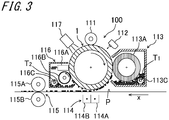
- the image forming apparatus illustrated in FIG. 3 employs a Carlson method as an image forming method and includes the electrophotographic photoreceptor 1, a charging device including a charging roller 111, a non-contact exposure device 112, a developing device 113 including a developing roller 113A and a toner transporting screw 113C for stirring unused toner T1, a transfer device 114, a fixing device 115 (115A and 115B), a cleaning device 116 including a cleaning blade 116A and a cleaning roller 116B which contact the electrophotographic photoreceptor and a toner transporting screw 116C for discharging residual toner T2, and a non-contact static eliminating device 117.
- the arrow x in the drawing indicates the moving direction of the paper which is the recording medium P.
- the charging device 111 has a function of charging the surface of the electrophotographic photoreceptor 1 to either positive or negative polarity.
- the charging voltage is set to, for example, 200 V or more and 1000 V or less.
- a contact charging device configured by covering a core metal with a conductive rubber or polyvinylidene fluoride (PVDF) is employed.
- PVDF polyvinylidene fluoride
- a non-contact charging device for example, a corona charging device including a discharge wire may be employed.
- the exposure device 112 has a function of forming an electrostatic latent image on the electrophotographic photoreceptor 1. Specifically, the exposure device 112 irradiates the electrophotographic photoreceptor 1 with exposure light (for example, laser light) having a specific wavelength (for example, 650 nm or more and 780 nm or less) according to an image signal to attenuate the potential of the exposure light irradiated portion of the electrophotographic photoreceptor 1 which is in a charged state, so that an electrostatic latent image is formed.
- exposure light for example, laser light
- a specific wavelength for example, 650 nm or more and 780 nm or less
- the light source of the exposure device 112 a light source capable of emitting a laser beam can be used instead of the LED element. That is, instead of the exposure device 112 such as the LED head, an optical system including a polygon mirror may be used.
- the image forming apparatus can be configured as a copier by employing an optical system including a mirror and a lens through which light reflected from a document passes.
- the developing device 113 has a function of developing an electrostatic latent image of the electrophotographic photoreceptor 1 to form a toner image.
- the developing device 113 in the example is provided with a magnetic roller 113A that retains the developer (toner) T magnetically.
- the developer (toner) T constitutes a toner image formed on the surface of the electrophotographic photoreceptor 1 and is frictionally charged in the developing device 113.
- the developer T there are exemplified a two-component developer including a magnetic carrier and an insulating toner and a one-component developer including a magnetic toner.
- the unused toner in the developing device 113 is indicated by T1
- the remaining (used) toner in the cleaning device 116 is indicated by T2.
- the magnetic roller 113A has a function of transporting the developer to the surface (developing region) of the electrophotographic photoreceptor 1.
- the magnetic roller 113A transports the developer T, which is frictionally charged in the developing device 113, in the form of a magnetic brush adjusted to a constant brush length.
- the transported developer T adheres to the surface of the electrophotographic photoreceptor 1 by electrostatic attraction with the electrostatic latent image in the developing region of the electrophotographic photoreceptor 1 to form a toner image (to visualize the electrostatic latent image).
- the charge polarity of the toner image is set to be opposite to the charge polarity of the surface of the electrophotographic photoreceptor 1.
- the charge polarity of the toner image is set to be the same as the charge polarity of the surface of the electrophotographic photoreceptor 1.
- the developing device 113 employs a dry development method in the present example, a wet development method using a liquid developer may be employed.
- a transporting screw 113C spiral type for stirring the unused toner T1 is arranged.
- the transfer device 114 has a function of transferring the toner image of the electrophotographic photoreceptor 1 to the recording medium P supplied to a transfer region between the electrophotographic photoreceptor 1 and the transfer device 114.
- the transfer device 114 in the present example includes a transfer charger 114A and a separation charger 114B.
- the back surface (non-recording surface) of the recording medium P is charged to have the charge polarity opposite to the charge polarity of the toner image in the transfer charger 114A, and the toner image is transferred on the recording medium P by the electrostatic attraction between the charged charge and the toner image.
- the back surface of the recording medium P is AC-charged in the separation charger 114B simultaneously with the transfer of the toner image, and the recording medium P is quickly separated from the surface of the electrophotographic photoreceptor 1.
- a transfer roller which follows the rotation of the electrophotographic photoreceptor 1 and which is arranged via a minute gap (for example, 0.5 mm or less) with the electrophotographic photoreceptor 1 may be used.
- the transfer roller is configured so that, for example, by a DC power supply applies a transfer voltage for attracting the toner image on the electrophotographic photoreceptor 1 onto the recording medium P.
- a transfer separation device such as the separation charger 114B can be omitted.
- the fixing device 115 has a function of fixing the toner image transferred to the recording medium P to the recording medium P and includes a pair of fixing rollers 115A and 115B.
- the fixing rollers 115A and 115B are obtained, for example, by coating the surface of a metal roller with tetrafluoroethylene or the like.
- the fixing device 115 can fix the toner image on the recording medium P by applying heat and pressure to the recording medium P passing between the pair of fixing rollers 115A and 115B.
- the cleaning device 116 has a function of removing toner remaining on the surface of the electrophotographic photoreceptor 1 and includes a cleaning roller 116B and a cleaning blade 116A.
- the cleaning roller 116B is in a shape of a crown having a large diameter at the center and slidingly contacts the outer circumference of the electrophotographic photoreceptor 1 and forms a toner film for surface cleaning, which is made of residual toner T2 therebetween.
- the cleaning blade 116A has a function of scraping the residual toner from the surface of the electrophotographic photoreceptor 1.
- the cleaning blade 116A is made of, for example, a rubber material containing a polyurethane resin as a main component.
- the static eliminating device 117 has a function of removing surface charges of the electrophotographic photoreceptor 1.
- the static eliminating device can emit light having a specific wavelength (for example, 630 nm or more).
- the static eliminating device 117 is configured to remove the surface charges (remaining electrostatic latent image) of the electrophotographic photoreceptor 1 by irradiating the entire surface of the electrophotographic photoreceptor 1 in the axial direction with light from a light source such as an LED.
- the electrophotographic photoreceptor 1 according to the embodiment of the invention was evaluated as follows.
- the cylindrical substrate 10 was manufactured by using an aluminum alloy raw tube (outside diameter: 30 mm and length: 360 mm). The outer surface of the cylindrical substrate 10 was subjected to surface mirroring processing and wet blasting processing to be cleaned.
- the cylindrical substrate 10 was retained at the two ends thereof, and in the state of rotating at a high speed of 1500 to 8000 rpm, the diamond turning tool was pressed against the cylindrical substrate 10, and a vanishing process was carried out at a feed of 0.08 to 0.5 mm. That is, a smooth finished surface was obtained by pressing the surface of the cylindrical substrate 10 with a diamond turning tool having a depth in the direction of work rotation on the finished surface of the turning tool.
- the cylindrical substrate 10 was degreased and cleaned.
- a high-hardness abrasive such as alumina and water are stirred and accelerated while being mixed with compressed air, and the surface of the surface-mirroring-processed cylindrical substrate 10 was roughened by projecting the abrasive. Accordingly, by processing while rotating the cylindrical substrate 10, it is possible to form a processed surface with excellent uniformity in a short time.
- uniformly projecting the abrasive having a small particle size can be relatively easily carried out, so that it is possible to obtain a processed surface with excellent uniformity.
- samples of the cylindrical substrate 10 including 15 types of different surfaces listed in Table 2 described below were prepared by adjusting the following parameters as the conditions for the wet blasting processing (Example 1).
- the value of Sal was adjusted by using abrasives having different materials and particle sizes, and the value of Str was adjusted by changing the projection air pressure, the projection distance, and the projection time (1 to 60 seconds).
- the used abrasive (medium) is washed away from the surface of the work by washing with water (coarse water washing) to be recovered and classified by centrifugation or the like to be reused. That is, in the wet blasting processing, the coarse water washing is carried out in the blasting apparatus in order to minimize the fluctuation of the concentration of the abrasive in the blast flow.
- cleaning is carried out by projecting the remaining water (containing small diameter abrasives and, hereinafter, is called "classification water") after the classification of the relatively large-diameter abrasives by centrifugation from the water containing the abrasives used for the blasting on the substrate (raw tube) immediately after blasting.
- classification water the remaining water
- the concentration in the blast flow of the abrasive is maintained.
- the residue remaining on the surface is cleaned and removed to prepare the cylindrical substrate 10 for forming the surface layer.
- the cleaning to remove the residue is carried out in the order of shower cleaning with water - ultrasonic cleaning - blowing (blowing with compressed air) - heater drying.
- the cylindrical substrate 10 prepared in this manner is transported into a clean room, subjected to precision cleaning for removing oil components and the like, and then set in the plasma CVD apparatus illustrated in FIG. 2 .
- the surface layer 13 including the charge injection blocking layer 11a, the photoconductive layer 11b, and the surface protective layer 12 is formed on the surface of the cylindrical substrate 10 under the conditions listed in Table 1.
- the flow rates of B 2 H 6 and NO in Table 1 are expressed as a ratio to the flow rate of SiH 4 .
- a DC pulse power supply (pulse frequency: 50 kHz, duty ratio: 70%) was used as a power supply of the plasma CVD apparatus.
- the film thickness was measured by analyzing the cross section with a scanning electron microscope (SEM) and an X-ray microanalyzer (XMA). The specific configuration of each layer is as follows.
- the charge injection blocking layer 11a is formed by adding boron (B) as a dopant to an amorphous silicon (a-Si)-based material obtained by adding nitrogen (N) and oxygen (O) to amorphous silicon (a-Si).
- the film thickness of the charge injection blocking layer 11a was set to 5 ⁇ m.
- the photoconductive layer 11b is formed by adding boron (B) as a dopant to an amorphous silicon (a-Si)-based material obtained by adding carbon (C), nitrogen (N), oxygen (O), and the like to amorphous silicon (a-Si).
- the film thickness of the photoconductive layer 11b was set to 14 ⁇ m.
- the surface protective layer 12 has a configuration in which amorphous silicon carbide (a-SiC) and amorphous carbon (a-C) are stacked.
- a-SiC amorphous silicon carbide
- a-C amorphous carbon
- the film thickness of the surface protective layer 12 was set to 1.2 ⁇ m in total, and the film thickness of the surface protective layer third layer was set to 0.2 ⁇ m.
- Samples 1 to 15 of the electrophotographic photoreceptor 1 were produced by changing the surface roughness of the surface protective layer 12.
- the Str and Sal of each sample are as listed in Table 2 described below.
- each sample of the manufactured electrophotographic photoreceptor 1 was incorporated into a color multifunction apparatus "TASKalfa 3550ci remodeling apparatus" manufactured by KYOCERA Document Solutions Inc., and for each sample, evaluation of an Sa reduction rate (%) of the surface protective layer 12 of the electrophotographic photoreceptor 1, evaluation of a scratch of the cleaning blade 116A, which is a peripheral member of the electrophotographic photoreceptor 1, and evaluation of the image characteristics by observing the surface contamination state of the charging roller at the time of continuous printing of 600,000 sheets (600K) were carried out. Then, comprehensive evaluation was carried out, which is comprehensive evaluation on the basis of those individual characteristics.
- TASKalfa 3550ci remodeling apparatus manufactured by KYOCERA Document Solutions Inc.
- Evaluation of each of the above-mentioned individual characteristics was carried out under the condition of the following. That is, under the evaluation environment of a room temperature of 23°C and a relative humidity of 60%, at the time of continuous printing of 200,000 sheets, the time of continuous printing of 400,000 sheets, and the time of continuous printing of 600,000 sheets, the measurement of the surface texture of the electrophotographic photoreceptor 1 by the above-mentioned laser microscope and the observation of the presence or absence of scratches on the edge portion of the cleaning blade 116A and the surface contamination state of the charging roller by a magnifying glass (20-fold magnification) were carried out.
- the Sa reduction rate (%) indicates the rate at which the value of Sa on the surface protective layer of the electrophotographic photoreceptor 1 is reduced from the initial value before the printing, and, for example, a case where the rate is described as 70% denotes that the value of Sa is 30% of that in the state before printing.
- the value marked with "*" indicates the Sa reduction rate (%) of the surface protective layer 12 of the electrophotographic photoreceptor 1 at the time of continuous printing of 200,000 sheets (200K).
- a damage mode of the cleaning blade 116A is as follows. Evaluation A indicates that, as a result of continuous printing of 200,000 sheets (200K), some damages were observed on the cleaning blade 116A. Evaluation B indicates that clear damages were able to be seen on the cleaning blade 116A at the time of small number of times of printing of 1000 sheets or less.
- the surface shape of the surface protective layer 12 has unevenness with high uniformity, so that the surface roughness can be maintained within a certain range even when the surface is gradually abraded during durable use.
- the defect of the cleaning blade 116A can be suppressed, and thus, image abnormalities such as abnormal streaks in the printed image can be reduced.
- the cause of the initial defect in Samples 14 and 15 when the value of Sal is large, the frictional resistance with the cleaning roller and cleaning blade as peripheral members is large, and thus the defect of the cleaning blade 116A occurs.
- Example 2 will be described in which the surface roughness is changed in the cylindrical axial direction (the width direction of the cylinder) in response to the peripheral members arranged around the electrophotographic photoreceptor.
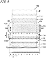
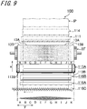
- FIGS. 4 to 11 are exploded perspective views illustrating the relationship between the surface roughness of the electrophotographic photoreceptors (1A to 1H) according to the first to eighth embodiments of the invention before forming the surface layer and the peripheral members arranged around the electrophotographic photoreceptors.
- each figure illustrates that various peripheral members arranged in a contact/non-contact manner around the rotation axis of the electrophotographic photoreceptor 1 are actually developed in the same plane and arranged in a line as illustrated in FIG.
- the change of the roughness (surface roughness) of the outer surface in the width direction (y direction) appears stepwise due to hatching (point density), but in the actual change of the surface roughness (surface roughness profile), as illustrated in the schematic views in the lower portion of each drawing, the surface roughness is designed such that the roughness changes gradually in the axial direction (y direction), that is, gradually or gently in the cylindrical axial direction.
- the portion of the electrophotographic photoreceptor not drawn with hatching is a surface (substrate mirror surface portion where wet-blasting is not carried out) on which Sa after the surface mirroring processing is less than 25 nm as described above and the surface of the surface layer 13 is a "surface-layer surface mirror surface portion (reference numeral 13B)" of Sa ⁇ 25 nm after the surface layer is formed (refer to Paragraph [0017]).
- the symbols A to K representing sections (blocks) are provided to make it easy to see the positional relationship in the width direction between the exploded perspective view and the schematic view. It does not mean that the change in roughness in the cylindrical axial direction (y direction in the figure) changes stepwise in units of a block.
- the "image printing portion" in which the toner is actually transferred to the sheet corresponds to the illustrated blocks B to J.
- the electrophotographic photoreceptor 1A according to the first embodiment illustrated in FIG. 4 is configured by using a cylindrical substrate 10 (raw tube) including an outer surface of a surface roughness profile as illustrated in the schematic view. That is, the electrophotographic photoreceptor 1A is formed based on a raw tube which has outer surface roughness (arithmetic mean height Sa) of, for example, 70 nm in the central portion of the substrate in the cylindrical axial direction and less than 25 nm in one substrate end portion (block A in the left side illustrated in the figure) of both end portions in the axial direction and whose surface roughness of the substrate central portion is larger than the surface roughness of one substrate end portion.
- outer surface roughness arithmetic mean height Sa
- the surface roughness of the surface layer 13 of the electrophotographic photoreceptor 1A after the film formation also conforms to the surface shape of the cylindrical substrate 10 (raw tube), and the surface roughness of the surface-layer central portion is larger than the surface roughness of one surface-layer end portion.
- the image printing portions (blocks B to J) in the surface layer 13 of the electrophotographic photoreceptor 1A are rough surfaces having a surface roughness Str of 0.67 or more.
- the boundary (block B) between the block A which is a mirror surface portion of the substrate having an Sa of less than 25 nm and the block C which is a rough surface is formed to have a roughness gradient surface where the surface roughness gradually increases from the mirror surface to the rough surface as illustrated in the surface roughness profile in FIG. 4 . Therefore, peeling of the film (surface layer) at the boundary portion between the mirror surface and the rough surface is less likely to occur.
- the block A (surface-layer mirror surface portion described below) which is a mirror surface is provided with an identification portion M having a surface roughness larger than that of the mirror surface at one place in the circumferential direction.
- This identification portion may be, for example, an individual identification code portion for identifying each of the electrophotographic photoreceptors as illustrated in FIG. 4 .
- the individual identification code portion is a barcode using surface roughness (striations) that changes in the circumferential direction.
- the identification portion may be a guide mark portion serving as an index of circumferential rotation of the cylindrical substrate.
- the identification portion M functions as the individual identification code and the reference standard of rotation speed measurement of the circumferential direction rotation.
- a portion (surface area) where the arithmetic mean height Sa of the surface is less than 25 nm is referred to as a "surface-layer mirror surface portion" (reference numeral 13B).
- the rollers 113B and 113B which regulate the gap (developing gap) between the electrophotographic photoreceptor 1A and the magnetic roller 113A in the developing device 113 at the two ends by the contact and the above-described guide mark portion M are at the same position in the cylindrical width direction, the roller 113B rides on the guide mark portion M, and thus, the distance (gap) between the electrophotographic photoreceptor 1A and the magnetic roller 113A changes.
- the guide mark portion M is provided in the surface-layer mirror surface portion 13B (block A) at a position out of the position (outer edge) where the roller 113B abuts.
- the electrophotographic photoreceptor having the above-described configuration, in a case where the electrophotographic photoreceptor is used as an image forming apparatus as illustrated in the figure, as described above, the peeling of the film (surface layer) at the boundary portion between the mirror surface and the rough surface is unlikely to occur, and it is possible to prevent image abnormalities caused by the peeled fragments from occurring in advance.
- the outermost surface (outer circumferential surface of surface layer 13) of the image printing portion (blocks B to J) that contacts the peripheral members such as the cleaning roller (sliding roller) and the cleaning blade is formed to be a rough surface having a surface roughness Str ⁇ 0.67.
- the electrophotographic photoreceptor 1B addresses a case where a larger amount of the used residual toner T2 used as an external additive for cleaning (sliding and polishing) the surface of the electrophotographic photoreceptor illustrated in FIG. 3 is retained on the toner discharge side (left side in FIG. 5 ) in the box structure constituting the cleaning device 116, and thus, more friction (abrasion) is generated on the surface (left side in FIG. 5 ) of the electrophotographic photoreceptor on the toner retention side.
- the electrophotographic photoreceptor 1B according to the second embodiment is configured by using a cylindrical substrate 10 (raw tube) including the outer surface of the surface roughness profile as illustrated in FIG. 5 . That is, the electrophotographic photoreceptor 1B is formed based on a raw tube which has outer surface roughness which gradually decreases from the other end (second substrate end portion, block K in the right side of the figure) of two substrate end portions in the cylindrical axial direction to one end (first substrate end portion, block A of a mirror surface illustrated in the figure) thereof.
- the surface roughness of the surface layer 13 of the electrophotographic photoreceptor 1B after the film formation also conforms to the surface shape of the cylindrical substrate 10 (raw tube), and the surface roughness gradually decreases from the other end (second surface-layer end portion, a block K on the right side in the figure) of the two surface-layer end portions in the cylindrical axial direction toward one end portion (first surface-layer end portion, a block A of the mirror surface on the left side in the figure) thereof.
- the surface roughness Sa of the cylindrical substrate 10 (raw tube) of the electrophotographic photoreceptor 1B is, for example, less than 25 nm in the block A at the left end (substrate mirror surface portion) and 119 nm in the block K at the right end.
- the image printing portion (blocks B to J) in the surface layer 13 of the electrophotographic photoreceptor 1B is a rough surface having a surface roughness Str of 0.67 or more, and the boundary portion between the mirror surface and the rough surface (between the block A and the block B) is formed to be a roughness gradient surface where the surface roughness gradually increases toward the right side similarly to the raw tube according to the first embodiment.
- the electrophotographic photoreceptor having the above-described configuration, when the electrophotographic photoreceptor is used as an image forming apparatus, similarly to the previous embodiment, it is possible to prevent the peeling of the film (surface layer) at the boundary portion between the mirror surface and the rough surface.
- the outermost surface (the outer circumferential surface of the surface layer 13) of the image printing portion (blocks B to J) is formed to be a rough surface whose surface roughness Str gradually decreases from the other end (second surface-layer end portion) on the right side to one end (first surface-layer end portion on the toner discharge side) on the left side. Therefore, as illustrated in FIG.
- the electrophotographic photoreceptor may be configured like the electrophotographic photoreceptor 1C according to the third embodiment illustrated in FIG. 6 .
- the roughness change profile of the outer surface of the electrophotographic photoreceptor 1C ( FIG. 6 ) and the roughness change of the surface layer 13 of the electrophotographic photoreceptor 1C after the film formation in the cylindrical axial direction, which roughness change conforms to the roughness change profile, are also formed more gently than those of the electrophotographic photoreceptors 1A and 1B according to the first and second embodiments.
- the roughness change (profile) of the outer surface of the electrophotographic photoreceptor 1C and the roughness change of the surface layer 13 of the electrophotographic photoreceptor 1C in the cylindrical axial direction which conforms to the roughness change (profile) of the outer surface gradually increases from the first end portion on the left side (first substrate end portion and first surface-layer end portion) to the central portion (substrate central portion and surface-layer central portion), and in the right half in the figure, the surface roughness hardly change in the surface-layer central portion.
- the surface roughness Sa of the cylindrical substrate 10 (raw tube) of the electrophotographic photoreceptor 1C is, for example, 75 nm in the block A at the left end and 90 nm in the block F at the substrate central portion.
- the surface roughness Str of the image printing portions (blocks B to J) in the surface layer 13 of the electrophotographic photoreceptor 1C after the film formation is 0.91 in the block B on the left and 0.93 in the block F in the surface-layer center.
- the change in the surface roughness Str of the surface layer is gentle, so that it is possible to prevent the peeling of the film (surface layer) due to the aged use.
- the electrophotographic photoreceptor may be configured like the electrophotographic photoreceptor 1D according to the fourth embodiment illustrated in FIG. 7 .
- each of the electrophotographic photoreceptors 1E to 1H is formed based on a raw tube whose roughness (arithmetic mean height Sa) of the outer surface gradually increases from the first substrate end portion (block A on the left side) of one end in the cylindrical axial direction and the second substrate end portion (block K on the right side) of the other end in the axial direction toward the block F of the central portion (substrate central portion) in the axial direction.
- the surface roughness of the surface layer 13 of each of the electrophotographic photoreceptors 1E to 1H after the film formation also has a shape conforming to the surface shape of the cylindrical substrate 10 (raw tube).
- two rollers 113B and 113B arranged at the two ends of the magnetic roller 113A abut on the outer edge portions at the two ends of the electrophotographic photoreceptor 1E. Therefore, the gap (developing gap) between the magnetic roller 113A and the electrophotographic photoreceptor 1E is regulated, which addresses the occurrence of a large amount of abrasion on the outer edge portions.
- the electrophotographic photoreceptor 1E is formed based on a raw tube in which the surface roughness of the substrate central portion (blocks B to J in the figure) of the outer surface is larger than the surface roughness of one end (first substrate end portion, a block A of the mirror surface on the left side in the figure) and the other end (second substrate end portion, a block K on the right side in the figure) of the two ends in the cylindrical axial direction of the outer surface.
- the surface roughness of the surface layer 13 of the electrophotographic photoreceptor 1E after the film formation also conforms to the surface shape of the cylindrical substrate 10 (raw tube), and the surface roughness of the surface-layer central portion (blocks B to J in the figure) is larger than the surface roughness of one end (first surface-layer end portion, a block A of the mirror surface on the left side in the figure) and the other end (second surface-layer end portion, a block K on the right side in the figure) of the two ends in the cylindrical axial direction.
- the surface roughness Sa of the cylindrical substrate 10 (raw tube) of the electrophotographic photoreceptor 1E is, for example, less than 25 nm at the blocks A and K (substrate mirror surface portion) of the substrate end portion and 60 nm at the blocks B to J at the substrate central portion.
- the image printing portions (blocks B to J) on the surface layer 13 of the electrophotographic photoreceptor 1E are rough surfaces having a surface roughness Str of 0.67 or more.
- the boundary portion between the mirror surface and the rough surface (between the blocks A and B and between the blocks J and K) is formed to be a roughness gradient surface where the surface roughness gradually increases toward the surface-layer central portion similarly to the raw tube according to the first embodiment.
- the outer edge portions at the two ends of the electrophotographic photoreceptor 1E that slidingly contacts the rollers 113B at the two ends of the magnetic roller 113A are mirror surfaces, there is less abrasion on the surface layer at these positions, and thus, initial performance can be maintained for a long time.
- the outermost surface (outer circumferential surface of surface layer 13) of the image printing portion (blocks B to J) that contacts the peripheral members such as the cleaning roller (sliding roller) and the cleaning blade is formed to be a rough surface with a surface roughness of Str ⁇ 0.67, even when the electrophotographic photoreceptor is used repeatedly many times, the image abnormalities are unlikely to occur, and the life of the electrophotographic photoreceptor 1E can be extended.
- the electrophotographic photoreceptor 1F addresses a case where the cleaning roller (sliding roller) 116B of the cleaning device 116 illustrated in FIG. 3 is in a shape such as a crown shape by taking into consideration of the abrasion of the central portion and the contact pressure to the electrophotographic photoreceptor 1F at the two ends of the cleaning roller 116B is increased.
- the electrophotographic photoreceptor 1F is formed based on a raw tube which has outer surface roughness gradually increases from one end (first substrate end portion, a block A of the mirror surface on the left side in the figure) and the other end (second substrate end portion, a block K on the right side in the figure) to the substrate central portion (F in the figure) of the two ends in the cylindrical axial direction.
- the surface roughness of the surface layer 13 of the electrophotographic photoreceptor 1E after the film formation also conforms to the surface shape of the cylindrical substrate 10 (raw tube), and the surface roughness gradually increases from one end (first surface-layer end portion, a block A of the mirror surface on the left side in the figure) and the other end (second surface-layer end portion, a block K on the right side in the figure) of the two ends in the cylindrical axial direction toward the surface-layer central portion (F in the figure)
- the surface roughness Sa of the cylindrical substrate 10 (raw tube) of the electrophotographic photoreceptor 1F is, for example, less than 25 nm in the blocks A and K (substrate mirror surface portion) in the substrate end portion and 110 nm in the block F in the substrate central portion.
- the image printing portions (blocks B to J) in the surface layer 13 of the electrophotographic photoreceptor 1F are rough surfaces having a surface roughness Str of 0.67 or more, and the boundary portion between the mirror surface and the rough surfaces (between the blocks A and B and the blocks J and K) is formed to be a roughness gradient surface where the surface roughness gradually increases toward the surface-layer central portion similarly to the raw tube of the above-described embodiment.
- the outer edge portions at the two ends of the electrophotographic photoreceptor 1F that slidingly contacts the rollers 113B at the two ends of the magnetic roller 113A are mirror surfaces (surface-layer mirror surface portions 13B), there is less abrasion on the surface layer at these positions, and the initial performance can be maintained for a long time.
- the outermost surface (outer circumferential surface of surface layer 13) of the image printing portion (blocks B to J) that contacts peripheral members such as a cleaning roller (sliding roller) is formed to be a rough surface having a surface roughness Str ⁇ 0.67 and is formed to be a rough surface whose surface roughness Str increases toward the surface-layer central portion.
- the electrophotographic photoreceptor 1F can also be an electrophotographic photoreceptor with a long life.
- the electrophotographic photoreceptor 1G according to the seventh embodiment illustrated in FIG. 10 can be configured.
- the outermost surface (the outer circumferential surface of the surface layer 13) of the image printing portion (blocks B to J) that contacts the peripheral member such as the cleaning roller is formed to be a rough surface having a surface roughness of Str ⁇ 0.67 and is formed to be a rough surface whose surface roughness Str increases toward the surface-layer central portion.
- the surface roughness Sa of the cylindrical substrate 10 (raw tube) of the electrophotographic photoreceptor 1G is, for example, 60 nm in the blocks A and K at both left and right ends and 119 nm in the block F in the substrate central portion.
- the surface roughness Str of the image printing portions (blocks B to J) in the surface layer 13 of the electrophotographic photoreceptor 1G after the film formation is 0.89 in the left and right blocks A and K and 0.97 in the block F in the surface-layer central portion.
- the outermost surface (outer circumferential surface of the surface layer) of the image printing portion (blocks B to J) that contacts the crown-shaped cleaning roller has a surface roughness of Str ⁇ 0.67 and is formed to be a rough surface whose surface roughness gradually increases from the two surface-layer end portions to the surface-layer central portion, and thus, even in a case where the contact pressure to the electrophotographic photoreceptor 1G at the two ends of the cleaning roller 116B is set to be high, it is possible to reduce the abrasion of this portion having a high contact pressure. Therefore, the electrophotographic photoreceptor 1G can also be an electrophotographic photoreceptor with a long life.
- the electrophotographic photoreceptor 1H of the eighth embodiment illustrated in FIG. 11 addresses a case where the cleaning roller (sliding roller) 116B of the cleaning device 116 is in a crown shape by taking into consideration of the abrasion of the central portion and the outlet for an external additive (used residual toner T2) for cleaning the electrophotographic photoreceptor is provided on the left side in the figure.
- an external additive used residual toner T2
- the features of the surface roughness profile ( FIG. 11 ) of the outer circumferential surface of the electrophotographic photoreceptor 1H in the state of the raw tube (cylindrical substrate 10) before forming the surface layer are that a rough surface is formed such that the surface roughness gradually increases from the first substrate end portion (left side in the figure) of one end in the cylindrical axial direction and the second substrate end portion (right side in the figure) of the other end in the axial direction to the substrate central portion in the center in the axial direction and the maximum point of the surface roughness is arranged to be offset from the substrate central portion to the blocks G and H on the right side in the figure by taking into consideration of the abrasion which frequently occurs on the discharge side due to the retention of the used residual toner T2.
- the maximum point of the surface roughness is deviated to the right from the substrate central portion, and this is because, in the profile ( FIG. 9 ) of the eighth embodiment, similarly to the profile according to the preceding second embodiment (refer to FIG. 5 ), the surface roughness overlaps the profile gradually decreasing toward the left end (the first substrate end portion on the toner discharge side).
- the surface roughness Sa of the cylindrical substrate 10 (raw tube) of the electrophotographic photoreceptor 1H is, for example, less than 25 nm in the blocks A and K (substrate mirror surface) of the substrate end portion and 119 nm in the blocks G and H near the substrate central portion, and thus, the surface roughness of the surface layer 13 of the electrophotographic photoreceptor 1H after the film formation is also in a shape conforming to the surface shape of the cylindrical substrate 10 (raw tube).
- the image printing portions (blocks B to J) in the surface layer 13 of the electrophotographic photoreceptor 1H are rough surfaces having a surface roughness Str of 0.67 or more, and the Str of the blocks G and H located near the surface-layer center is 0.91.
- the boundary portion between the mirror surface and the rough surface is formed to be a roughness gradient surface where the surface roughness gradually increases toward the surface-layer central portion.
- the surface-layer mirror surface portion 13B (block A), which is a mirror surface on one end side, is provided with an identification portion M whose surface roughness is larger than that of the mirror surface at one location in the circumferential direction.
- This identification portion is provided at a position deviated from the position (outer edge in the figure) in which the roller 113B supporting the magnetic roller 113A abuts, and a bar code (individual identification code section) using surface roughness (line mark) that changes in the circumferential direction is formed.
- the outer edge portions at the two ends of the electrophotographic photoreceptor 1H that slidingly contacts the rollers 113B at the two ends of the magnetic roller 113A are mirror surfaces (surface-layer mirror surface portions 13B), so that there is less abrasion on the layer at this position.
- the outermost surface (the outer circumferential surface of the surface layer 13) of the image printing portion (blocks B to J) that contacts the peripheral member such as the cleaning roller is formed to be a rough surface having a surface roughness of Str ⁇ 0.67, even when the electrophotographic photoreceptor is used repeatedly many times, image abnormalities are unlikely to occur.
- an electrophotographic photoreceptor including a cylindrical substrate, and a surface layer located on an outer surface of the cylindrical substrate, in which at least in the substrate central portion in the cylindrical axial direction of the outer surface of the cylindrical substrate is formed as a rough surface, the surface roughness of the surface-layer central portion in the cylindrical axial direction of the outer surface of the surface layer is larger than that of at least one of the two surface-layer end portions in the cylindrical axial direction of the outer surface of the surface layer, and the surface roughness of the substrate central portion in the cylindrical axial direction of the outer surface of the cylindrical substrate is larger than that of at least one of the two substrate end portions in the axial direction of the outer surface of the cylindrical substrate.
- the technical scope claimed in the embodiment includes the electrophotographic photoreceptor in which the surface roughness of the outer surface of the cylindrical substrate gradually increases from the first substrate end portion to the second substrate end portion of the both substrate end portions.
- the technical scope claimed in the embodiment includes the electrophotographic photoreceptor in which the surface roughness of the outer surface of the cylindrical substrate gradually increases from at least one of both substrate end portions to the substrate central portion.
- the technical scope claimed in the embodiment includes the electrophotographic photoreceptor in which at least one of both substrate end portions of the outer surface of the cylindrical substrate includes a substrate mirror surface portion including a mirror surface having a surface roughness of Sa ⁇ 25 nm.
- the technical scope claimed in the embodiment includes the electrophotographic photoreceptor in which the substrate mirror surface portion includes the identification portion whose surface roughness is larger than that of the mirror surface at a portion excluding an outer edge in the cylindrical axial direction.
- the cylindrical substrate 10, the charge injection blocking layer 11a, and the photoconductive layer 11b are described as separate components, but alternatively, at least the surface of the cylindrical substrate 10 may have a charge injection blocking characteristic.
- the cylindrical substrate 10 itself can have a function of blocking injection of carriers (electrons) from the cylindrical substrate 10 to the photoconductive layer 11b without separately providing the charge injection blocking layer 11a.
Landscapes
- Physics & Mathematics (AREA)
- General Physics & Mathematics (AREA)
- Chemical & Material Sciences (AREA)
- Inorganic Chemistry (AREA)
- Photoreceptors In Electrophotography (AREA)
Abstract
Description
- The present invention relates to an electrophotographic photoreceptor and an image forming apparatus including the same.
- In the related art, an electrophotographic photoreceptor has a configuration in which a surface layer including a charge injection blocking layer, a photoconductive layer, a surface protective layer, and the like is formed on the surface of a cylindrical substrate and the like as described in, for example, Patent Literature 1 (for example,
Patent Literatures 1 to 4). -
- Patent Literature 1: Japanese Unexamined Patent Publication
JP-A 63-129348 - Patent Literature 2: Japanese Unexamined Patent Publication
JP-A 2011-221144 - Patent Literature 3: Japanese Unexamined Patent Publication
JP-A 2016-186574 - Patent Literature 4: Japanese Unexamined Patent Publication
JP-A 2006-119549 - An electrophotographic photoreceptor according to the present disclosure includes a cylindrical substrate and a surface layer located on an outer surface of the cylindrical substrate. At least a substrate central portion in a cylindrical axial direction of the outer surface of the cylindrical substrate is formed as a rough surface. A surface roughness of a surface-layer central portion in a cylindrical axial direction of an outer surface of the surface layer is larger than that of at least one of two surface-layer end portions in the cylindrical axial direction of the outer surface of the surface layer.
- An image forming apparatus according to the present disclosure includes the above-described electrophotographic photoreceptor, and a peripheral member capable of contacting the electrophotographic photoreceptor.
-
-
FIG. 1A is a cross-sectional view illustrating an electrophotographic photoreceptor according to an embodiment; -
FIG. 1B is a cross-sectional view of a principal portion ofFIG. 1A ; -
FIG. 2 is a longitudinal cross-sectional view of a deposition film forming apparatus; -
FIG. 3 is a cross-sectional view illustrating an image forming apparatus according to the embodiment; -
FIG. 4 is an exploded perspective view illustrating a relationship between surface roughness of an electrophotographic photoreceptor according to a first embodiment and peripheral members and a schematic view visually illustrating a change in surface roughness of the outer circumferential surface of acylindrical substrate 10 of anelectrophotographic photoreceptor 1A in the width direction as a difference between a peak and a valley; -
FIG. 5 is an exploded perspective view illustrating a relationship between surface roughness of an electrophotographic photoreceptor according to a second embodiment and peripheral members and a schematic view visually illustrating a change in surface roughness of the outer circumferential surface of acylindrical substrate 10 of anelectrophotographic photoreceptor 1B in the width direction as a difference between a peak and a valley; -
FIG. 6 is an exploded perspective view illustrating a relationship between surface roughness of an electrophotographic photoreceptor according to a third embodiment and peripheral members and a schematic view visually illustrating a change in surface roughness of the outer circumferential surface of acylindrical substrate 10 of anelectrophotographic photoreceptor 1C in the width direction as a difference between a peak and a valley; -
FIG. 7 is an exploded perspective view illustrating a relationship between surface roughness of an electrophotographic photoreceptor according to a fourth embodiment and peripheral members and a schematic view visually illustrating a change in surface roughness of the outer circumferential surface of acylindrical substrate 10 of anelectrophotographic photoreceptor 1D in the width direction as a difference between a peak and a valley; -
FIG. 8 is an exploded perspective view illustrating a relationship between surface roughness of an electrophotographic photoreceptor according to a fifth embodiment and peripheral members and a schematic view visually illustrating a change in surface roughness of the outer circumferential surface of acylindrical substrate 10 of anelectrophotographic photoreceptor 1E in the width direction as a difference between a peak and a valley; -
FIG. 9 is an exploded perspective view illustrating a relationship between surface roughness of an electrophotographic photoreceptor according to a sixth embodiment and peripheral members and a schematic view visually illustrating a change in surface roughness of the outer circumferential surface of acylindrical substrate 10 of anelectrophotographic photoreceptor 1F in the width direction as a difference between a peak and a valley; -
FIG. 10 is an exploded perspective view illustrating a relationship between surface roughness of an electrophotographic photoreceptor according to a seventh embodiment and peripheral members and a schematic view visually illustrating a change in surface roughness of the outer circumferential surface of acylindrical substrate 10 of anelectrophotographic photoreceptor 1G in the width direction as a difference between a peak and a valley; and -
FIG. 11 is an exploded perspective view illustrating a relationship between surface roughness of an electrophotographic photoreceptor according to an eighth embodiment and peripheral members and a schematic view visually illustrating a change in surface roughness of the outer circumferential surface of acylindrical substrate 10 of anelectrophotographic photoreceptor 1H in the width direction as a difference between a peak and a valley. - Hereinafter, an electrophotographic photoreceptor according to an embodiment and an image forming apparatus provided with the same will be described with reference to the drawings. In addition, the following contents illustrate embodiments of the invention, and the invention is not limited to examples of the embodiments.
- An electrophotographic photoreceptor according to the embodiment will be described with reference to
FIGS. 1A and1B . - The
electrophotographic photoreceptor 1 illustrated inFIGS. 1A and1B includes a photosensitive layer 11 in which a chargeinjection blocking layer 11a and aphotoconductive layer 11b are sequentially formed, on the outer surface of acylindrical substrate 10. A surfaceprotective layer 12 is deposited on the outer surface of the photosensitive layer 11. In addition, herein, asurface layer 13 includes the photosensitive layer 11 and the surfaceprotective layer 12. - The
cylindrical substrate 10 is a support of the photosensitive layer 11, and at least the surface of thecylindrical substrate 10 has conductivity. - The
cylindrical substrate 10 is formed as a substrate having conductivity as a whole, for example, by using a metal material such as aluminum (Al), stainless steel (SUS), zinc (Zn), copper (Cu), iron (Fe), titanium (Ti), nickel (Ni), chromium (Cr), tantalum (Ta), tin (Sn), gold (Au), silver (Ag), magnesium (Mg), and manganese (Mn) or an alloy material containing the exemplified metal materials. In addition, thecylindrical substrate 10 may be a substrate formed by depositing a conductive film made of the exemplified metal material and a transparent conductive material such as ITO (indium tin oxide) or SnO2 (tin dioxide) on the surface made of a resin, glass, or ceramics. Among these exemplified materials, an aluminum (Al)-based material may be used as a material for forming thecylindrical substrate 10, and the entirecylindrical substrate 10 may be formed by using the aluminum (Al)-based material. Then, theelectrophotographic photoreceptor 1 can be manufactured at a low weight and at a low cost. Furthermore, in a case where the chargeinjection blocking layer 11a and thephotoconductive layer 11b are formed by using an amorphous silicon (a-Si)-based material, the adhesion between the layers and thecylindrical substrate 10 becomes high, so that it is possible to improve the reliability. - The surface of the
cylindrical substrate 10 may be roughened. The surface roughness of thecylindrical substrate 10 may be, for example, 50 nm < Sa < 140 nm after roughening. In addition, as a method of roughening, for example, wet blast, sputter etching, gas etching, polishing, turning, wet etching, electric galvanic corrosion, or the like may be used. A drawn pipe that satisfies the above-mentioned surface roughness may be used as it is without performing surface treatment for adjusting the surface shape. In addition, in the invention, a portion (surface area) where the arithmetic mean height Sa of the surface is 25 nm or more is called a "rough surface". - In addition, the surface of the
cylindrical substrate 10 may be surface-mirroring-processed before the above-mentioned surface roughening, but in such a case, it is preferable to perform oil removal after the surface mirroring processing before the surface roughening. Furthermore, the surface roughness of thecylindrical substrate 10 may be, for example, Sa < 25 nm after the surface mirroring processing. In addition, in the invention, a portion (surface area) where the arithmetic mean height Sa of the surface is less than 25 nm is referred to as a "mirror surface". - In the present specification, Sa (arithmetic mean roughness) is one of the parameters representing a three-dimensional surface texture defined by ISO25178 and represents the arithmetic mean roughness (nm) of the absolute value of the height of the surface in the measurement target region from the average surface. In addition, the measurement as the evaluation of the surface shape with the three-dimensional roughness parameter based on ISO25178 was carried out by a three-dimensional measurement laser microscope OLS4100 produced by Olympus Co., Ltd described below. In addition, the measurement of the electrophotographic photoreceptor (surface layer) was carried out on the product surface as it is, and the measurement of the outer surface (outer circumferential surface) of the cylindrical substrate under the surface layer was carried out after removing the surface layer from the product of the electrophotographic photoreceptor by dry etching using ClF3, CF4, or the like.
- In addition, the surface texture of the
electrophotographic photoreceptor 1 needs not to satisfy a predetermined range over the entire surface of the surfaceprotective layer 12. For example, in both end portions or the like of thecylindrical substrate 10 in the axial direction which do not contact thecleaning roller 116B or thecleaning blade 116A, the surface texture may have a value out of the range. This is the same for all the parameters of the surface texture described below. - The charge
injection blocking layer 11a has a function of blocking injection of carriers (electrons) from thecylindrical substrate 10. The chargeinjection blocking layer 11a is made of, for example, an amorphous silicon (a-Si)-based material. The chargeinjection blocking layer 11a may be formed, for example, by using an amorphous silicon (a-Si) containing nitrogen (N) or oxygen (O) or both in the case of containing boron (B) as a dopant or by using an amorphous silicon (a-Si) containing nitrogen (N) or oxygen (O) or both in the case of containing phosphorus (P) as a dopant, and the thickness thereof is set to 2 µm or more and 10 µm or less. - The
photoconductive layer 11b has a function of generating carriers by light irradiation such as laser light. Thephotoconductive layer 11b is made of, for example, an amorphous silicon (a-Si)-based material and an amorphous selenium (a-Se)-based material such as Se-Te or As2Se3. Thephotoconductive layer 11b in the present example is made of amorphous silicon (a-Si) and an amorphous silicon (a-Si)-based material obtained by adding carbon (C), nitrogen (N), oxygen (O), and the like to amorphous silicon (a-Si) and contains boron (B) or phosphorus (P) as a dopant. - In addition, the thickness of the
photoconductive layer 11b may be appropriately set in accordance with the photoconductive material to be used and the desired electrophotographic characteristics. In a case where thephotoconductive layer 11b is formed by using an amorphous silicon (a-Si)-based material, the thickness of thephotoconductive layer 11b may be set to, for example, 5 µm or more and 100 µm or less, and more specifically 10 µm or more and 80 µm or less. - The surface
protective layer 12 has a function of protecting the surface of the photosensitive layer 11. The surfaceprotective layer 12 may be formed by using an amorphous silicon (a-Si) material such as amorphous silicon carbide (a-SiC) or amorphous silicon nitride (a-SiN) or amorphous carbon (a-C) or may be formed to have a multi-layer structure thereof. In the example, the surfaceprotective layer 12 is formed to have a three-layer structure, and the third layer of the surfaceprotective layer 12 which is the outermost surface after the surface layer formation is formed by employing high-resistant amorphous carbon (a-C) from the point of view of abrasion resistance against rubbing in the image forming apparatus. - The thickness of the surface
protective layer 12 may be adjusted, for example, in accordance with the required number of durable electrophotographic photoreceptors, and it is not necessary to increase the thickness more than necessary. For example, the thickness may be set to 0.1 µm or more and 2 µm or less, and more specifically to 0.5 µm or more and 1.5 µm or less. - In the embodiment, the surface roughness of the surface
protective layer 12 may be set to Str ≥ 0.67, and more specifically to Str ≥ 0.79. Accordingly, it is possible to exhibit excellent durability characteristics and to suppress the occurrence of an image abnormality. That is, it is possible to suppress the frictional resistance with the cleaning roller, the cleaning blade, and the like in the initial stage, and it is possible to maintain the surface roughness within a certain range even when the surface is gradually abraded during durable use. As a result, since it is possible to continue to effectively suppress the increase in the frictional resistance between the surface protective layer and the cleaning roller or the cleaning blade, it is possible to suppress image abnormalities such as abnormal streaks in the printed image. - In addition, the surface roughness of the surface
protective layer 12 may be set to Sal ≤ 10.3 µm. Furthermore, the surface roughness of the surfaceprotective layer 12 may be set to Sal ≥ 0.9 µm, and more specifically, may be set to Sal ≥ 1.6 µm. Accordingly, it is possible to more effectively exhibit the above-described excellent durability characteristics and the reduction in image abnormality. That is, in the planar direction of the surface of the surface protective layer, due to the presence of the unevenness at a narrow pitch defined by the above-mentioned numerical values, it is possible to realize the reduction of the initial defect and the suppression of the increase in the frictional resistance during durable use. - In addition, in the present specification, Str (aspect ratio of surface texture) is one of the parameters representing the three-dimensional surface texture defined by ISO25178 and represents the aspect ratio of the surface texture. That is, Str is a scale that represents the uniformity of the surface texture, and the autocorrelation of the surface is defined by the ratio of the farthest lateral distance to the correlation value 0.2 to Sal. Str has a value in a range of 0 to 1. The larger the value, the stronger the isotropy, and the smaller the value, the stronger the anisotropy. In addition, in the present specification, Sal (shortest autocorrelation distance) is one of the parameters representing the three-dimensional surface texture defined by ISO25178, and represents the shortest autocorrelation distance (µm). Sal represents the closest lateral distance at which the surface autocorrelation attenuates to a correlation value of 0.2. That is, it represents the dominant minimum unevenness pitch in the lateral direction.
- Herein, Sal and Str are values indicating the surface texture of the surface
protective layer 12 of theelectrophotographic photoreceptor 1 in the initial state, that is, theelectrophotographic photoreceptor 1 before being repeatedly used many times in the image forming apparatus. This denotes that the values indicate the surface textures at the time of shipment from the factory for theelectrophotographic photoreceptor 1 as a marketed product. - In addition, the surface
protective layer 12 is excellent in transparency so as not to absorb or reflect light such as laser light irradiated to theelectrophotographic photoreceptor 1. In addition, the surfaceprotective layer 12 may have a surface resistance value (generally 1011 Ω·cm or more) capable of retaining an electrostatic latent image in image formation. - The charge
injection blocking layer 11a, thephotoconductive layer 11b, and the surfaceprotective layer 12 constituting thesurface layer 13 of the electrophotographic photoreceptor 1 (including 1A to 1C) as described above are formed by using, for example, a plasma chemical vapor deposition (CVD)apparatus 2 illustrated inFIG. 2 . - The
plasma CVD apparatus 2 accommodates asupport 3 in avacuum reaction chamber 4 and further includes rotating means 5, raw material gas supply means 6, and exhaust means 7. - The
support 3 has a function of supporting thecylindrical substrate 10. Thesupport 3 is formed in a hollow shape including aflange portion 30 and is entirely formed as a conductor by using a conductive material similar to that of thecylindrical substrate 10. - A
conductive support column 31 is entirely made of a conductive material similar to that of thecylindrical substrate 10 as a conductor and is fixed to aplate 42 described below at the center of the vacuum reaction chamber 4 (cylindrical electrode 40 described below) via an insulatingmaterial 32. ADC power supply 34 is connected to theconductive support column 31 via aguide plate 33. Thecontrol unit 35 is configured to supply a pulsed DC voltage to thesupport 3 via theconductive support column 31 by controlling theDC power supply 34. - A
heater 37 is accommodated in theconductive support column 31 via aceramic pipe 36. - Herein, the temperature of the
support 3 is maintained in a certain range selected from, for example, 200°C or more and 400°C or less by turning on and off theheater 37. - The
vacuum reaction chamber 4 is a space for forming a deposition film on thecylindrical substrate 10 and is defined by a pair ofplates cylindrical electrode 40 and insulatingmembers - The
cylindrical electrode 40 is formed in such a size that the distance D1 between thecylindrical substrate 10 supported by thesupport 3 and thecylindrical electrode 40 is 10 mm or more and 100 mm or less. - The
cylindrical electrode 40 may be provided withgas inlets holes 46 and may be grounded at one end of thecylindrical electrode 40. In a case where thecylindrical electrode 40 is not grounded, thecylindrical electrode 40 may be connected to a reference power supply other than theDC power supply 34. - The
gas inlet 45a has a function of introducing a dopant-dedicated raw material gas of thephotoconductive layer 11b to be supplied to thevacuum reaction chamber 4. Thegas inlet 45b has a function of introducing a raw material gas to be supplied to thevacuum reaction chamber 4. Each of thegas inlets - The plurality of gas blowing-off
holes 46 have a function of blowing off the raw material gas introduced into thecylindrical electrode 40 toward thecylindrical substrate 10. The plurality of gas blowing-offholes 46 are arranged at equal intervals in the vertical direction of the figure and also arranged at equal intervals in the circumferential direction. - By opening and closing the
plate 41, thesupport 3 can be taken in and out of thevacuum reaction chamber 4. In theplate 41, anadhesion prevention plate 47 is attached to the lower surface side, and a deposition film on theplate 41 is prevented from being formed. - The
plate 42 is a base of thevacuum reaction chamber 4. The insulatingmember 44 interposed between theplate 42 and thecylindrical electrode 40 has a function of suppressing the occurrence of arc discharge between thecylindrical electrode 40 and theplate 42. - The
plate 42 and the insulatingmember 44 are provided withgas outlets pressure gauge 49. Thegas outlets vacuum reaction chamber 4. Thepressure gauge 49 connected to the exhaust means 7 has a function of monitoring the pressure of thevacuum reaction chamber 4. As thepressure gauge 49, various known pressure gauges can be used. - As illustrated in
FIG. 2 , the rotating means 5 has a function of rotating thesupport 3 and includes arotation motor 50 and a rotationalforce transmission mechanism 51. - The
rotation motor 50 exerts a rotational force to thecylindrical substrate 10. As therotation motor 50, various known rotation motors can be used. - The rotational
force transmission mechanism 51 has a function of transmitting and inputting the rotational force from therotation motor 50 to thecylindrical substrate 10. The rotationalforce transmission mechanism 51 has arotation introducing terminal 52, an insulatingshaft member 53 and an insulatingflat plate 54. - The
rotation introducing terminal 52 has a function of transmitting a rotational force while maintaining the vacuum in thevacuum reaction chamber 4. - The insulating
shaft member 53 and the insulatingflat plate 54 have a function of inputting the rotational force from therotation motor 50 to thesupport 3 while maintaining the insulation state between thesupport 3 and theplate 41. The insulatingshaft member 53 and the insulatingflat plate 54 are made of, for example, the same insulating material as the insulatingmember 44 or the like. - The insulating
flat plate 54 has a function of preventing foreign substances such as dirt and dust falling from above from adhering to thecylindrical substrate 10 in the case of detaching theplate 41. - As illustrated in
FIG. 2 , the raw material gas supply means 6 includes a plurality of rawmaterial gas tanks gas tank 64 of thephotoconductive layer 11b, a plurality ofpipes valves mass flow controllers cylindrical electrode 40 viapipes gas inlets material gas tanks 60 to 64 is filled with, for example, B2H6 (or PH3), H2 (or He), CH4, or SiH4. Thevalves 60B to 64B and 60C to 64C and themass flow controllers 60D to 64D have a function of adjusting the flow rate, the composition, and the gas pressure of each raw material gas component introduced into thevacuum reaction chamber 4 or the dopant-dedicated gas component of thephotoconductive layer 11b. - The exhaust means 7 has a function of exhausting the gas of the
vacuum reaction chamber 4 to the outside through thegas outlets mechanical booster pump 71 and arotary pump 72. These pumps 71 and 72 are controlled in operation according to the monitoring result of thepressure gauge 49. - As described above, such a
plasma CVD apparatus 2 can continuously perform surface roughing and a process of forming the photosensitive layer 11 and the surfaceprotective layer 12 while maintaining the vacuum state in thevacuum reaction chamber 4 in one apparatus. Theplasma CVD apparatus 2 is an example of an apparatus of manufacturing an electrophotographic photoreceptor including a surface roughing unit, a charge injection blocking layer forming unit, a photoconductive layer forming unit, and a surface protective layer forming unit. - Next, with respect to a method of forming a deposition film by using the
plasma CVD apparatus 2, as an example, there will be described the case of manufacturing the electrophotographic photoreceptor 1 (refer toFIGS. 1A and1B ) in which an amorphous silicon (a-Si) film as the photosensitive layer 11, an amorphous silicon carbide (a-SiC) film as the surfaceprotective layer 12, and amorphous carbon (a-C) film are stacked on thecylindrical substrate 10. - First, in forming the deposition film (a-Si film) on the
cylindrical substrate 10, after detaching theplate 41 of theplasma CVD apparatus 2, thesupport 3 supporting a plurality of the cylindrical substrates 10 (two in the figure) is set inside thevacuum reaction chamber 4, and theplate 41 is attached again. - In order to support the two
cylindrical substrates 10 with respect to thesupport 3, thelower dummy substrate 38A, thecylindrical substrate 10, theintermediate dummy substrate 38B, thecylindrical substrate 10, and theupper dummy substrate 38C are sequentially stacked on theflange portion 30 so as to cover the main portion of thesupport 3. - As each of the
dummy substrates 38A to 38C, the dummy substrate obtained by applying conduction treatment to the surface of a conductive or insulating substrate is selected according to the application of the product, and generally, a material formed in a cylindrical shape similar to that of thecylindrical substrate 10 is used. - Herein, the
lower dummy substrate 38A has a function of adjusting the height position of thecylindrical substrate 10. Theintermediate dummy substrate 38B has a function of suppressing the occurrence of film formation defects on thecylindrical substrate 10 caused by the arc discharge generated between the ends of the adjacentcylindrical substrates 10. Theupper dummy substrate 38C has a function of preventing the deposition film from being formed on thesupport 3 and of suppressing the occurrence of film formation defects caused by the peeling of a film formation body which has been once deposited during the film formation. - Next, the
vacuum reaction chamber 4 is sealed. Thecylindrical substrate 10 is rotated by the rotating means 5 via thesupport 3, and thecylindrical substrate 10 is heated. Thevacuum reaction chamber 4 is depressurized by the exhaust means 7. - The
cylindrical substrate 10 is heated, for example, by externally supplying power to theheater 37 to cause theheater 37 to generate heat. The temperature of thecylindrical substrate 10 is set, for example, in a range of 250°C or more and 300°C or less in the case of forming an amorphous silicon (a-Si) film. - On the other hand, the depressurization of the
vacuum reaction chamber 4 is carried out by exhausting the gas from thevacuum reaction chamber 4 through thegas outlets vacuum reaction chamber 4 may be, for example, about 10-3 Pa while monitoring with the pressure gauge 49 (refer toFIG. 2 ). - Subsequently, in a case where the temperature of the
cylindrical substrate 10 becomes a desired temperature and the pressure of thevacuum reaction chamber 4 becomes a desired pressure, the raw material gas is supplied to thevacuum reaction chamber 4 by the raw material gas supply means 6, and a pulsed DC voltage is applied between thecylindrical electrode 40 and thesupport 3. As a result, glow discharge occurs between thecylindrical electrode 40 and the support 3 (cylindrical substrate 10), and thus, the raw material gas component is decomposed, so that the decomposed components of the raw material gas are deposited on the surface of thecylindrical substrate 10. - On the other hand, due to the exhaust means 7, the gas pressure in the
vacuum reaction chamber 4 is maintained in a target range. The gas pressure in thevacuum reaction chamber 4 may be, for example, 1 Pa or more and 100 Pa or less. - The supply of the raw material gas to the
vacuum reaction chamber 4 is carried out by introducing the raw material gases of the rawmaterial gas tanks 60 to 64 with desired composition and flow rates into the inside of thecylindrical electrode 40 through thepipes 60A to 64A, 65a, and 65b, and thegas inlets valves 60B to 64B and 60C to 64C and controlling themass flow controllers 60D to 64D. Then, the chargeinjection blocking layer 11a, thephotoconductive layer 11b, and the surfaceprotective layer 12 are sequentially formed on the surface of thecylindrical substrate 10 by appropriately switching the composition of the raw material gases. - The application of the pulsed DC voltage between the
cylindrical electrode 40 and thesupport 3 is carried out by controlling theDC power supply 34 by acontrol unit 35. - The pulsed DC voltage is applied so that the
cylindrical substrate 10 side has either positive or negative polarity to accelerate cations and cause the cations to collide with thecylindrical substrate 10. In a case where the fine unevenness of the surface is sputtered by the collision and the film formation of amorphous silicon (a-Si) is carried out, the amorphous silicon (a-Si) including a surface with highly uniform unevenness in which the growth of large protrusions is suppressed is obtained. Hereinafter, in some cases, this phenomenon may be referred to as an ion sputtering effect. - In order to efficiently obtain the ion sputtering effect in such a plasma CVD method, it is necessary to apply power so as to avoid continuous inversion of the polarity, and in addition to the pulsed rectangular wave, a triangular wave, a DC voltage without inversion of polarity is useful. In addition, the same effect can be obtained with an AC voltage or the like adjusted so that all voltages have either positive or negative polarity.
- Herein, in order to efficiently obtain the ion sputtering effect by the pulsed voltage, the potential difference between the support 3 (cylindrical substrate 10) and the
cylindrical electrode 40 may be, for example, in a range of 50 V or more and 3000 V or less. In a case where the film formation rate is considered, more specifically, the potential difference may be in a range of 500 V or more and 3000 V or less. - The
control unit 35 also controls theDC power supply 34 so that the frequency (1/T (sec)) of the DC voltage is 300 kHz or less and the duty ratio (T1/T) is 20% or more and 90% or less. - In addition, the duty ratio in the embodiment is defined as a ratio of time taken by a potential difference generation time T1 in one cycle (T) of a pulsed DC voltage (time period from the moment when the potential difference is generated between the
cylindrical substrate 10 and thecylindrical electrode 40 to the moment when the potential difference is generated next). - Even when the thickness of the
photoconductive layer 11b made of the amorphous silicon (a-Si) obtained by using the ion sputtering effect is 10 µm or more, as described above, highly uniform unevenness in which the growth of large protrusions is suppressed exists on the surface. For this reason, amorphous silicon carbide (a-SiC) and amorphous carbon (a-C) as the surfaceprotective layer 12 may be stacked in a total thickness of about 1 µm on the outer surface of thephotoconductive layer 11b. The surface shape of the surfaceprotective layer 12 in this case can be a surface reflecting the surface shape of thephotoconductive layer 11b. That is, even in a case where the surfaceprotective layer 12 is stacked on thephotoconductive layer 11b, the surfaceprotective layer 12 can be formed as the film having highly uniform unevenness in which the growth of large protrusions is suppressed by using the ion sputtering effect. - For example, in a case where the charge
injection blocking layer 11a is formed as a deposition film made of amorphous silicon (a-Si)-based material, a mixed gas of a silicon (Si) containing gas such as SiH4 (silane gas), a dopant containing gas such as B2H6 or PH3, and a dilution gas of hydrogen (H2), helium (He), or the like is used as a raw material gas. As the dopant containing gas, a gas containing nitrogen (N) containing gas or oxygen (O) containing gas or both thereof may be used in the case of a boron (B) containing gas, or a gas containing nitrogen (N) containing gas or oxygen (O) containing gas or both thereof may be used in the case of a phosphorus (P) containing gas. - In a case where the
photoconductive layer 11b is formed as a deposition film made of amorphous silicon (a-Si)-based material, a silicon (Si)-containing gas such as SiH4 (silane gas) and a mixed gas of a dilution gas of hydrogen (H2), helium (He), or the like may be used as raw material gases. In thephotoconductive layer 11b, a hydrogen gas may be used as a dilution gas so that hydrogen (H) or a halogen element (fluorine (F) or chlorine (Cl)) is contained in the film in an amount of 1 atomic% or more and 40 atomic% or less for termination of dangling bonds, or a halogen compound may be contained in the raw material gas. - The surface
protective layer 12 is formed as a multilayer structure of the a-SiC layer and the a-C layer as described above. In this case, as the raw material gas, a silicon (Si)-containing gas such as SiH4 (silane gas) and a C-containing gas such as C2H2 (acetylene gas) or CH4 (methane gas) are used. Herein, the a-C layer which is the third layer of the surfaceprotective layer 12 may be set to have a thickness of usually 0.01 µm or more and 2 µm or less, specifically 0.02 µm or more and 1 µm or less, more specifically 0.03 µm or more and 0.8 µm or less. In addition, the surfaceprotective layer 12 may be set to have a thickness of usually 0.1 µm or more and 6 µm or less, specifically 0.25 µm or more and 3 µm or less, more specifically 0.4 µm or more and 2.5 µm or less. - As described above, in a case where the film formation on the
cylindrical substrate 10 is completed, theelectrophotographic photoreceptor 1 illustrated inFIG. 1 can be obtained by extracting thecylindrical substrate 10 from thesupport 3. - An image forming apparatus according to an embodiment of the invention will be described with reference to
FIG. 3 . - The image forming apparatus illustrated in
FIG. 3 employs a Carlson method as an image forming method and includes theelectrophotographic photoreceptor 1, a charging device including a chargingroller 111, anon-contact exposure device 112, a developingdevice 113 including a developingroller 113A and atoner transporting screw 113C for stirring unused toner T1, atransfer device 114, a fixing device 115 (115A and 115B), acleaning device 116 including acleaning blade 116A and acleaning roller 116B which contact the electrophotographic photoreceptor and atoner transporting screw 116C for discharging residual toner T2, and a non-contactstatic eliminating device 117. In addition, the arrow x in the drawing indicates the moving direction of the paper which is the recording medium P. - The charging
device 111 has a function of charging the surface of theelectrophotographic photoreceptor 1 to either positive or negative polarity. The charging voltage is set to, for example, 200 V or more and 1000 V or less. In the embodiment, as thecharging device 111, for example, a contact charging device configured by covering a core metal with a conductive rubber or polyvinylidene fluoride (PVDF) is employed. Instead of this, as thecharging device 111, a non-contact charging device (for example, a corona charging device) including a discharge wire may be employed. - The
exposure device 112 has a function of forming an electrostatic latent image on theelectrophotographic photoreceptor 1. Specifically, theexposure device 112 irradiates theelectrophotographic photoreceptor 1 with exposure light (for example, laser light) having a specific wavelength (for example, 650 nm or more and 780 nm or less) according to an image signal to attenuate the potential of the exposure light irradiated portion of theelectrophotographic photoreceptor 1 which is in a charged state, so that an electrostatic latent image is formed. As theexposure device 112, for example, a light emitting diode (LED) head in which a plurality of LED elements (wavelength: 680 nm) are arrayed can be employed. - Of course, as the light source of the
exposure device 112, a light source capable of emitting a laser beam can be used instead of the LED element. That is, instead of theexposure device 112 such as the LED head, an optical system including a polygon mirror may be used. Alternatively, the image forming apparatus can be configured as a copier by employing an optical system including a mirror and a lens through which light reflected from a document passes. - The developing
device 113 has a function of developing an electrostatic latent image of theelectrophotographic photoreceptor 1 to form a toner image. The developingdevice 113 in the example is provided with amagnetic roller 113A that retains the developer (toner) T magnetically. - The developer (toner) T constitutes a toner image formed on the surface of the
electrophotographic photoreceptor 1 and is frictionally charged in the developingdevice 113. As the developer T, there are exemplified a two-component developer including a magnetic carrier and an insulating toner and a one-component developer including a magnetic toner. In addition, the unused toner in the developingdevice 113 is indicated by T1, and the remaining (used) toner in thecleaning device 116 is indicated by T2. - The
magnetic roller 113A has a function of transporting the developer to the surface (developing region) of theelectrophotographic photoreceptor 1. Themagnetic roller 113A transports the developer T, which is frictionally charged in the developingdevice 113, in the form of a magnetic brush adjusted to a constant brush length. The transported developer T adheres to the surface of theelectrophotographic photoreceptor 1 by electrostatic attraction with the electrostatic latent image in the developing region of theelectrophotographic photoreceptor 1 to form a toner image (to visualize the electrostatic latent image). In a case where image formation is carried out by normal development, the charge polarity of the toner image is set to be opposite to the charge polarity of the surface of theelectrophotographic photoreceptor 1. In a case where image formation is carried out by inversion development, the charge polarity of the toner image is set to be the same as the charge polarity of the surface of theelectrophotographic photoreceptor 1. - In addition, although the developing
device 113 employs a dry development method in the present example, a wet development method using a liquid developer may be employed. In addition, in some cases, in the developingdevice 113, a transportingscrew 113C (spiral type) for stirring the unused toner T1 is arranged. - The
transfer device 114 has a function of transferring the toner image of theelectrophotographic photoreceptor 1 to the recording medium P supplied to a transfer region between theelectrophotographic photoreceptor 1 and thetransfer device 114. Thetransfer device 114 in the present example includes atransfer charger 114A and aseparation charger 114B. In thetransfer device 114, the back surface (non-recording surface) of the recording medium P is charged to have the charge polarity opposite to the charge polarity of the toner image in thetransfer charger 114A, and the toner image is transferred on the recording medium P by the electrostatic attraction between the charged charge and the toner image. In addition, in thetransfer device 114, the back surface of the recording medium P is AC-charged in theseparation charger 114B simultaneously with the transfer of the toner image, and the recording medium P is quickly separated from the surface of theelectrophotographic photoreceptor 1. - As the
transfer device 114, in some cases, a transfer roller which follows the rotation of theelectrophotographic photoreceptor 1 and which is arranged via a minute gap (for example, 0.5 mm or less) with theelectrophotographic photoreceptor 1 may be used. The transfer roller is configured so that, for example, by a DC power supply applies a transfer voltage for attracting the toner image on theelectrophotographic photoreceptor 1 onto the recording medium P. In a case where the transfer roller is used, a transfer separation device such as theseparation charger 114B can be omitted. - The fixing
device 115 has a function of fixing the toner image transferred to the recording medium P to the recording medium P and includes a pair of fixingrollers rollers device 115 can fix the toner image on the recording medium P by applying heat and pressure to the recording medium P passing between the pair of fixingrollers - The
cleaning device 116 has a function of removing toner remaining on the surface of theelectrophotographic photoreceptor 1 and includes acleaning roller 116B and acleaning blade 116A. The cleaningroller 116B is in a shape of a crown having a large diameter at the center and slidingly contacts the outer circumference of theelectrophotographic photoreceptor 1 and forms a toner film for surface cleaning, which is made of residual toner T2 therebetween. Thecleaning blade 116A has a function of scraping the residual toner from the surface of theelectrophotographic photoreceptor 1. Thecleaning blade 116A is made of, for example, a rubber material containing a polyurethane resin as a main component. - The static eliminating
device 117 has a function of removing surface charges of theelectrophotographic photoreceptor 1. The static eliminating device can emit light having a specific wavelength (for example, 630 nm or more). The static eliminatingdevice 117 is configured to remove the surface charges (remaining electrostatic latent image) of theelectrophotographic photoreceptor 1 by irradiating the entire surface of theelectrophotographic photoreceptor 1 in the axial direction with light from a light source such as an LED. - In the
image forming apparatus 100 according to the embodiment, it is possible to exhibit the above-described effects of theelectrophotographic photoreceptor 1. - The
electrophotographic photoreceptor 1 according to the embodiment of the invention was evaluated as follows. - The
cylindrical substrate 10 was manufactured by using an aluminum alloy raw tube (outside diameter: 30 mm and length: 360 mm). The outer surface of thecylindrical substrate 10 was subjected to surface mirroring processing and wet blasting processing to be cleaned. - First, as the surface mirroring processing of the surface of the
cylindrical substrate 10, thecylindrical substrate 10 was retained at the two ends thereof, and in the state of rotating at a high speed of 1500 to 8000 rpm, the diamond turning tool was pressed against thecylindrical substrate 10, and a vanishing process was carried out at a feed of 0.08 to 0.5 mm. That is, a smooth finished surface was obtained by pressing the surface of thecylindrical substrate 10 with a diamond turning tool having a depth in the direction of work rotation on the finished surface of the turning tool. - After the surface mirroring processing, the
cylindrical substrate 10 was degreased and cleaned. - Next, as the wet blasting processing, a high-hardness abrasive such as alumina and water are stirred and accelerated while being mixed with compressed air, and the surface of the surface-mirroring-processed
cylindrical substrate 10 was roughened by projecting the abrasive. Accordingly, by processing while rotating thecylindrical substrate 10, it is possible to form a processed surface with excellent uniformity in a short time. As in the embodiment, according to the wet blasting processing, as compared with other processing methods, uniformly projecting the abrasive having a small particle size can be relatively easily carried out, so that it is possible to obtain a processed surface with excellent uniformity. - Specifically, samples of the
cylindrical substrate 10 including 15 types of different surfaces listed in Table 2 described below were prepared by adjusting the following parameters as the conditions for the wet blasting processing (Example 1). - In addition, by changing the moving speed of the abrasive projection nozzle in the wet blasting processing in the y direction described below of the cylinder, which was the cylindrical rotation axial direction or by leaving the portion where the abrasive material was not projected near the end portion in the cylindrical axial direction as a non-processed portion (mirrored surface portion) or the like, samples in which the roughness of the outer circumferential surface of the
cylindrical substrate 10 before film formation processing was variously changed in the axial direction were prepared, and the electrophotographic photoreceptors (Example 2) according to the first to eighth embodiments were obtained by performing film formation on the outer circumferential surface of thecylindrical substrate 10 by using the above-mentionedplasma CVD apparatus 2. The first to eighth embodiments will be described again below. - Material and Particle Size of Abrasive: A (alundum (brown dissolved alumina)) #320 to #4000
- Concentration of Abrasive: 10 to 18%
- Projection Air Pressure: 0.10 to 0.35 MPa
- Projection Distance (Distance between Work Center and Blast Head): 20 to 300 mm
- Projection Time: 1 to 60 seconds
- Work Speed: 120 to 180 rpm
- In addition, the value of Sal was adjusted by using abrasives having different materials and particle sizes, and the value of Str was adjusted by changing the projection air pressure, the projection distance, and the projection time (1 to 60 seconds).
- In addition, in the wet blasting processing, the used abrasive (medium) is washed away from the surface of the work by washing with water (coarse water washing) to be recovered and classified by centrifugation or the like to be reused. That is, in the wet blasting processing, the coarse water washing is carried out in the blasting apparatus in order to minimize the fluctuation of the concentration of the abrasive in the blast flow. In the coarse water washing process, instead of the cleaning by using fresh water, cleaning is carried out by projecting the remaining water (containing small diameter abrasives and, hereinafter, is called "classification water") after the classification of the relatively large-diameter abrasives by centrifugation from the water containing the abrasives used for the blasting on the substrate (raw tube) immediately after blasting. By returning the abrasive adhering to the surface to the abrasive tank, the concentration in the blast flow of the abrasive is maintained.
- Next, after performing the wet blasting, the residue remaining on the surface is cleaned and removed to prepare the
cylindrical substrate 10 for forming the surface layer. The cleaning to remove the residue (residue cleaning process) is carried out in the order of shower cleaning with water - ultrasonic cleaning - blowing (blowing with compressed air) - heater drying. - The
cylindrical substrate 10 prepared in this manner is transported into a clean room, subjected to precision cleaning for removing oil components and the like, and then set in the plasma CVD apparatus illustrated inFIG. 2 . After being set, thesurface layer 13 including the chargeinjection blocking layer 11a, thephotoconductive layer 11b, and the surfaceprotective layer 12 is formed on the surface of thecylindrical substrate 10 under the conditions listed in Table 1.[Table 1] Type of layer Charge injection blocking layer Photoconductive layer Surface layer First layer Second layer Third layer Type of gas SiH4 (sccm) 170 340 30 6 H2 (sccm) 200 200 - - - B2H6* 0.10% 0.3 ppm - - - CH4 (sccm) - - 600 600 600 NO* 10% - - - - Pressure (Pa) 60 60 60 60 60 Temperature of substrate (°C) 300 300 250 250 250 DC voltage (V) -900 -1000 -400 -400 -400 Pulse frequency (KHz) 50 50 50 50 50 Duty ratio (%) 70 70 70 70 70 Thickness (µm) 5 14 0.3 0.7 0.2 *Flow rate with respect to SiH4 gas - The flow rates of B2H6 and NO in Table 1 are expressed as a ratio to the flow rate of SiH4. In addition, a DC pulse power supply (pulse frequency: 50 kHz, duty ratio: 70%) was used as a power supply of the plasma CVD apparatus. In addition, the film thickness was measured by analyzing the cross section with a scanning electron microscope (SEM) and an X-ray microanalyzer (XMA). The specific configuration of each layer is as follows.
- The charge
injection blocking layer 11a is formed by adding boron (B) as a dopant to an amorphous silicon (a-Si)-based material obtained by adding nitrogen (N) and oxygen (O) to amorphous silicon (a-Si). - The film thickness of the charge
injection blocking layer 11a was set to 5 µm. - The
photoconductive layer 11b is formed by adding boron (B) as a dopant to an amorphous silicon (a-Si)-based material obtained by adding carbon (C), nitrogen (N), oxygen (O), and the like to amorphous silicon (a-Si). - The film thickness of the
photoconductive layer 11b was set to 14 µm. - The surface
protective layer 12 has a configuration in which amorphous silicon carbide (a-SiC) and amorphous carbon (a-C) are stacked. - The film thickness of the surface
protective layer 12 was set to 1.2 µm in total, and the film thickness of the surface protective layer third layer was set to 0.2 µm. - Herein,
Samples 1 to 15 of theelectrophotographic photoreceptor 1 were produced by changing the surface roughness of the surfaceprotective layer 12. - The surface textures of the surface
protective layer 12 ofSamples 1 to 15 of theelectrophotographic photoreceptor 1 obtained as described above were measured. - The measurement as the evaluation of the surface shape with the three-dimensional roughness parameter based on ISO25178 was carried out by a three-dimensional measurement laser microscope OLS4100 produced by Olympus Co., Ltd. As a measurement condition, a 50-fold magnification lens was used, and a range of 260 µm × 261 µm was measured in a high-speed measurement mode. Since the measurement object has a cylindrical shape, the correction was carried out by correcting the curvature in the X and Y directions. In addition, in order to eliminate the influence of the periodic streaks of turning, the filter correction with the central wavelength λc = 0.080 mm was developed, and each parameter was calculated. In addition, the measurement result herein is an arithmetic mean of the measurement results of five positions within a range of 100 mm in the central portion in the axial direction of the
cylindrical substrate 10 of theelectrophotographic photoreceptor 1. - The Str and Sal of each sample are as listed in Table 2 described below.
- Subsequently, each sample of the manufactured
electrophotographic photoreceptor 1 was incorporated into a color multifunction apparatus "TASKalfa 3550ci remodeling apparatus" manufactured by KYOCERA Document Solutions Inc., and for each sample, evaluation of an Sa reduction rate (%) of the surfaceprotective layer 12 of theelectrophotographic photoreceptor 1, evaluation of a scratch of thecleaning blade 116A, which is a peripheral member of theelectrophotographic photoreceptor 1, and evaluation of the image characteristics by observing the surface contamination state of the charging roller at the time of continuous printing of 600,000 sheets (600K) were carried out. Then, comprehensive evaluation was carried out, which is comprehensive evaluation on the basis of those individual characteristics. - Evaluation of each of the above-mentioned individual characteristics was carried out under the condition of the following. That is, under the evaluation environment of a room temperature of 23°C and a relative humidity of 60%, at the time of continuous printing of 200,000 sheets, the time of continuous printing of 400,000 sheets, and the time of continuous printing of 600,000 sheets, the measurement of the surface texture of the
electrophotographic photoreceptor 1 by the above-mentioned laser microscope and the observation of the presence or absence of scratches on the edge portion of thecleaning blade 116A and the surface contamination state of the charging roller by a magnifying glass (20-fold magnification) were carried out. - Herein, the Sa reduction rate (%) indicates the rate at which the value of Sa on the surface protective layer of the
electrophotographic photoreceptor 1 is reduced from the initial value before the printing, and, for example, a case where the rate is described as 70% denotes that the value of Sa is 30% of that in the state before printing. In addition, in the data of the Sa reduction rate (%), the value marked with "*" indicates the Sa reduction rate (%) of the surfaceprotective layer 12 of theelectrophotographic photoreceptor 1 at the time of continuous printing of 200,000 sheets (200K). - In addition, a damage mode of the
cleaning blade 116A is as follows. Evaluation A indicates that, as a result of continuous printing of 200,000 sheets (200K), some damages were observed on thecleaning blade 116A. Evaluation B indicates that clear damages were able to be seen on thecleaning blade 116A at the time of small number of times of printing of 1000 sheets or less. - The evaluation results are listed in Table 2.
[Table 2] Surface state of surface layer Individual characteristics Comprehensive evaluation Sample No. Str Sal Sa reduction rate [%] during durable use, 600K Damage of blade Damage mode Image character - istics 1 0.59 0.9 64* poor A available available 2 0.67 1.0 65* available A good good 3 0.79 0.9 68* available A good good 4 0.58 1.6 - poor B available available 5 0.68 1.8 70 excellent - excellent excellent 6 0.79 1.6 76 excellent - excellent excellent 7 0.59 4.6 - poor B available available 8 0.67 4.5 57 good - excellent excellent 9 0.79 4.7 66 excellent - excellent excellent 10 0.58 9.7 - poor B poor poor 11 0.67 10.3 45 good - excellent excellent 12 0.79 10.0 54 good - excellent excellent 13 0.59 14.5 - poor B poor poor 14 0.67 14.7 - poor B poor poor 15 0.79 14.7 - poor B poor poor - In Table 2, "excellent" indicates that the sample has excellent properties, "good" indicates that the sample has favorable properties, "available" indicates that the sample has a required level of properties, and "poor" indicates that the sample does not satisfy a required level of properties.
- That is, the following was found from the results of Table 2.
- In the
electrophotographic photoreceptor 1, except for a case where the initial defect occurs due to the value of Sal (Samples 14 and 15), in a case where the value of Str is 0.67 or more (Samples Samples - According to these experimental data, when the value of Str is a predetermined value or more, the surface shape of the surface
protective layer 12 has unevenness with high uniformity, so that the surface roughness can be maintained within a certain range even when the surface is gradually abraded during durable use. As a result, it is possible to effectively suppress the increase in frictional resistance between the surfaceprotective layer 12 and thecleaning roller 116B or thecleaning blade 116A. Accordingly, it is considered that the defect of thecleaning blade 116A can be suppressed, and thus, image abnormalities such as abnormal streaks in the printed image can be reduced. In addition, it is considered that, as the cause of the initial defect in Samples 14 and 15, when the value of Sal is large, the frictional resistance with the cleaning roller and cleaning blade as peripheral members is large, and thus the defect of thecleaning blade 116A occurs. - In addition, the following was found under the condition that the value of Str was 0.67 or more. That is, in a case where the value of Sal was 10.3 µm or less (
Samples protective layer 12 of theelectrophotographic photoreceptor 1 and thecleaning roller 116B or thecleaning blade 116A, so that it is possible to obtain excellent durability characteristics by suppressing the defect of thecleaning blade 116A. - In addition, in a case where the value of Sal was 0.9 µm or more (
Samples Samples 5, 6, 8, 9, 11, and 12), it was found that more excellent effects were exhibited. According to these experimental data, it is considered that, when Sal is larger than a predetermined value, the abrasion of the surfaceprotective layer 12 of theelectrophotographic photoreceptor 1 is reduced, so that it is possible to obtain excellent durability characteristics by suppressing the defect of thecleaning blade 116A. - Next, Example 2 will be described in which the surface roughness is changed in the cylindrical axial direction (the width direction of the cylinder) in response to the peripheral members arranged around the electrophotographic photoreceptor.
-
FIGS. 4 to 11 are exploded perspective views illustrating the relationship between the surface roughness of the electrophotographic photoreceptors (1A to 1H) according to the first to eighth embodiments of the invention before forming the surface layer and the peripheral members arranged around the electrophotographic photoreceptors. In addition, each figure illustrates that various peripheral members arranged in a contact/non-contact manner around the rotation axis of theelectrophotographic photoreceptor 1 are actually developed in the same plane and arranged in a line as illustrated inFIG. 3 and explains the change of the surface roughness of the outer surface of thecylindrical substrate 10 before forming the charge injection blocking layer in the cylindrical width direction (cylindrical axial direction and the y direction in the figure) in relation to the position of an image printing portion (between dotted lines) and the width of each peripheral member. - Moreover, in each figure, the change of the roughness (surface roughness) of the outer surface in the width direction (y direction) appears stepwise due to hatching (point density), but in the actual change of the surface roughness (surface roughness profile), as illustrated in the schematic views in the lower portion of each drawing, the surface roughness is designed such that the roughness changes gradually in the axial direction (y direction), that is, gradually or gently in the cylindrical axial direction.
- Furthermore, in
FIGS. 4 ,5 ,8 ,9 , and11 , the portion of the electrophotographic photoreceptor not drawn with hatching is a surface (substrate mirror surface portion where wet-blasting is not carried out) on which Sa after the surface mirroring processing is less than 25 nm as described above and the surface of thesurface layer 13 is a "surface-layer surface mirror surface portion (reference numeral 13B)" of Sa < 25 nm after the surface layer is formed (refer to Paragraph [0017]). The symbols A to K representing sections (blocks) are provided to make it easy to see the positional relationship in the width direction between the exploded perspective view and the schematic view. It does not mean that the change in roughness in the cylindrical axial direction (y direction in the figure) changes stepwise in units of a block. In addition, the "image printing portion" in which the toner is actually transferred to the sheet corresponds to the illustrated blocks B to J. - The
electrophotographic photoreceptor 1A according to the first embodiment illustrated inFIG. 4 is configured by using a cylindrical substrate 10 (raw tube) including an outer surface of a surface roughness profile as illustrated in the schematic view. That is, theelectrophotographic photoreceptor 1A is formed based on a raw tube which has outer surface roughness (arithmetic mean height Sa) of, for example, 70 nm in the central portion of the substrate in the cylindrical axial direction and less than 25 nm in one substrate end portion (block A in the left side illustrated in the figure) of both end portions in the axial direction and whose surface roughness of the substrate central portion is larger than the surface roughness of one substrate end portion. In the substrate, the surface roughness of thesurface layer 13 of theelectrophotographic photoreceptor 1A after the film formation also conforms to the surface shape of the cylindrical substrate 10 (raw tube), and the surface roughness of the surface-layer central portion is larger than the surface roughness of one surface-layer end portion. - In addition, the image printing portions (blocks B to J) in the
surface layer 13 of theelectrophotographic photoreceptor 1A are rough surfaces having a surface roughness Str of 0.67 or more. In addition, on the outer circumferential surface of thecylindrical substrate 10 before forming the surface layer, the boundary (block B) between the block A which is a mirror surface portion of the substrate having an Sa of less than 25 nm and the block C which is a rough surface is formed to have a roughness gradient surface where the surface roughness gradually increases from the mirror surface to the rough surface as illustrated in the surface roughness profile inFIG. 4 . Therefore, peeling of the film (surface layer) at the boundary portion between the mirror surface and the rough surface is less likely to occur. - Then, the block A (surface-layer mirror surface portion described below) which is a mirror surface is provided with an identification portion M having a surface roughness larger than that of the mirror surface at one place in the circumferential direction. This identification portion may be, for example, an individual identification code portion for identifying each of the electrophotographic photoreceptors as illustrated in
FIG. 4 . The individual identification code portion is a barcode using surface roughness (striations) that changes in the circumferential direction. In addition, the identification portion may be a guide mark portion serving as an index of circumferential rotation of the cylindrical substrate. In the example of illustration, the identification portion M functions as the individual identification code and the reference standard of rotation speed measurement of the circumferential direction rotation. In addition, in theelectrophotographic photoreceptor 1 after the film formation (formation of the surface layer 13), a portion (surface area) where the arithmetic mean height Sa of the surface is less than 25 nm is referred to as a "surface-layer mirror surface portion" (reference numeral 13B). - In addition, when the
rollers electrophotographic photoreceptor 1A and themagnetic roller 113A in the developingdevice 113 at the two ends by the contact and the above-described guide mark portion M are at the same position in the cylindrical width direction, theroller 113B rides on the guide mark portion M, and thus, the distance (gap) between theelectrophotographic photoreceptor 1A and themagnetic roller 113A changes. For this reason, as illustrated inFIG. 4 , the guide mark portion M is provided in the surface-layermirror surface portion 13B (block A) at a position out of the position (outer edge) where theroller 113B abuts. - According to the electrophotographic photoreceptor having the above-described configuration, in a case where the electrophotographic photoreceptor is used as an image forming apparatus as illustrated in the figure, as described above, the peeling of the film (surface layer) at the boundary portion between the mirror surface and the rough surface is unlikely to occur, and it is possible to prevent image abnormalities caused by the peeled fragments from occurring in advance. In addition, the outermost surface (outer circumferential surface of surface layer 13) of the image printing portion (blocks B to J) that contacts the peripheral members such as the cleaning roller (sliding roller) and the cleaning blade is formed to be a rough surface having a surface roughness Str ≥ 0.67. As a result, even when used repeatedly many times, image abnormalities are unlikely to occur, and the same electrophotographic photoreceptor can be used for a long time.
- Next, the
electrophotographic photoreceptor 1B according to the second embodiment illustrated inFIG. 5 addresses a case where a larger amount of the used residual toner T2 used as an external additive for cleaning (sliding and polishing) the surface of the electrophotographic photoreceptor illustrated inFIG. 3 is retained on the toner discharge side (left side inFIG. 5 ) in the box structure constituting thecleaning device 116, and thus, more friction (abrasion) is generated on the surface (left side inFIG. 5 ) of the electrophotographic photoreceptor on the toner retention side. - For this reason, the
electrophotographic photoreceptor 1B according to the second embodiment is configured by using a cylindrical substrate 10 (raw tube) including the outer surface of the surface roughness profile as illustrated inFIG. 5 . That is, theelectrophotographic photoreceptor 1B is formed based on a raw tube which has outer surface roughness which gradually decreases from the other end (second substrate end portion, block K in the right side of the figure) of two substrate end portions in the cylindrical axial direction to one end (first substrate end portion, block A of a mirror surface illustrated in the figure) thereof. In the substrate, the surface roughness of thesurface layer 13 of theelectrophotographic photoreceptor 1B after the film formation also conforms to the surface shape of the cylindrical substrate 10 (raw tube), and the surface roughness gradually decreases from the other end (second surface-layer end portion, a block K on the right side in the figure) of the two surface-layer end portions in the cylindrical axial direction toward one end portion (first surface-layer end portion, a block A of the mirror surface on the left side in the figure) thereof. - In addition, the surface roughness Sa of the cylindrical substrate 10 (raw tube) of the
electrophotographic photoreceptor 1B is, for example, less than 25 nm in the block A at the left end (substrate mirror surface portion) and 119 nm in the block K at the right end. The image printing portion (blocks B to J) in thesurface layer 13 of theelectrophotographic photoreceptor 1B is a rough surface having a surface roughness Str of 0.67 or more, and the boundary portion between the mirror surface and the rough surface (between the block A and the block B) is formed to be a roughness gradient surface where the surface roughness gradually increases toward the right side similarly to the raw tube according to the first embodiment. - According to the electrophotographic photoreceptor having the above-described configuration, when the electrophotographic photoreceptor is used as an image forming apparatus, similarly to the previous embodiment, it is possible to prevent the peeling of the film (surface layer) at the boundary portion between the mirror surface and the rough surface.
- In addition, in the
electrophotographic photoreceptor 1B, the outermost surface (the outer circumferential surface of the surface layer 13) of the image printing portion (blocks B to J) is formed to be a rough surface whose surface roughness Str gradually decreases from the other end (second surface-layer end portion) on the right side to one end (first surface-layer end portion on the toner discharge side) on the left side. Therefore, as illustrated inFIG. 5 , even in a case where the residual toner T2 is incorporated into the image forming apparatus that discharges the residual toner T2 in the left direction in the figure by the rotation of thetoner transporting screw 116C, it is possible to obtain the electrophotographic photoreceptor which withstands the abrasion that frequently occurs on the discharge side of the used residual toner T2 and has a long life cycle. - In addition, in a case where the surface-layer mirror surface portion (13B) having an Sa of less than 25 nm is not provided in any end portion, the electrophotographic photoreceptor may be configured like the
electrophotographic photoreceptor 1C according to the third embodiment illustrated inFIG. 6 . In this case, the roughness change profile of the outer surface of theelectrophotographic photoreceptor 1C (FIG. 6 ) and the roughness change of thesurface layer 13 of theelectrophotographic photoreceptor 1C after the film formation in the cylindrical axial direction, which roughness change conforms to the roughness change profile, are also formed more gently than those of theelectrophotographic photoreceptors - In addition, the roughness change (profile) of the outer surface of the
electrophotographic photoreceptor 1C and the roughness change of thesurface layer 13 of theelectrophotographic photoreceptor 1C in the cylindrical axial direction which conforms to the roughness change (profile) of the outer surface gradually increases from the first end portion on the left side (first substrate end portion and first surface-layer end portion) to the central portion (substrate central portion and surface-layer central portion), and in the right half in the figure, the surface roughness hardly change in the surface-layer central portion. - The surface roughness Sa of the cylindrical substrate 10 (raw tube) of the
electrophotographic photoreceptor 1C is, for example, 75 nm in the block A at the left end and 90 nm in the block F at the substrate central portion. In addition, the surface roughness Str of the image printing portions (blocks B to J) in thesurface layer 13 of theelectrophotographic photoreceptor 1C after the film formation is 0.91 in the block B on the left and 0.93 in the block F in the surface-layer center. - Also in the
electrophotographic photoreceptor 1C having the above-described configuration, the change in the surface roughness Str of the surface layer is gentle, so that it is possible to prevent the peeling of the film (surface layer) due to the aged use. - In addition, in a case where the substrate mirror surface portion and the surface-layer mirror surface portion having an Sa of less than 25 nm are not provided in any of the end portions, the electrophotographic photoreceptor may be configured like the
electrophotographic photoreceptor 1D according to the fourth embodiment illustrated inFIG. 7 . - In this manner, when the roughness change profile of the outer surface of the
electrophotographic photoreceptor 1D (FIG. 7 ) and the roughness change of thesurface layer 13 of theelectrophotographic photoreceptor 1D after the film formation in the cylindrical axial direction, which conforms to the roughness change profile of the outer surface are configured so as to occur over the entire width in the cylindrical axial direction, similarly to the second embodiment (FIG. 5 ) described above, it is possible to obtain the electrophotographic photoreceptor which withstands the abrasion which frequently occurs on the discharge side (left side in the figure) of the residual toner T2 and has a long life cycle. - Next, the electrophotographic photoreceptors (1E to 1H) according to the fifth to eighth embodiments illustrated in
FIGS. 8 to 11 are configured by using the cylindrical substrates 10 (raw tube) including the outer surface having a surface roughness profile as illustrated in each figure. That is, each of theelectrophotographic photoreceptors 1E to 1H is formed based on a raw tube whose roughness (arithmetic mean height Sa) of the outer surface gradually increases from the first substrate end portion (block A on the left side) of one end in the cylindrical axial direction and the second substrate end portion (block K on the right side) of the other end in the axial direction toward the block F of the central portion (substrate central portion) in the axial direction. The surface roughness of thesurface layer 13 of each of theelectrophotographic photoreceptors 1E to 1H after the film formation also has a shape conforming to the surface shape of the cylindrical substrate 10 (raw tube). - In more detail, in the image forming apparatus according to the fifth embodiment illustrated in
FIG. 8 , tworollers magnetic roller 113A abut on the outer edge portions at the two ends of theelectrophotographic photoreceptor 1E. Therefore, the gap (developing gap) between themagnetic roller 113A and theelectrophotographic photoreceptor 1E is regulated, which addresses the occurrence of a large amount of abrasion on the outer edge portions. - That is, the
electrophotographic photoreceptor 1E is formed based on a raw tube in which the surface roughness of the substrate central portion (blocks B to J in the figure) of the outer surface is larger than the surface roughness of one end (first substrate end portion, a block A of the mirror surface on the left side in the figure) and the other end (second substrate end portion, a block K on the right side in the figure) of the two ends in the cylindrical axial direction of the outer surface. In the substrate, the surface roughness of thesurface layer 13 of theelectrophotographic photoreceptor 1E after the film formation also conforms to the surface shape of the cylindrical substrate 10 (raw tube), and the surface roughness of the surface-layer central portion (blocks B to J in the figure) is larger than the surface roughness of one end (first surface-layer end portion, a block A of the mirror surface on the left side in the figure) and the other end (second surface-layer end portion, a block K on the right side in the figure) of the two ends in the cylindrical axial direction. - The surface roughness Sa of the cylindrical substrate 10 (raw tube) of the
electrophotographic photoreceptor 1E is, for example, less than 25 nm at the blocks A and K (substrate mirror surface portion) of the substrate end portion and 60 nm at the blocks B to J at the substrate central portion. The image printing portions (blocks B to J) on thesurface layer 13 of theelectrophotographic photoreceptor 1E are rough surfaces having a surface roughness Str of 0.67 or more. The boundary portion between the mirror surface and the rough surface (between the blocks A and B and between the blocks J and K) is formed to be a roughness gradient surface where the surface roughness gradually increases toward the surface-layer central portion similarly to the raw tube according to the first embodiment. - According to the electrophotographic photoreceptor having the above-described configuration, since the outer edge portions at the two ends of the
electrophotographic photoreceptor 1E that slidingly contacts therollers 113B at the two ends of themagnetic roller 113A are mirror surfaces, there is less abrasion on the surface layer at these positions, and thus, initial performance can be maintained for a long time. In addition, since the outermost surface (outer circumferential surface of surface layer 13) of the image printing portion (blocks B to J) that contacts the peripheral members such as the cleaning roller (sliding roller) and the cleaning blade is formed to be a rough surface with a surface roughness of Str ≥ 0.67, even when the electrophotographic photoreceptor is used repeatedly many times, the image abnormalities are unlikely to occur, and the life of theelectrophotographic photoreceptor 1E can be extended. - Next, the
electrophotographic photoreceptor 1F according to the sixth embodiment illustrated inFIG. 9 addresses a case where the cleaning roller (sliding roller) 116B of thecleaning device 116 illustrated inFIG. 3 is in a shape such as a crown shape by taking into consideration of the abrasion of the central portion and the contact pressure to theelectrophotographic photoreceptor 1F at the two ends of the cleaningroller 116B is increased. - That is, the
electrophotographic photoreceptor 1F is formed based on a raw tube which has outer surface roughness gradually increases from one end (first substrate end portion, a block A of the mirror surface on the left side in the figure) and the other end (second substrate end portion, a block K on the right side in the figure) to the substrate central portion (F in the figure) of the two ends in the cylindrical axial direction. In the substrate, the surface roughness of thesurface layer 13 of theelectrophotographic photoreceptor 1E after the film formation also conforms to the surface shape of the cylindrical substrate 10 (raw tube), and the surface roughness gradually increases from one end (first surface-layer end portion, a block A of the mirror surface on the left side in the figure) and the other end (second surface-layer end portion, a block K on the right side in the figure) of the two ends in the cylindrical axial direction toward the surface-layer central portion (F in the figure) - The surface roughness Sa of the cylindrical substrate 10 (raw tube) of the
electrophotographic photoreceptor 1F is, for example, less than 25 nm in the blocks A and K (substrate mirror surface portion) in the substrate end portion and 110 nm in the block F in the substrate central portion. The image printing portions (blocks B to J) in thesurface layer 13 of theelectrophotographic photoreceptor 1F are rough surfaces having a surface roughness Str of 0.67 or more, and the boundary portion between the mirror surface and the rough surfaces (between the blocks A and B and the blocks J and K) is formed to be a roughness gradient surface where the surface roughness gradually increases toward the surface-layer central portion similarly to the raw tube of the above-described embodiment. - According to the electrophotographic photoreceptor having the above-described configuration, since the outer edge portions at the two ends of the
electrophotographic photoreceptor 1F that slidingly contacts therollers 113B at the two ends of themagnetic roller 113A are mirror surfaces (surface-layermirror surface portions 13B), there is less abrasion on the surface layer at these positions, and the initial performance can be maintained for a long time. In addition, the outermost surface (outer circumferential surface of surface layer 13) of the image printing portion (blocks B to J) that contacts peripheral members such as a cleaning roller (sliding roller) is formed to be a rough surface having a surface roughness Str ≥ 0.67 and is formed to be a rough surface whose surface roughness Str increases toward the surface-layer central portion. As a result, even in a case where the contact pressure to theelectrophotographic photoreceptor 1F at the two ends of the cleaningroller 116B is set to be high, it is possible to reduce the abrasion of this portion having a high contact pressure. Therefore, theelectrophotographic photoreceptor 1F can also be an electrophotographic photoreceptor with a long life. - In addition, in a case where the surface-layer mirror surface portion (Sa is less than 25 nm) area is not provided in the two end portions in the cylindrical axial direction, the
electrophotographic photoreceptor 1G according to the seventh embodiment illustrated inFIG. 10 can be configured. Also in this case, the outermost surface (the outer circumferential surface of the surface layer 13) of the image printing portion (blocks B to J) that contacts the peripheral member such as the cleaning roller is formed to be a rough surface having a surface roughness of Str ≥ 0.67 and is formed to be a rough surface whose surface roughness Str increases toward the surface-layer central portion. - The surface roughness Sa of the cylindrical substrate 10 (raw tube) of the
electrophotographic photoreceptor 1G is, for example, 60 nm in the blocks A and K at both left and right ends and 119 nm in the block F in the substrate central portion. In addition, the surface roughness Str of the image printing portions (blocks B to J) in thesurface layer 13 of theelectrophotographic photoreceptor 1G after the film formation is 0.89 in the left and right blocks A and K and 0.97 in the block F in the surface-layer central portion. - According to the electrophotographic photoreceptor having the above-described configuration, the outermost surface (outer circumferential surface of the surface layer) of the image printing portion (blocks B to J) that contacts the crown-shaped cleaning roller has a surface roughness of Str ≥ 0.67 and is formed to be a rough surface whose surface roughness gradually increases from the two surface-layer end portions to the surface-layer central portion, and thus, even in a case where the contact pressure to the
electrophotographic photoreceptor 1G at the two ends of the cleaningroller 116B is set to be high, it is possible to reduce the abrasion of this portion having a high contact pressure. Therefore, theelectrophotographic photoreceptor 1G can also be an electrophotographic photoreceptor with a long life. - Next, the
electrophotographic photoreceptor 1H of the eighth embodiment illustrated inFIG. 11 addresses a case where the cleaning roller (sliding roller) 116B of thecleaning device 116 is in a crown shape by taking into consideration of the abrasion of the central portion and the outlet for an external additive (used residual toner T2) for cleaning the electrophotographic photoreceptor is provided on the left side in the figure. - That is, the features of the surface roughness profile (
FIG. 11 ) of the outer circumferential surface of theelectrophotographic photoreceptor 1H in the state of the raw tube (cylindrical substrate 10) before forming the surface layer are that a rough surface is formed such that the surface roughness gradually increases from the first substrate end portion (left side in the figure) of one end in the cylindrical axial direction and the second substrate end portion (right side in the figure) of the other end in the axial direction to the substrate central portion in the center in the axial direction and the maximum point of the surface roughness is arranged to be offset from the substrate central portion to the blocks G and H on the right side in the figure by taking into consideration of the abrasion which frequently occurs on the discharge side due to the retention of the used residual toner T2. In addition, as described above, the maximum point of the surface roughness is deviated to the right from the substrate central portion, and this is because, in the profile (FIG. 9 ) of the eighth embodiment, similarly to the profile according to the preceding second embodiment (refer toFIG. 5 ), the surface roughness overlaps the profile gradually decreasing toward the left end (the first substrate end portion on the toner discharge side). - The surface roughness Sa of the cylindrical substrate 10 (raw tube) of the
electrophotographic photoreceptor 1H is, for example, less than 25 nm in the blocks A and K (substrate mirror surface) of the substrate end portion and 119 nm in the blocks G and H near the substrate central portion, and thus, the surface roughness of thesurface layer 13 of theelectrophotographic photoreceptor 1H after the film formation is also in a shape conforming to the surface shape of the cylindrical substrate 10 (raw tube). Furthermore, the image printing portions (blocks B to J) in thesurface layer 13 of theelectrophotographic photoreceptor 1H are rough surfaces having a surface roughness Str of 0.67 or more, and the Str of the blocks G and H located near the surface-layer center is 0.91. And, the boundary portion between the mirror surface and the rough surface (between the blocks A and B and between the blocks J and K) is formed to be a roughness gradient surface where the surface roughness gradually increases toward the surface-layer central portion. - In addition, similarly to the first embodiment, the surface-layer
mirror surface portion 13B (block A), which is a mirror surface on one end side, is provided with an identification portion M whose surface roughness is larger than that of the mirror surface at one location in the circumferential direction. This identification portion is provided at a position deviated from the position (outer edge in the figure) in which theroller 113B supporting themagnetic roller 113A abuts, and a bar code (individual identification code section) using surface roughness (line mark) that changes in the circumferential direction is formed. - According to the electrophotographic photoreceptor having the above-described configuration, the outer edge portions at the two ends of the
electrophotographic photoreceptor 1H that slidingly contacts therollers 113B at the two ends of themagnetic roller 113A are mirror surfaces (surface-layermirror surface portions 13B), so that there is less abrasion on the layer at this position. In addition, since the outermost surface (the outer circumferential surface of the surface layer 13) of the image printing portion (blocks B to J) that contacts the peripheral member such as the cleaning roller is formed to be a rough surface having a surface roughness of Str ≥ 0.67, even when the electrophotographic photoreceptor is used repeatedly many times, image abnormalities are unlikely to occur. In addition, the abrasion that frequently occurs on the discharge side of the used residual toner T2 is also reduced. Due to these synergetic effects, it is possible to realize an electrophotographic photoreceptor with excellent durability and an image forming apparatus using the same, in which image abnormalities is unlikely to occur even when the electrophotographic photoreceptor is used repeatedly for many times and for a long time. - In summary of the various configurations of the electrophotographic photoreceptor according to the embodiment of the invention as described above, it can be said that the technical scope claimed in this embodiment is an electrophotographic photoreceptor including a cylindrical substrate, and a surface layer located on an outer surface of the cylindrical substrate, in which at least in the substrate central portion in the cylindrical axial direction of the outer surface of the cylindrical substrate is formed as a rough surface, the surface roughness of the surface-layer central portion in the cylindrical axial direction of the outer surface of the surface layer is larger than that of at least one of the two surface-layer end portions in the cylindrical axial direction of the outer surface of the surface layer, and the surface roughness of the substrate central portion in the cylindrical axial direction of the outer surface of the cylindrical substrate is larger than that of at least one of the two substrate end portions in the axial direction of the outer surface of the cylindrical substrate.
- In addition, the technical scope claimed in the embodiment includes the electrophotographic photoreceptor in which the surface roughness of the outer surface of the cylindrical substrate gradually increases from the first substrate end portion to the second substrate end portion of the both substrate end portions.
- Furthermore, the technical scope claimed in the embodiment includes the electrophotographic photoreceptor in which the surface roughness of the outer surface of the cylindrical substrate gradually increases from at least one of both substrate end portions to the substrate central portion.
- Furthermore, the technical scope claimed in the embodiment includes the electrophotographic photoreceptor in which at least one of both substrate end portions of the outer surface of the cylindrical substrate includes a substrate mirror surface portion including a mirror surface having a surface roughness of Sa < 25 nm.
- The technical scope claimed in the embodiment includes the electrophotographic photoreceptor in which the substrate mirror surface portion includes the identification portion whose surface roughness is larger than that of the mirror surface at a portion excluding an outer edge in the cylindrical axial direction.
- In addition, the invention is not limited to only the ones illustrated in the above-described embodiments, and improvements and changes can be made without departing from the scope of the invention.
- For example, in the above-described embodiments, the
cylindrical substrate 10, the chargeinjection blocking layer 11a, and thephotoconductive layer 11b are described as separate components, but alternatively, at least the surface of thecylindrical substrate 10 may have a charge injection blocking characteristic. According to such constitution, thecylindrical substrate 10 itself can have a function of blocking injection of carriers (electrons) from thecylindrical substrate 10 to thephotoconductive layer 11b without separately providing the chargeinjection blocking layer 11a. -
- 1:
- Electrophotographic photoreceptor
- 1A to 1H:
- Electrophotographic photoreceptor
- 2:
- Plasma CVD apparatus
- 3:
- Support
- 4:
- Vacuum reaction chamber
- 5:
- Rotating means
- 6:
- Raw material gas supply means
- 7:
- Exhaust means
- 10:
- Cylindrical substrate
- 11:
- Photosensitive layer
11a: Charge injection blocking layer
11b: Photoconductive layer - 12:
- Surface protective layer
- 13:
- Surface layer
13A: Surface-layer rough surface portion
13B: Surface-layer mirror surface portion - 30:
- Flange portion
- 31:
- Conductive support column
- 32:
- Insulating material
- 33:
- Guide plate
- 34:
- DC power supply
- 35:
- Control unit
- 36:
- Ceramic pipe
- 37:
- Heater
- 38:
- Dummy substrate
- 38A:
- Lower dummy substrate
- 38B:
- Intermediate dummy substrate
- 38C:
- Upper dummy substrate
- 40:
- Cylindrical electrode
- 41, 42:
- Plate
- 43, 44:
- Insulating member
- 42A, 44A:
- Gas outlet
- 45a, 45b:
- Gas inlet
- 46:
- Gas blow-off hole
- 49:
- Pressure gauge
- 50:
- Rotation motor
- 51:
- Rotational force transmission mechanism
- 52:
- Rotation introducing terminal
- 53:
- Insulating shaft member
- 54:
- Insulating flat plate
- 60 to 63:
- Raw material gas tank
- 64:
- Dopant-dedicated gas tank
60A to 64A, 65a, 65b: Pipe
60B to 64B, 60C to 64C: Valve
60D to 64D: Mass flow controller - 71:
- Mechanical booster pump
- 72:
- Rotary pump
- 100:
- Image forming apparatus
- 111:
- Charging device
- 112:
- Exposure device
- 113:
- Developing device
113A: Magnetic roller
113B: Roller
113C: Toner transporting screw for stirring - 114:
- Transfer device
114A: Transfer charger
114B: Separation charger - 115:
- Fixing device
115A, 115B: Fixing roller - 116:
- Cleaning device
116A: Cleaning blade
116B: Cleaning roller
116C: Toner transporting screw for discharging - 117:
- Static eliminating device
- P:
- Recording medium
- T:
- Developer (toner)
- T1:
- Unused toner
- T2:
- Residual toner
Claims (9)
- An electrophotographic photoreceptor, comprising:a cylindrical substrate; anda surface layer located on an outer surface of the cylindrical substrate;at least a substrate central portion in a cylindrical axial direction of the outer surface of the cylindrical substrate being formed as a rough surface,a surface roughness of a surface-layer central portion in a cylindrical axial direction of an outer surface of the surface layer being larger than that of at least one of two surface-layer end portions in the cylindrical axial direction of the outer surface of the surface layer.
- The electrophotographic photoreceptor according to claim 1, wherein the surface roughness of the outer surface of the surface layer gradually increases from a first surface-layer end portion to a second surface-layer end portion of the two surface-layer end portions.
- The electrophotographic photoreceptor according to claim 1, wherein the surface roughness of the outer surface of the surface layer gradually increases from at least one of the two surface-layer end portions to the surface-layer central portion.
- The electrophotographic photoreceptor according to any one of claims 1 to 3, wherein at least one of the two surface-layer end portions of the outer surface of the surface layer comprises a surface-layer mirror surface portion comprising a mirror surface whose surface roughness is Sa < 25 nm.
- The electrophotographic photoreceptor according to claim 4, wherein the surface-layer mirror surface portion has an identification portion whose surface roughness is larger than that of the mirror surface at a portion excluding an outer edge in the cylindrical axial direction.
- The electrophotographic photoreceptor according to claim 1, wherein the surface roughness of the substrate central portion in the cylindrical axial direction of the outer surface of the cylindrical substrate is larger than that of at least one of the two substrate end portions in the cylindrical axial direction of the outer surface of the cylindrical substrate.
- The electrophotographic photoreceptor according to any one of claims 1 to 6, wherein the surface layer comprises amorphous silicon (a-Si).
- The electrophotographic photoreceptor according to any one of claims 1 to 6, wherein the surface layer comprises an organic material.
- An image forming apparatus, comprising:the electrophotographic photoreceptor according to any one of claims 1 to 8; anda peripheral member capable of contacting a surface of the electrophotographic photoreceptor.
Applications Claiming Priority (2)
| Application Number | Priority Date | Filing Date | Title |
|---|---|---|---|
| JP2016256641 | 2016-12-28 | ||
| PCT/JP2017/047114 WO2018124244A1 (en) | 2016-12-28 | 2017-12-27 | Electrophotographic photoreceptor and image forming apparatus |
Publications (3)
| Publication Number | Publication Date |
|---|---|
| EP3564756A1 true EP3564756A1 (en) | 2019-11-06 |
| EP3564756A4 EP3564756A4 (en) | 2020-07-22 |
| EP3564756B1 EP3564756B1 (en) | 2023-04-12 |
Family
ID=62710376
Family Applications (1)
| Application Number | Title | Priority Date | Filing Date |
|---|---|---|---|
| EP17887216.4A Active EP3564756B1 (en) | 2016-12-28 | 2017-12-27 | Electrophotographic photoreceptor and image forming apparatus |
Country Status (4)
| Country | Link |
|---|---|
| US (2) | US10684564B2 (en) |
| EP (1) | EP3564756B1 (en) |
| JP (2) | JP6352581B1 (en) |
| WO (1) | WO2018124244A1 (en) |
Families Citing this family (4)
| Publication number | Priority date | Publication date | Assignee | Title |
|---|---|---|---|---|
| WO2018124244A1 (en) * | 2016-12-28 | 2018-07-05 | 京セラ株式会社 | Electrophotographic photoreceptor and image forming apparatus |
| JP7222670B2 (en) * | 2018-11-16 | 2023-02-15 | キヤノン株式会社 | Electrophotographic photoreceptor manufacturing method |
| JP7188225B2 (en) * | 2019-03-26 | 2022-12-13 | 富士フイルムビジネスイノベーション株式会社 | Impact pressed metal cylinder |
| JP7636960B2 (en) * | 2021-05-14 | 2025-02-27 | キヤノン株式会社 | Electrophotographic apparatus, process cartridge, and image forming method |
Family Cites Families (15)
| Publication number | Priority date | Publication date | Assignee | Title |
|---|---|---|---|---|
| JPS63129348A (en) | 1986-11-19 | 1988-06-01 | Matsushita Electric Ind Co Ltd | Electrophotographic photosensitive body |
| JPH08328376A (en) * | 1995-06-01 | 1996-12-13 | Canon Inc | Cylinder member for image forming apparatus and manufacturing method thereof |
| JP3512607B2 (en) * | 1997-09-26 | 2004-03-31 | 京セラ株式会社 | Photoconductor and image forming apparatus |
| JP2000155436A (en) * | 1998-11-24 | 2000-06-06 | Fuji Electric Co Ltd | Support for electrophotographic photoreceptor |
| JP2005163163A (en) * | 2003-12-05 | 2005-06-23 | Canon Inc | Deposited film forming apparatus and deposited film forming method |
| JP4678758B2 (en) | 2004-10-25 | 2011-04-27 | 京セラ株式会社 | Toner conveying screw and image forming apparatus provided with the toner conveying screw |
| US7870949B2 (en) * | 2005-07-13 | 2011-01-18 | Van Der Graaf Inc. | Method for bonding a coating on a roller |
| JP5493396B2 (en) * | 2009-03-10 | 2014-05-14 | コニカミノルタ株式会社 | Electrophotographic photoreceptor |
| JP5493413B2 (en) * | 2009-03-19 | 2014-05-14 | 富士ゼロックス株式会社 | Electrophotographic photosensitive member substrate, method for manufacturing electrophotographic photosensitive member substrate, electrophotographic photosensitive member, process cartridge, and image forming apparatus |
| JP2011221144A (en) | 2010-04-06 | 2011-11-04 | Kyocera Mita Corp | Cleaning device and image-forming apparatus equipped with the cleaning device |
| JP5941365B2 (en) * | 2012-07-26 | 2016-06-29 | キヤノン株式会社 | Method for producing electrophotographic photosensitive member |
| JP2016186574A (en) | 2015-03-27 | 2016-10-27 | 京セラドキュメントソリューションズ株式会社 | Cleaning device and image forming apparatus |
| WO2017002951A1 (en) * | 2015-06-30 | 2017-01-05 | 京セラ株式会社 | Electrophotographic photosensitive body, image forming apparatus provided with same, and apparatus for producing electrophotographic photosensitive body |
| WO2018124244A1 (en) * | 2016-12-28 | 2018-07-05 | 京セラ株式会社 | Electrophotographic photoreceptor and image forming apparatus |
| WO2018124243A1 (en) * | 2016-12-28 | 2018-07-05 | 京セラ株式会社 | Electrophotographic photoreceptor and image forming apparatus |
-
2017
- 2017-12-27 WO PCT/JP2017/047114 patent/WO2018124244A1/en not_active Ceased
- 2017-12-27 US US16/466,552 patent/US10684564B2/en active Active
- 2017-12-27 JP JP2018518660A patent/JP6352581B1/en active Active
- 2017-12-27 EP EP17887216.4A patent/EP3564756B1/en active Active
-
2018
- 2018-06-06 JP JP2018109047A patent/JP6407471B2/en active Active
-
2020
- 2020-04-29 US US16/862,128 patent/US11188003B2/en active Active
Also Published As
| Publication number | Publication date |
|---|---|
| EP3564756B1 (en) | 2023-04-12 |
| US10684564B2 (en) | 2020-06-16 |
| JP2018156106A (en) | 2018-10-04 |
| WO2018124244A1 (en) | 2018-07-05 |
| JP6407471B2 (en) | 2018-10-17 |
| EP3564756A4 (en) | 2020-07-22 |
| US20200081359A1 (en) | 2020-03-12 |
| US20200257211A1 (en) | 2020-08-13 |
| JPWO2018124244A1 (en) | 2018-12-27 |
| US11188003B2 (en) | 2021-11-30 |
| JP6352581B1 (en) | 2018-07-04 |
Similar Documents
| Publication | Publication Date | Title |
|---|---|---|
| US11188003B2 (en) | Electrophotographic photoreceptor and image forming apparatus | |
| JP6971289B2 (en) | Manufacturing method of electrophotographic photosensitive member | |
| JP5414198B2 (en) | Corona charger and electrophotographic apparatus | |
| JP4499785B2 (en) | Electrophotographic photoreceptor and image forming apparatus provided with the same | |
| US10649354B2 (en) | Electrophotographic photoreceptor and image forming apparatus | |
| JP4250669B2 (en) | Electrophotographic photosensitive member, method for producing the electrophotographic photosensitive member, and image forming apparatus | |
| JP4776674B2 (en) | Electrophotographic photoreceptor and image forming apparatus | |
| JP6774330B2 (en) | Electrophotographic photosensitive member and image forming apparatus | |
| US10222714B2 (en) | Electrophotographic photoreceptor and image forming apparatus | |
| WO2017018124A1 (en) | Electrophotographic photoreceptor manufacturing method, image forming device manufacturing method provided therewith, and electrophotographic photoreceptor manufacturing device | |
| JP2001142371A (en) | Electrophotographic equipment | |
| JP2018163338A (en) | Electrophotographic photoreceptor and image forming apparatus | |
| JP2008051867A (en) | Cleaning method, cleaning device and image forming apparatus | |
| JP2005099637A (en) | Photosensitive substrate, photosensitive member, and image forming apparatus | |
| JP4283331B2 (en) | Image forming apparatus | |
| JP2007179025A (en) | Electrophotographic photosensitive member, method for producing the same, and image forming apparatus | |
| JP6797700B2 (en) | Image forming device | |
| JPWO2014084177A1 (en) | Electrophotographic photoreceptor and image forming apparatus provided with the same | |
| JP2014071253A (en) | Electrophotographic photoreceptor and image forming apparatus including the same | |
| JP2009036932A (en) | Electrophotographic photoreceptor and image forming apparatus provided with the same |
Legal Events
| Date | Code | Title | Description |
|---|---|---|---|
| STAA | Information on the status of an ep patent application or granted ep patent |
Free format text: STATUS: THE INTERNATIONAL PUBLICATION HAS BEEN MADE |
|
| PUAI | Public reference made under article 153(3) epc to a published international application that has entered the european phase |
Free format text: ORIGINAL CODE: 0009012 |
|
| STAA | Information on the status of an ep patent application or granted ep patent |
Free format text: STATUS: REQUEST FOR EXAMINATION WAS MADE |
|
| 17P | Request for examination filed |
Effective date: 20190604 |
|
| AK | Designated contracting states |
Kind code of ref document: A1 Designated state(s): AL AT BE BG CH CY CZ DE DK EE ES FI FR GB GR HR HU IE IS IT LI LT LU LV MC MK MT NL NO PL PT RO RS SE SI SK SM TR |
|
| AX | Request for extension of the european patent |
Extension state: BA ME |
|
| DAV | Request for validation of the european patent (deleted) | ||
| DAX | Request for extension of the european patent (deleted) | ||
| A4 | Supplementary search report drawn up and despatched |
Effective date: 20200618 |
|
| RIC1 | Information provided on ipc code assigned before grant |
Ipc: G03G 5/147 20060101ALI20200612BHEP Ipc: G03G 5/082 20060101ALI20200612BHEP Ipc: G03G 5/10 20060101AFI20200612BHEP Ipc: G03G 5/08 20060101ALI20200612BHEP |
|
| STAA | Information on the status of an ep patent application or granted ep patent |
Free format text: STATUS: EXAMINATION IS IN PROGRESS |
|
| 17Q | First examination report despatched |
Effective date: 20210629 |
|
| GRAP | Despatch of communication of intention to grant a patent |
Free format text: ORIGINAL CODE: EPIDOSNIGR1 |
|
| STAA | Information on the status of an ep patent application or granted ep patent |
Free format text: STATUS: GRANT OF PATENT IS INTENDED |
|
| INTG | Intention to grant announced |
Effective date: 20221123 |
|
| GRAS | Grant fee paid |
Free format text: ORIGINAL CODE: EPIDOSNIGR3 |
|
| GRAA | (expected) grant |
Free format text: ORIGINAL CODE: 0009210 |
|
| STAA | Information on the status of an ep patent application or granted ep patent |
Free format text: STATUS: THE PATENT HAS BEEN GRANTED |
|
| REG | Reference to a national code |
Ref country code: DE Ref legal event code: R081 Ref document number: 602017067733 Country of ref document: DE Owner name: KYOCERA CORPORATION, JP Free format text: FORMER OWNER: KYOCERA CORPORATION, KYOTO-SHI, JP |
|
| AK | Designated contracting states |
Kind code of ref document: B1 Designated state(s): AL AT BE BG CH CY CZ DE DK EE ES FI FR GB GR HR HU IE IS IT LI LT LU LV MC MK MT NL NO PL PT RO RS SE SI SK SM TR |
|
| REG | Reference to a national code |
Ref country code: GB Ref legal event code: FG4D |
|
| REG | Reference to a national code |
Ref country code: CH Ref legal event code: EP |
|
| REG | Reference to a national code |
Ref country code: DE Ref legal event code: R096 Ref document number: 602017067733 Country of ref document: DE |
|
| REG | Reference to a national code |
Ref country code: IE Ref legal event code: FG4D |
|
| REG | Reference to a national code |
Ref country code: AT Ref legal event code: REF Ref document number: 1560126 Country of ref document: AT Kind code of ref document: T Effective date: 20230515 |
|
| P01 | Opt-out of the competence of the unified patent court (upc) registered |
Effective date: 20230505 |
|
| REG | Reference to a national code |
Ref country code: LT Ref legal event code: MG9D |
|
| REG | Reference to a national code |
Ref country code: NL Ref legal event code: MP Effective date: 20230412 |
|
| REG | Reference to a national code |
Ref country code: AT Ref legal event code: MK05 Ref document number: 1560126 Country of ref document: AT Kind code of ref document: T Effective date: 20230412 |
|
| PG25 | Lapsed in a contracting state [announced via postgrant information from national office to epo] |
Ref country code: NL Free format text: LAPSE BECAUSE OF FAILURE TO SUBMIT A TRANSLATION OF THE DESCRIPTION OR TO PAY THE FEE WITHIN THE PRESCRIBED TIME-LIMIT Effective date: 20230412 |
|
| PG25 | Lapsed in a contracting state [announced via postgrant information from national office to epo] |
Ref country code: SE Free format text: LAPSE BECAUSE OF FAILURE TO SUBMIT A TRANSLATION OF THE DESCRIPTION OR TO PAY THE FEE WITHIN THE PRESCRIBED TIME-LIMIT Effective date: 20230412 Ref country code: PT Free format text: LAPSE BECAUSE OF FAILURE TO SUBMIT A TRANSLATION OF THE DESCRIPTION OR TO PAY THE FEE WITHIN THE PRESCRIBED TIME-LIMIT Effective date: 20230814 Ref country code: NO Free format text: LAPSE BECAUSE OF FAILURE TO SUBMIT A TRANSLATION OF THE DESCRIPTION OR TO PAY THE FEE WITHIN THE PRESCRIBED TIME-LIMIT Effective date: 20230712 Ref country code: ES Free format text: LAPSE BECAUSE OF FAILURE TO SUBMIT A TRANSLATION OF THE DESCRIPTION OR TO PAY THE FEE WITHIN THE PRESCRIBED TIME-LIMIT Effective date: 20230412 Ref country code: AT Free format text: LAPSE BECAUSE OF FAILURE TO SUBMIT A TRANSLATION OF THE DESCRIPTION OR TO PAY THE FEE WITHIN THE PRESCRIBED TIME-LIMIT Effective date: 20230412 |
|
| PG25 | Lapsed in a contracting state [announced via postgrant information from national office to epo] |
Ref country code: RS Free format text: LAPSE BECAUSE OF FAILURE TO SUBMIT A TRANSLATION OF THE DESCRIPTION OR TO PAY THE FEE WITHIN THE PRESCRIBED TIME-LIMIT Effective date: 20230412 Ref country code: PL Free format text: LAPSE BECAUSE OF FAILURE TO SUBMIT A TRANSLATION OF THE DESCRIPTION OR TO PAY THE FEE WITHIN THE PRESCRIBED TIME-LIMIT Effective date: 20230412 Ref country code: LV Free format text: LAPSE BECAUSE OF FAILURE TO SUBMIT A TRANSLATION OF THE DESCRIPTION OR TO PAY THE FEE WITHIN THE PRESCRIBED TIME-LIMIT Effective date: 20230412 Ref country code: LT Free format text: LAPSE BECAUSE OF FAILURE TO SUBMIT A TRANSLATION OF THE DESCRIPTION OR TO PAY THE FEE WITHIN THE PRESCRIBED TIME-LIMIT Effective date: 20230412 Ref country code: IS Free format text: LAPSE BECAUSE OF FAILURE TO SUBMIT A TRANSLATION OF THE DESCRIPTION OR TO PAY THE FEE WITHIN THE PRESCRIBED TIME-LIMIT Effective date: 20230812 Ref country code: HR Free format text: LAPSE BECAUSE OF FAILURE TO SUBMIT A TRANSLATION OF THE DESCRIPTION OR TO PAY THE FEE WITHIN THE PRESCRIBED TIME-LIMIT Effective date: 20230412 Ref country code: GR Free format text: LAPSE BECAUSE OF FAILURE TO SUBMIT A TRANSLATION OF THE DESCRIPTION OR TO PAY THE FEE WITHIN THE PRESCRIBED TIME-LIMIT Effective date: 20230713 Ref country code: AL Free format text: LAPSE BECAUSE OF FAILURE TO SUBMIT A TRANSLATION OF THE DESCRIPTION OR TO PAY THE FEE WITHIN THE PRESCRIBED TIME-LIMIT Effective date: 20230412 |
|
| PG25 | Lapsed in a contracting state [announced via postgrant information from national office to epo] |
Ref country code: FI Free format text: LAPSE BECAUSE OF FAILURE TO SUBMIT A TRANSLATION OF THE DESCRIPTION OR TO PAY THE FEE WITHIN THE PRESCRIBED TIME-LIMIT Effective date: 20230412 |
|
| REG | Reference to a national code |
Ref country code: DE Ref legal event code: R097 Ref document number: 602017067733 Country of ref document: DE |
|
| PG25 | Lapsed in a contracting state [announced via postgrant information from national office to epo] |
Ref country code: SK Free format text: LAPSE BECAUSE OF FAILURE TO SUBMIT A TRANSLATION OF THE DESCRIPTION OR TO PAY THE FEE WITHIN THE PRESCRIBED TIME-LIMIT Effective date: 20230412 |
|
| PG25 | Lapsed in a contracting state [announced via postgrant information from national office to epo] |
Ref country code: SM Free format text: LAPSE BECAUSE OF FAILURE TO SUBMIT A TRANSLATION OF THE DESCRIPTION OR TO PAY THE FEE WITHIN THE PRESCRIBED TIME-LIMIT Effective date: 20230412 Ref country code: SK Free format text: LAPSE BECAUSE OF FAILURE TO SUBMIT A TRANSLATION OF THE DESCRIPTION OR TO PAY THE FEE WITHIN THE PRESCRIBED TIME-LIMIT Effective date: 20230412 Ref country code: RO Free format text: LAPSE BECAUSE OF FAILURE TO SUBMIT A TRANSLATION OF THE DESCRIPTION OR TO PAY THE FEE WITHIN THE PRESCRIBED TIME-LIMIT Effective date: 20230412 Ref country code: EE Free format text: LAPSE BECAUSE OF FAILURE TO SUBMIT A TRANSLATION OF THE DESCRIPTION OR TO PAY THE FEE WITHIN THE PRESCRIBED TIME-LIMIT Effective date: 20230412 Ref country code: DK Free format text: LAPSE BECAUSE OF FAILURE TO SUBMIT A TRANSLATION OF THE DESCRIPTION OR TO PAY THE FEE WITHIN THE PRESCRIBED TIME-LIMIT Effective date: 20230412 Ref country code: CZ Free format text: LAPSE BECAUSE OF FAILURE TO SUBMIT A TRANSLATION OF THE DESCRIPTION OR TO PAY THE FEE WITHIN THE PRESCRIBED TIME-LIMIT Effective date: 20230412 |
|
| PLBE | No opposition filed within time limit |
Free format text: ORIGINAL CODE: 0009261 |
|
| STAA | Information on the status of an ep patent application or granted ep patent |
Free format text: STATUS: NO OPPOSITION FILED WITHIN TIME LIMIT |
|
| 26N | No opposition filed |
Effective date: 20240115 |
|
| PG25 | Lapsed in a contracting state [announced via postgrant information from national office to epo] |
Ref country code: SI Free format text: LAPSE BECAUSE OF FAILURE TO SUBMIT A TRANSLATION OF THE DESCRIPTION OR TO PAY THE FEE WITHIN THE PRESCRIBED TIME-LIMIT Effective date: 20230412 |
|
| PG25 | Lapsed in a contracting state [announced via postgrant information from national office to epo] |
Ref country code: SI Free format text: LAPSE BECAUSE OF FAILURE TO SUBMIT A TRANSLATION OF THE DESCRIPTION OR TO PAY THE FEE WITHIN THE PRESCRIBED TIME-LIMIT Effective date: 20230412 Ref country code: IT Free format text: LAPSE BECAUSE OF FAILURE TO SUBMIT A TRANSLATION OF THE DESCRIPTION OR TO PAY THE FEE WITHIN THE PRESCRIBED TIME-LIMIT Effective date: 20230412 |
|
| REG | Reference to a national code |
Ref country code: CH Ref legal event code: PL |
|
| PG25 | Lapsed in a contracting state [announced via postgrant information from national office to epo] |
Ref country code: LU Free format text: LAPSE BECAUSE OF NON-PAYMENT OF DUE FEES Effective date: 20231227 |
|
| PG25 | Lapsed in a contracting state [announced via postgrant information from national office to epo] |
Ref country code: MC Free format text: LAPSE BECAUSE OF FAILURE TO SUBMIT A TRANSLATION OF THE DESCRIPTION OR TO PAY THE FEE WITHIN THE PRESCRIBED TIME-LIMIT Effective date: 20230412 |
|
| GBPC | Gb: european patent ceased through non-payment of renewal fee |
Effective date: 20231227 |
|
| REG | Reference to a national code |
Ref country code: BE Ref legal event code: MM Effective date: 20231231 |
|
| PG25 | Lapsed in a contracting state [announced via postgrant information from national office to epo] |
Ref country code: MC Free format text: LAPSE BECAUSE OF FAILURE TO SUBMIT A TRANSLATION OF THE DESCRIPTION OR TO PAY THE FEE WITHIN THE PRESCRIBED TIME-LIMIT Effective date: 20230412 Ref country code: LU Free format text: LAPSE BECAUSE OF NON-PAYMENT OF DUE FEES Effective date: 20231227 |
|
| REG | Reference to a national code |
Ref country code: IE Ref legal event code: MM4A |
|
| PG25 | Lapsed in a contracting state [announced via postgrant information from national office to epo] |
Ref country code: IE Free format text: LAPSE BECAUSE OF NON-PAYMENT OF DUE FEES Effective date: 20231227 |
|
| PG25 | Lapsed in a contracting state [announced via postgrant information from national office to epo] |
Ref country code: GB Free format text: LAPSE BECAUSE OF NON-PAYMENT OF DUE FEES Effective date: 20231227 |
|
| PG25 | Lapsed in a contracting state [announced via postgrant information from national office to epo] |
Ref country code: BE Free format text: LAPSE BECAUSE OF NON-PAYMENT OF DUE FEES Effective date: 20231231 |
|
| PG25 | Lapsed in a contracting state [announced via postgrant information from national office to epo] |
Ref country code: FR Free format text: LAPSE BECAUSE OF NON-PAYMENT OF DUE FEES Effective date: 20231231 |
|
| PG25 | Lapsed in a contracting state [announced via postgrant information from national office to epo] |
Ref country code: CH Free format text: LAPSE BECAUSE OF NON-PAYMENT OF DUE FEES Effective date: 20231231 |
|
| PG25 | Lapsed in a contracting state [announced via postgrant information from national office to epo] |
Ref country code: IE Free format text: LAPSE BECAUSE OF NON-PAYMENT OF DUE FEES Effective date: 20231227 Ref country code: GB Free format text: LAPSE BECAUSE OF NON-PAYMENT OF DUE FEES Effective date: 20231227 Ref country code: FR Free format text: LAPSE BECAUSE OF NON-PAYMENT OF DUE FEES Effective date: 20231231 Ref country code: CH Free format text: LAPSE BECAUSE OF NON-PAYMENT OF DUE FEES Effective date: 20231231 Ref country code: BE Free format text: LAPSE BECAUSE OF NON-PAYMENT OF DUE FEES Effective date: 20231231 |
|
| PG25 | Lapsed in a contracting state [announced via postgrant information from national office to epo] |
Ref country code: BG Free format text: LAPSE BECAUSE OF FAILURE TO SUBMIT A TRANSLATION OF THE DESCRIPTION OR TO PAY THE FEE WITHIN THE PRESCRIBED TIME-LIMIT Effective date: 20230412 |
|
| PG25 | Lapsed in a contracting state [announced via postgrant information from national office to epo] |
Ref country code: BG Free format text: LAPSE BECAUSE OF FAILURE TO SUBMIT A TRANSLATION OF THE DESCRIPTION OR TO PAY THE FEE WITHIN THE PRESCRIBED TIME-LIMIT Effective date: 20230412 |
|
| PG25 | Lapsed in a contracting state [announced via postgrant information from national office to epo] |
Ref country code: CY Free format text: LAPSE BECAUSE OF FAILURE TO SUBMIT A TRANSLATION OF THE DESCRIPTION OR TO PAY THE FEE WITHIN THE PRESCRIBED TIME-LIMIT; INVALID AB INITIO Effective date: 20171227 |
|
| PG25 | Lapsed in a contracting state [announced via postgrant information from national office to epo] |
Ref country code: HU Free format text: LAPSE BECAUSE OF FAILURE TO SUBMIT A TRANSLATION OF THE DESCRIPTION OR TO PAY THE FEE WITHIN THE PRESCRIBED TIME-LIMIT; INVALID AB INITIO Effective date: 20171227 |
|
| PG25 | Lapsed in a contracting state [announced via postgrant information from national office to epo] |
Ref country code: TR Free format text: LAPSE BECAUSE OF FAILURE TO SUBMIT A TRANSLATION OF THE DESCRIPTION OR TO PAY THE FEE WITHIN THE PRESCRIBED TIME-LIMIT Effective date: 20230412 |
|
| PGFP | Annual fee paid to national office [announced via postgrant information from national office to epo] |
Ref country code: DE Payment date: 20251104 Year of fee payment: 9 |