EP3564711A1 - Photodetector - Google Patents
Photodetector Download PDFInfo
- Publication number
- EP3564711A1 EP3564711A1 EP17887587.8A EP17887587A EP3564711A1 EP 3564711 A1 EP3564711 A1 EP 3564711A1 EP 17887587 A EP17887587 A EP 17887587A EP 3564711 A1 EP3564711 A1 EP 3564711A1
- Authority
- EP
- European Patent Office
- Prior art keywords
- signal
- discriminator
- photoelectric conversion
- conversion elements
- photodetector
- Prior art date
- Legal status (The legal status is an assumption and is not a legal conclusion. Google has not performed a legal analysis and makes no representation as to the accuracy of the status listed.)
- Withdrawn
Links
- 238000006243 chemical reaction Methods 0.000 claims abstract description 175
- 239000011159 matrix material Substances 0.000 claims description 30
- 238000002600 positron emission tomography Methods 0.000 claims description 12
- 230000015556 catabolic process Effects 0.000 claims description 7
- 230000004044 response Effects 0.000 claims description 4
- 230000003071 parasitic effect Effects 0.000 description 18
- 238000001514 detection method Methods 0.000 description 16
- 238000010586 diagram Methods 0.000 description 13
- 230000000630 rising effect Effects 0.000 description 12
- 238000010791 quenching Methods 0.000 description 9
- 230000000171 quenching effect Effects 0.000 description 9
- 239000003814 drug Substances 0.000 description 7
- 229940079593 drug Drugs 0.000 description 7
- 230000006866 deterioration Effects 0.000 description 5
- 230000010354 integration Effects 0.000 description 5
- 230000005251 gamma ray Effects 0.000 description 4
- 241001591005 Siga Species 0.000 description 3
- 230000005442 electron-positron pair Effects 0.000 description 3
- XUIMIQQOPSSXEZ-UHFFFAOYSA-N Silicon Chemical compound [Si] XUIMIQQOPSSXEZ-UHFFFAOYSA-N 0.000 description 2
- 230000015572 biosynthetic process Effects 0.000 description 2
- 239000003990 capacitor Substances 0.000 description 2
- 230000007423 decrease Effects 0.000 description 2
- 230000001934 delay Effects 0.000 description 2
- 230000003111 delayed effect Effects 0.000 description 2
- 230000003993 interaction Effects 0.000 description 2
- 238000005259 measurement Methods 0.000 description 2
- 238000000034 method Methods 0.000 description 2
- 230000002265 prevention Effects 0.000 description 2
- 230000008569 process Effects 0.000 description 2
- 230000005855 radiation Effects 0.000 description 2
- 230000009467 reduction Effects 0.000 description 2
- 229910052710 silicon Inorganic materials 0.000 description 2
- 239000010703 silicon Substances 0.000 description 2
- 206010028980 Neoplasm Diseases 0.000 description 1
- OAICVXFJPJFONN-UHFFFAOYSA-N Phosphorus Chemical compound [P] OAICVXFJPJFONN-UHFFFAOYSA-N 0.000 description 1
- 230000003321 amplification Effects 0.000 description 1
- 201000011510 cancer Diseases 0.000 description 1
- 238000003745 diagnosis Methods 0.000 description 1
- 230000000694 effects Effects 0.000 description 1
- 238000007689 inspection Methods 0.000 description 1
- 238000012986 modification Methods 0.000 description 1
- 230000004048 modification Effects 0.000 description 1
- 238000003199 nucleic acid amplification method Methods 0.000 description 1
- 239000004065 semiconductor Substances 0.000 description 1
- 238000004088 simulation Methods 0.000 description 1
- 238000004611 spectroscopical analysis Methods 0.000 description 1
Images





Classifications
-
- G—PHYSICS
- G01—MEASURING; TESTING
- G01T—MEASUREMENT OF NUCLEAR OR X-RADIATION
- G01T1/00—Measuring X-radiation, gamma radiation, corpuscular radiation, or cosmic radiation
- G01T1/29—Measurement performed on radiation beams, e.g. position or section of the beam; Measurement of spatial distribution of radiation
- G01T1/2914—Measurement of spatial distribution of radiation
- G01T1/2985—In depth localisation, e.g. using positron emitters; Tomographic imaging (longitudinal and transverse section imaging; apparatus for radiation diagnosis sequentially in different planes, steroscopic radiation diagnosis)
-
- G—PHYSICS
- G01—MEASURING; TESTING
- G01T—MEASUREMENT OF NUCLEAR OR X-RADIATION
- G01T1/00—Measuring X-radiation, gamma radiation, corpuscular radiation, or cosmic radiation
- G01T1/16—Measuring radiation intensity
- G01T1/24—Measuring radiation intensity with semiconductor detectors
- G01T1/248—Silicon photomultipliers [SiPM], e.g. an avalanche photodiode [APD] array on a common Si substrate
-
- A—HUMAN NECESSITIES
- A61—MEDICAL OR VETERINARY SCIENCE; HYGIENE
- A61B—DIAGNOSIS; SURGERY; IDENTIFICATION
- A61B6/00—Apparatus or devices for radiation diagnosis; Apparatus or devices for radiation diagnosis combined with radiation therapy equipment
- A61B6/02—Arrangements for diagnosis sequentially in different planes; Stereoscopic radiation diagnosis
- A61B6/03—Computed tomography [CT]
- A61B6/037—Emission tomography
-
- A—HUMAN NECESSITIES
- A61—MEDICAL OR VETERINARY SCIENCE; HYGIENE
- A61B—DIAGNOSIS; SURGERY; IDENTIFICATION
- A61B6/00—Apparatus or devices for radiation diagnosis; Apparatus or devices for radiation diagnosis combined with radiation therapy equipment
- A61B6/48—Diagnostic techniques
- A61B6/481—Diagnostic techniques involving the use of contrast agents
-
- G—PHYSICS
- G01—MEASURING; TESTING
- G01J—MEASUREMENT OF INTENSITY, VELOCITY, SPECTRAL CONTENT, POLARISATION, PHASE OR PULSE CHARACTERISTICS OF INFRARED, VISIBLE OR ULTRAVIOLET LIGHT; COLORIMETRY; RADIATION PYROMETRY
- G01J1/00—Photometry, e.g. photographic exposure meter
- G01J1/42—Photometry, e.g. photographic exposure meter using electric radiation detectors
-
- G—PHYSICS
- G01—MEASURING; TESTING
- G01J—MEASUREMENT OF INTENSITY, VELOCITY, SPECTRAL CONTENT, POLARISATION, PHASE OR PULSE CHARACTERISTICS OF INFRARED, VISIBLE OR ULTRAVIOLET LIGHT; COLORIMETRY; RADIATION PYROMETRY
- G01J1/00—Photometry, e.g. photographic exposure meter
- G01J1/42—Photometry, e.g. photographic exposure meter using electric radiation detectors
- G01J1/44—Electric circuits
-
- G—PHYSICS
- G01—MEASURING; TESTING
- G01T—MEASUREMENT OF NUCLEAR OR X-RADIATION
- G01T1/00—Measuring X-radiation, gamma radiation, corpuscular radiation, or cosmic radiation
- G01T1/16—Measuring radiation intensity
- G01T1/161—Applications in the field of nuclear medicine, e.g. in vivo counting
-
- G—PHYSICS
- G01—MEASURING; TESTING
- G01T—MEASUREMENT OF NUCLEAR OR X-RADIATION
- G01T1/00—Measuring X-radiation, gamma radiation, corpuscular radiation, or cosmic radiation
- G01T1/16—Measuring radiation intensity
- G01T1/17—Circuit arrangements not adapted to a particular type of detector
-
- G—PHYSICS
- G01—MEASURING; TESTING
- G01T—MEASUREMENT OF NUCLEAR OR X-RADIATION
- G01T1/00—Measuring X-radiation, gamma radiation, corpuscular radiation, or cosmic radiation
- G01T1/16—Measuring radiation intensity
- G01T1/20—Measuring radiation intensity with scintillation detectors
Definitions
- the present invention relates to a photodetector, and more particularly, it relates to a photodetector including photoelectric conversion elements that operate in a Geiger mode.
- a photodetector including photoelectric conversion elements that operate in a Geiger mode is known.
- Such a photodetector is disclosed in Japanese Patent Laid-Open No. 2012-60012 , for example.
- Japanese Patent Laid-Open No. 2012-60012 discloses a photodetector including an array (SiPM: Silicon Photomultipliers) of a plurality of avalanche photodiodes (photoelectric conversion elements) that operate in a Geiger mode in which a voltage equal to or higher than a breakdown voltage is applied, a plurality of discriminators that convert output signals from the avalanche photodiodes into rectangular pulses (binarized signals), respectively, and an adder that adds and outputs the rectangular pulses generated by the plurality of discriminators.
- SiPM Silicon Photomultipliers
- This photodetector is configured to output a trigger signal indicating that light is incident when an addition signal (current) obtained by adding the rectangular pulses becomes three or more units (in a state in which three or more photons are incident on the avalanche photodiodes).
- an addition signal current
- the trigger signal is not output (falsely detected).
- Patent Document 1 Japanese Patent Laid-Open No. 2012-60012
- the trigger signal is output at the timing shifted from the timing at which the first photon is actually incident. Therefore, the photodetector disclosed in Japanese Patent Laid-Open No. 2012-60012 does not enable to accurately detect the precise time at which light, i.e. photon, is incident.
- the present invention is intended tosolve at least one of the above problems.
- the present invention aims to provide a photodetector capable of accurately detecting the precise time at which light is incident while significantly reducing or preventing false detection.
- a photodetector includes a plurality of photoelectric conversion elements configured to operate in a Geiger mode in which a voltage equal to or higher than a breakdown voltage is applied, and to output signals in response to light being incident thereon, a first discriminator configured to discriminate, using a first threshold, a first signal based on the signals output from the plurality of photoelectric conversion elements, a second discriminator configured to discriminate, using a second threshold larger than the first threshold, a second signal based on the signals output from the plurality of photoelectric conversion elements, and a trigger signal generator configured to generate a trigger signal, the trigger signal indicating that light to be detected is incident, the trigger signal being output when the first signal larger than the first threshold is input into the first discriminator and the second signal larger than the second threshold is input into the second discriminator.
- the photodetector includes the trigger signal generator configured to generate the trigger signal indicating that the light to be detected is incident when the first discriminator discriminates that the first signal is larger than the first threshold and the second discriminator discriminates that the second signal is larger than the second threshold. Accordingly, the signal output from the photoelectric conversion elements based on the relatively large second threshold is discriminated such that false detection caused by noise (relatively small signal) can be significantly reduced or prevented. Furthermore, the timing at which it is discriminated that the first signal is larger than the first threshold substantially accurately reflects the time at which a photon is incident. Consequently, the trigger signal indicating that the light to be detected is incident is generated based on the signal from the first discriminator and the signal from the second discriminator such that the precise time at which the light is incident can be accurately detected while false detection is significantly reduced or prevented.
- the aforementioned photodetector preferably further includes a delay unit provided between the first discriminator and the trigger signal generator, the delay unit being configured to delay a signal to be transmitted from the first discriminator to the trigger signal generator.
- the second threshold is larger than the first threshold, and thus the time taken for the second signal based on the signal output from the photoelectric conversion elements to reach the second threshold is longer than the time taken for the first signal output from the photoelectric conversion elements to reach the first threshold (the time for the second signal based on the signal output from the photoelectric conversion elements to reach the second threshold is later than the time for the first signal output from the photoelectric conversion elements to reach the first threshold).
- the delay unit configured to delay the signal to be transmitted from the first discriminator to the trigger signal generator is provided between the first discriminator and the trigger signal generator such that the timing at which the first signal becomes High (H-level) can be later than the timing at which the second signal becomes High (H-level). Consequently, it is possible to more accurately achieve both detection of the precise time at which the light is incident and significant reduction in or prevention of false detection.
- the second discriminator is preferably configured to discriminate whether or not a value of the second signal, which is a signal obtained by adding the first signal output from the plurality of photoelectric conversion elements, is larger than the second threshold.
- the first signal includes a signal corresponding to incidence of one photon or a weak signal due to noise.
- a plurality of photons are incident around the same time. Accordingly, a plurality of first signals are (consecutively) generated around the same time, and thus the second signal is consecutively increased.
- noise occurs sporadically in the plurality of photoelectric conversion elements, and thus the second signal remains relatively small. Therefore, it is discriminated whether or not the value of the second signal, which is a signal obtained by adding the first signal output from the plurality of photoelectric conversion elements, is larger than the second threshold such that incidence of light can be accurately detected.
- the aforementioned photodetector preferably further includes a binarization circuit provided in at least one of a region between each of the plurality of photoelectric conversion elements and the first discriminator and a region between each of the plurality of photoelectric conversion elements and the second discriminator, the binarization circuit being configured to binarize the signals output from the plurality of photoelectric conversion elements.
- the binarized signal (digital signal) has a relatively small processing load as compared with an unbinarized signal (analog signal). Therefore, the binarization circuit is provided in at least one of the region between each of the plurality of photoelectric conversion elements and the first discriminator and the region between each of the plurality of photoelectric conversion elements and the second discriminator such that the processing time taken to detect incidence of light can be reduced.
- the binarization circuit is preferably provided both between each of the plurality of photoelectric conversion elements and the first discriminator and between each of the plurality of photoelectric conversion elements and the second discriminator. According to this configuration, as compared with the case in which the binarization circuit is provided only between each of the plurality of photoelectric conversion elements and the first discriminator, the processing time taken to detect incidence of light can be further reduced.
- the first discriminator and the second discriminator are preferably configured to discriminate the first signal and the second signal each including an analog signal. According to this configuration, it is not necessary to separately provide a circuit for digitizing (binarizing) the signals output from the photoelectric conversion elements, and thus the device configuration of the photodetector can be simplified.
- the photodetector preferably further includes a signal duplicator provided between the photoelectric conversion elements and each of the first discriminator and the second discriminator, the signal duplicator being configured to duplicate a signal same as the signals to be transmitted to the first discriminator and the second discriminator, and a signal indicting at least one of a position of each of the photoelectric conversion elements on which the light is incident and a total amount of the light incident on each of the photoelectric conversion elements (a value corresponding to the energy of incident gamma rays) is preferably sent with the signal duplicated by the signal duplicator.
- a signal duplicator provided between the photoelectric conversion elements and each of the first discriminator and the second discriminator, the signal duplicator being configured to duplicate a signal same as the signals to be transmitted to the first discriminator and the second discriminator, and a signal indicting at least one of a position of each of the photoelectric conversion elements on which the light is incident and a total amount of the light incident on each of the photoelectric conversion elements (a value corresponding to
- the parasitic capacitance of each of the photoelectric conversion elements, the subsequent stage circuits, another photodetector, etc. constitute an unintended low-pass filter (LPF), and thus the signal output to the outside of one photodetector may be deteriorated.
- LPF unintended low-pass filter
- At least one of the position of each of the photoelectric conversion elements on which the light is incident and the total amount of the light incident on each of the photoelectric conversion elements is insulated from another photodetector and acquired with the signal duplicated by the signal duplicator and insulated from the parasitic capacitance of each of the photoelectric conversion elements and the low-pass filter (LPF) formed by the subsequent stage circuits, another photodetector, etc. such that the position of each of the photoelectric conversion elements on which the light is incident and the total amount of the light incident on each of the photoelectric conversion elements can be acquired while the deterioration of the signal is significantly reduced or prevented. That is, at least one of the position of each of the photoelectric conversion elements on which the light is incident and the total amount of the light incident on each of the photoelectric conversion elements can be accurately acquired.
- LPF low-pass filter
- the aforementioned photodetector preferably further includes a plurality of channels each including a set of the photoelectric conversion elements, the first discriminator, the second discriminator, and the trigger signal generator, an OR gate configured to receive the trigger signal output from each of the channels, and a resistor matrix configured to receive a signal output from each of the channels and indicating at least one of a position of each of the photoelectric conversion elements on which the light is incident and a total amount of the light incident on each of the photoelectric conversion elements.
- the trigger signal output from each of the channels and the signal indicating at least one of the position and the total amount of the light can be merged, and thus the processing load on the subsequent stage circuits (circuits that calculate the light incident timing, the total amount of the light, and the light incident position, for example) can be reduced.
- the aforementioned photodetector according to this aspect is preferably used in a positron emission tomography apparatus. According to this configuration, the precise time at which the light based on gamma rays emitted due to electron-positron pair annihilation is incident can be more accurately detected.
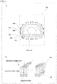
- FIG. 1 The configuration of a photodetector 100 according to a first embodiment of the present invention is now described with reference to FIG. 1 .
- a positron emission tomography apparatus (PET apparatus) 103 is described.
- the positron emission tomography apparatus 103 is an apparatus that images the inside of a subject (such as a human body) using a drug labeled with a positron-emitting radionuclide. Specifically, the positron emission tomography apparatus 103 is configured to acquire a position at which pair annihilation of the drug has occurred by detecting a pair of gamma rays (radiations) generated by the pair annihilation of electrons and positrons of the drug. Furthermore, the positron emission tomography apparatus 103 is configured to form (capture) an image of the inside of the subject by acquiring a plurality of positions at which the pair annihilation of the drug has occurred. The formed image is used for image diagnosis for determining the presence or absence of cancer cells, for example.
- the photodetector 100 used in the positron emission tomography apparatus 103 is configured to image the subject in the supine position.
- photodetectors 100 constitute a photodetector array 101 (see FIG. 1(b) ) integrated in an array.
- a plurality of photodetectors 100 surround the periphery of the subject in a state in which the plurality of photodetectors 100 are directed to the body axis (an axis that extends from the head to the legs) of the subject.
- a plurality of photodetectors 100 are disposed with the same configuration also in a direction (the rearward direction of the plane of the figure) in which the body axis of the subject extends (not shown).
- the gamma rays generated by the pair annihilation of the drug are radiations of 511 keV, and cannot be directly detected by the photodetector 100. Therefore, a scintillator array 102 is provided between the subject and the photodetector 100 (photodetector array 101).
- a scintillator array 102 is provided between the subject and the photodetector 100 (photodetector array 101).
- the photodetectors 100 are included in the photodetector array 101 and are arranged in a matrix.
- the matrix (photodetector array 101) of the photodetectors 100 has eight rows and eight columns, the total number of which is sixty-four, for example.
- the photodetector array 101 includes a multi-channel OR gate E1, a resistor matrix E2, and a position/energy acquirer E3.
- One of a plurality of photodetectors 100 corresponds to one channel, and each channel includes a large number of photoelectric conversion elements 1 (described below; see FIG. 3 ).
- two signal lines (a trigger signal line L1 and an anode signal line L2) extend from each of the photodetectors 100.
- the trigger signal line L1 which is a first signal line, transmits a trigger signal SigTrig output from each of the photodetectors 100 to the multi-channel OR gate E1.
- Each of the photodetectors 100 includes SiPMs (Silicon Photomultipliers), for example.
- portions of the signal lines indicated by thick lines are bus lines, and indicate that a plurality of signal lines extend independently of each other and along each other without being connected to each other.
- the multi-channel OR gate E1 receives the trigger signal SigTrig, which is described below, output from each of the plurality of photodetectors 100.
- the trigger signal SigTrig output from each of the photodetectors 100 is output as a single addition trigger signal SigSumTrig from the multi-channel OR gate E1.
- the resistor matrix E2 adjusts the current and/or voltage of the received anode signal SigAn output from each of the plurality of photodetectors 100, and outputs the adjusted signal to the position/energy acquirer E3.
- the position/energy acquirer E3 calculates a position at which light is detected (a position corresponding to one photodetector 100) and the total amount of detected light based on the signal output from the resistor matrix E2 (the anode signal SigAn output from each of the photodetectors 100).
- the total amount of detected light corresponds to the energy of the gamma rays incident on the scintillator array 102. Therefore, the energy of the incident gamma rays can be calculated based on the calculated total amount of light.
- a position signal SigPos related to the calculated position and an energy signal SigEn related to the total amount of light (the energy of the incident gamma rays) are output from the position/energy acquirer E3.
- the configuration of one photodetector 100 is now described with reference to FIG. 3 .
- the configurations of the plurality of photodetectors 100 are the same as each other.
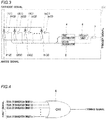
- the photodetector 100 includes the photoelectric conversion elements 1 that operate in a Geiger mode in which a voltage equal to or higher than a breakdown voltage is applied, and that output signals in response to light being incident thereon.
- the photoelectric conversion elements 1 include avalanche photodiodes (APDs), for example.
- the photoelectric conversion elements 1 are semiconductors in which a reverse bias is applied to a p-n junction, and no current flows therethrough except for a dark current under normal conditions. When photons are incident on the photoelectric conversion elements 1, electron-hole pairs are generated by the photons, and a current flows therethrough.
- the voltage that exceeds the breakdown voltage is applied such that chained generation of electron-hole pairs occurs, and thus the current increases rapidly and Geiger discharge occurs.
- the current having a good S/N ratio flows with respect to one incident photon (weak light), and thus photons can be detected with high accuracy.
- the plurality of photoelectric conversion elements 1 (photoelectric conversion elements 11, 12, 13, ..., and In: n represents the number of photoelectric conversion elements) are provided.
- the plurality of photoelectric conversion elements 1 are connected in parallel to each other.
- the photodetector 100 also includes quenching elements 2 (21 to 2n).
- the quenching elements 2 are connected in series to the plurality of photoelectric conversion elements 1, respectively.
- a voltage is generated in the corresponding quenching element 2 (one of 21 to 2n) by the current.
- the quenching element 2 reduces the voltage to be applied to the corresponding photoelectric conversion element 1 to less than the breakdown voltage.
- Geiger discharge in the photoelectric conversion element 1 is stopped. Consequently, a voltage equal to or higher than the breakdown voltage is again applied to the photoelectric conversion element 1. That is, the photoelectric conversion element 1 is returned to a state in which incidence of a photon can be detected.
- the quenching element 2 includes a resistor and/or a transistor, for example.
- the photodetector 100 also includes binarization circuits 3.
- the binarization circuits 3 are connected between the anode sides of the plurality of photoelectric conversion elements 1 and the quenching elements 2. Furthermore, each of the binarization circuits 3 is provided between each of the photoelectric conversion elements 1 and a first discriminator 4 described below, and between each of the plurality of photoelectric conversion elements 1 and a second discriminator 5 described below. That is, each of the binarization circuits 3 is provided both between each of the plurality of photoelectric conversion elements 1 and the first discriminator and between each of the plurality of photoelectric conversion elements 1 and the second discriminator. Specifically, one common binarization circuit 3 is provided between one photoelectric conversion element 1 and the first discriminator and between one photoelectric conversion element 1 and the second discriminator.
- the binarization circuits 3 When receiving voltage signals based on incidence of photons in the photoelectric conversion elements 1, the binarization circuits 3 output High (H-level, On) signal pulses. Specifically, the binarization circuits 3 are configured to output High (H-level, On) signals SigBin during a period in which the voltage signals received from the photoelectric conversion elements 1 exceed a binary threshold ThBin, and output Low (L-level, Off) signals SigBin during a period in which the voltage signals received from the photoelectric conversion elements 1 fall below the binary threshold ThBin. That is, the binarization circuits 3 output rectangular signals (pulses). Each of the binarization circuits 3 includes an inverter, for example.
- the photodetector 100 also includes the first discriminator 4 that discriminates a first signal Sig1 based on the signals output from the plurality of photoelectric conversion elements 1 using a first threshold Th1.
- the first discriminator 4 includes an OR gate that receives the first signal Sig1, which is an integration of the signals SigBin output from the plurality of binarization circuits 3 (31 to 3n). The first discriminator 4 outputs a High signal when the first signal Sig1 exceeds the first threshold Th1.
- the first threshold Th1 is set such that the first discriminator 4 outputs a High timing signal SigTim when any of the binarization circuits 3 outputs a High signal, and the first discriminator 4 outputs a Low timing signal SigTim when none of the binarization circuits 3 outputs a High signal. That is, the first discriminator 4 includes the OR gate, and thus the first discriminator 4 outputs the High timing signal SigTim during a period in which any of the signals output from the plurality of binarization circuits 3 is High, and outputs (discriminates) the Low timing signal SigTim during a period other than the above period. Therefore, the timing signal SigTim output from the first discriminator 4 is a rectangular signal (pulse).
- the photodetector 100 also includes the second discriminator 5 that discriminates a second signal Sig2 based on the signals output from the photoelectric conversion elements 1 using a second threshold Th2, which is larger than the first threshold Th1.
- the second discriminator 5 is configured to discriminate whether or not the value of the second signal Sig2, which is an integration of the signals SigBin output from the plurality of binarization circuits 3 (31 to 3n), is larger than the second threshold Th2.
- the signals SigBin output from a set of a plurality of common binarization circuits 3 (31 to 3n) are integrated and input into the first discriminator 4 and the second discriminator 5, and thus the first signal Sig1 and the second signal Sig2 are the same.
- the second discriminator 5 is configured to integrate the signals SigBin output from the plurality of binarization circuits 3 (31 to 3n), output a High level signal SigLev during a period in which the signal obtained by the integration exceeds the second threshold Th2, and output a Low level signal SigLev during a period in which the signal obtained by the integration falls below the second threshold Th2.
- the second threshold Th2 is set to a value corresponding to five High signals SigBin respectively output from the binarization circuits 3, for example.
- the second signal Sig2 exceeds the second threshold during a period in which High signals are output from the five or more binarization circuits 3 (a period in which High periods of square waves of the five or more binarization circuits 3 overlap), and thus the second discriminator 5 outputs the High level signal SigLev.
- the second signal Sig2 does not reach the second threshold during a period other than the above period, and thus the second discriminator 5 outputs the Low level signal SigLev.
- the second discriminator 5 includes a plurality of resistors 51 (511, 512, 513, ..., and 51n) so as to correspond to the plurality of binarization circuits 3 (31 to 3n).
- a voltage adder 52 adds, amplifies and outputs the binarized signals SigBin respectively input from the plurality of binarization circuits 3 (31 to 3n) via the resistors 51.
- the second discriminator 5 includes a resistor 53.
- the resistor 53 is connected in parallel to the voltage adder 52, and adjusts the degree of amplification by the voltage adder 52.
- the second discriminator 5 also includes a comparator (CMP) 54.
- the comparator 54 compares the voltage of the added signal output from the voltage adder 52 with the voltage of the second threshold Th2, outputs the High level signal SigLev when the voltage of the added signal exceeds the voltage of the second threshold Th2, and otherwise outputs the Low level signal SigLev.
- an appropriate value (a value corresponding to five to ten incident photons, for example) is set as the second threshold Th2 to discriminate between noise and a signal such that it becomes possible to discriminate between a signal due to noise and a signal due to incidence of a photon and to perform signal processing appropriately.
- the second threshold Th2 is set too large, a signal due to the scintillation light does not reach the second threshold Th2, and there is a possibility that detection of the scintillation light may be missed.
- the second threshold Th2 is set too small, signals due to a plurality of noises generated at the same time exceed the second threshold Th2, and it becomes impossible to discriminate between scintillation light and noise.
- the second threshold Th2 is set to a value corresponding to five to ten incident photons, for example.
- the second discriminator 5 does not react to the second signal Sig2 due to noise (does not output a High signal with respect to the second signal Sig2 due to noise).
- the second discriminator 5 outputs the High level signal SigLev during a period in which the second signal Sig2 exceeding the second threshold, which corresponds to incidence of a plurality of photons around the same time (consecutive incidence within a relatively short period of time), is received.
- the level signal SigLev output from the second discriminator 5 is a rectangular signal (pulse).
- the signal output from the voltage adder 52 which is an adder circuit, may have an upper limit value.
- the upper limit value needs to be larger than the second threshold Th2.
- the occurrence of noise is accidental, and thus the probability of noise occurring from the plurality of photoelectric conversion elements 1 around the same time becomes higher as the number of photoelectric conversion elements 1 included in the photodetector 100 increases. Therefore, the second threshold is set to an appropriate value in accordance with the size of the photodetector 100 (corresponding to the number of photoelectric conversion elements 1 included therein).
- the photodetector 100 is provided between the first discriminator 4 and a trigger signal generator 7 (described below), and includes a delay unit 6 configured to delay the timing signal SigTim to be transmitted from the first discriminator 4 to the trigger signal generator 7.
- the delay unit 6 is configured to delay and output the timing signal SigTim input from the first discriminator 4. Consequently, the delay unit 6 outputs a delay timing signal SigDelTim obtained by delaying the timing at which the timing signal SigTim is switched between High and Low. At this time, the delay timing signal SigDelTim is output with a slight delay (several nanoseconds to several tens of nanoseconds, for example) from output of the level signal SigLev. The details are described below based on a timing chart in FIG. 7 .
- the delay unit 6 includes a delay circuit, for example.
- the photodetector 100 includes the trigger signal generator 7 that generates the trigger signal SigTrig indicating that light to be detected is incident when the first discriminator 4 discriminates that the first signal Sig1 is larger than the first threshold Th1 and the second discriminator 5 discriminates that the second signal Sig2 is larger than the second threshold Th2.
- the trigger signal generator 7 includes an AND gate.
- the trigger signal generator 7 receives the delay timing signal SigDelTim obtained by delaying the timing signal SigTim output from the first discriminator 4 by the delay unit 6 and the level signal SigLev output from the second discriminator 5.
- the trigger signal generator 7 is configured to generate a High trigger signal SigTrig during a period in which both the delay timing signal SigDelTim and the level signal SigLev are High, and to generate a Low trigger signal SigTrig during a period other than the above period. Then, the trigger signal SigTrig generated by the trigger signal generator is output to the multi-channel OR gate E1 (see FIG. 2 ).
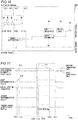
- FIG. 7 shows the signals output from the respective locations in the photodetector 100 along a time axis.
- the left side of the chart shows the locations from which the signals are output.
- the top of the chart shows the light (signal) incident on the photodetector 100.
- a pulse P1 (triangular pulse) is output from the photoelectric conversion element 11 due to noise such as dark current.
- the magnitude of the pulse P1 becomes larger than the binary threshold ThBin of the binarization circuit 3, and thus a High rectangular pulse R1 is output from the binarization circuit 3.
- the High rectangular pulse R1 is input into the first discriminator 4.
- the first discriminator 4 includes the OR gate (that is, the first threshold Th1 of the first discriminator 4 has the same value as the binary threshold ThBin), and thus during the period from the time T1 to the time T2, the first discriminator 4 outputs the High rectangular pulse.
- the occurrence of noise such as dark current is sporadic, and thus the possibility of a plurality of (consecutive) occurrences around the same time is low. Therefore, the first signal Sig1 (second signal Sig2) input into the second discriminator 5 is not added (or is relatively small even if it is added), and thus the second signal Sig2 does not exceed the second threshold Th2. That is, the second discriminator 5 outputs a Low signal.
- pulses P2, P3, ... are respectively output from a plurality of photoelectric conversion elements 1 of the photoelectric conversion elements 11, 12, ..., and In.
- the outputs of the plurality of pulses P2, P3, ... occur consecutively.
- the first signal Sig1 input into the first discriminator 4 exceeds the first threshold Th1, and thus the timing signal SigTim indicating the incident timing of a photon becomes High.
- the second signal Sig2 of the second discriminator 5 is smaller than the second threshold Th2, and thus the second discriminator 5 outputs a Low level signal SigLev.
- the pulses P3, ... are consecutively output such that at a time T4, the second signal Sig2 of the second discriminator 5 exceeds the second threshold.
- the level signal SigLev output from the second discriminator 5 becomes High.
- the light incidence peaks, and then the light incidence gradually decreases.
- the second signal Sig2 of the second discriminator 5 falls below the second threshold Th2, and thus the level signal SigLev output from the second discriminator 5 becomes Low.
- the first signal Sig1 input into the first discriminator 4 disappears (falls below the first threshold Th1), and thus the timing signal SigTim output from the first discriminator 4 becomes Low.
- the timing signal SigTim output from the first discriminator 4 is input into the delay unit 6.
- the delay unit 6 outputs the delay timing signal SigDelTim obtained by delaying the timing signal SigTim.
- the timing signal SigTim a High signal is output when one photon is incident. Therefore, the time taken for a signal to rise corresponds to the time from photon incidence to current generation, and is determined to be a substantially constant value.
- the level signal SigLev a High signal is output when five photons are consecutively incident. However, the time from incidence of the first photon to incidence of the fifth photon through incidence of the second, third, and fourth photons varies, and thus the time taken for a signal to rise lengthens and becomes a relatively uncertain value. Therefore, the delay unit 6 delays the timing signal SigTim with respect to the level signal SigLev.
- the rising timing (time T5) of the delay timing signal SigDelTim is later than the rising timing (time T4) of the level signal SigLev.
- time T5 of the delay timing signal SigDelTim is later than the rising timing (time T4) of the level signal SigLev.
- the trigger signal generator 7 generates the trigger signal SigTrig, which is the logical conjunction of the delay timing signal SigDelTim and the level signal SigLev.
- the trigger signal SigTrig becomes High.
- the trigger signal SigTrig becomes Low.
- the trigger signal SigTrig becomes High (On) only when scintillation light is incident on the plurality of photoelectric conversion elements 1 (when the level signal SigLev is High).
- the rising timing of the trigger signal SigTrig is aligned with the rising timing of the delay timing signal SigDelTim at the time T5.
- the delay time (delay circuit delay time), which is a substantially constant value, of the delay timing signal SigDelTim from the timing signal SigTim, and the delay time (propagation delay time), which is a substantially constant value, due to subsequent stage circuits are measured in advance.
- the known delay time is subtracted from the time at which the trigger signal SigTrig becomes High such that the rising (High) timing of the trigger signal SigTrig can be aligned with the rising timing of the timing signal SigTim. That is, the time at which a photon is first incident on the photodetector 100 can be acquired (calculated) substantially accurately.
- the high accuracy of generation of the trigger signal SigTrig can be obtained from a simple readout circuit.
- the photoelectric conversion element 1 constitutes an unintended pseudo capacitor (parasitic capacitance). Therefore, with respect to the anode signal SigAn of the photodetector 100, the parasitic capacitance and the subsequent stage circuits (the resistor matrix E2 and the position/energy acquirer E3) constitute an unintended low-pass filter (LPF). Furthermore, the parasitic capacitance of another photodetector 100 also affects the low-pass filter, and thus when the number of photodetectors 100 increases, the high-frequency component of a signal significantly disappears, and the signal is deteriorated.
- LPF unintended low-pass filter
- the trigger signal SigTrig is generated in the photodetector 100 (is isolated from another photodetector 100), and thus the influence of the parasitic capacitance of another photodetector 100 and the influence of noise generated from another photodetector 100 can be reduced.
- the signals of the photoelectric conversion elements 1 are input into the first discriminator 4 and the second discriminator 5 through the binarization circuits 3, and thus the trigger signal SigTrig can reduce the influence of the parasitic capacitance of each of the photoelectric conversion elements 1 also in the photodetector 100.
- the positron emission tomography apparatus 103 can accurately acquire the position at which the pair annihilation of the drug has occurred.
- a graph in FIG. 8 shows the results of a simulation in which the probability of detection when a plurality of photons are incident on the photodetector 100 is 40% per photon.
- the horizontal axis of the graph represents values obtained by converting the magnitude of the threshold at which the trigger is High into the number of detected photons.
- the vertical axis of the graph represents values obtained by converting the full width at half maximum of the jitter of the trigger signal into the number of incident photons, and corresponds to the variation in the number of detected photons.
- the detection timing of one photon is acquired using the first threshold Th1 corresponding to the detection of the photon with high trigger accuracy, and thus information about the timing at which the photon is incident can be accurately obtained.
- the time at which the gamma ray is incident can be accurately detected.
- the photodetector 100 includes the trigger signal generator 7 configured to generate the trigger signal SigTrig indicating that the light to be detected is incident when the first discriminator 4 discriminates that the first signal Sig1 is larger than the first threshold Th1 and the second discriminator 5 discriminates that the second signal Sig2 is larger than the second threshold Th2. Accordingly, the signal output from the photoelectric conversion elements 1 using the relatively large second threshold Th2 is discriminated such that false detection caused by noise (relatively small signal) can be significantly reduced or prevented. Furthermore, the timing at which it is discriminated that the first signal Sig1 is larger than the first threshold Th1 substantially accurately reflects the time at which the light is incident.
- the trigger signal SigTrig indicating that the light to be detected is incident is generated based on the timing signal SigTrig from the first discriminator 4 and the level signal SigLev from the second discriminator 5 such that the precise time at which the light is incident can be accurately detected while false detection is significantly reduced or prevented.
- the photodetector 100 includes the delay unit 6 configured to delay the timing signal SigTrig to be transmitted from the first discriminator 4 to the trigger signal generator 7 between the first discriminator 4 and the trigger signal generator 7.
- the second threshold Th2 is larger than the first threshold Th1, and thus the time taken for the second signal Sig2 based on the signal output from the photoelectric conversion elements 1 to reach the second threshold Th2 is longer than the time taken for the first signal Sig1 output from the photoelectric conversion elements 1 to reach the first threshold Th1 (the time for the second signal Sig2 based on the signal output from the photoelectric conversion elements 1 to reach the second threshold Th2 is later than the time for the first signal Sig1 output from the photoelectric conversion elements 1 to reach the first threshold Th1).
- the delay unit 6 configured to delay the timing signal SigTrig to be transmitted from the first discriminator 4 to the trigger signal generator 7 is provided between the first discriminator 4 and the trigger signal generator 7 such that the timing at which the first signal Sig1 becomes High can be later than the timing at which the second signal Sig2 becomes High. Consequently, it is possible to more accurately achieve both detection of the precise time at which the light is incident and significant reduction in or prevention of false detection.
- the second discriminator 5 is configured to discriminate whether or not the value of the second signal Sig2, which is a signal obtained by adding the first signal Sig1 output from the plurality of photoelectric conversion elements 1, is larger than the second threshold Th2.
- the first signal Sig1 includes a signal corresponding to incidence of one photon or a signal due to noise.
- a plurality of photons are incident around the same time. Accordingly, a plurality of first signals Sig1 are (consecutively) generated around the same time, and thus the second signal Sig2 is consecutively increased.
- the second signal Sig2 is a signal obtained by adding the first signal Sig1 output from the plurality of photoelectric conversion elements 1, is larger than the second threshold Th2 such that incidence of light can be accurately detected.
- the photodetector 100 includes the binarization circuit 3 provided in at least a region between each of the plurality of photoelectric conversion elements 1 and the first discriminator 4 among the region between each of the plurality of photoelectric conversion elements 1 and the first discriminator 4 and a region between each of the plurality of photoelectric conversion elements 1 and the second discriminator 5 and configured to binarize the signal output from each of the plurality of photoelectric conversion elements 1.
- the binarized signal SigBin which is a binarized signal (digital signal)
- the binarization circuit 3 is provided in at least the region between each of the plurality of photoelectric conversion elements 1 and the first discriminator 4 such that the processing time taken to detect incidence of light can be reduced.
- the common binarization circuit 3 is provided both between each of the plurality of photoelectric conversion elements 1 and the first discriminator 4 and between each of the plurality of photoelectric conversion elements 1 and the second discriminator. Accordingly, as compared with the case in which the binarization circuit 3 is provided only between each of the plurality of photoelectric conversion elements 1 and the first discriminator 4, the processing time taken to detect incidence of light can be further reduced.
- the photodetector 100 is used in the positron emission tomography apparatus (PET apparatus) 101. Accordingly, the precise time at which the light based on the gamma rays emitted due to the electron-positron pair annihilation is incident can be more accurately detected.
- PET apparatus positron emission tomography apparatus
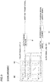
- the photodetector 200 does not include binarization circuits 3 unlike the aforementioned first embodiment. Furthermore, in the second embodiment, the photodetector 200 includes a signal duplicator 8 unlike the aforementioned first embodiment.
- the same configurations as those of the first embodiment are denoted by the same reference numerals, and description thereof is omitted.
- photodetectors 200 are arranged in a matrix (eight rows and eight columns), and include a multi-channel OR gate E1, a resistor matrix E2, and a position/energy acquirer E3, as in the first embodiment.
- a detection signal (slow signal SigSlow) output from the photodetector 200 is input into the resistor matrix E2 via a slow signal line L20.
- the slow signal SigSlow is a signal obtained by duplicating an anode signal SigAn by the signal duplicator 8 (described below; see FIG. 10 ).
- the photodetector 200 includes a plurality of photoelectric conversion elements 1, a plurality of quenching elements 2 (21 to 2n) respectively connected in series to the photoelectric conversion elements 1 (11 to 1n), the signal duplicator 8, a first discriminator 40, a second discriminator 50, and a trigger signal generator 70.
- the first discriminator 40 and the second discriminator 50 are configured to discriminate a first signal Sig11 and a second signal Sig12 of analog signals output from the signal duplicator 8.
- the signal duplicator 8 is provided in common between the photoelectric conversion elements 1 and each of the first discriminator 40 and the second discriminator 50, and duplicates the same signal as the anode signal SigAn output from the photoelectric conversion elements 1.
- the photodetector 200 is configured to acquire the position of a photoelectric conversion element 1 on which light is incident and the total amount of light incident on the photoelectric conversion element 1 with the slow signal SigSlow duplicated by the signal duplicator 8.
- the signal duplicator 8 outputs the first signal Sig11 to the first discriminator 40, outputs the second signal Sig12 to the second discriminator 50, and outputs the slow signal SigSlow to the resistor matrix E2.
- the first signal Sig11, the second signal Sig12, and the slow signal SigSlow are the same signals obtained by duplicating the anode signal SigAn, which is an integration of signals output from the photoelectric conversion elements 1.
- the signal duplicator 8 duplicates and outputs the signals (anode signal SigAn) output from the photoelectric conversion elements such that the parasitic capacitance of the photoelectric conversion element In is insulated from the subsequent stage circuits (the resistor matrix E2 and the position/energy acquirer E3), and formation of a low-pass filter constituted by the parasitic capacitance of the photoelectric conversion element In and the subsequent stage circuits can be prevented.
- the duplicate signal is similarly insulated from the photoelectric conversion elements In of another photodetector 200, and thus it is not affected by the parasitic capacitance of the photoelectric conversion element In of another photodetector 200. Consequently, the interaction with another photodetector 200 can be reduced, and signal deterioration can be significantly reduced or prevented.
- anode signals SigAn output from the (plurality of) photodetectors 200 are directly used to acquire the energy and position without providing the signal duplicator 8
- the anode signals SigAn are affected by the parasitic capacitances (unintended formation of capacitors) of the photoelectric conversion elements 1 of the photodetectors 200 themselves, and the anode signals SigAn are deteriorated (the high frequency components are blurred).
- the signals output to generate a trigger signal SigTrig (the signals respectively output to the first discriminator 40 and the second discriminator 50) are also affected by the similar deterioration, and thus the trigger signal SigTrig finally output from the trigger signal generator 70 is also deteriorated.
- the anode signal SigAn is directly used in the trigger signal generator 70 (because the input impedance of a circuit of the trigger signal generator 70 is not 0), the signal is similarly affected and deteriorated by the parasitic capacitance of the photoelectric conversion element In.
- the signal duplicator 8 duplicates the anode signal SigAn output from the anode sides of the photoelectric conversion elements 1, and outputs signals equivalent to the anode signal SigAn to a signal line connected to the resistor matrix E2 (see FIG. 9 ), a signal line connected to the first discriminator 40, and a signal line connected to the second discriminator 50, respectively.
- the signal output to the resistor matrix E2 is the slow signal SigSlow.
- the position/energy acquirer E3 calculates the position of the photodetector 200 that has detected the light and the total amount of the detected light (the energy of the incident gamma rays) based on the signal output from the resistor matrix E2 (the slow signal SigSlow output from each of the photodetectors 200). Then, a signal related to the calculated position and a signal related to the energy are output from the position/energy acquirer E3.
- the signals output to the first discriminator 40 and the second discriminator 50 are used to generate the trigger signal SigTrig.
- Two duplicate signals respectively output from the signal duplicator 8 to the first discriminator 40 and the second discriminator 50 in order to generate the trigger signal SigTrig and duplicate signals output to the subsequent stage circuits in order to acquire the position and energy are insulated from the parasitic capacitance of the photoelectric conversion element In and an unintended low-pass filter (LPF) formed by the photoelectric conversion element In, the subsequent stage circuits, and another photodetector 200.
- LPF unintended low-pass filter
- the signals duplicated and insulated by the signal duplicator 8 are used to significantly reduce or prevent the influences of the parasitic capacitance and the low-pass filter on the trigger signal SigTrig and the slow signal SigSlow (deterioration of the trigger signal SigTrig and the slow signal SigSlow due to the parasitic capacitance and the low-pass filter). Furthermore, the trigger signal SigTrig and the slow signal SigSlow are insulated from each other, and thus interaction of the trigger signal SigTrig and the slow signal SigSlow with each other can be significantly reduced or prevented.
- the influences that appear on the signals are minor due to the binarized trigger signals SigTrig (due to the trigger signals SigTrig multiple-insulated from the photoelectric conversion elements In of the photodetectors 200), and thus there is no problem.
- the signal duplicator 8 drives the subsequent stage circuits (the multi-channel OR gate E1, the resistor matrix E2, and the position/energy acquirer E3), and thus even with the slow signals SigSlow of the plurality of photodetectors 200 connected to each other (even with the merged slow signals SigSlow), the influences are minor such that there is no problem.
- a terminal that outputs the anode signal SigAn not directly used for measurement is connected to a low impedance power supply or a ground potential (ground: GND) such that the terminal that outputs the anode signal SigAn does not form a low-pass filter due to the influence of the parasitic capacitance.
- GND ground potential
- the first discriminator 40 outputs a High timing signal SigTim during a period in which the input first signal Sig11 exceeds a first threshold Th1, and outputs a Low timing signal SigTim during a period in which the input first signal Sig11 falls below the first threshold Th1.
- the second discriminator 50 outputs a High level signal SigLev during a period in which the input second signal Sig12 exceeds a second threshold Th2, and outputs a Low level signal SigLev during a period in which the input second signal Sig12 falls below the second threshold Th2.
- a delay unit 60 delays the timing signal SigTim output from the first discriminator 40, and outputs a delay timing signal SigDelTim.
- the rising timing (the timing at which the delay timing signal SigDelTim becomes High) of the delay timing signal SigDelTim is later than the rising timing of the level signal SigLev.
- the trigger signal generator 70 outputs a High trigger signal SigTrig when both the input delay timing signal SigDelTim and the input level signal SigLev become High, and otherwise outputs a Low trigger signal SigTrig.
- one pulse P0 corresponding to the signal of one photoelectric conversion element 1 is output from the photoelectric conversion element 1 to the signal duplicator 8, and the signal of the pulse P0 duplicated by the signal duplicator 8 is input into the first discriminator 40 and the second discriminator 50. That is, it is assumed that a signal corresponding to the signal of one photoelectric conversion element 1 (a duplicate signal of the pulse P0) is input as the first signal Sig11 into the first discriminator 40.
- the first signal Sig11 (the duplicate signal of the pulse P0) is larger than the first threshold Th1 of the first discriminator 40 during a period from a time T21 to a time T22, and thus the first discriminator 40 outputs a High timing signal SigTim, which is a rectangular pulse R0.
- a signal corresponding to the signal of one photoelectric conversion element 1 (a duplicate signal of the pulse P0) is similarly input as the second signal Sig12 into the second discriminator 50.
- the second signal Sig12 (the duplicate signal of the pulse P0) input into the second discriminator 50 does not exceed the second threshold Th2 corresponding to the case in which a plurality of pulses are added. That is, the second discriminator 50 does not output a High level signal SigLev, but outputs a Low level signal SigLev.
- the second signal Sig12 (first signal Sig11) becomes relatively large. Specifically, first, at a time T23, the first signal Sig11 input into the first discriminator 40 exceeds the first threshold Th1, and thus the timing signal SigTim indicating the incident timing of a photon becomes High. At this point of time, the second signal Sig12 of the second discriminator 50 is smaller than the second threshold Th2, and thus the second discriminator 5 outputs a Low level signal SigLev.
- the second signal Sig12 of the second discriminator 50 exceeds the second threshold Th2.
- the level signal SigLev output from the second discriminator 50 becomes High.
- the light incidence peaks, and then the light incidence gradually decreases.
- the second signal Sig12 of the second discriminator 50 falls below the second threshold Th2, and thus the level signal SigLev output from the second discriminator 50 becomes Low.
- the first signal Sig11 input into the first discriminator 40 disappears (falls below the first threshold Th1), and thus the timing signal SigTim output from the first discriminator 40 becomes Low.
- the timing signal SigTim output from the first discriminator 40 is input into the delay unit 60.
- the delay unit 60 outputs the delay timing signal SigDelTim obtained by delaying the timing signal SigTim.
- the trigger signal generator 70 generates the trigger signal SigTrig, which is the logical conjunction of the delay timing signal SigDelTim and the level signal SigLev.
- the trigger signal SigTrig becomes High.
- the trigger signal SigTrig becomes Low.
- the trigger signal SigTrig is aligned with the delay timing signal SigDelTrig, the rising timing of which reflects the precise incidence time of the photon.
- the trigger signal SigTrig becomes High when the level signal SigLev not indicating noise but indicating incidence of the photon is High.
- the first discriminator 40 and the second discriminator 50 are configured to discriminate the first signal Sig11 and the second signal Sig12 of analog signals. Accordingly, it is not necessary to separately provide a circuit for digitizing (binarizing) the signals output from the photoelectric conversion elements 1, and thus the device configuration of the photodetector 200 can be simplified.
- the photodetector 200 includes the signal duplicator 8 provided between the photoelectric conversion elements 1 and each of the first discriminator 40 and the second discriminator 50 and configured to duplicate the same signal as the anode signal SigAn output from the photoelectric conversion elements 1. Furthermore, the position of the photoelectric conversion element 1 on which light is incident and the total amount of light incident on the photoelectric conversion element 1 are acquired with the slow signal SigSlow duplicated by the signal duplicator 8.
- the parasitic capacitance of the photoelectric conversion element 1, the subsequent stage circuits, another photodetector 200, etc. constitute an unintended low-pass filter (LPF), and thus the signal output to the outside of one photodetector 200 may be deteriorated.
- LPF unintended low-pass filter
- At least one of the position of the photoelectric conversion element 1 on which light is incident and the total amount of light incident on the photoelectric conversion element 1 is acquired with the slow signal SigSlow duplicated by the signal duplicator 8 and insulated from the parasitic capacitance of the photoelectric conversion element 1 and the low-pass filter (LPF) formed by the subsequent stage circuits, another photodetector 200, etc. such that the position of the photoelectric conversion element 1 on which light is incident and the total amount of light incident on the photoelectric conversion element 1 can be acquired while the deterioration of the signal is significantly reduced or prevented. That is, the position of the photoelectric conversion element 1 on which light is incident and the total amount of light incident on the photoelectric conversion element 1 (the energy of the incident gamma rays) can be accurately acquired.
- the slow signal SigSlow duplicated by the signal duplicator 8 and insulated from the parasitic capacitance of the photoelectric conversion element 1 and the low-pass filter (LPF) formed by the subsequent stage circuits, another photodetector 200
- FIG. 12 The configuration of a photodetector 300 according to a third embodiment of the present invention is now described with reference to FIG. 12 .
- the same configurations as those of the first embodiment are denoted by the same reference numerals, and description thereof is omitted.
- photodetector elements 301 are arranged in a matrix of 1 rows and m columns. Therefore, in order to indicate the position of each of the photodetector elements 301 in an X direction, any of numbers 0, 1, 2, ..., and 1-1 is given, and in order to indicate the position in a Y direction, any of numbers 0, 1, 2, ..., and m-1 is given.
- the photodetector 300 includes four photodetector elements 301 each corresponding to one channel provided with a set of a plurality of photoelectric conversion elements 1, quenching elements 2 respectively connected in series to the plurality of photoelectric conversion elements 1, a first discriminator 4, a second discriminator 5, a delay unit 6, and a trigger signal generator 7.
- one photodetector element 301 is configured to be equivalent to one photodetector 100 according to the first embodiment, for example. As shown in FIG.
- the photodetector 300 further includes a resistor matrix E20 (not shown) that receives an anode signal SigAn output from each photodetector element 301 corresponding to the channel and indicating the position of the photoelectric conversion element 1 on which light is incident and the total amount of light incident on the photoelectric conversion element 1, and a multi-channel OR gate E10 (not shown) that receives a trigger signal SigTrig output from each photodetector element 301 corresponding to the channel.
- the multi-channel OR gate E10 is an example of an "OR gate" in the claims.
- the configuration of the photodetector 300 corresponding to a group of the above four (two rows and two columns) photodetector elements 301 is also applied to the other photodetector elements 301 individually (every four photodetector elements 301).
- the photodetector elements 301 are grouped in small units of four photodetector elements 301, and thus the processing load on the subsequent stage circuits (circuits that calculate the light incident timing, the total amount of light, and the light incident position, for example) is reduced.
- the photodetector 300 may include a position/energy acquirer (not shown) that receives each of the above signals SigA to SigD output from the resistor matrix E20 of each of a plurality of photodetectors 300, and outputs a position signal indicating (specifying) the photodetector element 301 on which light is incident and an energy signal indicating the total amount of light incident on the photodetector element 301 (the energy of the incident gamma rays).
- a position/energy acquirer not shown
- the photodetector 300 includes the plurality of photodetector elements 301 each corresponding to the channel including a set of the photoelectric conversion elements 1, the first discriminator 4, the second discriminator 5, and the trigger signal generator 7, and further includes the multi-channel OR gate E10 (OR gate) that receives the trigger signal SigTrig output from each photodetector element 301 corresponding to the channel and the resistor matrix E20 that receives the anode signal SigAn output from each photodetector element 301 corresponding to the channel and indicating the position of the photoelectric conversion element 1 on which light is incident and the total amount of light incident on the photoelectric conversion element 1 (the energy of the incident gamma rays).
- OR gate OR gate
- the trigger signal SigTrig output from each channel and the anode signal SigAn indicating at least one of the position and the energy can be merged, and thus the processing load on the subsequent stage circuits (circuits that calculate the light incident timing, the total amount of light, and the light incident position, for example) can be reduced.
- the delay unit 6 may be provided inside the first discriminator 4.
- the present invention is not limited to this.
- the number of photodetectors 100 (200, 300) may be other than sixty-four, or the photodetectors 100 (200) may be arranged in a state (such as one row) other than a matrix.
- the present invention is not limited to this.
- the number of photodetectors 100 (200) and the number of scintillator elements S, which are relative to each other may be any numbers (the scintillator elements S in four rows and four columns are provided for the photodetectors 100 (200) in three rows and three columns, for example).
- one scintillator element S may be provided for one photodetector 100. Furthermore, one scintillator element S may be provided for the entire photodetector array 101 including the photodetectors 100 (200). In addition, there may not be a fixed correspondence in number between the photodetectors 100 (200) and the scintillator elements S.
- the delay time for the timing signal SigTim by the delay unit 6 (60) is set to a constant value in each of the aforementioned first and second embodiments, the present invention is not limited to this.
- the delay time may be adjusted for each photodetector 100 (200) .
- the present invention is not limited to this.
- the first threshold Th1 may be adjusted to a value corresponding to signals indicating incidence of any number of photons other than one photon.
- the present invention is not limited to this.
- the first threshold Th1 may be adjusted to a value corresponding to signals indicating incidence of any number of photons other than five to ten photons.
- first threshold Th1 and the second threshold Th2 are set to the same values across all the photodetectors 100 (200)
- the present invention is not limited to this.
- the first threshold Th1 and the second threshold Th2 may be adjusted for each photodetector 100 (200).
- the first discriminator 4 (40) includes an OR gate
- the present invention is not limited to this.
- the first discriminator 4 (40) may include a voltage adder 52 or the like, similarly to the second discriminator 5 (50).
- the OR gate is more advantageous in terms of circuit response speed and circuit miniaturization.
- the present invention is not limited to this.
- the position and the energy may be acquired from the length of the time during which the signal exceeds the corresponding threshold and a time difference based on the signal output from the first discriminator 4 (40) or the second discriminator 5 (50).
- the position and the energy may be acquired based on a cathode signal output from the cathode sides of the photoelectric conversion elements 1.
- the multi-channel OR gate E1, the resistor matrix E2, and the position/energy acquirer E3 may be connected to the cathode signal side.
- the quenching elements 2 connected to the photoelectric conversion elements, the binarization circuits 3, the first discriminator 4 (40), the second discriminator 5 (50), the delay unit 6 (60), the trigger signal generator 7 (70), and the circuit contributing to generation of the trigger signal SigTrig, such as the signal duplicator 8, are similarly connected to the cathode sides of the photoelectric conversion elements 1.
- a second discriminator 150 may include switches 55, current sources 56, a current-voltage converter 57, and a comparator 58 as shown in FIG. 13 .
- the switches 55 are a group of switches respectively connected to binarization circuits 3 or photoelectric conversion elements 1, and turn on when light is detected in the corresponding photoelectric conversion elements 1, and send current signals.
- the current-voltage converter 57 converts the current signals output from the photoelectric conversion elements 1 into voltage signals.
- the comparator 58 outputs a High level signal SigLev only when a voltage exceeding a second threshold Th2 is input.
- the photodetector 100 (200) may be used to detect light in a gamma camera, spectroscopic analysis, inspection of manufactured components, a distance measuring device, and another measurement/exploration.
- a binarization circuit 3A may be provided only between each of photoelectric conversion elements 1 and a first discriminator 4.
- a signal is slightly delayed in the process of binarizing the signal by the binarization circuit 3.
- a binarization circuit 3B may be provided only between each of photoelectric conversion elements 1 and a second discriminator 5.
- separate binarization circuits 3C and 3D may be respectively provided between each of photoelectric conversion elements 1 and a second discriminator 5 and between each of the photoelectric conversion elements 1 and a second discriminator 5.
- a first signal and a second signal are different from each other unlike the case in which the common binarization circuit 3 is provided between each of the photoelectric conversion elements 1 and the second discriminator 5 and between each of the photoelectric conversion elements 1 and the second discriminator 5, to which a signal SigBin output from the same binarization circuit 3 is input.
- the present invention is not limited to this.
- a unit by which the trigger signals SigTrig and the anode signal SigAn are merged may not be four.
- grouping of the photodetector elements 301 is not limited to grouping in a matrix, but the photodetector elements 301 may be grouped one-dimensionally in each column or row.
- one photodetector element 301 is configured to be equivalent to one photodetector 100 according to the first embodiment
- the present invention is not limited to this.
- one photodetector element 301 may be configured to be equivalent to one photodetector 200 according to the second embodiment.
Landscapes
- Health & Medical Sciences (AREA)
- Life Sciences & Earth Sciences (AREA)
- Physics & Mathematics (AREA)
- High Energy & Nuclear Physics (AREA)
- Molecular Biology (AREA)
- General Physics & Mathematics (AREA)
- Spectroscopy & Molecular Physics (AREA)
- Engineering & Computer Science (AREA)
- Medical Informatics (AREA)
- Nuclear Medicine, Radiotherapy & Molecular Imaging (AREA)
- Optics & Photonics (AREA)
- Biomedical Technology (AREA)
- General Health & Medical Sciences (AREA)
- Surgery (AREA)
- Biophysics (AREA)
- Pathology (AREA)
- Radiology & Medical Imaging (AREA)
- Heart & Thoracic Surgery (AREA)
- Animal Behavior & Ethology (AREA)
- Public Health (AREA)
- Veterinary Medicine (AREA)
- Microelectronics & Electronic Packaging (AREA)
- Measurement Of Radiation (AREA)
- Nuclear Medicine (AREA)
- Light Receiving Elements (AREA)
- Photometry And Measurement Of Optical Pulse Characteristics (AREA)
Abstract
Description
- The present invention relates to a photodetector, and more particularly, it relates to a photodetector including photoelectric conversion elements that operate in a Geiger mode.
- Conventionally, a photodetector including photoelectric conversion elements that operate in a Geiger mode is known. Such a photodetector is disclosed in Japanese Patent Laid-Open No.
2012-60012 - Japanese Patent Laid-Open No.
2012-60012 - Patent Document 1: Japanese Patent Laid-Open No.
2012-60012 - However, in the photodetector disclosed in Japanese Patent Laid-Open No.
2012-60012 2012-60012 - The present invention is intended tosolve at least one of the above problems. The present invention aims to provide a photodetector capable of accurately detecting the precise time at which light is incident while significantly reducing or preventing false detection.
- In order to attain the aforementioned object, a photodetector according to an aspect of the present invention includes a plurality of photoelectric conversion elements configured to operate in a Geiger mode in which a voltage equal to or higher than a breakdown voltage is applied, and to output signals in response to light being incident thereon, a first discriminator configured to discriminate, using a first threshold, a first signal based on the signals output from the plurality of photoelectric conversion elements, a second discriminator configured to discriminate, using a second threshold larger than the first threshold, a second signal based on the signals output from the plurality of photoelectric conversion elements, and a trigger signal generator configured to generate a trigger signal, the trigger signal indicating that light to be detected is incident, the trigger signal being output when the first signal larger than the first threshold is input into the first discriminator and the second signal larger than the second threshold is input into the second discriminator.
- In the photodetector according to this aspect of the present invention, as described above, the photodetector includes the trigger signal generator configured to generate the trigger signal indicating that the light to be detected is incident when the first discriminator discriminates that the first signal is larger than the first threshold and the second discriminator discriminates that the second signal is larger than the second threshold. Accordingly, the signal output from the photoelectric conversion elements based on the relatively large second threshold is discriminated such that false detection caused by noise (relatively small signal) can be significantly reduced or prevented. Furthermore, the timing at which it is discriminated that the first signal is larger than the first threshold substantially accurately reflects the time at which a photon is incident. Consequently, the trigger signal indicating that the light to be detected is incident is generated based on the signal from the first discriminator and the signal from the second discriminator such that the precise time at which the light is incident can be accurately detected while false detection is significantly reduced or prevented.
- The aforementioned photodetector according to this aspect preferably further includes a delay unit provided between the first discriminator and the trigger signal generator, the delay unit being configured to delay a signal to be transmitted from the first discriminator to the trigger signal generator. The second threshold is larger than the first threshold, and thus the time taken for the second signal based on the signal output from the photoelectric conversion elements to reach the second threshold is longer than the time taken for the first signal output from the photoelectric conversion elements to reach the first threshold (the time for the second signal based on the signal output from the photoelectric conversion elements to reach the second threshold is later than the time for the first signal output from the photoelectric conversion elements to reach the first threshold). Therefore, the delay unit configured to delay the signal to be transmitted from the first discriminator to the trigger signal generator is provided between the first discriminator and the trigger signal generator such that the timing at which the first signal becomes High (H-level) can be later than the timing at which the second signal becomes High (H-level). Consequently, it is possible to more accurately achieve both detection of the precise time at which the light is incident and significant reduction in or prevention of false detection.
- In the aforementioned photodetector according to this aspect, the second discriminator is preferably configured to discriminate whether or not a value of the second signal, which is a signal obtained by adding the first signal output from the plurality of photoelectric conversion elements, is larger than the second threshold. The first signal includes a signal corresponding to incidence of one photon or a weak signal due to noise. When photons are actually incident on the photodetector, a plurality of photons are incident around the same time. Accordingly, a plurality of first signals are (consecutively) generated around the same time, and thus the second signal is consecutively increased. On the other hand, noise occurs sporadically in the plurality of photoelectric conversion elements, and thus the second signal remains relatively small. Therefore, it is discriminated whether or not the value of the second signal, which is a signal obtained by adding the first signal output from the plurality of photoelectric conversion elements, is larger than the second threshold such that incidence of light can be accurately detected.
- The aforementioned photodetector according to this aspect preferably further includes a binarization circuit provided in at least one of a region between each of the plurality of photoelectric conversion elements and the first discriminator and a region between each of the plurality of photoelectric conversion elements and the second discriminator, the binarization circuit being configured to binarize the signals output from the plurality of photoelectric conversion elements. The binarized signal (digital signal) has a relatively small processing load as compared with an unbinarized signal (analog signal). Therefore, the binarization circuit is provided in at least one of the region between each of the plurality of photoelectric conversion elements and the first discriminator and the region between each of the plurality of photoelectric conversion elements and the second discriminator such that the processing time taken to detect incidence of light can be reduced.
- In this embodiment, the binarization circuit is preferably provided both between each of the plurality of photoelectric conversion elements and the first discriminator and between each of the plurality of photoelectric conversion elements and the second discriminator. According to this configuration, as compared with the case in which the binarization circuit is provided only between each of the plurality of photoelectric conversion elements and the first discriminator, the processing time taken to detect incidence of light can be further reduced.
- In the aforementioned photodetector according to this aspect, the first discriminator and the second discriminator are preferably configured to discriminate the first signal and the second signal each including an analog signal. According to this configuration, it is not necessary to separately provide a circuit for digitizing (binarizing) the signals output from the photoelectric conversion elements, and thus the device configuration of the photodetector can be simplified.
- In this embodiment, the photodetector preferably further includes a signal duplicator provided between the photoelectric conversion elements and each of the first discriminator and the second discriminator, the signal duplicator being configured to duplicate a signal same as the signals to be transmitted to the first discriminator and the second discriminator, and a signal indicting at least one of a position of each of the photoelectric conversion elements on which the light is incident and a total amount of the light incident on each of the photoelectric conversion elements (a value corresponding to the energy of incident gamma rays) is preferably sent with the signal duplicated by the signal duplicator. When at least one of the position of each of the photoelectric conversion elements on which the light is incident and the total amount of the light incident on each of the photoelectric conversion elements is acquired with a signal output to the outside of one of a plurality of photodetectors, the parasitic capacitance of each of the photoelectric conversion elements, the subsequent stage circuits, another photodetector, etc. constitute an unintended low-pass filter (LPF), and thus the signal output to the outside of one photodetector may be deteriorated. Therefore, at least one of the position of each of the photoelectric conversion elements on which the light is incident and the total amount of the light incident on each of the photoelectric conversion elements is insulated from another photodetector and acquired with the signal duplicated by the signal duplicator and insulated from the parasitic capacitance of each of the photoelectric conversion elements and the low-pass filter (LPF) formed by the subsequent stage circuits, another photodetector, etc. such that the position of each of the photoelectric conversion elements on which the light is incident and the total amount of the light incident on each of the photoelectric conversion elements can be acquired while the deterioration of the signal is significantly reduced or prevented. That is, at least one of the position of each of the photoelectric conversion elements on which the light is incident and the total amount of the light incident on each of the photoelectric conversion elements can be accurately acquired.
- The aforementioned photodetector according to this aspect preferably further includes a plurality of channels each including a set of the photoelectric conversion elements, the first discriminator, the second discriminator, and the trigger signal generator, an OR gate configured to receive the trigger signal output from each of the channels, and a resistor matrix configured to receive a signal output from each of the channels and indicating at least one of a position of each of the photoelectric conversion elements on which the light is incident and a total amount of the light incident on each of the photoelectric conversion elements. According to this configuration, the trigger signal output from each of the channels and the signal indicating at least one of the position and the total amount of the light can be merged, and thus the processing load on the subsequent stage circuits (circuits that calculate the light incident timing, the total amount of the light, and the light incident position, for example) can be reduced.
- The aforementioned photodetector according to this aspect is preferably used in a positron emission tomography apparatus. According to this configuration, the precise time at which the light based on gamma rays emitted due to electron-positron pair annihilation is incident can be more accurately detected.
- According to the present invention, as described above, it is possible to accurately detect the precise time at which the light is incident while significantly reducing or preventing false detection.
-
-
FIG. 1 is a diagram illustrating a positron emission tomography apparatus according to first and second embodiments of the present invention. -
FIG. 2 is a block diagram showing the overall configuration of a photodetector in a multi-channel configuration according to the first embodiment of the present invention. -
FIG. 3 is a diagram showing the configuration of the photodetector according to the first embodiment of the present invention. -
FIG. 4 is a diagram showing the configuration of a first discriminator according to the first embodiment of the present invention. -
FIG. 5 is a diagram showing the configuration of a second discriminator according to the first embodiment of the present invention. -
FIG. 6 is a diagram showing the configuration of a trigger signal generator according to the first embodiment of the present invention. -
FIG. 7 is a time chart for illustrating generation of a trigger signal according to the first embodiment of the present invention. -
FIG. 8 is a graph showing the dependency of trigger accuracy on a first threshold when the photon detection probability of the photodetector according to the first embodiment of the present invention is 40%. -
FIG. 9 is a block diagram showing the overall configuration of a photodetector in a multi-channel configuration according to the second embodiment of the present invention. -
FIG. 10 is a diagram showing the configuration of the photodetector according to the second embodiment of the present invention. -
FIG. 11 is a time chart for illustrating generation of a trigger signal according to the second embodiment of the present invention. -
FIG. 12 is a diagram showing the configuration of a photodetector according to a third embodiment of the present invention. -
FIG. 13 is a diagram showing a second discriminator according to a modified example of the first embodiment of the present invention. -
FIG. 14 is a diagram showing a photodetector according to another modified example of the first embodiment of the present invention. -
FIG. 15 is a diagram showing a photodetector according to yet another modified example of the first embodiment of the present invention. -
FIG. 16 is a diagram showing a photodetector according to still another modified example of the first embodiment of the present invention. - Embodiments embodying the present invention are hereinafter described on the basis of the drawings.
- The configuration of a
photodetector 100 according to a first embodiment of the present invention is now described with reference toFIG. 1 . In the first embodiment, an example in which thephotodetector 100 is used in a positron emission tomography apparatus (PET apparatus) 103 is described. - As shown in
FIG. 1(a) , the positronemission tomography apparatus 103 is an apparatus that images the inside of a subject (such as a human body) using a drug labeled with a positron-emitting radionuclide. Specifically, the positronemission tomography apparatus 103 is configured to acquire a position at which pair annihilation of the drug has occurred by detecting a pair of gamma rays (radiations) generated by the pair annihilation of electrons and positrons of the drug. Furthermore, the positronemission tomography apparatus 103 is configured to form (capture) an image of the inside of the subject by acquiring a plurality of positions at which the pair annihilation of the drug has occurred. The formed image is used for image diagnosis for determining the presence or absence of cancer cells, for example. - The
photodetector 100 used in the positronemission tomography apparatus 103 is configured to image the subject in the supine position. Specifically,photodetectors 100 constitute a photodetector array 101 (seeFIG. 1(b) ) integrated in an array. A plurality ofphotodetectors 100 surround the periphery of the subject in a state in which the plurality ofphotodetectors 100 are directed to the body axis (an axis that extends from the head to the legs) of the subject. In addition, a plurality ofphotodetectors 100 are disposed with the same configuration also in a direction (the rearward direction of the plane of the figure) in which the body axis of the subject extends (not shown). The gamma rays generated by the pair annihilation of the drug are radiations of 511 keV, and cannot be directly detected by thephotodetector 100. Therefore, ascintillator array 102 is provided between the subject and the photodetector 100 (photodetector array 101). Thus, as shown inFIG. 1(b) , when a gamma ray is incident on a scintillator element S included in thescintillator array 102, a phosphor in the scintillator element S emits light by the gamma ray, and scintillation light is generated. Thephotodetector 100 is configured to detect the scintillation light emitted by the gamma ray. Thephotodetector array 101 and thescintillator array 102 are configured by integrating a plurality of minimum units in which scintillator elements S in five rows and five columns are provided forphotodetectors 100 in two rows and two columns. - The configuration of the
photodetector 100 according to the first embodiment of the present invention is now described with reference toFIGS 2 to 8 . - As shown in
FIG. 2 , thephotodetectors 100 according to the first embodiment are included in thephotodetector array 101 and are arranged in a matrix. The matrix (photodetector array 101) of thephotodetectors 100 has eight rows and eight columns, the total number of which is sixty-four, for example. Thephotodetector array 101 includes a multi-channel OR gate E1, a resistor matrix E2, and a position/energy acquirer E3. One of a plurality ofphotodetectors 100 corresponds to one channel, and each channel includes a large number of photoelectric conversion elements 1 (described below; seeFIG. 3 ). Furthermore, two signal lines (a trigger signal line L1 and an anode signal line L2) extend from each of thephotodetectors 100. The trigger signal line L1, which is a first signal line, transmits a trigger signal SigTrig output from each of thephotodetectors 100 to the multi-channel OR gate E1. The anode signal line L2, which is a second signal line, transmits an anode signal SigAn output from each of thephotodetectors 100 to the resistor matrix E2. Each of thephotodetectors 100 includes SiPMs (Silicon Photomultipliers), for example. Furthermore, inFIG. 2 , portions of the signal lines indicated by thick lines are bus lines, and indicate that a plurality of signal lines extend independently of each other and along each other without being connected to each other. - The multi-channel OR gate E1 receives the trigger signal SigTrig, which is described below, output from each of the plurality of
photodetectors 100. The trigger signal SigTrig output from each of thephotodetectors 100 is output as a single addition trigger signal SigSumTrig from the multi-channel OR gate E1. - The resistor matrix E2 adjusts the current and/or voltage of the received anode signal SigAn output from each of the plurality of
photodetectors 100, and outputs the adjusted signal to the position/energy acquirer E3. - The position/energy acquirer E3 calculates a position at which light is detected (a position corresponding to one photodetector 100) and the total amount of detected light based on the signal output from the resistor matrix E2 (the anode signal SigAn output from each of the photodetectors 100). The total amount of detected light corresponds to the energy of the gamma rays incident on the
scintillator array 102. Therefore, the energy of the incident gamma rays can be calculated based on the calculated total amount of light. Then, a position signal SigPos related to the calculated position and an energy signal SigEn related to the total amount of light (the energy of the incident gamma rays) are output from the position/energy acquirer E3. - The configuration of one
photodetector 100 is now described with reference toFIG. 3 . The configurations of the plurality ofphotodetectors 100 are the same as each other. - As shown in
FIG. 3 , thephotodetector 100 includes thephotoelectric conversion elements 1 that operate in a Geiger mode in which a voltage equal to or higher than a breakdown voltage is applied, and that output signals in response to light being incident thereon. Thephotoelectric conversion elements 1 include avalanche photodiodes (APDs), for example. Thephotoelectric conversion elements 1 are semiconductors in which a reverse bias is applied to a p-n junction, and no current flows therethrough except for a dark current under normal conditions. When photons are incident on thephotoelectric conversion elements 1, electron-hole pairs are generated by the photons, and a current flows therethrough. In the Geiger mode, the voltage that exceeds the breakdown voltage is applied such that chained generation of electron-hole pairs occurs, and thus the current increases rapidly and Geiger discharge occurs. Thus, the current having a good S/N ratio flows with respect to one incident photon (weak light), and thus photons can be detected with high accuracy. - The plurality of photoelectric conversion elements 1 (
photoelectric conversion elements photoelectric conversion elements 1 are connected in parallel to each other. - The
photodetector 100 also includes quenching elements 2 (21 to 2n). Thequenching elements 2 are connected in series to the plurality ofphotoelectric conversion elements 1, respectively. When a current flows out of thephotoelectric conversion element 1, a voltage is generated in the corresponding quenching element 2 (one of 21 to 2n) by the current. In this embodiment, the quenchingelement 2 reduces the voltage to be applied to the correspondingphotoelectric conversion element 1 to less than the breakdown voltage. Thus, Geiger discharge in thephotoelectric conversion element 1 is stopped. Consequently, a voltage equal to or higher than the breakdown voltage is again applied to thephotoelectric conversion element 1. That is, thephotoelectric conversion element 1 is returned to a state in which incidence of a photon can be detected. The quenchingelement 2 includes a resistor and/or a transistor, for example. - The
photodetector 100 also includesbinarization circuits 3. Thebinarization circuits 3 are connected between the anode sides of the plurality ofphotoelectric conversion elements 1 and thequenching elements 2. Furthermore, each of thebinarization circuits 3 is provided between each of thephotoelectric conversion elements 1 and afirst discriminator 4 described below, and between each of the plurality ofphotoelectric conversion elements 1 and asecond discriminator 5 described below. That is, each of thebinarization circuits 3 is provided both between each of the plurality ofphotoelectric conversion elements 1 and the first discriminator and between each of the plurality ofphotoelectric conversion elements 1 and the second discriminator. Specifically, onecommon binarization circuit 3 is provided between onephotoelectric conversion element 1 and the first discriminator and between onephotoelectric conversion element 1 and the second discriminator. - When receiving voltage signals based on incidence of photons in the
photoelectric conversion elements 1, thebinarization circuits 3 output High (H-level, On) signal pulses. Specifically, thebinarization circuits 3 are configured to output High (H-level, On) signals SigBin during a period in which the voltage signals received from thephotoelectric conversion elements 1 exceed a binary threshold ThBin, and output Low (L-level, Off) signals SigBin during a period in which the voltage signals received from thephotoelectric conversion elements 1 fall below the binary threshold ThBin. That is, thebinarization circuits 3 output rectangular signals (pulses). Each of thebinarization circuits 3 includes an inverter, for example. - The
photodetector 100 also includes thefirst discriminator 4 that discriminates a first signal Sig1 based on the signals output from the plurality ofphotoelectric conversion elements 1 using a first threshold Th1. Specifically, as shown inFIG. 4 , thefirst discriminator 4 includes an OR gate that receives the first signal Sig1, which is an integration of the signals SigBin output from the plurality of binarization circuits 3 (31 to 3n). Thefirst discriminator 4 outputs a High signal when the first signal Sig1 exceeds the first threshold Th1. The first threshold Th1 is set such that thefirst discriminator 4 outputs a High timing signal SigTim when any of thebinarization circuits 3 outputs a High signal, and thefirst discriminator 4 outputs a Low timing signal SigTim when none of thebinarization circuits 3 outputs a High signal. That is, thefirst discriminator 4 includes the OR gate, and thus thefirst discriminator 4 outputs the High timing signal SigTim during a period in which any of the signals output from the plurality ofbinarization circuits 3 is High, and outputs (discriminates) the Low timing signal SigTim during a period other than the above period. Therefore, the timing signal SigTim output from thefirst discriminator 4 is a rectangular signal (pulse). - The
photodetector 100 also includes thesecond discriminator 5 that discriminates a second signal Sig2 based on the signals output from thephotoelectric conversion elements 1 using a second threshold Th2, which is larger than the first threshold Th1. Specifically, thesecond discriminator 5 is configured to discriminate whether or not the value of the second signal Sig2, which is an integration of the signals SigBin output from the plurality of binarization circuits 3 (31 to 3n), is larger than the second threshold Th2. The signals SigBin output from a set of a plurality of common binarization circuits 3 (31 to 3n) are integrated and input into thefirst discriminator 4 and thesecond discriminator 5, and thus the first signal Sig1 and the second signal Sig2 are the same. - As shown in
FIG. 5 , thesecond discriminator 5 is configured to integrate the signals SigBin output from the plurality of binarization circuits 3 (31 to 3n), output a High level signal SigLev during a period in which the signal obtained by the integration exceeds the second threshold Th2, and output a Low level signal SigLev during a period in which the signal obtained by the integration falls below the second threshold Th2. The second threshold Th2 is set to a value corresponding to five High signals SigBin respectively output from thebinarization circuits 3, for example. In this embodiment, the second signal Sig2 exceeds the second threshold during a period in which High signals are output from the five or more binarization circuits 3 (a period in which High periods of square waves of the five ormore binarization circuits 3 overlap), and thus thesecond discriminator 5 outputs the High level signal SigLev. The second signal Sig2 does not reach the second threshold during a period other than the above period, and thus thesecond discriminator 5 outputs the Low level signal SigLev. Thesecond discriminator 5 includes a plurality of resistors 51 (511, 512, 513, ..., and 51n) so as to correspond to the plurality of binarization circuits 3 (31 to 3n). Avoltage adder 52 adds, amplifies and outputs the binarized signals SigBin respectively input from the plurality of binarization circuits 3 (31 to 3n) via theresistors 51. - The
second discriminator 5 includes aresistor 53. Theresistor 53 is connected in parallel to thevoltage adder 52, and adjusts the degree of amplification by thevoltage adder 52. - The
second discriminator 5 also includes a comparator (CMP) 54. Thecomparator 54 compares the voltage of the added signal output from thevoltage adder 52 with the voltage of the second threshold Th2, outputs the High level signal SigLev when the voltage of the added signal exceeds the voltage of the second threshold Th2, and otherwise outputs the Low level signal SigLev. - As described above, an appropriate value (a value corresponding to five to ten incident photons, for example) is set as the second threshold Th2 to discriminate between noise and a signal such that it becomes possible to discriminate between a signal due to noise and a signal due to incidence of a photon and to perform signal processing appropriately. When the second threshold Th2 is set too large, a signal due to the scintillation light does not reach the second threshold Th2, and there is a possibility that detection of the scintillation light may be missed. When the second threshold Th2 is set too small, signals due to a plurality of noises generated at the same time exceed the second threshold Th2, and it becomes impossible to discriminate between scintillation light and noise. Therefore, the second threshold Th2 is set to a value corresponding to five to ten incident photons, for example. Thus, the
second discriminator 5 does not react to the second signal Sig2 due to noise (does not output a High signal with respect to the second signal Sig2 due to noise). In addition, thesecond discriminator 5 outputs the High level signal SigLev during a period in which the second signal Sig2 exceeding the second threshold, which corresponds to incidence of a plurality of photons around the same time (consecutive incidence within a relatively short period of time), is received. The level signal SigLev output from thesecond discriminator 5 is a rectangular signal (pulse). - Note that the signal output from the
voltage adder 52, which is an adder circuit, may have an upper limit value. The upper limit value needs to be larger than the second threshold Th2. Furthermore, the occurrence of noise is accidental, and thus the probability of noise occurring from the plurality ofphotoelectric conversion elements 1 around the same time becomes higher as the number ofphotoelectric conversion elements 1 included in thephotodetector 100 increases. Therefore, the second threshold is set to an appropriate value in accordance with the size of the photodetector 100 (corresponding to the number ofphotoelectric conversion elements 1 included therein). - As shown in
FIG. 3 , thephotodetector 100 is provided between thefirst discriminator 4 and a trigger signal generator 7 (described below), and includes adelay unit 6 configured to delay the timing signal SigTim to be transmitted from thefirst discriminator 4 to thetrigger signal generator 7. - The
delay unit 6 is configured to delay and output the timing signal SigTim input from thefirst discriminator 4. Consequently, thedelay unit 6 outputs a delay timing signal SigDelTim obtained by delaying the timing at which the timing signal SigTim is switched between High and Low. At this time, the delay timing signal SigDelTim is output with a slight delay (several nanoseconds to several tens of nanoseconds, for example) from output of the level signal SigLev. The details are described below based on a timing chart inFIG. 7 . Thedelay unit 6 includes a delay circuit, for example. - The
photodetector 100 according to the first embodiment includes thetrigger signal generator 7 that generates the trigger signal SigTrig indicating that light to be detected is incident when thefirst discriminator 4 discriminates that the first signal Sig1 is larger than the first threshold Th1 and thesecond discriminator 5 discriminates that the second signal Sig2 is larger than the second threshold Th2. - As shown in
FIG. 6 , thetrigger signal generator 7 includes an AND gate. Thetrigger signal generator 7 receives the delay timing signal SigDelTim obtained by delaying the timing signal SigTim output from thefirst discriminator 4 by thedelay unit 6 and the level signal SigLev output from thesecond discriminator 5. Thetrigger signal generator 7 is configured to generate a High trigger signal SigTrig during a period in which both the delay timing signal SigDelTim and the level signal SigLev are High, and to generate a Low trigger signal SigTrig during a period other than the above period. Then, the trigger signal SigTrig generated by the trigger signal generator is output to the multi-channel OR gate E1 (seeFIG. 2 ). - Generation of the trigger signal SigTrig in the photodetector 100 (trigger signal generator 7) according to the first embodiment is now described with reference to
FIG. 7. FIG. 7 shows the signals output from the respective locations in thephotodetector 100 along a time axis. The left side of the chart shows the locations from which the signals are output. The top of the chart shows the light (signal) incident on thephotodetector 100. - First, it is assumed that a pulse P1 (triangular pulse) is output from the
photoelectric conversion element 11 due to noise such as dark current. Then, during a period from a time T1 to a time T2, the magnitude of the pulse P1 becomes larger than the binary threshold ThBin of thebinarization circuit 3, and thus a High rectangular pulse R1 is output from thebinarization circuit 3. Then, the High rectangular pulse R1 is input into thefirst discriminator 4. Thefirst discriminator 4 includes the OR gate (that is, the first threshold Th1 of thefirst discriminator 4 has the same value as the binary threshold ThBin), and thus during the period from the time T1 to the time T2, thefirst discriminator 4 outputs the High rectangular pulse. On the other hand, the occurrence of noise such as dark current is sporadic, and thus the possibility of a plurality of (consecutive) occurrences around the same time is low. Therefore, the first signal Sig1 (second signal Sig2) input into thesecond discriminator 5 is not added (or is relatively small even if it is added), and thus the second signal Sig2 does not exceed the second threshold Th2. That is, thesecond discriminator 5 outputs a Low signal. - Next, it is assumed that light is incident on the
photodetector 100 in a period τ. In this example, pulses P2, P3, ... are respectively output from a plurality ofphotoelectric conversion elements 1 of thephotoelectric conversion elements first discriminator 4 exceeds the first threshold Th1, and thus the timing signal SigTim indicating the incident timing of a photon becomes High. At this point of time, the second signal Sig2 of thesecond discriminator 5 is smaller than the second threshold Th2, and thus thesecond discriminator 5 outputs a Low level signal SigLev. - Next, the pulses P3, ... are consecutively output such that at a time T4, the second signal Sig2 of the
second discriminator 5 exceeds the second threshold. Thus, the level signal SigLev output from thesecond discriminator 5 becomes High. Thereafter, after a time T5, the light incidence peaks, and then the light incidence gradually decreases. Then, at a time T6, the second signal Sig2 of thesecond discriminator 5 falls below the second threshold Th2, and thus the level signal SigLev output from thesecond discriminator 5 becomes Low. Then, at a time T7, the first signal Sig1 input into thefirst discriminator 4 disappears (falls below the first threshold Th1), and thus the timing signal SigTim output from thefirst discriminator 4 becomes Low. - The timing signal SigTim output from the
first discriminator 4 is input into thedelay unit 6. Thus, thedelay unit 6 outputs the delay timing signal SigDelTim obtained by delaying the timing signal SigTim. - As to the timing signal SigTim, a High signal is output when one photon is incident. Therefore, the time taken for a signal to rise corresponds to the time from photon incidence to current generation, and is determined to be a substantially constant value. On the other hand, as to the level signal SigLev, a High signal is output when five photons are consecutively incident. However, the time from incidence of the first photon to incidence of the fifth photon through incidence of the second, third, and fourth photons varies, and thus the time taken for a signal to rise lengthens and becomes a relatively uncertain value. Therefore, the
delay unit 6 delays the timing signal SigTim with respect to the level signal SigLev. Specifically, the rising timing (time T5) of the delay timing signal SigDelTim is later than the rising timing (time T4) of the level signal SigLev. It should be noted that when scintillation light (a bundle of photons) is actually incident due to incidence of gamma rays, signals are output from several hundreds to several tens of thousands ofphotoelectric conversion elements 1, for example. - Then, the
trigger signal generator 7 generates the trigger signal SigTrig, which is the logical conjunction of the delay timing signal SigDelTim and the level signal SigLev. InFIG. 7 , at the time T5 at which both the delay timing signal SigDelTim and the level signal SigLev are High, the trigger signal SigTrig becomes High. At the time T6 at which the level signal SigLev is Low, the trigger signal SigTrig becomes Low. - Thus, the trigger signal SigTrig becomes High (On) only when scintillation light is incident on the plurality of photoelectric conversion elements 1 (when the level signal SigLev is High). Thus, it is possible to distinguish between a signal due to noise and a signal due to incidence of light. Furthermore, the rising timing of the trigger signal SigTrig is aligned with the rising timing of the delay timing signal SigDelTim at the time T5. The delay time (delay circuit delay time), which is a substantially constant value, of the delay timing signal SigDelTim from the timing signal SigTim, and the delay time (propagation delay time), which is a substantially constant value, due to subsequent stage circuits are measured in advance. Thus, the known delay time is subtracted from the time at which the trigger signal SigTrig becomes High such that the rising (High) timing of the trigger signal SigTrig can be aligned with the rising timing of the timing signal SigTim. That is, the time at which a photon is first incident on the
photodetector 100 can be acquired (calculated) substantially accurately. With the above configuration, the high accuracy of generation of the trigger signal SigTrig can be obtained from a simple readout circuit. - The
photoelectric conversion element 1 constitutes an unintended pseudo capacitor (parasitic capacitance). Therefore, with respect to the anode signal SigAn of thephotodetector 100, the parasitic capacitance and the subsequent stage circuits (the resistor matrix E2 and the position/energy acquirer E3) constitute an unintended low-pass filter (LPF). Furthermore, the parasitic capacitance of anotherphotodetector 100 also affects the low-pass filter, and thus when the number ofphotodetectors 100 increases, the high-frequency component of a signal significantly disappears, and the signal is deteriorated. The trigger signal SigTrig is generated in the photodetector 100 (is isolated from another photodetector 100), and thus the influence of the parasitic capacitance of anotherphotodetector 100 and the influence of noise generated from anotherphotodetector 100 can be reduced. The signals of thephotoelectric conversion elements 1 are input into thefirst discriminator 4 and thesecond discriminator 5 through thebinarization circuits 3, and thus the trigger signal SigTrig can reduce the influence of the parasitic capacitance of each of thephotoelectric conversion elements 1 also in thephotodetector 100. - It is possible to accurately acquire information about the gamma rays due to the pair annihilation (electron-positron pair annihilation) of the drug from the precise time at which light is incident. Consequently, the positron
emission tomography apparatus 103 can accurately acquire the position at which the pair annihilation of the drug has occurred. - The dependency of the trigger accuracy on the threshold (in particular, the first threshold Th1 having a small value) is now described with reference to
FIG. 8 . A graph inFIG. 8 shows the results of a simulation in which the probability of detection when a plurality of photons are incident on thephotodetector 100 is 40% per photon. For the sake of simplicity, the case in which a plurality of photons are incident simultaneously is considered. Furthermore, the horizontal axis of the graph represents values obtained by converting the magnitude of the threshold at which the trigger is High into the number of detected photons. The vertical axis of the graph represents values obtained by converting the full width at half maximum of the jitter of the trigger signal into the number of incident photons, and corresponds to the variation in the number of detected photons. As described above, as the number ofphotoelectric conversion elements 1 increases, the probability of noise occurring at the same time also increases. Therefore, as the threshold is increased, a fluctuation (error) is more likely to occur in the number of detected photons. - As described above, the detection timing of one photon is acquired using the first threshold Th1 corresponding to the detection of the photon with high trigger accuracy, and thus information about the timing at which the photon is incident can be accurately obtained. Thus, the time at which the gamma ray is incident can be accurately detected.
- According to the first embodiment, the following advantages are obtained.
- According to the first embodiment, as described above, the
photodetector 100 includes thetrigger signal generator 7 configured to generate the trigger signal SigTrig indicating that the light to be detected is incident when thefirst discriminator 4 discriminates that the first signal Sig1 is larger than the first threshold Th1 and thesecond discriminator 5 discriminates that the second signal Sig2 is larger than the second threshold Th2. Accordingly, the signal output from thephotoelectric conversion elements 1 using the relatively large second threshold Th2 is discriminated such that false detection caused by noise (relatively small signal) can be significantly reduced or prevented. Furthermore, the timing at which it is discriminated that the first signal Sig1 is larger than the first threshold Th1 substantially accurately reflects the time at which the light is incident. Consequently, the trigger signal SigTrig indicating that the light to be detected is incident is generated based on the timing signal SigTrig from thefirst discriminator 4 and the level signal SigLev from thesecond discriminator 5 such that the precise time at which the light is incident can be accurately detected while false detection is significantly reduced or prevented. - According to the first embodiment, as described above, the
photodetector 100 includes thedelay unit 6 configured to delay the timing signal SigTrig to be transmitted from thefirst discriminator 4 to thetrigger signal generator 7 between thefirst discriminator 4 and thetrigger signal generator 7. The second threshold Th2 is larger than the first threshold Th1, and thus the time taken for the second signal Sig2 based on the signal output from thephotoelectric conversion elements 1 to reach the second threshold Th2 is longer than the time taken for the first signal Sig1 output from thephotoelectric conversion elements 1 to reach the first threshold Th1 (the time for the second signal Sig2 based on the signal output from thephotoelectric conversion elements 1 to reach the second threshold Th2 is later than the time for the first signal Sig1 output from thephotoelectric conversion elements 1 to reach the first threshold Th1). Therefore, thedelay unit 6 configured to delay the timing signal SigTrig to be transmitted from thefirst discriminator 4 to thetrigger signal generator 7 is provided between thefirst discriminator 4 and thetrigger signal generator 7 such that the timing at which the first signal Sig1 becomes High can be later than the timing at which the second signal Sig2 becomes High. Consequently, it is possible to more accurately achieve both detection of the precise time at which the light is incident and significant reduction in or prevention of false detection. - According to the first embodiment, as described above, the
second discriminator 5 is configured to discriminate whether or not the value of the second signal Sig2, which is a signal obtained by adding the first signal Sig1 output from the plurality ofphotoelectric conversion elements 1, is larger than the second threshold Th2. The first signal Sig1 includes a signal corresponding to incidence of one photon or a signal due to noise. When photons are actually incident on thephotodetector 100, a plurality of photons are incident around the same time. Accordingly, a plurality of first signals Sig1 are (consecutively) generated around the same time, and thus the second signal Sig2 is consecutively increased. On the other hand, noise occurs sporadically in the plurality ofphotoelectric conversion elements 1, and thus the second signal Sig2 remains relatively small. Therefore, it is discriminated whether or not the value of the second signal Sig2, which is a signal obtained by adding the first signal Sig1 output from the plurality ofphotoelectric conversion elements 1, is larger than the second threshold Th2 such that incidence of light can be accurately detected. - According to the first embodiment, as described above, the
photodetector 100 includes thebinarization circuit 3 provided in at least a region between each of the plurality ofphotoelectric conversion elements 1 and thefirst discriminator 4 among the region between each of the plurality ofphotoelectric conversion elements 1 and thefirst discriminator 4 and a region between each of the plurality ofphotoelectric conversion elements 1 and thesecond discriminator 5 and configured to binarize the signal output from each of the plurality ofphotoelectric conversion elements 1. Accordingly, the binarized signal SigBin, which is a binarized signal (digital signal), has a relatively small processing load as compared with an unbinarized signal (analog signal). Therefore, thebinarization circuit 3 is provided in at least the region between each of the plurality ofphotoelectric conversion elements 1 and thefirst discriminator 4 such that the processing time taken to detect incidence of light can be reduced. - According to the first embodiment, as described above, the
common binarization circuit 3 is provided both between each of the plurality ofphotoelectric conversion elements 1 and thefirst discriminator 4 and between each of the plurality ofphotoelectric conversion elements 1 and the second discriminator. Accordingly, as compared with the case in which thebinarization circuit 3 is provided only between each of the plurality ofphotoelectric conversion elements 1 and thefirst discriminator 4, the processing time taken to detect incidence of light can be further reduced. - According to the first embodiment, as described above, the
photodetector 100 is used in the positron emission tomography apparatus (PET apparatus) 101. Accordingly, the precise time at which the light based on the gamma rays emitted due to the electron-positron pair annihilation is incident can be more accurately detected. - The configuration of a
photodetector 200 according to a second embodiment of the present invention is now described with reference toFIGS. 9 and11 . In the second embodiment, thephotodetector 200 does not includebinarization circuits 3 unlike the aforementioned first embodiment. Furthermore, in the second embodiment, thephotodetector 200 includes asignal duplicator 8 unlike the aforementioned first embodiment. The same configurations as those of the first embodiment are denoted by the same reference numerals, and description thereof is omitted. - As shown in
FIG. 9 ,photodetectors 200 according to the second embodiment are arranged in a matrix (eight rows and eight columns), and include a multi-channel OR gate E1, a resistor matrix E2, and a position/energy acquirer E3, as in the first embodiment. A detection signal (slow signal SigSlow) output from thephotodetector 200 is input into the resistor matrix E2 via a slow signal line L20. The slow signal SigSlow is a signal obtained by duplicating an anode signal SigAn by the signal duplicator 8 (described below; seeFIG. 10 ). - As shown in
FIG. 10 , thephotodetector 200 includes a plurality ofphotoelectric conversion elements 1, a plurality of quenching elements 2 (21 to 2n) respectively connected in series to the photoelectric conversion elements 1 (11 to 1n), thesignal duplicator 8, afirst discriminator 40, asecond discriminator 50, and atrigger signal generator 70. - The
first discriminator 40 and thesecond discriminator 50 are configured to discriminate a first signal Sig11 and a second signal Sig12 of analog signals output from thesignal duplicator 8. Thesignal duplicator 8 is provided in common between thephotoelectric conversion elements 1 and each of thefirst discriminator 40 and thesecond discriminator 50, and duplicates the same signal as the anode signal SigAn output from thephotoelectric conversion elements 1. Furthermore, thephotodetector 200 is configured to acquire the position of aphotoelectric conversion element 1 on which light is incident and the total amount of light incident on thephotoelectric conversion element 1 with the slow signal SigSlow duplicated by thesignal duplicator 8. Specifically, thesignal duplicator 8 outputs the first signal Sig11 to thefirst discriminator 40, outputs the second signal Sig12 to thesecond discriminator 50, and outputs the slow signal SigSlow to the resistor matrix E2. Note that the first signal Sig11, the second signal Sig12, and the slow signal SigSlow are the same signals obtained by duplicating the anode signal SigAn, which is an integration of signals output from thephotoelectric conversion elements 1. - The
signal duplicator 8 duplicates and outputs the signals (anode signal SigAn) output from the photoelectric conversion elements such that the parasitic capacitance of the photoelectric conversion element In is insulated from the subsequent stage circuits (the resistor matrix E2 and the position/energy acquirer E3), and formation of a low-pass filter constituted by the parasitic capacitance of the photoelectric conversion element In and the subsequent stage circuits can be prevented. The duplicate signal is similarly insulated from the photoelectric conversion elements In of anotherphotodetector 200, and thus it is not affected by the parasitic capacitance of the photoelectric conversion element In of anotherphotodetector 200. Consequently, the interaction with anotherphotodetector 200 can be reduced, and signal deterioration can be significantly reduced or prevented. - Specifically, when anode signals SigAn output from the (plurality of)
photodetectors 200 are directly used to acquire the energy and position without providing thesignal duplicator 8, the anode signals SigAn are affected by the parasitic capacitances (unintended formation of capacitors) of thephotoelectric conversion elements 1 of thephotodetectors 200 themselves, and the anode signals SigAn are deteriorated (the high frequency components are blurred). In this example, the signals output to generate a trigger signal SigTrig (the signals respectively output to thefirst discriminator 40 and the second discriminator 50) are also affected by the similar deterioration, and thus the trigger signal SigTrig finally output from thetrigger signal generator 70 is also deteriorated. In addition, when the anode signal SigAn is directly used in the trigger signal generator 70 (because the input impedance of a circuit of thetrigger signal generator 70 is not 0), the signal is similarly affected and deteriorated by the parasitic capacitance of the photoelectric conversion element In. - Therefore, the
signal duplicator 8 duplicates the anode signal SigAn output from the anode sides of thephotoelectric conversion elements 1, and outputs signals equivalent to the anode signal SigAn to a signal line connected to the resistor matrix E2 (seeFIG. 9 ), a signal line connected to thefirst discriminator 40, and a signal line connected to thesecond discriminator 50, respectively. The signal output to the resistor matrix E2 is the slow signal SigSlow. As in the first embodiment, the position/energy acquirer E3 calculates the position of thephotodetector 200 that has detected the light and the total amount of the detected light (the energy of the incident gamma rays) based on the signal output from the resistor matrix E2 (the slow signal SigSlow output from each of the photodetectors 200). Then, a signal related to the calculated position and a signal related to the energy are output from the position/energy acquirer E3. The signals output to thefirst discriminator 40 and thesecond discriminator 50 are used to generate the trigger signal SigTrig. - Two duplicate signals respectively output from the
signal duplicator 8 to thefirst discriminator 40 and thesecond discriminator 50 in order to generate the trigger signal SigTrig and duplicate signals output to the subsequent stage circuits in order to acquire the position and energy are insulated from the parasitic capacitance of the photoelectric conversion element In and an unintended low-pass filter (LPF) formed by the photoelectric conversion element In, the subsequent stage circuits, and anotherphotodetector 200. That is, the signals duplicated and insulated by thesignal duplicator 8 are used to significantly reduce or prevent the influences of the parasitic capacitance and the low-pass filter on the trigger signal SigTrig and the slow signal SigSlow (deterioration of the trigger signal SigTrig and the slow signal SigSlow due to the parasitic capacitance and the low-pass filter). Furthermore, the trigger signal SigTrig and the slow signal SigSlow are insulated from each other, and thus interaction of the trigger signal SigTrig and the slow signal SigSlow with each other can be significantly reduced or prevented. When a plurality ofphotodetectors 200 are connected, even with thetrigger signal generators 70 connected to each other (even with the merged trigger signals SifTrig), the influences that appear on the signals are minor due to the binarized trigger signals SigTrig (due to the trigger signals SigTrig multiple-insulated from the photoelectric conversion elements In of the photodetectors 200), and thus there is no problem. In addition, thesignal duplicator 8 drives the subsequent stage circuits (the multi-channel OR gate E1, the resistor matrix E2, and the position/energy acquirer E3), and thus even with the slow signals SigSlow of the plurality ofphotodetectors 200 connected to each other (even with the merged slow signals SigSlow), the influences are minor such that there is no problem. - A terminal that outputs the anode signal SigAn not directly used for measurement is connected to a low impedance power supply or a ground potential (ground: GND) such that the terminal that outputs the anode signal SigAn does not form a low-pass filter due to the influence of the parasitic capacitance. When the anode signal SigAn is deteriorated, even the duplicated anode signal SigAn is in a deteriorated state, and thus it is necessary to duplicate the signal in a state in which the anode signal SigAn is not deteriorated.
- The
first discriminator 40 outputs a High timing signal SigTim during a period in which the input first signal Sig11 exceeds a first threshold Th1, and outputs a Low timing signal SigTim during a period in which the input first signal Sig11 falls below the first threshold Th1. Thesecond discriminator 50 outputs a High level signal SigLev during a period in which the input second signal Sig12 exceeds a second threshold Th2, and outputs a Low level signal SigLev during a period in which the input second signal Sig12 falls below the second threshold Th2. - A
delay unit 60 delays the timing signal SigTim output from thefirst discriminator 40, and outputs a delay timing signal SigDelTim. The rising timing (the timing at which the delay timing signal SigDelTim becomes High) of the delay timing signal SigDelTim is later than the rising timing of the level signal SigLev. Thetrigger signal generator 70 outputs a High trigger signal SigTrig when both the input delay timing signal SigDelTim and the input level signal SigLev become High, and otherwise outputs a Low trigger signal SigTrig. Thus, it is possible to distinguish between a signal due to noise and a signal due to incidence of light. - Generation of the trigger signal SigTrig of the photodetector 200 (trigger signal generator 70) according to the second embodiment is now described with reference to
FIG. 11 . - First, it is assumed that due to noise such as dark current, one pulse P0 corresponding to the signal of one
photoelectric conversion element 1 is output from thephotoelectric conversion element 1 to thesignal duplicator 8, and the signal of the pulse P0 duplicated by thesignal duplicator 8 is input into thefirst discriminator 40 and thesecond discriminator 50. That is, it is assumed that a signal corresponding to the signal of one photoelectric conversion element 1 (a duplicate signal of the pulse P0) is input as the first signal Sig11 into thefirst discriminator 40. In this example, the first signal Sig11 (the duplicate signal of the pulse P0) is larger than the first threshold Th1 of thefirst discriminator 40 during a period from a time T21 to a time T22, and thus thefirst discriminator 40 outputs a High timing signal SigTim, which is a rectangular pulse R0. On the other hand, a signal corresponding to the signal of one photoelectric conversion element 1 (a duplicate signal of the pulse P0) is similarly input as the second signal Sig12 into thesecond discriminator 50. In this example, the second signal Sig12 (the duplicate signal of the pulse P0) input into thesecond discriminator 50 does not exceed the second threshold Th2 corresponding to the case in which a plurality of pulses are added. That is, thesecond discriminator 50 does not output a High level signal SigLev, but outputs a Low level signal SigLev. - Next, it is assumed that light is incident on the
photodetector 200 in a period τ0. In this example, pulses are consecutively output from a plurality ofphotoelectric conversion elements 1 of thephotoelectric conversion elements first discriminator 40 exceeds the first threshold Th1, and thus the timing signal SigTim indicating the incident timing of a photon becomes High. At this point of time, the second signal Sig12 of thesecond discriminator 50 is smaller than the second threshold Th2, and thus thesecond discriminator 5 outputs a Low level signal SigLev. - Next, at a time T24, the second signal Sig12 of the
second discriminator 50 exceeds the second threshold Th2. Thus, the level signal SigLev output from thesecond discriminator 50 becomes High. Thereafter, after a time T25, the light incidence peaks, and then the light incidence gradually decreases. Then, at a time T26, the second signal Sig12 of thesecond discriminator 50 falls below the second threshold Th2, and thus the level signal SigLev output from thesecond discriminator 50 becomes Low. Then, at a time T27, the first signal Sig11 input into thefirst discriminator 40 disappears (falls below the first threshold Th1), and thus the timing signal SigTim output from thefirst discriminator 40 becomes Low. - The timing signal SigTim output from the
first discriminator 40 is input into thedelay unit 60. Thus, thedelay unit 60 outputs the delay timing signal SigDelTim obtained by delaying the timing signal SigTim. - Then, the
trigger signal generator 70 generates the trigger signal SigTrig, which is the logical conjunction of the delay timing signal SigDelTim and the level signal SigLev. InFIG. 11 , at the time T25 at which both the delay timing signal SigDelTim and the level signal SigLev are High, the trigger signal SigTrig becomes High. At the time T26 at which the level signal SigLev is Low, the trigger signal SigTrig becomes Low. Thus, the trigger signal SigTrig is aligned with the delay timing signal SigDelTrig, the rising timing of which reflects the precise incidence time of the photon. Furthermore, the trigger signal SigTrig becomes High when the level signal SigLev not indicating noise but indicating incidence of the photon is High. - The remaining configurations of the second embodiment are similar to those of the first embodiment.
- According to the second embodiment, as described above, the
first discriminator 40 and thesecond discriminator 50 are configured to discriminate the first signal Sig11 and the second signal Sig12 of analog signals. Accordingly, it is not necessary to separately provide a circuit for digitizing (binarizing) the signals output from thephotoelectric conversion elements 1, and thus the device configuration of thephotodetector 200 can be simplified. - According to the second embodiment, as described above, the
photodetector 200 includes thesignal duplicator 8 provided between thephotoelectric conversion elements 1 and each of thefirst discriminator 40 and thesecond discriminator 50 and configured to duplicate the same signal as the anode signal SigAn output from thephotoelectric conversion elements 1. Furthermore, the position of thephotoelectric conversion element 1 on which light is incident and the total amount of light incident on thephotoelectric conversion element 1 are acquired with the slow signal SigSlow duplicated by thesignal duplicator 8. When at least one of the position of thephotoelectric conversion element 1 on which light is incident and the total amount of light incident on thephotoelectric conversion element 1 is acquired with a non-duplicated anode signal SigAn output to the outside of one of the plurality ofphotodetectors 200, the parasitic capacitance of thephotoelectric conversion element 1, the subsequent stage circuits, anotherphotodetector 200, etc. constitute an unintended low-pass filter (LPF), and thus the signal output to the outside of onephotodetector 200 may be deteriorated. Therefore, at least one of the position of thephotoelectric conversion element 1 on which light is incident and the total amount of light incident on thephotoelectric conversion element 1 is acquired with the slow signal SigSlow duplicated by thesignal duplicator 8 and insulated from the parasitic capacitance of thephotoelectric conversion element 1 and the low-pass filter (LPF) formed by the subsequent stage circuits, anotherphotodetector 200, etc. such that the position of thephotoelectric conversion element 1 on which light is incident and the total amount of light incident on thephotoelectric conversion element 1 can be acquired while the deterioration of the signal is significantly reduced or prevented. That is, the position of thephotoelectric conversion element 1 on which light is incident and the total amount of light incident on the photoelectric conversion element 1 (the energy of the incident gamma rays) can be accurately acquired. - The remaining advantages of the second embodiment are similar to those of the first embodiment.
- The configuration of a
photodetector 300 according to a third embodiment of the present invention is now described with reference toFIG. 12 . The same configurations as those of the first embodiment are denoted by the same reference numerals, and description thereof is omitted. - As shown in
FIG. 12(a) ,photodetector elements 301 are arranged in a matrix of 1 rows and m columns. Therefore, in order to indicate the position of each of thephotodetector elements 301 in an X direction, any ofnumbers numbers photodetector 300 includes thephotodetector elements 301 located at (0, 0), (0, 1), (1, 0), and (1, 1) ((X, Y)) corresponding to four (two rows and two columns) blocks. For example, when 1-1 = 7 and m-1 = 7, thephotodetector elements 301 are arranged in a matrix of eight rows and eight columns. - The
photodetector 300 includes fourphotodetector elements 301 each corresponding to one channel provided with a set of a plurality ofphotoelectric conversion elements 1, quenchingelements 2 respectively connected in series to the plurality ofphotoelectric conversion elements 1, afirst discriminator 4, asecond discriminator 5, adelay unit 6, and atrigger signal generator 7. Specifically, onephotodetector element 301 is configured to be equivalent to onephotodetector 100 according to the first embodiment, for example. As shown inFIG. 12(b) , thephotodetector 300 further includes a resistor matrix E20 (not shown) that receives an anode signal SigAn output from eachphotodetector element 301 corresponding to the channel and indicating the position of thephotoelectric conversion element 1 on which light is incident and the total amount of light incident on thephotoelectric conversion element 1, and a multi-channel OR gate E10 (not shown) that receives a trigger signal SigTrig output from eachphotodetector element 301 corresponding to the channel. The multi-channel OR gate E10 is an example of an "OR gate" in the claims. - The multi-channel OR gate E10 integrates a plurality of trigger signals SigTrig (0, 0), (0, 1), (1, 0) and (1, 1) output from the connected
photodetector elements 301, and outputs the same as a single trigger signal SigTrig. Furthermore, the resistor matrix E20 outputs the anode signals SigAn output from the connectedphotodetector elements 301 in accordance with the positions of thephotodetector elements 301. Specifically, the signal of thephotodetector element 301 located at (0, 0) is output as a signal SigA (corresponding to X = 0) and a signal SigB (corresponding to Y = 0), for example. The signal of thephotodetector element 301 located at (0, 1) is output as a signal SigA (corresponding to X = 0) and a signal SigD (corresponding to Y = 1). That is, the resistor matrix E20 is configured to output a signal corresponding to information about the coordinates in the X direction and the Y direction. Thus, it is possible to acquire, in the subsequent stage circuits, whichphotodetector element 301 has output a signal. - The configuration of the
photodetector 300 corresponding to a group of the above four (two rows and two columns)photodetector elements 301 is also applied to theother photodetector elements 301 individually (every four photodetector elements 301). With this configuration, as compared with the case in which trigger signals SigTrig and anode signals SigAn are merged into one and processed for all (sixty-four, for example) ofphotodetector elements 301 in 1 rows and m columns, thephotodetector elements 301 are grouped in small units of fourphotodetector elements 301, and thus the processing load on the subsequent stage circuits (circuits that calculate the light incident timing, the total amount of light, and the light incident position, for example) is reduced. Note that thephotodetector 300 may include a position/energy acquirer (not shown) that receives each of the above signals SigA to SigD output from the resistor matrix E20 of each of a plurality ofphotodetectors 300, and outputs a position signal indicating (specifying) thephotodetector element 301 on which light is incident and an energy signal indicating the total amount of light incident on the photodetector element 301 (the energy of the incident gamma rays). - The remaining configurations of the third embodiment are similar to those of the first embodiment.
- According to the third embodiment, as described above, the
photodetector 300 includes the plurality ofphotodetector elements 301 each corresponding to the channel including a set of thephotoelectric conversion elements 1, thefirst discriminator 4, thesecond discriminator 5, and thetrigger signal generator 7, and further includes the multi-channel OR gate E10 (OR gate) that receives the trigger signal SigTrig output from eachphotodetector element 301 corresponding to the channel and the resistor matrix E20 that receives the anode signal SigAn output from eachphotodetector element 301 corresponding to the channel and indicating the position of thephotoelectric conversion element 1 on which light is incident and the total amount of light incident on the photoelectric conversion element 1 (the energy of the incident gamma rays). Accordingly, the trigger signal SigTrig output from each channel and the anode signal SigAn indicating at least one of the position and the energy can be merged, and thus the processing load on the subsequent stage circuits (circuits that calculate the light incident timing, the total amount of light, and the light incident position, for example) can be reduced. - The remaining advantages of the third embodiment are similar to those of the first embodiment.
- The embodiments disclosed this time must be considered as illustrative in all points and not restrictive. The scope of the present invention is not shown by the above description of the embodiments but by the scope of claims for patent, and all modifications (modified examples) within the meaning and scope equivalent to the scope of claims for patent are further included.
- For example, while the example in which the
delay unit 6 is provided between thefirst discriminator 4 and thetrigger signal generator 7 has been shown in each of the aforementioned first and second embodiments, the present invention is not limited to this. For example, thedelay unit 6 may be provided inside thefirst discriminator 4. - While the example in which the photodetectors 100 (200) are arranged in a matrix of eight rows and eight columns (sixty-four in total) has been shown in each of the aforementioned first and second embodiments, the present invention is not limited to this. According to the present invention, for example, the number of photodetectors 100 (200, 300) may be other than sixty-four, or the photodetectors 100 (200) may be arranged in a state (such as one row) other than a matrix.
- While the example in which the
photodetector array 101 and thescintillator array 102 are configured by integrating a plurality of minimum units in which the scintillator elements S in five rows and five columns are provided for thephotodetectors 100 in two rows and two columns has been shown in each of the aforementioned first and second embodiments, the present invention is not limited to this. According to the present invention, for example, the number of photodetectors 100 (200) and the number of scintillator elements S, which are relative to each other, may be any numbers (the scintillator elements S in four rows and four columns are provided for the photodetectors 100 (200) in three rows and three columns, for example). Alternatively, one scintillator element S may be provided for onephotodetector 100. Furthermore, one scintillator element S may be provided for theentire photodetector array 101 including the photodetectors 100 (200). In addition, there may not be a fixed correspondence in number between the photodetectors 100 (200) and the scintillator elements S. - While the delay time for the timing signal SigTim by the delay unit 6 (60) is set to a constant value in each of the aforementioned first and second embodiments, the present invention is not limited to this. For example, the delay time may be adjusted for each photodetector 100 (200) .
- While the example in which the first threshold Th1 is adjusted to a value corresponding to a signal indicating incidence of one photon has been shown in each of the aforementioned first and second embodiments, the present invention is not limited to this. For example, the first threshold Th1 may be adjusted to a value corresponding to signals indicating incidence of any number of photons other than one photon.
- While the example in which the second threshold Th2 is adjusted to a value corresponding to signals indicating incidence of five to ten photons has been shown in each of the aforementioned first and second embodiments, the present invention is not limited to this. For example, the first threshold Th1 may be adjusted to a value corresponding to signals indicating incidence of any number of photons other than five to ten photons.
- While the example in which the first threshold Th1 and the second threshold Th2 are set to the same values across all the photodetectors 100 (200) has been shown in each of the aforementioned first and second embodiments, the present invention is not limited to this. For example, the first threshold Th1 and the second threshold Th2 may be adjusted for each photodetector 100 (200).
- While the example in which the first discriminator 4 (40) includes an OR gate has been shown in each of the aforementioned first and second embodiments, the present invention is not limited to this. For example, the first discriminator 4 (40) may include a
voltage adder 52 or the like, similarly to the second discriminator 5 (50). Note that the OR gate is more advantageous in terms of circuit response speed and circuit miniaturization. - While the example in which the position and the energy are acquired based on the anode signal SigAn output from the anode sides of the
photoelectric conversion elements 1 has been shown in each of the aforementioned first and second embodiments, the present invention is not limited to this. For example, the position and the energy may be acquired from the length of the time during which the signal exceeds the corresponding threshold and a time difference based on the signal output from the first discriminator 4 (40) or the second discriminator 5 (50). Alternatively, the position and the energy may be acquired based on a cathode signal output from the cathode sides of thephotoelectric conversion elements 1. Specifically, the multi-channel OR gate E1, the resistor matrix E2, and the position/energy acquirer E3 may be connected to the cathode signal side. In this example, thequenching elements 2 connected to the photoelectric conversion elements, thebinarization circuits 3, the first discriminator 4 (40), the second discriminator 5 (50), the delay unit 6 (60), the trigger signal generator 7 (70), and the circuit contributing to generation of the trigger signal SigTrig, such as thesignal duplicator 8, are similarly connected to the cathode sides of thephotoelectric conversion elements 1. - While the example in which the
second discriminator 5 is configured to add the voltage signals output from thebinarization circuits 3 or thephotoelectric conversion elements 1 with thevoltage adder 52 and discriminate the same, as shown inFIG. 5 , has been shown in the aforementioned first embodiment, the present invention is not limited to this. According to the present invention, asecond discriminator 150 may includeswitches 55,current sources 56, a current-voltage converter 57, and acomparator 58 as shown inFIG. 13 . Theswitches 55 are a group of switches respectively connected tobinarization circuits 3 orphotoelectric conversion elements 1, and turn on when light is detected in the correspondingphotoelectric conversion elements 1, and send current signals. The current-voltage converter 57 converts the current signals output from thephotoelectric conversion elements 1 into voltage signals. Thecomparator 58 outputs a High level signal SigLev only when a voltage exceeding a second threshold Th2 is input. - While the example in which the photodetector 100 (200) is used in a positron emission tomography apparatus has been shown in each of the aforementioned first and second embodiments, the present invention is not limited to this. According to the present invention, for example, the photodetector 100 (200) may be used to detect light in a gamma camera, spectroscopic analysis, inspection of manufactured components, a distance measuring device, and another measurement/exploration.
- While the example in which the
common binarization circuit 3 is provided between each of the plurality ofphotoelectric conversion elements 1 and thefirst discriminator 4 and between each of the plurality ofphotoelectric conversion elements 1 and thesecond discriminator 5 has been shown in the aforementioned first embodiment, the present invention is not limited to this. According to the present invention, as in aphotodetector 400 shown inFIG. 14 , abinarization circuit 3A may be provided only between each ofphotoelectric conversion elements 1 and afirst discriminator 4. In this example, a signal is slightly delayed in the process of binarizing the signal by thebinarization circuit 3. Therefore, when thebinarization circuit 3 is provided only for the first discriminator, only the timing signal SigTim output from the first discriminator, the rising of which is faster than that of the level signal SigLev by the second discriminator, is slightly delayed in the process of binarization. Thus, a time difference between the rising of the level signal SigLev and the rising of the timing signal SigTim can be reduced. Alternatively, as in aphotodetector 500 shown inFIG. 15 , abinarization circuit 3B may be provided only between each ofphotoelectric conversion elements 1 and asecond discriminator 5. In addition, as in aphotodetector 600 shown inFIG. 16 ,separate binarization circuits photoelectric conversion elements 1 and asecond discriminator 5 and between each of thephotoelectric conversion elements 1 and asecond discriminator 5. In thephotodetectors FIGS. 14 to 16 , a first signal and a second signal are different from each other unlike the case in which thecommon binarization circuit 3 is provided between each of thephotoelectric conversion elements 1 and thesecond discriminator 5 and between each of thephotoelectric conversion elements 1 and thesecond discriminator 5, to which a signal SigBin output from thesame binarization circuit 3 is input. - While the example in which the trigger signals SigTrig and the anode signal SigAn, which is a signal indicating the position and the total amount of incident light (the energy of the incident gamma rays), are merged for every four
photodetector elements 301 in two rows and two columns has been shown in the aforementioned third embodiment, the present invention is not limited to this. According to the present invention, a unit by which the trigger signals SigTrig and the anode signal SigAn are merged may not be four. Furthermore, grouping of thephotodetector elements 301 is not limited to grouping in a matrix, but thephotodetector elements 301 may be grouped one-dimensionally in each column or row. - While the example in which one
photodetector element 301 is configured to be equivalent to onephotodetector 100 according to the first embodiment has been shown in the aforementioned third embodiment, the present invention is not limited to this. According to the present invention, onephotodetector element 301 may be configured to be equivalent to onephotodetector 200 according to the second embodiment. -
- 1: photoelectric conversion element
- 3, 3A, 3B, 3C: binarization circuit
- 4, 40: first discriminator
- 5, 50: second discriminator
- 6, 60: delay unit
- 7, 70: trigger signal generator
- 8: signal duplicator
- 100, 200, 300, 400, 500, 600: photodetector
- 103: positron emission tomography apparatus (PET apparatus)
- 301: photodetector element (channel)
- E1, E10: multi-channel OR gate (OR gate)
- E2, E20: resistor matrix
Claims (9)
- A photodetector comprising:a plurality of photoelectric conversion elements configured to operate in a Geiger mode in which a voltage equal to or higher than a breakdown voltage is applied, and to output signals in response to light being incident thereon;a first discriminator configured to discriminate, using a first threshold, a first signal based on the signals output from the plurality of photoelectric conversion elements;a second discriminator configured to discriminate, using a second threshold larger than the first threshold, a second signal based on the signals output from the plurality of photoelectric conversion elements; anda trigger signal generator configured to generate a trigger signal, the trigger signal indicating that light to be detected is incident, the trigger signal being output when the first signal larger than the first threshold is input into the first discriminator and the second signal larger than the second threshold is input into the second discriminator.
- The photodetector according to claim 1, further comprising a delay unit provided between the first discriminator and the trigger signal generator, the delay unit being configured to delay a signal to be transmitted from the first discriminator to the trigger signal generator.
- The photodetector according to claim 1, wherein the second discriminator is configured to discriminate whether or not a value of the second signal, which is a signal obtained by adding the first signals output from the plurality of photoelectric conversion elements, is larger than the second threshold.
- The photodetector according to any one of claims 1 to 3, further comprising a binarization circuit provided in at least one of a region between each of the plurality of photoelectric conversion elements and the first discriminator and a region between each of the plurality of photoelectric conversion elements and the second discriminator, the binarization circuit being configured to binarize the signals output from the plurality of photoelectric conversion elements.
- The photodetector according to claim 4, wherein the binarization circuit is provided both between each of the plurality of photoelectric conversion elements and the first discriminator and between each of the plurality of photoelectric conversion elements and the second discriminator.
- The photodetector according to any one of claims 1 to 3, wherein the first discriminator and the second discriminator are configured to discriminate the first signal and the second signal each including an analog signal.
- The photodetector according to claim 6, further comprising a signal duplicator provided between the photoelectric conversion elements and each of the first discriminator and the second discriminator, the signal duplicator being configured to duplicate a signal same as the signals output from the photoelectric conversion elements; wherein
a signal indicting at least one of a position of each of the photoelectric conversion elements on which the light is incident and a total amount of the light incident on each of the photoelectric conversion elements is output with the signal duplicated by the signal duplicator. - The photodetector according to any one of claims 1 to 3, further comprising:a plurality of channels each including a set of the photoelectric conversion elements, the first discriminator, the second discriminator, and the trigger signal generator;an OR gate configured to receive the trigger signal output from each of the channels; anda resistor matrix configured to receive a signal output from each of the channels and indicating at least one of a position of each of the photoelectric conversion elements on which the light is incident and a total amount of the light incident on each of the photoelectric conversion elements.
- The photodetector according to any one of claims 1 to 3, used in a positron emission tomography apparatus.
Applications Claiming Priority (2)
| Application Number | Priority Date | Filing Date | Title |
|---|---|---|---|
| JP2016252571 | 2016-12-27 | ||
| PCT/JP2017/024202 WO2018123112A1 (en) | 2016-12-27 | 2017-06-30 | Photodetector |
Publications (2)
| Publication Number | Publication Date |
|---|---|
| EP3564711A1 true EP3564711A1 (en) | 2019-11-06 |
| EP3564711A4 EP3564711A4 (en) | 2020-07-15 |
Family
ID=62709733
Family Applications (1)
| Application Number | Title | Priority Date | Filing Date |
|---|---|---|---|
| EP17887587.8A Withdrawn EP3564711A4 (en) | 2016-12-27 | 2017-06-30 | Photodetector |
Country Status (5)
| Country | Link |
|---|---|
| US (1) | US11047996B2 (en) |
| EP (1) | EP3564711A4 (en) |
| JP (1) | JP6911872B2 (en) |
| CN (1) | CN110168405A (en) |
| WO (1) | WO2018123112A1 (en) |
Families Citing this family (6)
| Publication number | Priority date | Publication date | Assignee | Title |
|---|---|---|---|---|
| KR102394731B1 (en) * | 2017-09-07 | 2022-05-04 | 주식회사 우리로 | Photon detecting device |
| EP3611542A1 (en) * | 2018-08-13 | 2020-02-19 | STMicroelectronics (Research & Development) Limited | Proximity sensor and method of operating a photodetector based proximity sensor |
| CN112649837B (en) * | 2020-11-27 | 2021-09-17 | 松山湖材料实验室 | Particle identification method, electronic readout system and neutron detector |
| CN119363116B (en) * | 2024-12-24 | 2025-05-09 | 合肥锐世数字科技有限公司 | Signal digitizing method, device, computer storage medium and digital PET system |
| CN119363117B (en) * | 2024-12-24 | 2025-05-09 | 合肥锐世数字科技有限公司 | Signal digitization method, device, computer storage medium and digital PET system |
| CN119382705B (en) * | 2024-12-24 | 2025-05-09 | 合肥锐世数字科技有限公司 | Signal digitizing method, device, computer storage medium and digital PET system |
Family Cites Families (21)
| Publication number | Priority date | Publication date | Assignee | Title |
|---|---|---|---|---|
| JPS5477532A (en) * | 1977-12-02 | 1979-06-21 | Matsushita Electric Ind Co Ltd | Key identifying circuit |
| US4903324A (en) * | 1988-02-01 | 1990-02-20 | Colin Electronics Co., Ltd. | Ring around transceiver |
| JP4659962B2 (en) * | 2000-10-04 | 2011-03-30 | 株式会社東芝 | Nuclear medicine diagnostic equipment |
| JP4409177B2 (en) * | 2003-01-07 | 2010-02-03 | ヤマハ株式会社 | Data processing apparatus, data processing method and program |
| JP4841834B2 (en) | 2004-12-24 | 2011-12-21 | 浜松ホトニクス株式会社 | Photodiode array |
| WO2006111883A2 (en) | 2005-04-22 | 2006-10-26 | Koninklijke Philips Electronics, N.V. | Digital silicon photomultiplier for tof-pet |
| US8395127B1 (en) | 2005-04-22 | 2013-03-12 | Koninklijke Philips Electronics N.V. | Digital silicon photomultiplier for TOF PET |
| DE102010041805B4 (en) | 2010-09-01 | 2018-03-22 | Siemens Medical Solutions Usa, Inc. | Device with a plurality of line or matrix-shaped photosensitive microcells |
| JP5644294B2 (en) | 2010-09-10 | 2014-12-24 | 株式会社豊田中央研究所 | Photodetector |
| CN104054326B (en) | 2012-03-29 | 2017-10-13 | 株式会社岛津制作所 | Semiconductor optoelectronic multiplier element |
| US9176240B2 (en) * | 2012-07-18 | 2015-11-03 | Kabushiki Kaisha Toshiba | Apparatus and method for channel count reduction in solid-state-based positron emission tomography |
| US8969814B2 (en) * | 2012-08-20 | 2015-03-03 | Siemens Medical Solutions Usa, Inc. | System and method of determining timing triggers for detecting gamma events for nuclear imaging |
| US8957362B2 (en) * | 2012-10-19 | 2015-02-17 | Kabushiki Kaisha Toshiba | Determining relative timing offset in different electronic pathways using internal signals |
| JP6325650B2 (en) * | 2013-04-24 | 2018-05-16 | コーニンクレッカ フィリップス エヌ ヴェKoninklijke Philips N.V. | Radiation detection apparatus having photodetector pixel array, PET imaging system, optical photon addition method, and computer program for executing steps of optical photon addition method |
| US9151851B2 (en) * | 2013-06-27 | 2015-10-06 | General Electric Company | Mulitplexing device for a medical imaging system |
| JP6214031B2 (en) * | 2013-07-19 | 2017-10-18 | 国立研究開発法人理化学研究所 | Signal data processing method, signal data processing apparatus, and radiation detection system for radiation detector |
| US9442201B2 (en) * | 2013-09-12 | 2016-09-13 | Siemens Medical Solutions Usa, Inc. | CMOS SPAD array with mixed timing pick-off for time-of-flight positron emission tomography |
| JP6072088B2 (en) * | 2014-05-16 | 2017-02-01 | キヤノン株式会社 | Radiation imaging system, radiation imaging method and program |
| US10527741B2 (en) * | 2015-04-07 | 2020-01-07 | Siemens Medical Solutions Usa, Inc. | Setup of SIPM based PET detector using LSO background radiation |
| US9945965B2 (en) * | 2016-08-04 | 2018-04-17 | General Electric Company | Universal readout for silicon photomultiplier based detectors |
| US10451748B1 (en) * | 2018-12-05 | 2019-10-22 | Canon Medical Systems Corporation | Readout circuit for a silicon photomultiplier (SiPM) array using charge sharing and anger logic |
-
2017
- 2017-06-30 CN CN201780081266.5A patent/CN110168405A/en not_active Withdrawn
- 2017-06-30 JP JP2018558653A patent/JP6911872B2/en not_active Expired - Fee Related
- 2017-06-30 US US16/474,206 patent/US11047996B2/en not_active Expired - Fee Related
- 2017-06-30 EP EP17887587.8A patent/EP3564711A4/en not_active Withdrawn
- 2017-06-30 WO PCT/JP2017/024202 patent/WO2018123112A1/en not_active Ceased
Also Published As
| Publication number | Publication date |
|---|---|
| JPWO2018123112A1 (en) | 2019-12-12 |
| CN110168405A (en) | 2019-08-23 |
| US11047996B2 (en) | 2021-06-29 |
| EP3564711A4 (en) | 2020-07-15 |
| WO2018123112A1 (en) | 2018-07-05 |
| US20200386901A1 (en) | 2020-12-10 |
| JP6911872B2 (en) | 2021-07-28 |
Similar Documents
| Publication | Publication Date | Title |
|---|---|---|
| US11047996B2 (en) | Photodetector | |
| US9677931B2 (en) | Detection of radiation quanta using an optical detector pixel array and pixel cell trigger state sensing circuits | |
| EP2257835B1 (en) | Single photon radiation detector | |
| RU2411542C2 (en) | Digital silicon photomultiplier for tof-pet | |
| US8269183B2 (en) | Radiation detector | |
| US8969814B2 (en) | System and method of determining timing triggers for detecting gamma events for nuclear imaging | |
| US9784784B2 (en) | Signal processing device and method and radiation detecting device for a pileup phenomenon | |
| US10149655B2 (en) | Photon counting imaging apparatus and X-ray detection apparatus | |
| US8716647B2 (en) | Analog silicon photomultiplier using phase detection | |
| US11662483B2 (en) | Signal readout circuit, signal readout device, and signal readout method for photodetection element | |
| US20170261620A1 (en) | Photon counting detector and x-ray computed tomography (ct) apparatus | |
| JP2019007810A (en) | Radiation detector | |
| US11898906B2 (en) | Time-domain filtering of gamma events | |
| US10760960B2 (en) | Coincidence resolving time readout circuit | |
| CN110785679B (en) | Photodetectors and photodetection devices | |
| JP4724811B2 (en) | Radiation detector |
Legal Events
| Date | Code | Title | Description |
|---|---|---|---|
| STAA | Information on the status of an ep patent application or granted ep patent |
Free format text: STATUS: THE INTERNATIONAL PUBLICATION HAS BEEN MADE |
|
| PUAI | Public reference made under article 153(3) epc to a published international application that has entered the european phase |
Free format text: ORIGINAL CODE: 0009012 |
|
| STAA | Information on the status of an ep patent application or granted ep patent |
Free format text: STATUS: REQUEST FOR EXAMINATION WAS MADE |
|
| 17P | Request for examination filed |
Effective date: 20190727 |
|
| AK | Designated contracting states |
Kind code of ref document: A1 Designated state(s): AL AT BE BG CH CY CZ DE DK EE ES FI FR GB GR HR HU IE IS IT LI LT LU LV MC MK MT NL NO PL PT RO RS SE SI SK SM TR |
|
| AX | Request for extension of the european patent |
Extension state: BA ME |
|
| DAV | Request for validation of the european patent (deleted) | ||
| DAX | Request for extension of the european patent (deleted) | ||
| A4 | Supplementary search report drawn up and despatched |
Effective date: 20200616 |
|
| RIC1 | Information provided on ipc code assigned before grant |
Ipc: G01T 1/24 20060101ALI20200609BHEP Ipc: G01J 1/44 20060101ALI20200609BHEP Ipc: G01J 1/42 20060101ALI20200609BHEP Ipc: G01T 1/20 20060101ALI20200609BHEP Ipc: G01T 1/17 20060101AFI20200609BHEP Ipc: G01T 1/161 20060101ALI20200609BHEP |
|
| STAA | Information on the status of an ep patent application or granted ep patent |
Free format text: STATUS: THE APPLICATION HAS BEEN WITHDRAWN |
|
| 18W | Application withdrawn |
Effective date: 20210429 |