EP3562285A1 - Dispositif de raccordement des composants électriques - Google Patents
Dispositif de raccordement des composants électriques Download PDFInfo
- Publication number
- EP3562285A1 EP3562285A1 EP18169242.7A EP18169242A EP3562285A1 EP 3562285 A1 EP3562285 A1 EP 3562285A1 EP 18169242 A EP18169242 A EP 18169242A EP 3562285 A1 EP3562285 A1 EP 3562285A1
- Authority
- EP
- European Patent Office
- Prior art keywords
- backplane
- sensor unit
- sensor
- carrier plate
- detecting
- Prior art date
- Legal status (The legal status is an assumption and is not a legal conclusion. Google has not performed a legal analysis and makes no representation as to the accuracy of the status listed.)
- Withdrawn
Links
Images
Classifications
-
- H—ELECTRICITY
- H05—ELECTRIC TECHNIQUES NOT OTHERWISE PROVIDED FOR
- H05K—PRINTED CIRCUITS; CASINGS OR CONSTRUCTIONAL DETAILS OF ELECTRIC APPARATUS; MANUFACTURE OF ASSEMBLAGES OF ELECTRICAL COMPONENTS
- H05K7/00—Constructional details common to different types of electric apparatus
- H05K7/14—Mounting supporting structure in casing or on frame or rack
- H05K7/1438—Back panels or connecting means therefor; Terminals; Coding means to avoid wrong insertion
-
- H—ELECTRICITY
- H02—GENERATION; CONVERSION OR DISTRIBUTION OF ELECTRIC POWER
- H02B—BOARDS, SUBSTATIONS OR SWITCHING ARRANGEMENTS FOR THE SUPPLY OR DISTRIBUTION OF ELECTRIC POWER
- H02B1/00—Frameworks, boards, panels, desks, casings; Details of substations or switching arrangements
- H02B1/015—Boards, panels, desks; Parts thereof or accessories therefor
- H02B1/04—Mounting thereon of switches or of other devices in general, the switch or device having, or being without, casing
-
- H—ELECTRICITY
- H05—ELECTRIC TECHNIQUES NOT OTHERWISE PROVIDED FOR
- H05K—PRINTED CIRCUITS; CASINGS OR CONSTRUCTIONAL DETAILS OF ELECTRIC APPARATUS; MANUFACTURE OF ASSEMBLAGES OF ELECTRICAL COMPONENTS
- H05K7/00—Constructional details common to different types of electric apparatus
- H05K7/14—Mounting supporting structure in casing or on frame or rack
- H05K7/1462—Mounting supporting structure in casing or on frame or rack for programmable logic controllers [PLC] for automation or industrial process control
- H05K7/1475—Bus assemblies for establishing communication between PLC modules
- H05K7/1477—Bus assemblies for establishing communication between PLC modules including backplanes
-
- H—ELECTRICITY
- H05—ELECTRIC TECHNIQUES NOT OTHERWISE PROVIDED FOR
- H05K—PRINTED CIRCUITS; CASINGS OR CONSTRUCTIONAL DETAILS OF ELECTRIC APPARATUS; MANUFACTURE OF ASSEMBLAGES OF ELECTRICAL COMPONENTS
- H05K7/00—Constructional details common to different types of electric apparatus
- H05K7/18—Construction of rack or frame
-
- B—PERFORMING OPERATIONS; TRANSPORTING
- B33—ADDITIVE MANUFACTURING TECHNOLOGY
- B33Y—ADDITIVE MANUFACTURING, i.e. MANUFACTURING OF THREE-DIMENSIONAL [3-D] OBJECTS BY ADDITIVE DEPOSITION, ADDITIVE AGGLOMERATION OR ADDITIVE LAYERING, e.g. BY 3-D PRINTING, STEREOLITHOGRAPHY OR SELECTIVE LASER SINTERING
- B33Y10/00—Processes of additive manufacturing
-
- B—PERFORMING OPERATIONS; TRANSPORTING
- B33—ADDITIVE MANUFACTURING TECHNOLOGY
- B33Y—ADDITIVE MANUFACTURING, i.e. MANUFACTURING OF THREE-DIMENSIONAL [3-D] OBJECTS BY ADDITIVE DEPOSITION, ADDITIVE AGGLOMERATION OR ADDITIVE LAYERING, e.g. BY 3-D PRINTING, STEREOLITHOGRAPHY OR SELECTIVE LASER SINTERING
- B33Y80/00—Products made by additive manufacturing
Definitions
- the invention relates to a backplane for electrically connecting electrical components and a method for producing such a backplane. Furthermore, the invention relates to a control cabinet.
- a backplane is understood here to mean a carrier for electrical components which has conductor tracks for the electrical connection of the electrical components.
- electrical components are, for example, contactors, switches, control units or input / output units.
- electrical components are, for example, contactors, switches, control units or input / output units.
- electrical components are, for example, contactors, switches, control units or input / output units.
- electrical components are, for example, contactors, switches, control units or input / output units.
- electrical components of a technical device or system are arranged.
- electrical components are usually electrically connected by cable.
- In a variety of electrical components creates a high cabling effort.
- the control cabinet has at least one control panel with a base plate on which electrical switching elements are arranged and electrically connected to each other.
- the at least one base plate and / or at least one of the switching elements is produced by means of a 3D printer in a 3D printing process.
- the invention has for its object to provide an improved functionality in terms of backplane, a method for producing such a backplane and an improved cabinet.
- the object is achieved by a backplane with the features of claim 1, a cabinet with the features of claim 11 and a method having the features of claim 12.
- a backplane according to the invention for electrically connecting electrical components comprises a carrier plate, conductor tracks arranged on the carrier plate and at least one sensor unit integrated in the carrier plate.
- a backplane according to the invention thus also has at least one sensor unit integrated in the backplane in addition to printed conductors.
- the integration of a sensor unit in the backplane advantageously increases the functionality of the backplane.
- suitable sensor units for example, the function of interconnects, in particular already during commissioning of the backplane, and / or operating conditions of the backplane can be detected and monitored.
- the operational reliability and the electrical reliability of the backplane can advantageously be increased, for example, by carrying out the maintenance of the backplane taking into account the detected sensor signals.
- the sensor signals detected by a sensor unit can be made available, for example, to a higher-level application. In particular, the sensor signals can be transmitted in a data cloud and evaluated and / or used in this.
- Embodiments of the invention provide that at least one sensor unit has a current sensor for detecting an electrical current, and / or that at least one sensor unit has a voltage sensor for detecting an electrical voltage, and / or that at least one sensor unit has a power sensor for detecting an electrical power ,
- the abovementioned embodiments of the invention make it possible, in particular, to simplify the function of printed conductors by detecting electrical currents flowing through the printed conductors, electrical voltages applied to the printed conductors and / or electrical signals transmitted via the printed conductors To monitor performance and in particular to detect malfunctions and failures of tracks. Furthermore, they make it possible, for example, to detect electrical overvoltages and overcurrents in order to switch off electrical components if necessary and to prevent damage or destruction of the electrical components.
- At least one sensor unit has a temperature sensor for detecting a temperature, and / or that at least one sensor unit has a strain sensor for detecting a deformation of the carrier plate, and / or that at least one sensor unit comprises a vibration sensor for detecting a vibration Carrier plate has, and / or that at least one sensor unit comprises an acceleration sensor for detecting an acceleration of the support plate, and / or that at least one sensor unit comprises a light sensor, and / or that at least one sensor unit comprises a magnetometer, and / or that at least one sensor unit Has gas sensor, and / or that at least one sensor unit comprises a proximity switch.
- the aforementioned embodiments of the invention make it possible to detect and monitor operating conditions of the backplane.
- a temperature By detecting and monitoring a temperature, an impending or overheating of the backplane and / or electrical components connected to it can be detected, for example, in order to take timely countermeasures that prevent damage or destruction of the backplane and / or the electrical components by overheating to detect and repair damage caused by overheating.
- an expansion, acceleration and / or vibration of the carrier plate for example, a threatening or mechanical overstressing of the backplane can be detected by a mechanical stress, a shock and / or vibration to take timely countermeasures that damage or destruction of the backplane by a mechanical To prevent overloading, or to detect and repair damage caused by mechanical overloading.
- a smoke development for example, by a trained as a smoke detector sensor
- a fire in the environment of the backplane can be detected.
- a light incident for example, whether the cabinet is opened.
- a proximity switch can be detected, for example, whether a person approaches the backplane, for example, to warn the person of a high voltage.
- An inventive control cabinet has a backplane according to the invention.
- a backplane according to the invention in a control cabinet advantageously reduces the outlay and the costs for the electrical connection of electrical components in the control cabinet compared with the conventional connection of electrical components by cables.
- the integration of at least one sensor unit in the backplane also has the above-mentioned advantages to be able to detect and monitor the function of the tracks and the operating conditions of the backplane, in particular to improve the reliability and maintenance of the backplane.
- the at least one sensor unit is integrated into the carrier plate by an additive manufacturing method.
- the at least one sensor unit is integrated into the carrier plate by the carrier plate is produced at least in an area surrounding the sensor unit with a 3D printing, which embeds the sensor unit in the carrier plate.
- a 3D printing is understood a method in which a three-dimensional Object made by computer-controlled layer-by-layer application of material.
- the integration of a sensor unit by an additive manufacturing process in the carrier plate allows efficient assembly of the backplane with the sensor unit.
- a complex subsequent attachment of the sensor unit on the carrier plate and required mounting structures omitted.
- a further embodiment of the invention provides that the conductor tracks are applied to the carrier plate with a 3D print.
- the printed conductors are printed from an electrically conductive paste, in particular from a copper paste, aluminum paste, brass paste or silver paste.
- the aforementioned embodiment of the invention takes into account that different configurations of components to be electrically connected also require different cross sections and courses of the conductor tracks. For example, thicker printed conductors than for signal lines are required for high-performance lines, and different arrangements of the components require different profiles of the printed conductors.
- the production of the printed conductors with a 3D printing makes it possible to flexibly adapt the cross sections and the profiles of the printed conductors in a simple manner to the configuration of the components to be electrically connected in each case. In particular, this allows a cost-effective mass production of backplanes for different configurations of electrical components.
- a 3D printing of the tracks made of an electrically conductive, curable paste is advantageous because a paste can be applied in a simple manner and does not run after application and can be stabilized by curing. Copper pastes, aluminum pastes, brass pastes and silver pastes are suitable for their goodness electrical conductivity is particularly good as material for the 3D printing of the tracks.
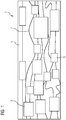
- FIG. 1 shows a schematic representation of a backplane 1 in a plan view of the backplane 1.
- a plurality of electrical components 3 are arranged on the backplane 1.
- An electrical component 3 may be, for example, a contactor, a switch, a control unit, an input / output unit, a soft starter or a frequency converter.
- the backplane 1 has a carrier plate 5, conductor tracks 7 arranged on the carrier plate 5 and sensor units 9 integrated in the carrier plate 5.
- the conductor tracks 7 each connect electrical components 3 and / or sensor units 9 to one another electrically.
- a sensor unit 9 may include, for example, a current sensor for detecting an electric current, a voltage sensor for detecting an electric voltage, a temperature sensor for detecting a temperature, a power sensor for detecting an electric power, a strain sensor for detecting deformation of the carrier plate 5, a vibration sensor for detecting vibration of the carrier plate 5, an acceleration sensor for detecting acceleration of the carrier plate 5, a light sensor, a magnetometer, a gas sensor, a proximity switch or an evaluation unit have to evaluate sensor signals.
- the sensor units 9 are integrated into the carrier plate 5 by an additive manufacturing process.
- the carrier plate 5 is produced at least in each region surrounding a sensor unit 9 with a 3D print which embeds the respective sensor unit 9 in the carrier plate 5.
- the conductor tracks 7 are applied to the carrier plate 5, for example, with a 3D print.
- the printed conductors 7 are printed from an electrically conductive paste, in particular from a copper paste, aluminum paste, brass paste or silver paste, which is hardened after application to the carrier plate 5.
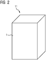
- FIG. 2 shows a perspective view of a cabinet 11.
- the cabinet 11 has a backplane 1 described with reference to FIG 1, which forms a rear wall of the cabinet 11.
Priority Applications (5)
| Application Number | Priority Date | Filing Date | Title |
|---|---|---|---|
| EP18169242.7A EP3562285A1 (fr) | 2018-04-25 | 2018-04-25 | Dispositif de raccordement des composants électriques |
| EP19720451.4A EP3741194A1 (fr) | 2018-04-25 | 2019-04-15 | Connexion de composants électriques |
| PCT/EP2019/059608 WO2019206698A1 (fr) | 2018-04-25 | 2019-04-15 | Connexion de composants électriques |
| US17/047,763 US20210176885A1 (en) | 2018-04-25 | 2019-04-15 | Connecting electrical components |
| CN201980027564.5A CN112020904B (zh) | 2018-04-25 | 2019-04-15 | 电气构件的连接 |
Applications Claiming Priority (1)
| Application Number | Priority Date | Filing Date | Title |
|---|---|---|---|
| EP18169242.7A EP3562285A1 (fr) | 2018-04-25 | 2018-04-25 | Dispositif de raccordement des composants électriques |
Publications (1)
| Publication Number | Publication Date |
|---|---|
| EP3562285A1 true EP3562285A1 (fr) | 2019-10-30 |
Family
ID=62063405
Family Applications (2)
| Application Number | Title | Priority Date | Filing Date |
|---|---|---|---|
| EP18169242.7A Withdrawn EP3562285A1 (fr) | 2018-04-25 | 2018-04-25 | Dispositif de raccordement des composants électriques |
| EP19720451.4A Withdrawn EP3741194A1 (fr) | 2018-04-25 | 2019-04-15 | Connexion de composants électriques |
Family Applications After (1)
| Application Number | Title | Priority Date | Filing Date |
|---|---|---|---|
| EP19720451.4A Withdrawn EP3741194A1 (fr) | 2018-04-25 | 2019-04-15 | Connexion de composants électriques |
Country Status (4)
| Country | Link |
|---|---|
| US (1) | US20210176885A1 (fr) |
| EP (2) | EP3562285A1 (fr) |
| CN (1) | CN112020904B (fr) |
| WO (1) | WO2019206698A1 (fr) |
Cited By (1)
| Publication number | Priority date | Publication date | Assignee | Title |
|---|---|---|---|---|
| EP4154995A1 (fr) * | 2021-09-23 | 2023-03-29 | Siemens Aktiengesellschaft | Unité d'application et de raclage de matière |
Families Citing this family (1)
| Publication number | Priority date | Publication date | Assignee | Title |
|---|---|---|---|---|
| EP4156875A1 (fr) * | 2021-09-23 | 2023-03-29 | Siemens Aktiengesellschaft | Procédé d'établissement d'une connexion électrique et/ou de communication |
Citations (4)
| Publication number | Priority date | Publication date | Assignee | Title |
|---|---|---|---|---|
| DE69114682T2 (de) * | 1991-01-18 | 1996-07-18 | Alain Arnaud | Elektrisches Kontroll- und Steuerungssystem einer Funktionseinheit, insbesondere eines Hauses eines Gebäudes, eines Schiffes oder dergleichen. |
| US7321313B1 (en) * | 2003-07-30 | 2008-01-22 | Tellabs Operations, Inc. | Electronic insertion/extraction cycle counter and logger device |
| US20160236770A1 (en) * | 2015-02-16 | 2016-08-18 | Hamilton Sundstrand Corporation | Electronic Control with Interchangeable Subsystem Modules |
| DE102016002052A1 (de) | 2015-12-18 | 2017-06-22 | Liebherr-Components Biberach Gmbh | Schaltschrank sowie Verfahren zu dessen Herstellung |
Family Cites Families (36)
| Publication number | Priority date | Publication date | Assignee | Title |
|---|---|---|---|---|
| US4406987A (en) * | 1981-03-20 | 1983-09-27 | Fuji Xerox Co., Ltd. | Charge level sensor |
| DE19808248A1 (de) * | 1998-02-27 | 1999-09-02 | Pierburg Ag | Meßvorrichtung zur Messung der Masse eines strömenden Mediums |
| US8099054B2 (en) * | 1999-04-27 | 2012-01-17 | Joseph Akwo Tabe | Mega communication and media apparatus configured for energy harvesting and for boosting signal reception to prevent brain cancerous deseases |
| JP4501097B2 (ja) * | 2001-01-12 | 2010-07-14 | 横浜ゴム株式会社 | タイヤ装着用トランスポンダ及びトランスポンダ装着タイヤの製造方法 |
| DE102004020829B4 (de) * | 2004-04-28 | 2006-05-18 | Fraunhofer-Gesellschaft zur Förderung der angewandten Forschung e.V. | Sensor für die Detektion von Inhaltsstoffen von Flüssigkeiten, insbesondere biologischer Materialien, und diesen Sensor enthaltende Detektionsvorrichtung |
| DE102005025754B4 (de) * | 2005-06-02 | 2019-08-08 | Infineon Technologies Ag | Halbleitersensorbauteil mit einem Sensorchip und Verfahren zur Herstellung von Halbleitersensorbauteilen |
| US8899487B2 (en) * | 2005-08-18 | 2014-12-02 | Ivi Holdings Ltd. | Biometric identity verification system and method |
| US7572665B2 (en) * | 2005-10-21 | 2009-08-11 | Wisconsin Alumni Research Foundation | Microelectronics grade metal substrate, related metal-embedded devices and methods for fabricating same |
| US7537511B2 (en) * | 2006-03-14 | 2009-05-26 | Micron Technology, Inc. | Embedded fiber acoustic sensor for CMP process endpoint |
| US7698962B2 (en) * | 2006-04-28 | 2010-04-20 | Amsted Rail Company, Inc. | Flexible sensor interface for a railcar truck |
| US7638874B2 (en) * | 2006-06-23 | 2009-12-29 | Intel Corporation | Microelectronic package including temperature sensor connected to the package substrate and method of forming same |
| US7911010B2 (en) * | 2006-07-17 | 2011-03-22 | Kwj Engineering, Inc. | Apparatus and method for microfabricated multi-dimensional sensors and sensing systems |
| US7617599B2 (en) * | 2007-12-05 | 2009-11-17 | Memsic, Inc. | Sensor packaging method for a human contact interface |
| DE102008043517B4 (de) * | 2008-11-06 | 2022-03-03 | Robert Bosch Gmbh | Sensormodul und Verfahren zur Herstellung eines Sensormoduls |
| US20110140844A1 (en) * | 2009-12-15 | 2011-06-16 | Mcguire Kenneth Stephen | Packaged product having a reactive label and a method of its use |
| US8889021B2 (en) * | 2010-01-21 | 2014-11-18 | Kla-Tencor Corporation | Process condition sensing device and method for plasma chamber |
| JP5557960B2 (ja) * | 2010-08-06 | 2014-07-23 | ディ・エヌ・エイ・エレクトロニクス・リミテッド | 無線で接続されたチップ上の流体センサ |
| JP5743070B2 (ja) * | 2011-03-23 | 2015-07-01 | セイコーエプソン株式会社 | 液体噴射ヘッド及び液体噴射装置 |
| US8520114B2 (en) * | 2011-06-01 | 2013-08-27 | Global Oled Technology Llc | Apparatus for displaying and sensing images |
| TWI577001B (zh) * | 2011-10-04 | 2017-04-01 | Sony Corp | 固體攝像裝置、固體攝像裝置之製造方法及電子機器 |
| US9302826B2 (en) * | 2013-03-13 | 2016-04-05 | Capton, Inc. | Spout apparatus, systems and methods |
| AT515443B1 (de) * | 2014-02-28 | 2019-10-15 | At & S Austria Tech & Systemtechnik Ag | Verfahren zum Herstellen einer Leiterplatte sowie Leiterplatte |
| US9383550B2 (en) * | 2014-04-04 | 2016-07-05 | Qualcomm Incorporated | Auto-focus in low-profile folded optics multi-camera system |
| CN104552708B (zh) * | 2014-06-24 | 2017-11-07 | 深圳青铜剑科技股份有限公司 | 一种制作导热硅胶片的模具及其使用方法 |
| US20180125365A1 (en) * | 2014-09-17 | 2018-05-10 | Canary Medical Inc. | Devices, systems and methods for using and monitoring medical devices |
| CA2965190A1 (fr) * | 2014-10-23 | 2016-04-28 | Facebook, Inc. | Fabrication de traces conductrices intra-structures et interconnexions pour les structures de fabrication tridimensionnelle |
| CN107405826A (zh) * | 2015-03-17 | 2017-11-28 | 飞利浦照明控股有限公司 | 制作具有互连和嵌入式部件的3d打印形状 |
| CN105241585B (zh) * | 2015-11-12 | 2017-08-18 | 桂林电子科技大学 | 一种基于银导电胶的电容式传感器装置及其制作方法 |
| JP6939568B2 (ja) * | 2016-01-15 | 2021-09-22 | ソニーグループ株式会社 | 半導体装置および撮像装置 |
| US10203398B2 (en) * | 2016-05-04 | 2019-02-12 | Ting-Yi Chen | Optical proximity sensor and manufacturing method thereof |
| DE112016006900B4 (de) * | 2016-05-25 | 2022-01-27 | Intel Corporation | Gehäuse einer integrierten Schaltung, Rechenvorrichtung, Verfahren zum Herstellen eines Substrats für ein Gehäuse einer integrierten Schaltung sowie Verfahren zum Betreiben eines Gehäuses einer integrierten Schaltung |
| US10695564B2 (en) * | 2016-06-02 | 2020-06-30 | Battelle Memorial Institute | Flexible sheet for neuromuscular stimulation |
| US20180061696A1 (en) * | 2016-08-23 | 2018-03-01 | Applied Materials, Inc. | Edge ring or process kit for semiconductor process module |
| JP6819163B2 (ja) * | 2016-09-12 | 2021-01-27 | 株式会社デンソーウェーブ | 絶縁型信号伝達装置、電子機器 |
| CN110383036A (zh) * | 2016-12-18 | 2019-10-25 | 科来徳创新有限公司 | 环境模块化系统装置 |
| US20180226515A1 (en) * | 2017-02-06 | 2018-08-09 | Semiconductor Components Industries, Llc | Semiconductor device and method of forming embedded thermoelectric cooler for heat dissipation of image sensor |
-
2018
- 2018-04-25 EP EP18169242.7A patent/EP3562285A1/fr not_active Withdrawn
-
2019
- 2019-04-15 EP EP19720451.4A patent/EP3741194A1/fr not_active Withdrawn
- 2019-04-15 CN CN201980027564.5A patent/CN112020904B/zh not_active Expired - Fee Related
- 2019-04-15 US US17/047,763 patent/US20210176885A1/en not_active Abandoned
- 2019-04-15 WO PCT/EP2019/059608 patent/WO2019206698A1/fr active Search and Examination
Patent Citations (4)
| Publication number | Priority date | Publication date | Assignee | Title |
|---|---|---|---|---|
| DE69114682T2 (de) * | 1991-01-18 | 1996-07-18 | Alain Arnaud | Elektrisches Kontroll- und Steuerungssystem einer Funktionseinheit, insbesondere eines Hauses eines Gebäudes, eines Schiffes oder dergleichen. |
| US7321313B1 (en) * | 2003-07-30 | 2008-01-22 | Tellabs Operations, Inc. | Electronic insertion/extraction cycle counter and logger device |
| US20160236770A1 (en) * | 2015-02-16 | 2016-08-18 | Hamilton Sundstrand Corporation | Electronic Control with Interchangeable Subsystem Modules |
| DE102016002052A1 (de) | 2015-12-18 | 2017-06-22 | Liebherr-Components Biberach Gmbh | Schaltschrank sowie Verfahren zu dessen Herstellung |
Cited By (2)
| Publication number | Priority date | Publication date | Assignee | Title |
|---|---|---|---|---|
| EP4154995A1 (fr) * | 2021-09-23 | 2023-03-29 | Siemens Aktiengesellschaft | Unité d'application et de raclage de matière |
| WO2023046353A1 (fr) | 2021-09-23 | 2023-03-30 | Siemens Aktiengesellschaft | Unité pour appliquer et racler un matériau |
Also Published As
| Publication number | Publication date |
|---|---|
| CN112020904A (zh) | 2020-12-01 |
| CN112020904B (zh) | 2021-12-10 |
| EP3741194A1 (fr) | 2020-11-25 |
| WO2019206698A1 (fr) | 2019-10-31 |
| US20210176885A1 (en) | 2021-06-10 |
Similar Documents
| Publication | Publication Date | Title |
|---|---|---|
| DE10119458B4 (de) | Schaltgeräteeinheit für einen Verbraucher, insbesondere Motorstarter | |
| EP2745179B1 (fr) | Élément de base pour supporter un module de protection contre les surtensions et système de bus modulaire | |
| DE102008012665A1 (de) | Strommessvorrichtung mittels magnetempfindlichem Sensor für ein leistungselektronisches System | |
| DE202014102609U1 (de) | Hochvolt-Verteilerbox insbesondere für ein Kraftfahrzeug | |
| EP3562285A1 (fr) | Dispositif de raccordement des composants électriques | |
| DE102017005306A1 (de) | Leitungsüberwachung auf Beschädigung der Ummantelung | |
| DE102017212493A1 (de) | Elektrischer Steckverbinder, Anordnung mit einem elektrischen Steckverbinder, Verwendung eines elektrischen Steckverbinders und Verfahren zum Betrieb eines elektrischen Steckverbinders | |
| DE102004057330B3 (de) | Vorrichtung zur Überwachung eines Leitungsnetzes, insbesondere eines Kraftfahrzeug-Bordnetzes sowie Verfahren zum Überwachen eines solchen Leitungsnetzes | |
| EP1755135A2 (fr) | Circuit électrique pour la collection et l'évaluation des variables mesurées électriques et physiques dans un interrupteur électrique | |
| EP3738415B1 (fr) | Fond de panier et son procédé de fabrication | |
| DE69819983T2 (de) | Stromverteilungssystem | |
| DE102012023460A1 (de) | Kraftfahrzeug-Bordnetz und Verfahren zum Erkennen eines Lichtbogens in einem Kraftfahrzeug-Bordnetz | |
| DE102021203038B4 (de) | Temperaturüberwachung für Schaltanlagen | |
| EP3562283A1 (fr) | Arrangement modulaire backplane | |
| DE102012201514A1 (de) | Schütz | |
| DE102019215133A1 (de) | Schutz- oder Steuergerät für ein Mittel- oder Hochspannungsversorgungsnetz sowie Erdungsstecker für ein solches Gerät | |
| EP3899558A1 (fr) | Procédé et dispositif de contrôle | |
| EP3340200A1 (fr) | Système de détection d'incendie pour un véhicule ferroviaire | |
| DE102021213290A1 (de) | Verfahren zum Betreiben einer Schaltanlage und Schaltanlage | |
| DE102017005589A1 (de) | Interlocksystem zum Überwachen zumindest einer Hochvolt-Komponente eines Kraftfahrzeugs, Hochvolt-Komponente, Hochvolt-System sowie Verfahren | |
| DE102020000854A1 (de) | Steuervorrichtungs-montagesystem und steuervorrichtungseinheit | |
| DE102008043627B4 (de) | Vorrichtung zur elektrischen Ansteuerung einer Sitzgruppe und ein Verfahren zum elektrischen Ansteuern einer Sitzgruppe | |
| DE102010045973B4 (de) | Vorrichtung zur Überwachung von Strömen | |
| EP3562284B1 (fr) | Procédé de fabrication d'un fond de panier et armoire de commande comprenant un tel de fon de panier | |
| DE102008045337B4 (de) | Verteileranschlussmodul |
Legal Events
| Date | Code | Title | Description |
|---|---|---|---|
| PUAI | Public reference made under article 153(3) epc to a published international application that has entered the european phase |
Free format text: ORIGINAL CODE: 0009012 |
|
| AK | Designated contracting states |
Kind code of ref document: A1 Designated state(s): AL AT BE BG CH CY CZ DE DK EE ES FI FR GB GR HR HU IE IS IT LI LT LU LV MC MK MT NL NO PL PT RO RS SE SI SK SM TR |
|
| AX | Request for extension of the european patent |
Extension state: BA ME |
|
| STAA | Information on the status of an ep patent application or granted ep patent |
Free format text: STATUS: THE APPLICATION IS DEEMED TO BE WITHDRAWN |
|
| 18D | Application deemed to be withdrawn |
Effective date: 20200603 |