EP3561878A1 - Method to remove iii-v materials in high aspect ratio structures - Google Patents
Method to remove iii-v materials in high aspect ratio structures Download PDFInfo
- Publication number
- EP3561878A1 EP3561878A1 EP19168988.4A EP19168988A EP3561878A1 EP 3561878 A1 EP3561878 A1 EP 3561878A1 EP 19168988 A EP19168988 A EP 19168988A EP 3561878 A1 EP3561878 A1 EP 3561878A1
- Authority
- EP
- European Patent Office
- Prior art keywords
- fin
- substrate
- features
- etching
- remaining portion
- Prior art date
- Legal status (The legal status is an assumption and is not a legal conclusion. Google has not performed a legal analysis and makes no representation as to the accuracy of the status listed.)
- Withdrawn
Links
Images




Classifications
-
- H—ELECTRICITY
- H10—SEMICONDUCTOR DEVICES; ELECTRIC SOLID-STATE DEVICES NOT OTHERWISE PROVIDED FOR
- H10D—INORGANIC ELECTRIC SEMICONDUCTOR DEVICES
- H10D30/00—Field-effect transistors [FET]
- H10D30/01—Manufacture or treatment
- H10D30/021—Manufacture or treatment of FETs having insulated gates [IGFET]
- H10D30/024—Manufacture or treatment of FETs having insulated gates [IGFET] of fin field-effect transistors [FinFET]
-
- H—ELECTRICITY
- H10—SEMICONDUCTOR DEVICES; ELECTRIC SOLID-STATE DEVICES NOT OTHERWISE PROVIDED FOR
- H10P—GENERIC PROCESSES OR APPARATUS FOR THE MANUFACTURE OR TREATMENT OF DEVICES COVERED BY CLASS H10
- H10P50/00—Etching of wafers, substrates or parts of devices
- H10P50/20—Dry etching; Plasma etching; Reactive-ion etching
- H10P50/24—Dry etching; Plasma etching; Reactive-ion etching of semiconductor materials
- H10P50/242—Dry etching; Plasma etching; Reactive-ion etching of semiconductor materials of Group IV materials
-
- H—ELECTRICITY
- H10—SEMICONDUCTOR DEVICES; ELECTRIC SOLID-STATE DEVICES NOT OTHERWISE PROVIDED FOR
- H10D—INORGANIC ELECTRIC SEMICONDUCTOR DEVICES
- H10D30/00—Field-effect transistors [FET]
- H10D30/01—Manufacture or treatment
- H10D30/021—Manufacture or treatment of FETs having insulated gates [IGFET]
-
- H—ELECTRICITY
- H10—SEMICONDUCTOR DEVICES; ELECTRIC SOLID-STATE DEVICES NOT OTHERWISE PROVIDED FOR
- H10D—INORGANIC ELECTRIC SEMICONDUCTOR DEVICES
- H10D30/00—Field-effect transistors [FET]
- H10D30/60—Insulated-gate field-effect transistors [IGFET]
- H10D30/62—Fin field-effect transistors [FinFET]
- H10D30/6211—Fin field-effect transistors [FinFET] having fin-shaped semiconductor bodies integral with the bulk semiconductor substrates
-
- H—ELECTRICITY
- H10—SEMICONDUCTOR DEVICES; ELECTRIC SOLID-STATE DEVICES NOT OTHERWISE PROVIDED FOR
- H10D—INORGANIC ELECTRIC SEMICONDUCTOR DEVICES
- H10D30/00—Field-effect transistors [FET]
- H10D30/60—Insulated-gate field-effect transistors [IGFET]
- H10D30/62—Fin field-effect transistors [FinFET]
- H10D30/6215—Fin field-effect transistors [FinFET] having multiple independently-addressable gate electrodes
-
- H—ELECTRICITY
- H10—SEMICONDUCTOR DEVICES; ELECTRIC SOLID-STATE DEVICES NOT OTHERWISE PROVIDED FOR
- H10D—INORGANIC ELECTRIC SEMICONDUCTOR DEVICES
- H10D30/00—Field-effect transistors [FET]
- H10D30/60—Insulated-gate field-effect transistors [IGFET]
- H10D30/62—Fin field-effect transistors [FinFET]
- H10D30/6219—Fin field-effect transistors [FinFET] characterised by the source or drain electrodes
-
- H—ELECTRICITY
- H10—SEMICONDUCTOR DEVICES; ELECTRIC SOLID-STATE DEVICES NOT OTHERWISE PROVIDED FOR
- H10D—INORGANIC ELECTRIC SEMICONDUCTOR DEVICES
- H10D30/00—Field-effect transistors [FET]
- H10D30/60—Insulated-gate field-effect transistors [IGFET]
- H10D30/751—Insulated-gate field-effect transistors [IGFET] having composition variations in the channel regions
-
- H—ELECTRICITY
- H10—SEMICONDUCTOR DEVICES; ELECTRIC SOLID-STATE DEVICES NOT OTHERWISE PROVIDED FOR
- H10D—INORGANIC ELECTRIC SEMICONDUCTOR DEVICES
- H10D84/00—Integrated devices formed in or on semiconductor substrates that comprise only semiconducting layers, e.g. on Si wafers or on GaAs-on-Si wafers
- H10D84/01—Manufacture or treatment
- H10D84/0123—Integrating together multiple components covered by H10D12/00 or H10D30/00, e.g. integrating multiple IGBTs
- H10D84/0126—Integrating together multiple components covered by H10D12/00 or H10D30/00, e.g. integrating multiple IGBTs the components including insulated gates, e.g. IGFETs
- H10D84/0158—Integrating together multiple components covered by H10D12/00 or H10D30/00, e.g. integrating multiple IGBTs the components including insulated gates, e.g. IGFETs the components including FinFETs
-
- H—ELECTRICITY
- H10—SEMICONDUCTOR DEVICES; ELECTRIC SOLID-STATE DEVICES NOT OTHERWISE PROVIDED FOR
- H10D—INORGANIC ELECTRIC SEMICONDUCTOR DEVICES
- H10D84/00—Integrated devices formed in or on semiconductor substrates that comprise only semiconducting layers, e.g. on Si wafers or on GaAs-on-Si wafers
- H10D84/01—Manufacture or treatment
- H10D84/02—Manufacture or treatment characterised by using material-based technologies
- H10D84/05—Manufacture or treatment characterised by using material-based technologies using Group III-V technology
-
- H—ELECTRICITY
- H10—SEMICONDUCTOR DEVICES; ELECTRIC SOLID-STATE DEVICES NOT OTHERWISE PROVIDED FOR
- H10P—GENERIC PROCESSES OR APPARATUS FOR THE MANUFACTURE OR TREATMENT OF DEVICES COVERED BY CLASS H10
- H10P50/00—Etching of wafers, substrates or parts of devices
- H10P50/20—Dry etching; Plasma etching; Reactive-ion etching
- H10P50/28—Dry etching; Plasma etching; Reactive-ion etching of insulating materials
- H10P50/282—Dry etching; Plasma etching; Reactive-ion etching of insulating materials of inorganic materials
- H10P50/283—Dry etching; Plasma etching; Reactive-ion etching of insulating materials of inorganic materials by chemical means
Definitions
- Embodiments of the present invention generally relate to methods for forming semiconductor devices, and more particularly to methods for forming fin field effect transistors (FinFets).
- FinFets fin field effect transistors
- FinFET devices typically include semiconductor fins with high aspect ratios in which the channel and source/drain regions for the transistor are formed thereover. A gate electrode is then formed over and alongside of a portion of the fin devices utilizing the advantage of the increased surface area of the channel and source/drain regions to produce faster, more reliable and better-controlled semiconductor transistor devices. Further advantages of FinFETs include reducing the short channel effect and providing higher current flow.
- III-V materials such as GaAs, InGaAs, and InP on patterned wafers.
- Such challenges include selectively etching the III-V semiconductor materials versus Si, SiO x , and SiN x ; difficulty in reaching the bottom of the trenches ( ⁇ 30 nm) in high aspect ratio structures; thermal budget limitations; and arsenic contamination and abatement constraints for the substrate processing chamber.
- a fin structure processing method includes removing a portion of a first fin of a plurality of fins formed on a substrate to expose a surface of a remaining portion of the first fin, wherein the fins are adjacent to dielectric material structures formed on the substrate; performing a deposition operation to form features on the surface of the remaining portion of the first fin by depositing a Group III-V semiconductor material in a substrate processing environment; and performing an etching operation to etch the features with an etching gas to form a plurality of openings between adjacent dielectric material structures, wherein the etching operation is performed in the same chamber as the deposition operation.
- a fin structure processing method includes removing a portion of a first fin of a plurality of fins formed on a substrate to expose a surface of a remaining portion of the first fin, wherein the fins are adjacent to dielectric material structures formed on the substrate; performing a deposition operation to form features on the surface of the remaining portion of the first fin by depositing a Group III-V semiconductor material in a substrate processing environment; planarizing the Group III-V semiconductor material by a chemical mechanical polishing process; performing an etching operation to etch the features with an etching gas to form a plurality of openings between adjacent dielectric material structures, wherein the etching operation is performed in the same chamber as the deposition operation; and forming a fill material on the surface of the remaining portion of the first fin, wherein the fill material is formed within a corresponding opening of the plurality of openings.
- a fin structure processing method includes removing a portion of a first fin of a plurality of fins formed on a substrate to expose a surface of a remaining portion of the first fin, wherein the fins are adjacent to dielectric material structures formed on the substrate; performing a deposition operation to form features on the surface of the remaining portion of the first fin by depositing a Group III-V semiconductor material in a substrate processing environment; planarizing the Group III-V semiconductor material by a chemical mechanical polishing process; performing an etching operation to etch the features with an etching gas to form a plurality of openings between adjacent dielectric material structures, wherein the etching operation is performed in the same chamber as the deposition operation and wherein the etching gas is HCI; delivering a hydrogen containing gas, a carrier gas, or a combination thereof, to the substrate processing environment; and forming a fill material on the surface of the remaining portion of the first fin, wherein the fill material is formed within a corresponding opening of the plurality of openings.
- FIG. 1 is a perspective view of a semiconductor structure 100 according to one embodiment described herein.
- the semiconductor structure 100 may include a substrate 101, a plurality of fins 102 (only two are shown, but the structure may have more than two fins), a dielectric material 104 disposed between adjacent fins 102 on the substrate 101, and a gate electrode 110 disposed on the dielectric material 104 and over a portion of each fin 102.
- the substrate 101 may be a bulk silicon substrate, and may be doped with a p-type or an n-type impurity.
- the substrate 101 may, alternatively, be fabricated from other substrate materials that include germanium, silicon-germanium, and other similar materials.
- the plurality of fins 102 may be fabricated from the same material as the substrate 101.
- the dielectric material 104 may form isolation regions, such as shallow trench isolation (STI) regions, and may be fabricated from silicon oxide, silicon nitride, silicon oxynitride, silicon carbonitride, or any other suitable dielectric material. As shown in Figure 1 , each of the plurality of fins 102 extends a distance above the upper surface of the dielectric material 104. A gate dielectric 108 is formed between the gate electrode 110 and the plurality of fins 102. The gate dielectric 108 facilitates electrical isolation between the gate electrode 110 and the plurality of fins 102.
- STI shallow trench isolation
- the gate dielectric 108 may be fabricated from silicon nitride, silicon oxide, hafnium oxide, hafnium silicon oxynitride, hafnium silicate, hafnium silicon oxide, or any other suitable gate dielectric material.
- the gate electrode 110 may be fabricated from polysilicon, amorphous silicon, germanium, silicon germanium, metals, or metal alloys.
- Figures 2A - 2H illustrate a process for forming a semiconductor device according to one embodiment described herein.
- Figure 2A is a side view of the semiconductor structure 100.
- the semiconductor structure 100 includes the plurality of fins 102 (three are shown) extending over an upper surface 201 of the dielectric material 104 and the gate electrode 110.
- the gate dielectric 108 and the substrate 101 are omitted for clarity.
- a portion of each fin 102 is removed to expose a surface 202 of a remaining portion 204 of the fin 102.
- the removal of the portion of each fin 102 may be by a selective etching process, as discussed below, so the gate electrode 110 and the dielectric material 104 are not significantly affected by the removal of the portion of the fins 102.
- the etch chemistry is chosen such that the etch rate of the fin 102 is much faster than the etch rates of the gate electrode 110 and the dielectric material 104 since the fin 102, the gate electrode 110, and the dielectric material 104 are made of different materials.
- the surface 202 of the remaining portion 204 of each fin 102 is recessed from the upper surface 201 of the dielectric material.
- a feature 206 such as a pillar or a ridge, is formed on the surface 202 of the remaining portion 204 of each fin 102.
- the features 206 appear in the foreground, while the gate electrode 110 appears in the background.
- any native oxides formed on the surfaces 201 and 202 may be removed by a pre-clean process.
- the features 206 may be formed in an epitaxial deposition chamber, such as a III-V growth chamber.
- One suitable apparatus for performing epitaxial deposition is the CENTURATM RP Epi platform available from Applied Materials, Inc., Santa Clara, CA.
- each feature 206 is formed in by first forming a nucleation layer on the surface 202 of the remaining portion 204 of each fin 102.
- the substrate 101 ( Figure 1 ) is held at a temperature ranging from about 300 degrees Celsius to about 400 degrees Celsius and the epitaxial deposition chamber may have a pressure less than about 100 Torr during the formation of the nucleation layer.
- the nucleation layer may have a thickness ranging from about 50 Angstroms to about 100 Angstroms.
- the substrate 101 ( Figure 1 ) is heated to a temperature ranging from about 500 degrees Celsius to about 600 degrees Celsius, the pressure of the epitaxial deposition chamber is reduced to from about 10 Torr to about 40 Torr, and the features 206 are formed.
- the materials used to form the nucleation layers and the features 206 include Group III-V semiconductor materials such as aluminum antimonide, aluminum arsenide, aluminum gallium arsenide, aluminum gallium indium phosphide, aluminum gallium nitride, aluminum gallium phosphide, aluminum indium arsenide, aluminum nitride, aluminum phosphide, boron arsenide, boron nitride, boron phosphide, gallium antimonide, gallium arsenide, gallium arsenide phosphide, gallium phosphide, gallium arsenide antimonide, indium antimonide, indium arsenide, indium arsenide antimonide, indium gallium arsenide, indium gallium nitride, indium gallium phosphide, indium nitride, and indium phosphide, among others, and combinations thereof.
- the features and nucleation layers may be formed by epit
- each feature 206 may have a rectangular cross-section and a substantially constant width W 1 over the surface 201 of the remaining portion 204 of each fin 102.
- the width W 1 may be greater than a width W 2 of the remaining portion 204 of the fin 102. In one embodiment, the width W 1 is about 1 nm to about 10 nm wider than the width W 2 .
- a dielectric material 208 is formed between adjacent features 206.
- the dielectric material 208 and the features 206 are coplanar at the end of the deposition process of the dielectric material 208.
- the dielectric material 208 is also formed on the features 206 and the gate electrode 110.
- the dielectric material 208 may be the same material as the dielectric material 104.
- the dielectric material 208 is silicon oxide and is deposited by a flowable chemical vapor deposition (FCVD) process.
- FCVD flowable chemical vapor deposition
- a chemical mechanical planarization (CMP) process is then performed on the dielectric material 208 to expose the features 206, as shown in Figure 2E .
- a surface 210 of each feature 206 is exposed, and the surfaces 210 are coplanar with a surface 212 of the dielectric material 208.
- the features 206 are removed to expose the surfaces 202 of the remaining portions 204.
- the gate dielectric 108 and the gate electrode 110 should appear in the background but are omitted for clarity.
- the features 206 may be removed by a selective etching process so the dielectric material 208 is not substantially affected. In other words, the etch rate of the feature 206 is much faster than the etch rate of the dielectric material 208 since the feature 206 and the dielectric material 208 are made of different materials.
- the process for etching is described below.
- a plurality of openings 214 such as trenches or vias, is formed in the dielectric material 208. Each opening 214 has the same shape as the feature 206.
- a fill material 216 such as a stressor material, is then deposited in each opening 214 on the surface 202 of the remaining portion 204 of each fin 102, as shown in Figure 2G .
- the fill material 216 may be also deposited on the surface 212 of the dielectric material 208, and an etch back process may be performed to remove the fill material 216 deposited on the surface 212 of the dielectric material 208.
- the fill material 216 may be the source or drain of a FinFET device and may be a silicon and/or germanium based material.
- the fill material 216 is an electrically conductive material.
- the fill material 216 may be formed by an epitaxial deposition process in an epitaxial deposition chamber available from Applied Materials, Inc.
- the epitaxial deposition process is generally performed by flowing epitaxy precursors such as silane, germane, phosphine, and arsine into the epitaxial deposition chamber and heating the substrate to a temperature, for example 300 degrees Celsius to 600 degrees Celsius, that results in epitaxial deposition on the substrate.
- precursors for the Group III elements include halides, which can be reacted with materials such as arsine, phosphine, and stilbene.
- the fill material 216 is silicon doped with phosphorus and the FinFET device is an n-type FET.
- the fill material 216 is silicon germanium doped with boron or gallium, and the FinFET device is a p-type FET.
- the shape of the fill material 216 is constrained by the opening 214 that the fill material 216 is formed therein.
- the fill material 216 instead of having a diamond shape, the fill material 216 has a rectangular cross-section, and the distance between adjacent fill materials 216 is increased.
- Each fill material 216 has a surface 213 that is recessed from the surface 212 of the dielectric material 208.
- any material deposited on the surface 213 of the fill material 216 within the opening 214 is self-aligned.
- a metal contact 222 is deposited over the fill material 216 within the opening 214, as shown in Figure 2H .
- the metal contact 222 is self-aligned to the fill material 216, i.e. , a source or drain, since both the metal contact 222 and the fill material 216 are formed within the opening 214.
- the metal contact 222 may be fabricated from a metal such as cobalt or tungsten. Additional materials may be formed on the fill material 216 prior to the deposition of the metal contact 222.
- a silicide or germanide layer 218 may be formed on the fill material 216 by a silicidation process.
- a liner 220 may be formed conformally in the opening 214 by an atomic layer deposition (ALD) process.
- the metal contact 222 is then deposited on the liner 220.
- a CMP process may be performed to planarize the surface.
- one suitable apparatus for performing the etching process is the CENTURATM RP Epi platform available from Applied Materials, Inc., Santa Clara, CA. It is contemplated that other suitably configured apparatus from other manufacturers may also be utilized in accordance with the embodiments described herein.
- selective etching is utilized to remove the III-V structures. For example, etch chemistries selective to III-V materials are utilized to remove the features 206 preferentially to the oxide and/or nitride containing gap fill material. The etching operation may be performed in the same chamber as the deposition operation.
- a chlorine containing gas such as HCI
- the chlorine containing gas is optionally delivered to a substrate processing environment with a hydrogen containing gas, such as H 2 .
- the chlorine containing gas is optionally delivered to a substrate processing environment with a relatively nonreactive carrier gas such as N 2 or Ar.
- the HCI is delivered to the substrate processing environment at a flow rate of between about 1 sccm and about 500 sccm, for a 300 mm wafer.
- the nonreactive carrier gas is delivered to the substrate processing environment at a flow rate of between about 1 slm and about 20 slm.
- a temperature of the wafer is maintained between about 300°C and about 800°C and a pressure of the substrate processing environment is maintained between about 0 Torr and about 100 Torr.
- HCl is used instead of a mixture of HCl and H 2 O because H 2 O oxidizes the surface of the silicon surfaces.
- Using an HCl etch gas with a mass flow of 1-500 sccm at low temperatures (less than about 800°C) reduces the damage to the Si, SiO x and SiN x materials.
- using low pressure etch processes (less than about 100 Torr) allows the gas to reach the bottom of the deep trenches of the high aspect ratio features.
- Figures 3A - 3C illustrate a process for forming a semiconductor device according to another embodiment described herein.
- Figure 3A is a side view of the semiconductor structure 300.
- the semiconductor structure 300 includes a substrate 302 having a semiconductor surface 305.
- the semiconductor surface 305 includes a plurality of exposed portions 304 separated by a plurality of covered portions 306.
- the substrate 302 is a silicon substrate, and the semiconductor surface 305 is a silicon surface.
- a first dielectric material 308 is disposed on the covered portions 306 of the semiconductor surface 305.
- the first dielectric material 308 may be silicon oxide, silicon nitride, silicon oxynitride, silicon carbonitride, or any other suitable dielectric material.
- a feature 310 is formed on each exposed portion 304 of the semiconductor surface 305.
- the features 310 may be the same as the features 206.
- any native oxides formed on the semiconductor surface 305 may be removed by a pre-clean process.
- the features 310 may be formed in an epitaxial deposition chamber.
- each feature 310 is formed in by first forming a nucleation layer on a corresponding exposed portion 304 of the semiconductor surface 305.
- the nucleation layer and the features 310 may be formed under the same process conditions as the nucleation layer and the features 206.
- the materials used to form the features 310 do not form a diamond shape.
- the height, width and facets of the features 310 can be controlled by temperature, pressure and/or precursor flow.
- a second dielectric material 312 is formed between adjacent features 310.
- the second dielectric material 312 and the features 310 are coplanar at the end of the deposition process of the second dielectric material 312.
- the second dielectric material 312 is also formed on the features 310 and a CMP process is performed on the second dielectric material 312 to expose the features 310.
- the second dielectric material 312 may be the same material as the dielectric material 208.
- Process operations shown in Figures 2F , 2G and 2H are then performed on the semiconductor structure 300 to form a plurality of openings in the second dielectric material 312, to deposit a fill material in the plurality of openings, and to deposit a metal in the plurality of openings.
- the fill material may be the same as the fill material 216, and the metal may be the same as the metal contact 222.
- the fill material and the metal are self-aligned since both materials are formed within the same opening.
- FIG. 4A illustrates operations of a method 400 for fin structure processing according to some embodiments.
- the method 400 includes removing a portion of a first fin of a plurality of fins formed on a semiconductor substrate to expose a surface of a remaining portion of the first fin, wherein the fins are adjacent to dielectric material structures formed on the semiconductor substrate at operation 402.
- Method 400 further includes forming features on the surface of the remaining portion of the first fin by depositing a Group III-V semiconductor material in a substrate processing environment at operation 404.
- the method 400 further includes etching the features with an etching gas to form a plurality of openings between adjacent dielectric material structures at operation 408.
- the etching gas is a chlorine containing gas.
- the etching gas is delivered to the substrate processing environment with a hydrogen containing gas and/or a carrier gas, as described above.
- FIG. 4B illustrates operations of a method 420 for fin structure processing according to some embodiments.
- the method 420 includes removing a portion of a first fin of a plurality of fins formed on a semiconductor substrate to expose a surface of a remaining portion of the first fin, wherein the fins are adjacent to dielectric material structures formed on the semiconductor substrate at operation 402.
- Method 420 further includes forming features on the surface of the remaining portion of the first fin by depositing a Group III-V semiconductor material in a substrate processing environment at operation 404.
- the method 420 further includes planarizing the Group III-V semiconductor material by a chemical mechanical polishing process (CMP) at operation 406.
- CMP chemical mechanical polishing process
- the method 420 further includes etching the features with an etching gas to form a plurality of openings between adjacent dielectric material structures at operation 408.
- the etching gas is a chlorine containing gas.
- the etching gas is delivered to the substrate processing environment with a hydrogen containing gas and/or a carrier gas.
- the method 420 further includes forming a fill material on the surface of the remaining portion of the first fin, wherein the fill material is formed within a corresponding opening of the plurality of openings at operation 412.
- FIG. 4C illustrates operations of a method 430 for fin structure processing according to some embodiments.
- the method 430 includes removing a portion of a first fin of a plurality of fins formed on a semiconductor substrate to expose a surface of a remaining portion of the first fin, wherein the fins are adjacent to dielectric material structures formed on the semiconductor substrate at operation 402.
- Method 430 further includes forming features on the surface of the remaining portion of the first fin by depositing a Group III-V semiconductor material in a substrate processing environment at operation 404.
- the method 430 further includes planarizing the Group III-V semiconductor material by a chemical mechanical polishing process at operation 406.
- the method 430 further includes etching the features with an etching gas to form a plurality of openings between adjacent dielectric material structures at operation 408.
- the etching gas is a chlorine containing gas.
- the method 430 delivering a hydrogen containing gas, a carrier gas, or a combination thereof to the substrate processing environment at operation 410.
- the method 430 further includes forming a fill material on the surface of the remaining portion of the first fin, wherein the fill material is formed within a corresponding opening of the plurality of openings at operation 412.
- the III-V growth chamber is connected to a chamber abatement apparatus.
- the chamber abatement apparatus includes an absorber that can be used for abatement of a species, such as an arsenic containing material.
- the chamber abatement apparatus allows removing arsenic, for example, from the effluent stream flowing from the substrate processing chamber.
- Conventional etch tools do not have a dedicated abatement apparatus. Therefore, unlike conventional etch tools, the use of the III-V growth chamber for etch avoids contamination and abatement issues because the III-V growth chamber is equipped with a chamber abatement apparatus that is connected to the effluent flowing from the substrate processing chamber.
- the method 400 includes removing a species (such as an arsenic containing material) from an effluent stream flowing from the substrate processing chamber by a chamber abatement apparatus at operation 414.
- a species such as an arsenic containing material
- the chamber abatement apparatus includes an absorber.
Landscapes
- Insulated Gate Type Field-Effect Transistor (AREA)
- Drying Of Semiconductors (AREA)
Abstract
Description
- Embodiments of the present invention generally relate to methods for forming semiconductor devices, and more particularly to methods for forming fin field effect transistors (FinFets).
- FinFET devices typically include semiconductor fins with high aspect ratios in which the channel and source/drain regions for the transistor are formed thereover. A gate electrode is then formed over and alongside of a portion of the fin devices utilizing the advantage of the increased surface area of the channel and source/drain regions to produce faster, more reliable and better-controlled semiconductor transistor devices. Further advantages of FinFETs include reducing the short channel effect and providing higher current flow.
- Conventional techniques for fabricating FinFETs suffer from challenges during removing or trimming of III-V materials such as GaAs, InGaAs, and InP on patterned wafers. Such challenges include selectively etching the III-V semiconductor materials versus Si, SiOx, and SiNx; difficulty in reaching the bottom of the trenches (< 30 nm) in high aspect ratio structures; thermal budget limitations; and arsenic contamination and abatement constraints for the substrate processing chamber.
- Thus, there is a need for improved methods for fin structure fabrication.
- Methods for forming semiconductor devices, such as FinFETs, are provided. In an embodiment, a fin structure processing method includes removing a portion of a first fin of a plurality of fins formed on a substrate to expose a surface of a remaining portion of the first fin, wherein the fins are adjacent to dielectric material structures formed on the substrate; performing a deposition operation to form features on the surface of the remaining portion of the first fin by depositing a Group III-V semiconductor material in a substrate processing environment; and performing an etching operation to etch the features with an etching gas to form a plurality of openings between adjacent dielectric material structures, wherein the etching operation is performed in the same chamber as the deposition operation.
- In another embodiment, a fin structure processing method includes removing a portion of a first fin of a plurality of fins formed on a substrate to expose a surface of a remaining portion of the first fin, wherein the fins are adjacent to dielectric material structures formed on the substrate; performing a deposition operation to form features on the surface of the remaining portion of the first fin by depositing a Group III-V semiconductor material in a substrate processing environment; planarizing the Group III-V semiconductor material by a chemical mechanical polishing process; performing an etching operation to etch the features with an etching gas to form a plurality of openings between adjacent dielectric material structures, wherein the etching operation is performed in the same chamber as the deposition operation; and forming a fill material on the surface of the remaining portion of the first fin, wherein the fill material is formed within a corresponding opening of the plurality of openings.
- In another embodiment, a fin structure processing method includes removing a portion of a first fin of a plurality of fins formed on a substrate to expose a surface of a remaining portion of the first fin, wherein the fins are adjacent to dielectric material structures formed on the substrate; performing a deposition operation to form features on the surface of the remaining portion of the first fin by depositing a Group III-V semiconductor material in a substrate processing environment; planarizing the Group III-V semiconductor material by a chemical mechanical polishing process; performing an etching operation to etch the features with an etching gas to form a plurality of openings between adjacent dielectric material structures, wherein the etching operation is performed in the same chamber as the deposition operation and wherein the etching gas is HCI; delivering a hydrogen containing gas, a carrier gas, or a combination thereof, to the substrate processing environment; and forming a fill material on the surface of the remaining portion of the first fin, wherein the fill material is formed within a corresponding opening of the plurality of openings.
- So that the manner in which the above recited features of the present disclosure can be understood in detail, a more particular description of the disclosure, briefly summarized above, may be had by reference to embodiments, some of which are illustrated in the appended drawings. It is to be noted, however, that the appended drawings illustrate only exemplary embodiments and are therefore not to be considered limiting of its scope, and may admit to other equally effective embodiments.
-
Figure 1 is a perspective view of a semiconductor structure according to one embodiment described herein. -
Figures 2A - 2H illustrate a process for forming a semiconductor device according to one embodiment described herein. -
Figures 3A - 3C illustrate a process for forming a semiconductor device according to another embodiment described herein. -
Figure 4A illustrates operations of a method for fin structure processing according to some embodiments. -
Figure 4B illustrates operations of a method for fin structure processing according to some embodiments. -
Figure 4C illustrates operations of a method for fin structure processing according to some embodiments. - To facilitate understanding, identical reference numerals have been used, where possible, to designate identical elements that are common to the figures. It is contemplated that elements and features of one embodiment may be beneficially incorporated in other embodiments without further recitation.
-
Figure 1 is a perspective view of asemiconductor structure 100 according to one embodiment described herein. Thesemiconductor structure 100 may include asubstrate 101, a plurality of fins 102 (only two are shown, but the structure may have more than two fins), adielectric material 104 disposed betweenadjacent fins 102 on thesubstrate 101, and agate electrode 110 disposed on thedielectric material 104 and over a portion of eachfin 102. Thesubstrate 101 may be a bulk silicon substrate, and may be doped with a p-type or an n-type impurity. Thesubstrate 101 may, alternatively, be fabricated from other substrate materials that include germanium, silicon-germanium, and other similar materials. The plurality offins 102 may be fabricated from the same material as thesubstrate 101. Thedielectric material 104 may form isolation regions, such as shallow trench isolation (STI) regions, and may be fabricated from silicon oxide, silicon nitride, silicon oxynitride, silicon carbonitride, or any other suitable dielectric material. As shown inFigure 1 , each of the plurality offins 102 extends a distance above the upper surface of thedielectric material 104. A gate dielectric 108 is formed between thegate electrode 110 and the plurality offins 102. The gate dielectric 108 facilitates electrical isolation between thegate electrode 110 and the plurality offins 102. The gate dielectric 108 may be fabricated from silicon nitride, silicon oxide, hafnium oxide, hafnium silicon oxynitride, hafnium silicate, hafnium silicon oxide, or any other suitable gate dielectric material. Thegate electrode 110 may be fabricated from polysilicon, amorphous silicon, germanium, silicon germanium, metals, or metal alloys. -
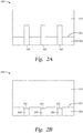
Figures 2A - 2H illustrate a process for forming a semiconductor device according to one embodiment described herein.Figure 2A is a side view of thesemiconductor structure 100. Thesemiconductor structure 100 includes the plurality of fins 102 (three are shown) extending over anupper surface 201 of thedielectric material 104 and thegate electrode 110. The gate dielectric 108 and thesubstrate 101 are omitted for clarity. Next, as shown inFigure 2B , a portion of eachfin 102 is removed to expose asurface 202 of aremaining portion 204 of thefin 102. The removal of the portion of eachfin 102 may be by a selective etching process, as discussed below, so thegate electrode 110 and thedielectric material 104 are not significantly affected by the removal of the portion of thefins 102. In other words, the etch chemistry is chosen such that the etch rate of thefin 102 is much faster than the etch rates of thegate electrode 110 and thedielectric material 104 since thefin 102, thegate electrode 110, and thedielectric material 104 are made of different materials. Thesurface 202 of theremaining portion 204 of eachfin 102 is recessed from theupper surface 201 of the dielectric material. - As shown in
Figure 2C , afeature 206, such as a pillar or a ridge, is formed on thesurface 202 of theremaining portion 204 of eachfin 102. In the view ofFigure 2C , thefeatures 206 appear in the foreground, while thegate electrode 110 appears in the background. Prior to forming thefeatures 206, any native oxides formed on thesurfaces features 206 may be formed in an epitaxial deposition chamber, such as a III-V growth chamber. One suitable apparatus for performing epitaxial deposition is the CENTURA™ RP Epi platform available from Applied Materials, Inc., Santa Clara, CA. In one embodiment, eachfeature 206 is formed in by first forming a nucleation layer on thesurface 202 of theremaining portion 204 of eachfin 102. The substrate 101 (Figure 1 ) is held at a temperature ranging from about 300 degrees Celsius to about 400 degrees Celsius and the epitaxial deposition chamber may have a pressure less than about 100 Torr during the formation of the nucleation layer. The nucleation layer may have a thickness ranging from about 50 Angstroms to about 100 Angstroms. After the formation of the nucleation layers, the substrate 101 (Figure 1 ) is heated to a temperature ranging from about 500 degrees Celsius to about 600 degrees Celsius, the pressure of the epitaxial deposition chamber is reduced to from about 10 Torr to about 40 Torr, and thefeatures 206 are formed. The materials used to form the nucleation layers and thefeatures 206 include Group III-V semiconductor materials such as aluminum antimonide, aluminum arsenide, aluminum gallium arsenide, aluminum gallium indium phosphide, aluminum gallium nitride, aluminum gallium phosphide, aluminum indium arsenide, aluminum nitride, aluminum phosphide, boron arsenide, boron nitride, boron phosphide, gallium antimonide, gallium arsenide, gallium arsenide phosphide, gallium phosphide, gallium arsenide antimonide, indium antimonide, indium arsenide, indium arsenide antimonide, indium gallium arsenide, indium gallium nitride, indium gallium phosphide, indium nitride, and indium phosphide, among others, and combinations thereof. Thus, the features and nucleation layers may be formed by epitaxially depositing a III-V semiconductor material. - Unlike the silicon or germanium based stressor materials, which form a diamond shape due to the different growth rate on different surface planes, the materials used to form the
features 206 do not form a diamond shape. The height, width and facets of thefeatures 206 can be controlled by temperature, pressure and/or precursor flow. As shown inFigure 2C , eachfeature 206 may have a rectangular cross-section and a substantially constant width W1 over thesurface 201 of theremaining portion 204 of eachfin 102. The width W1 may be greater than a width W2 of theremaining portion 204 of thefin 102. In one embodiment, the width W1 is about 1 nm to about 10 nm wider than the width W2. - Next, as shown in
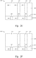
Figure 2D , adielectric material 208 is formed betweenadjacent features 206. In one embodiment, thedielectric material 208 and thefeatures 206 are coplanar at the end of the deposition process of thedielectric material 208. In another embodiment, thedielectric material 208 is also formed on thefeatures 206 and thegate electrode 110. Thedielectric material 208 may be the same material as thedielectric material 104. In one embodiment, thedielectric material 208 is silicon oxide and is deposited by a flowable chemical vapor deposition (FCVD) process. A chemical mechanical planarization (CMP) process is then performed on thedielectric material 208 to expose thefeatures 206, as shown inFigure 2E . Asurface 210 of eachfeature 206 is exposed, and thesurfaces 210 are coplanar with asurface 212 of thedielectric material 208. - Next, as shown in
Figure 2F , thefeatures 206 are removed to expose thesurfaces 202 of the remainingportions 204. Thegate dielectric 108 and thegate electrode 110 should appear in the background but are omitted for clarity. Thefeatures 206 may be removed by a selective etching process so thedielectric material 208 is not substantially affected. In other words, the etch rate of thefeature 206 is much faster than the etch rate of thedielectric material 208 since thefeature 206 and thedielectric material 208 are made of different materials. The process for etching is described below. As a result of the removal process, a plurality ofopenings 214, such as trenches or vias, is formed in thedielectric material 208. Eachopening 214 has the same shape as thefeature 206. Afill material 216, such as a stressor material, is then deposited in eachopening 214 on thesurface 202 of the remainingportion 204 of eachfin 102, as shown inFigure 2G . Thefill material 216 may be also deposited on thesurface 212 of thedielectric material 208, and an etch back process may be performed to remove thefill material 216 deposited on thesurface 212 of thedielectric material 208. Thefill material 216 may be the source or drain of a FinFET device and may be a silicon and/or germanium based material. In one embodiment, thefill material 216 is an electrically conductive material. Thefill material 216 may be formed by an epitaxial deposition process in an epitaxial deposition chamber available from Applied Materials, Inc. The epitaxial deposition process is generally performed by flowing epitaxy precursors such as silane, germane, phosphine, and arsine into the epitaxial deposition chamber and heating the substrate to a temperature, for example 300 degrees Celsius to 600 degrees Celsius, that results in epitaxial deposition on the substrate. For the Group III-V semiconductor materials, precursors for the Group III elements include halides, which can be reacted with materials such as arsine, phosphine, and stilbene. In one embodiment, thefill material 216 is silicon doped with phosphorus and the FinFET device is an n-type FET. In another embodiment, thefill material 216 is silicon germanium doped with boron or gallium, and the FinFET device is a p-type FET. The shape of thefill material 216 is constrained by theopening 214 that thefill material 216 is formed therein. Thus, instead of having a diamond shape, thefill material 216 has a rectangular cross-section, and the distance betweenadjacent fill materials 216 is increased. Eachfill material 216 has asurface 213 that is recessed from thesurface 212 of thedielectric material 208. - Another benefit of forming the plurality of
openings 214 is that any material deposited on thesurface 213 of thefill material 216 within theopening 214 is self-aligned. In one embodiment, ametal contact 222 is deposited over thefill material 216 within theopening 214, as shown inFigure 2H . Themetal contact 222 is self-aligned to thefill material 216, i.e., a source or drain, since both themetal contact 222 and thefill material 216 are formed within theopening 214. Themetal contact 222 may be fabricated from a metal such as cobalt or tungsten. Additional materials may be formed on thefill material 216 prior to the deposition of themetal contact 222. For example, a silicide orgermanide layer 218 may be formed on thefill material 216 by a silicidation process. Aliner 220 may be formed conformally in theopening 214 by an atomic layer deposition (ALD) process. Themetal contact 222 is then deposited on theliner 220. A CMP process may be performed to planarize the surface. - In some embodiments, one suitable apparatus for performing the etching process is the CENTURA™ RP Epi platform available from Applied Materials, Inc., Santa Clara, CA. It is contemplated that other suitably configured apparatus from other manufacturers may also be utilized in accordance with the embodiments described herein. As aforementioned, selective etching is utilized to remove the III-V structures. For example, etch chemistries selective to III-V materials are utilized to remove the
features 206 preferentially to the oxide and/or nitride containing gap fill material. The etching operation may be performed in the same chamber as the deposition operation. - In some embodiments, a chlorine containing gas, such as HCI, is used as an etchant. The chlorine containing gas is optionally delivered to a substrate processing environment with a hydrogen containing gas, such as H2. In some embodiments, the chlorine containing gas is optionally delivered to a substrate processing environment with a relatively nonreactive carrier gas such as N2 or Ar. In one example, the HCI is delivered to the substrate processing environment at a flow rate of between about 1 sccm and about 500 sccm, for a 300 mm wafer. The nonreactive carrier gas is delivered to the substrate processing environment at a flow rate of between about 1 slm and about 20 slm. A temperature of the wafer is maintained between about 300°C and about 800°C and a pressure of the substrate processing environment is maintained between about 0 Torr and about 100 Torr.
- HCl is used instead of a mixture of HCl and H2O because H2O oxidizes the surface of the silicon surfaces. Using an HCl etch gas with a mass flow of 1-500 sccm at low temperatures (less than about 800°C) reduces the damage to the Si, SiOx and SiNx materials. Moreover, using low pressure etch processes (less than about 100 Torr) allows the gas to reach the bottom of the deep trenches of the high aspect ratio features.
-
Figures 3A - 3C illustrate a process for forming a semiconductor device according to another embodiment described herein.Figure 3A is a side view of thesemiconductor structure 300. Thesemiconductor structure 300 includes asubstrate 302 having asemiconductor surface 305. Thesemiconductor surface 305 includes a plurality of exposedportions 304 separated by a plurality of coveredportions 306. In one embodiment, thesubstrate 302 is a silicon substrate, and thesemiconductor surface 305 is a silicon surface. A firstdielectric material 308 is disposed on the coveredportions 306 of thesemiconductor surface 305. The firstdielectric material 308 may be silicon oxide, silicon nitride, silicon oxynitride, silicon carbonitride, or any other suitable dielectric material. Next, as shown inFigure 3B , afeature 310 is formed on each exposedportion 304 of thesemiconductor surface 305. Thefeatures 310 may be the same as thefeatures 206. Prior to forming thefeatures 310, any native oxides formed on thesemiconductor surface 305 may be removed by a pre-clean process. Thefeatures 310 may be formed in an epitaxial deposition chamber. In one embodiment, eachfeature 310 is formed in by first forming a nucleation layer on a corresponding exposedportion 304 of thesemiconductor surface 305. The nucleation layer and thefeatures 310 may be formed under the same process conditions as the nucleation layer and thefeatures 206. Unlike the silicon or germanium based materials, which form a diamond shape due to the different growth rate on different surface planes, the materials used to form thefeatures 310 do not form a diamond shape. The height, width and facets of thefeatures 310 can be controlled by temperature, pressure and/or precursor flow. - Next, as shown in
Figure 3C , a seconddielectric material 312 is formed betweenadjacent features 310. In one embodiment, the seconddielectric material 312 and thefeatures 310 are coplanar at the end of the deposition process of the seconddielectric material 312. In another embodiment, the seconddielectric material 312 is also formed on thefeatures 310 and a CMP process is performed on the seconddielectric material 312 to expose thefeatures 310. The seconddielectric material 312 may be the same material as thedielectric material 208. - Process operations shown in
Figures 2F ,2G and 2H are then performed on thesemiconductor structure 300 to form a plurality of openings in the seconddielectric material 312, to deposit a fill material in the plurality of openings, and to deposit a metal in the plurality of openings. The fill material may be the same as thefill material 216, and the metal may be the same as themetal contact 222. The fill material and the metal are self-aligned since both materials are formed within the same opening. - A fin structure processing method is described herein, and is described above.
Figure 4A illustrates operations of amethod 400 for fin structure processing according to some embodiments. Themethod 400 includes removing a portion of a first fin of a plurality of fins formed on a semiconductor substrate to expose a surface of a remaining portion of the first fin, wherein the fins are adjacent to dielectric material structures formed on the semiconductor substrate atoperation 402.Method 400 further includes forming features on the surface of the remaining portion of the first fin by depositing a Group III-V semiconductor material in a substrate processing environment atoperation 404. Themethod 400 further includes etching the features with an etching gas to form a plurality of openings between adjacent dielectric material structures atoperation 408. In some embodiments, the etching gas is a chlorine containing gas. In some embodiments, the etching gas is delivered to the substrate processing environment with a hydrogen containing gas and/or a carrier gas, as described above. - A fin structure processing method is described herein, and is described above.
Figure 4B illustrates operations of amethod 420 for fin structure processing according to some embodiments. Themethod 420 includes removing a portion of a first fin of a plurality of fins formed on a semiconductor substrate to expose a surface of a remaining portion of the first fin, wherein the fins are adjacent to dielectric material structures formed on the semiconductor substrate atoperation 402.Method 420 further includes forming features on the surface of the remaining portion of the first fin by depositing a Group III-V semiconductor material in a substrate processing environment atoperation 404. Themethod 420 further includes planarizing the Group III-V semiconductor material by a chemical mechanical polishing process (CMP) atoperation 406. Themethod 420 further includes etching the features with an etching gas to form a plurality of openings between adjacent dielectric material structures atoperation 408. In some embodiments, the etching gas is a chlorine containing gas. In some embodiments, the etching gas is delivered to the substrate processing environment with a hydrogen containing gas and/or a carrier gas. Themethod 420 further includes forming a fill material on the surface of the remaining portion of the first fin, wherein the fill material is formed within a corresponding opening of the plurality of openings atoperation 412. - A fin structure processing method is described herein, and is described above.
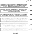
Figure 4C illustrates operations of amethod 430 for fin structure processing according to some embodiments. Themethod 430 includes removing a portion of a first fin of a plurality of fins formed on a semiconductor substrate to expose a surface of a remaining portion of the first fin, wherein the fins are adjacent to dielectric material structures formed on the semiconductor substrate atoperation 402.Method 430 further includes forming features on the surface of the remaining portion of the first fin by depositing a Group III-V semiconductor material in a substrate processing environment atoperation 404. Themethod 430 further includes planarizing the Group III-V semiconductor material by a chemical mechanical polishing process atoperation 406. Themethod 430 further includes etching the features with an etching gas to form a plurality of openings between adjacent dielectric material structures atoperation 408. In some embodiments, the etching gas is a chlorine containing gas. Themethod 430 delivering a hydrogen containing gas, a carrier gas, or a combination thereof to the substrate processing environment atoperation 410. Themethod 430 further includes forming a fill material on the surface of the remaining portion of the first fin, wherein the fill material is formed within a corresponding opening of the plurality of openings atoperation 412. - In some embodiments, the III-V growth chamber is connected to a chamber abatement apparatus. The chamber abatement apparatus includes an absorber that can be used for abatement of a species, such as an arsenic containing material. The chamber abatement apparatus allows removing arsenic, for example, from the effluent stream flowing from the substrate processing chamber. Conventional etch tools do not have a dedicated abatement apparatus. Therefore, unlike conventional etch tools, the use of the III-V growth chamber for etch avoids contamination and abatement issues because the III-V growth chamber is equipped with a chamber abatement apparatus that is connected to the effluent flowing from the substrate processing chamber.
- Therefore and in some embodiments the
method 400 includes removing a species (such as an arsenic containing material) from an effluent stream flowing from the substrate processing chamber by a chamber abatement apparatus atoperation 414. In some embodiments, the chamber abatement apparatus includes an absorber. - While the foregoing is directed to embodiments of the disclosure, other and further embodiments may be devised without departing from the basic scope thereof, and the scope thereof is determined by the claims that follow.
Claims (15)
- A fin structure processing method, comprising:removing a portion of a first fin of a plurality of fins formed on a substrate to expose a surface of a remaining portion of the first fin, wherein the fins are adjacent to dielectric material structures formed on the substrate;performing a deposition operation to form features on the surface of the remaining portion of the first fin by depositing a Group III-V semiconductor material in a substrate processing environment; andperforming an etching operation to etch the features with an etching gas to form a plurality of openings between adjacent dielectric material structures, wherein the etching operation is performed in the same chamber as the deposition operation.
- The method of claim 1, further comprising planarizing the Group III-V semiconductor material by a chemical mechanical polishing process.
- The method of any of claims 1 or 2, wherein the substrate processing environment is an epitaxial deposition chamber.
- The method of any of claims 1 to 3, wherein the etching gas is a chlorine containing gas.
- The method of claim 4, wherein the chlorine containing gas is HCI.
- The method of any of claims 1 to 5, further comprising forming a fill material on the surface of the remaining portion of the first fin, wherein the fill material is formed within a corresponding opening of the plurality of openings.
- The method of any of claims 1 to 6, wherein a temperature of the substrate is between about 300°C and about 800°C, and a pressure of the substrate processing environment is between about 1 Torr and about 100 Torr during at least a portion of the etching operation.
- The method of any of claims 1 to 7, wherein the etching gas is delivered to the substrate processing environment at a flow rate of between about 1 sccm and about 500 sccm, for a 300 mm wafer.
- The method of any of claims 1 to 8, wherein the etching gas is delivered to the substrate processing environment with a hydrogen containing gas, a carrier gas, or combinations thereof.
- The method of claim 9, wherein the carrier gas is N2 or Ar.
- The method of any of claims 9 to 10, wherein the carrier gas is delivered to the substrate processing environment at a flow rate of between about 1 slm and about 20 slm.
- The method of any of claims 1 to 11, further comprising removing a species from an effluent stream flowing from the substrate processing environment by a chamber abatement apparatus.
- A fin structure processing method, comprising:removing a portion of a first fin of a plurality of fins formed on a substrate to expose a surface of a remaining portion of the first fin, wherein the fins are adjacent to dielectric material structures formed on the substrate;performing a deposition operation to form features on the surface of the remaining portion of the first fin by depositing a Group III-V semiconductor material in a substrate processing environment;planarizing the Group III-V semiconductor material by a chemical mechanical polishing process;performing an etching operation to etch the features with an etching gas to form a plurality of openings between adjacent dielectric material structures, wherein the etching operation is performed in the same chamber as the deposition operation; andforming a fill material on the surface of the remaining portion of the first fin, wherein the fill material is formed within a corresponding opening of the plurality of openings.
- The method of claim 13, wherein the features are formed in an epitaxial deposition chamber.
- A fin structure processing method, comprising:removing a portion of a first fin of a plurality of fins formed on a substrate to expose a surface of a remaining portion of the first fin, wherein the fins are adjacent to dielectric material structures formed on the substrate;performing a deposition operation to form features on the surface of the remaining portion of the first fin by depositing a Group III-V semiconductor material in a substrate processing environment;planarizing the Group III-V semiconductor material by a chemical mechanical polishing process;performing an etching operation to etch the features with an etching gas to form a plurality of openings between adjacent dielectric material structures, wherein the etching operation is performed in the same chamber as the deposition operation and wherein the etching gas is HCI;delivering a hydrogen containing gas, a carrier gas, or a combination thereof, to the substrate processing environment; and
forming a fill material on the surface of the remaining portion of the first fin, wherein the fill material is formed within a corresponding opening of the plurality of openings.
Applications Claiming Priority (1)
| Application Number | Priority Date | Filing Date | Title |
|---|---|---|---|
| US201862662008P | 2018-04-24 | 2018-04-24 |
Publications (1)
| Publication Number | Publication Date |
|---|---|
| EP3561878A1 true EP3561878A1 (en) | 2019-10-30 |
Family
ID=66334182
Family Applications (1)
| Application Number | Title | Priority Date | Filing Date |
|---|---|---|---|
| EP19168988.4A Withdrawn EP3561878A1 (en) | 2018-04-24 | 2019-04-12 | Method to remove iii-v materials in high aspect ratio structures |
Country Status (5)
| Country | Link |
|---|---|
| EP (1) | EP3561878A1 (en) |
| JP (1) | JP2019192913A (en) |
| KR (1) | KR102182035B1 (en) |
| CN (1) | CN110400747A (en) |
| TW (1) | TW201946112A (en) |
Cited By (1)
| Publication number | Priority date | Publication date | Assignee | Title |
|---|---|---|---|---|
| US12237229B2 (en) | 2020-05-28 | 2025-02-25 | Taiwan Semiconductor Manufacturing Co., Ltd. | Shallow trench isolation structures having uniform step heights |
Citations (4)
| Publication number | Priority date | Publication date | Assignee | Title |
|---|---|---|---|---|
| US20140273398A1 (en) * | 2013-03-13 | 2014-09-18 | Taiwan Semiconductor Manufacturing Company, Ltd. | Methods for Forming Semiconductor Materials in STI Trenches |
| US20160149036A1 (en) * | 2014-11-25 | 2016-05-26 | Taiwan Semiconductor Manufacturing Company, Ltd. | Source/drain structure and manufacturing the same |
| WO2016190858A1 (en) * | 2015-05-27 | 2016-12-01 | Intel Corporation | Apparatus and methods to create a buffer which extends into a gated region of a transistor |
| US20180033873A1 (en) * | 2016-07-29 | 2018-02-01 | Applied Materials, Inc. | Method of uniform channel formation |
Family Cites Families (8)
| Publication number | Priority date | Publication date | Assignee | Title |
|---|---|---|---|---|
| US8723236B2 (en) * | 2011-10-13 | 2014-05-13 | Taiwan Semiconductor Manufacturing Company, Ltd. | FinFET device and method of manufacturing same |
| US9029246B2 (en) * | 2013-07-30 | 2015-05-12 | Taiwan Semiconductor Manufacturing Company, Ltd. | Methods of forming epitaxial structures |
| US9159833B2 (en) * | 2013-11-26 | 2015-10-13 | Taiwan Semiconductor Manufacturing Company, Ltd. | Fin structure of semiconductor device |
| CN105097517B (en) * | 2014-04-25 | 2018-07-20 | 中芯国际集成电路制造(上海)有限公司 | A kind of FinFET and its manufacturing method, electronic device |
| US9209279B1 (en) * | 2014-09-12 | 2015-12-08 | Applied Materials, Inc. | Self aligned replacement fin formation |
| TWI791199B (en) * | 2015-05-11 | 2023-02-01 | 美商應用材料股份有限公司 | Horizontal gate all around and finfet device isolation |
| US11017999B2 (en) * | 2016-10-05 | 2021-05-25 | International Business Machines Corporation | Method and structure for forming bulk FinFET with uniform channel height |
| US10008601B2 (en) * | 2016-10-17 | 2018-06-26 | International Business Machines Corporation | Self-aligned gate cut with polysilicon liner oxidation |
-
2019
- 2019-04-10 TW TW108112467A patent/TW201946112A/en unknown
- 2019-04-12 EP EP19168988.4A patent/EP3561878A1/en not_active Withdrawn
- 2019-04-22 KR KR1020190046850A patent/KR102182035B1/en not_active Expired - Fee Related
- 2019-04-23 JP JP2019081708A patent/JP2019192913A/en active Pending
- 2019-04-23 CN CN201910331618.9A patent/CN110400747A/en active Pending
Patent Citations (4)
| Publication number | Priority date | Publication date | Assignee | Title |
|---|---|---|---|---|
| US20140273398A1 (en) * | 2013-03-13 | 2014-09-18 | Taiwan Semiconductor Manufacturing Company, Ltd. | Methods for Forming Semiconductor Materials in STI Trenches |
| US20160149036A1 (en) * | 2014-11-25 | 2016-05-26 | Taiwan Semiconductor Manufacturing Company, Ltd. | Source/drain structure and manufacturing the same |
| WO2016190858A1 (en) * | 2015-05-27 | 2016-12-01 | Intel Corporation | Apparatus and methods to create a buffer which extends into a gated region of a transistor |
| US20180033873A1 (en) * | 2016-07-29 | 2018-02-01 | Applied Materials, Inc. | Method of uniform channel formation |
Cited By (1)
| Publication number | Priority date | Publication date | Assignee | Title |
|---|---|---|---|---|
| US12237229B2 (en) | 2020-05-28 | 2025-02-25 | Taiwan Semiconductor Manufacturing Co., Ltd. | Shallow trench isolation structures having uniform step heights |
Also Published As
| Publication number | Publication date |
|---|---|
| KR20190123691A (en) | 2019-11-01 |
| CN110400747A (en) | 2019-11-01 |
| KR102182035B1 (en) | 2020-11-23 |
| TW201946112A (en) | 2019-12-01 |
| JP2019192913A (en) | 2019-10-31 |
Similar Documents
| Publication | Publication Date | Title |
|---|---|---|
| US11901452B2 (en) | Source/drain structure having multi-facet surface | |
| TWI821415B (en) | Semiconductor device and method for forming the same | |
| US11961768B2 (en) | CMOS FinFET structures including work-function materials having different proportions of crystalline orientations and methods of forming the same | |
| US12249650B2 (en) | FinFET device and methods of forming the same | |
| US11894464B2 (en) | Fin field-effect transistor device with composite liner for the Fin | |
| TWI745045B (en) | Semiconductor device and method | |
| US10269647B2 (en) | Self-aligned EPI contact flow | |
| US10867860B2 (en) | Methods of forming FinFET device | |
| US10256317B2 (en) | Vertical transistor gated diode | |
| TWI881584B (en) | Semiconductor devices and methods of fabricating the same | |
| KR102182035B1 (en) | Method to remove iii-v materials in high aspect ratio structures | |
| US10770568B2 (en) | Method to remove III-V materials in high aspect ratio structures | |
| US12414320B2 (en) | Fin field-effect transistor device with composite liner for the fin | |
| US20240250154A1 (en) | Fin field-effect transistor and method of forming the same |
Legal Events
| Date | Code | Title | Description |
|---|---|---|---|
| PUAI | Public reference made under article 153(3) epc to a published international application that has entered the european phase |
Free format text: ORIGINAL CODE: 0009012 |
|
| STAA | Information on the status of an ep patent application or granted ep patent |
Free format text: STATUS: THE APPLICATION HAS BEEN PUBLISHED |
|
| AK | Designated contracting states |
Kind code of ref document: A1 Designated state(s): AL AT BE BG CH CY CZ DE DK EE ES FI FR GB GR HR HU IE IS IT LI LT LU LV MC MK MT NL NO PL PT RO RS SE SI SK SM TR |
|
| AX | Request for extension of the european patent |
Extension state: BA ME |
|
| STAA | Information on the status of an ep patent application or granted ep patent |
Free format text: STATUS: REQUEST FOR EXAMINATION WAS MADE |
|
| 17P | Request for examination filed |
Effective date: 20200428 |
|
| RBV | Designated contracting states (corrected) |
Designated state(s): AL AT BE BG CH CY CZ DE DK EE ES FI FR GB GR HR HU IE IS IT LI LT LU LV MC MK MT NL NO PL PT RO RS SE SI SK SM TR |
|
| STAA | Information on the status of an ep patent application or granted ep patent |
Free format text: STATUS: THE APPLICATION IS DEEMED TO BE WITHDRAWN |
|
| 18D | Application deemed to be withdrawn |
Effective date: 20211103 |