EP3561158B1 - Method for growing single crystal silicon carbide ingot having large diameter - Google Patents
Method for growing single crystal silicon carbide ingot having large diameter Download PDFInfo
- Publication number
- EP3561158B1 EP3561158B1 EP17882910.7A EP17882910A EP3561158B1 EP 3561158 B1 EP3561158 B1 EP 3561158B1 EP 17882910 A EP17882910 A EP 17882910A EP 3561158 B1 EP3561158 B1 EP 3561158B1
- Authority
- EP
- European Patent Office
- Prior art keywords
- seed crystal
- protective layer
- single crystal
- ingot
- layer
- Prior art date
- Legal status (The legal status is an assumption and is not a legal conclusion. Google has not performed a legal analysis and makes no representation as to the accuracy of the status listed.)
- Active
Links
Images





Classifications
-
- C—CHEMISTRY; METALLURGY
- C30—CRYSTAL GROWTH
- C30B—SINGLE-CRYSTAL GROWTH; UNIDIRECTIONAL SOLIDIFICATION OF EUTECTIC MATERIAL OR UNIDIRECTIONAL DEMIXING OF EUTECTOID MATERIAL; REFINING BY ZONE-MELTING OF MATERIAL; PRODUCTION OF A HOMOGENEOUS POLYCRYSTALLINE MATERIAL WITH DEFINED STRUCTURE; SINGLE CRYSTALS OR HOMOGENEOUS POLYCRYSTALLINE MATERIAL WITH DEFINED STRUCTURE; AFTER-TREATMENT OF SINGLE CRYSTALS OR A HOMOGENEOUS POLYCRYSTALLINE MATERIAL WITH DEFINED STRUCTURE; APPARATUS THEREFOR
- C30B23/00—Single-crystal growth by condensing evaporated or sublimed materials
- C30B23/02—Epitaxial-layer growth
- C30B23/025—Epitaxial-layer growth characterised by the substrate
-
- C—CHEMISTRY; METALLURGY
- C30—CRYSTAL GROWTH
- C30B—SINGLE-CRYSTAL GROWTH; UNIDIRECTIONAL SOLIDIFICATION OF EUTECTIC MATERIAL OR UNIDIRECTIONAL DEMIXING OF EUTECTOID MATERIAL; REFINING BY ZONE-MELTING OF MATERIAL; PRODUCTION OF A HOMOGENEOUS POLYCRYSTALLINE MATERIAL WITH DEFINED STRUCTURE; SINGLE CRYSTALS OR HOMOGENEOUS POLYCRYSTALLINE MATERIAL WITH DEFINED STRUCTURE; AFTER-TREATMENT OF SINGLE CRYSTALS OR A HOMOGENEOUS POLYCRYSTALLINE MATERIAL WITH DEFINED STRUCTURE; APPARATUS THEREFOR
- C30B29/00—Single crystals or homogeneous polycrystalline material with defined structure characterised by the material or by their shape
- C30B29/10—Inorganic compounds or compositions
- C30B29/36—Carbides
Definitions
- the following embodiments relate to a process for preparing a seed crystal with a protective layer.
- a single crystal of silicon carbide (SiC), silicon (Si), gallium nitride (GaN), sapphire (Al 2 O 3 ), gallium arsenide (GaAs), aluminum nitride (AlN), or the like has characteristics that cannot be expected from a polycrystal counterpart thereof.
- SiC silicon carbide
- Si silicon
- GaN gallium nitride
- Al 2 O 3 sapphire
- GaAs gallium arsenide
- AlN aluminum nitride
- single crystal silicon carbide (SiC) has a large energy band gap and is excellent in maximum break field voltage and thermal conductivity as compared with silicon (Si).
- the carrier mobility of single crystal silicon carbide is comparable to that of silicon, and the saturation drift rate of electrons and the breakdown voltage thereof are large as well.
- Japanese Laid-open Patent Publication No. 2001-114599 discloses a method of growing a single crystal ingot on a seed crystal by maintaining the seed crystal at a temperature lower than that of a raw material powder by 10 to 100°C while heating it with a heater in a vacuum container (or a heating furnace) capable of introducing argon gas.
- US 2013/171403 A1 teaches a method for producing an SiC volume monocrystal by sublimation growth.
- CN 101 985 773 B discloses a seed crystal treatment method for silicon carbide growth and a silicon carbide mono-crystal growing method using the same.
- Another seed crystal processing method for silicon carbide single crystal growth is provided in CN 106 757 321 A .
- a step of adhering a seed crystal is generally carried out in advance.
- an adhesive (150) is applied between a seed crystal holder (190) and a seed crystal (110), which are pressed to adhere the seed crystal.
- a raw material (300) is heated and sublimated in a reaction vessel (200), whereby a single crystal ingot is grown on the front side of the seed crystal (110).
- Disclosed herein, but not claimed, is a process for growing a single crystal ingot without adhesion of a seed crystal to a holder, thereby growing an SiC single crystal ingot having a large diameter and high quality.
- the present invention provides a process for preparing a seed crystal provided with a protective layer for use in the above process.
- a process for preparing a seed crystal provided with a protective layer which comprises molding a composition that comprises a binder resin into a sheet form to prepare a protective layer;
- a cured and carbonaceous protective layer is formed on the rear side of a seed crystal of a silicon carbide single crystal.
- the protective layer has a protrusion member that protrudes outward from the periphery of the seed crystal.
- the process for preparing a seed crystal provided with a protective layer comprises molding a composition that comprises a binder resin into a sheet form to prepare a protective layer;
- the process for preparing a seed crystal provided with a protective layer comprises (a1) preparing a composition that comprises a binder resin and a filler; and (a2) coating the composition on the rear side of a seed crystal of an SiC single crystal and thermally treating the coated composition to form a carbonaceous protective layer, wherein the carbonaceous protective layer has a thickness of 5 to 1,000 ⁇ m, and the filler is a carbon-based filler, a metal-based filler, or a composite filler thereof.
- the filler added in the preparation of a carbonaceous protective layer prevents cracks or the like that may be generated in the protective layer during the thermal treatment.
- step (a1) a composition that comprises a binder resin and a filler is prepared.
- the binder resin is the main component of a coating layer for the preparation of a protective layer.
- the binder resin may be, for example, a phenolic resin, a polyacrylonitrile resin, a pitch-based resin, a polyvinyl chloride resin, a polyacrylic acid resin, a furan-based resin, an epoxy-based resin, or a mixed resin thereof.
- the binder resin has a high actual carbon ratio.
- the binder resin may have an actual carbon ratio of 5 to 50% or 10 to 30% in an inert gas atmosphere.
- the binder resin is preferably a curable resin.
- it may be a thermosetting resin.
- the filler serves to promote carbonization or graphitization during the thermal treatment after the formation of a coating layer and to prevent cracks from being generated due to an excessive shrinkage.
- the filler may be, for example, a carbon-based filler, a metal-based filler, or a composite filler thereof.
- the filler may comprise a component such as flake graphite, amorphous graphite, expanded graphite, carbon black, carbon nanotubes, graphene, tantalum (Ta), tungsten (W), rhenium (Re), molybdenum (Mo), hafnium (Hf), tantalum carbide (TaC), tungsten carbide (WC), and the like.
- the filler may be employed in an amount of 5 to 95% by weight, 5 to 60% by weight, 10 to 50% by weight, or 20 to 40% by weight, based on the total weight of the composition.
- the filler may be employed in the composition in an amount of 10 to 200 parts by weight or 30 to 150 parts by weight per 100 parts by weight of the binder resin. If the content of the filler is within the above preferable ranges, it may be more advantageous in preventing shrinkage and cracks, which may be generated during the thermal treatment after the formation of a coating layer, to thereby form a protective layer having an excellent surface.
- the composition is preferably a liquid composition for the efficiency of coating.
- the composition may comprise a solvent such as ethanol, methanol, acetone, dimethylformamide (DMF), dimethylsulfoxide (DMSO), and the like.
- a solvent such as ethanol, methanol, acetone, dimethylformamide (DMF), dimethylsulfoxide (DMSO), and the like.
- the solids content of the liquid composition may be 10 to 90% by weight or 20 to 50% by weight.
- composition may further comprise a wetting dispersant, a defoaming agent, or the like.
- composition is coated on the rear side (112) of a seed crystal (110) of an SiC single crystal to obtain a coating layer (120'), which is then carbonized or graphitized by thermal treatment to form a carbonaceous protective layer (120).
- the "front side” of a seed crystal refers to one of the two sides of the seed crystal generally having a wide and flat shape on which a single crystal ingot grows.
- the “rear side” of a seed crystal refers to the opposite side of the seed crystal to the side on which a single crystal ingot grows.
- an adhesive is applied to the rear side of a seed crystal, which is then attached to a holder.
- a protective layer is formed on the rear side of a seed crystal, which is not attached to a holder.
- any seed crystal having various crystal structures such as 4H-SiC, 6H-SiC, 3C-SiC, and 15R-SiC may be used depending on the kind of crystals to be grown.
- the seed crystal may be subjected to cleaning prior to the coating.
- a silicon dioxide layer may be formed on the surface of a seed crystal by a reaction of silicon with oxygen. It is preferable that such an oxide layer is removed in advance by cleaning since it may have the seed crystal detached or may cause defects when a single crystal ingot is grown in the subsequent process.
- the cleaning may be carried out with acetone, alcohol, distilled water, an acid solution, or the like, and may be carried out by ultrasonic treatment or immersion. It may be performed once, twice, or more.
- the coating is carried out on the rear side of the seed crystal.
- a conventional coating method such as spin coating and tape casting may be used for the coating.
- the coating may be carried out in a thickness range of 10 to 2,000 ⁇ m or in a thickness range of 20 to 1,500 ⁇ m. If the coating thickness is too smaller than the above preferable range, there is a possibility that the protective layer upon the thermal treatment may not serve as a protective layer. On the other hand, if it is too large, bubbles or cracks may be generated, or the coating layer may be peeled off, upon the thermal treatment.
- the coating layer is dried and cured at a temperature of 30 to 300°C or at a temperature of 50 to 200°C, followed by thermal treatment at a temperature of 300°C or higher, for example, 300 to 2,200°C to form a carbonaceous protective layer through carbonization thereof.
- the binder resin contained in the composition is carbonized or graphitized by the thermal treatment to form a carbonaceous protective layer.
- the filler in the coating layer may prevent cracks that may be generated during the thermal treatment and promote the carbonization or graphitization.
- the temperature of thermal treatment may be 400°C or higher, 500°C or higher, or 600°C or higher, for example, 400 to 1,500°C, 500 to 1,000°C, 1,500 to 2,500°C, or 2,000 to 2,500°C.
- the thermal treatment may be carried out for 1 to 10 hours or 1 to 5 hours.
- the thermal treatment may be carried out under the conditions of a temperature elevation rate of 0.5 to 5°C/min and a temperature of 500°C or higher or 600°C or higher.
- a temperature elevation rate of 0.5 to 5°C/min and a temperature of 500°C or higher or 600°C or higher.
- it may be carried out by raising the temperature to 500 to 1000°C, maintaining the temperature for 1 to 5 hours for heating, and then lowering the temperature at a rate of 0.5 to 5°C/min.
- the thermal treatment may be carried out under the conditions of a temperature elevation rate of 1 to 5°C/min and a temperature of 1,500°C or higher or 2,000°C or higher.
- a temperature elevation rate of 1 to 5°C/min and a temperature of 1,500°C or higher or 2,000°C or higher.
- it may be carried out by raising the temperature to 1,500 to 2,500°C or 2,000 to 2,500°C, maintaining the temperature for 1 to 5 hours for heating, and then lowering the temperature at a rate of 1 to 5°C/min.
- the thermal treatment may be carried out in an inert gas atmosphere.
- it may be carried out in an argon gas or nitrogen gas atmosphere.
- the thermal treatment may be carried out by induction heating or by resistance heating. That is, the thermal treatment may be carried out in an induction heating furnace or in a resistance heating furnace.
- the process for preparing a seed crystal provided with a protective layer comprises (c1) molding a composition that comprises a binder resin into a sheet form to prepare a protective layer; (c2) cutting the protective layer and attaching it to the rear side of a seed crystal of a silicon carbide (SiC) single crystal by pressure thereon; and (c3) curing and carbonizing the protective layer attached to the seed crystal, wherein the protective layer has a diameter larger than that of the seed crystal, whereby it covers the entire rear side of the seed crystal and has a protrusion member that protrudes outward from the periphery of the seed crystal.
- a carbonaceous protective layer is formed on the rear side of a seed crystal.
- the protective layer in a sheet form is prepared in advance and then attached to the seed crystal, rather than it is directly formed on the surface of the seed crystal.
- this process can prepare a protective layer that has a diameter larger than that of a seed crystal.
- the protrusion member of the protective layer is used as a support for a seed crystal when it is placed in a reaction vessel.
- it is possible to obtain an ingot having a large diameter by preventing the diameter thereof from being reduced during the growth of an SiC single crystal ingot while producing an effect similar to the case where a seed crystal holder is used, even though the conventional method in which a seed crystal is attached to a seed crystal holder is not adopted.
- the seed crystal does not need to be in direct contact with the reaction vessel, which is a heating body, the loss and contamination of the seed crystal can be suppressed.
- Fig. 4 shows a method of forming a protective layer on a seed crystal according to the embodiment.
- Fig. 5 shows a method of attaching a protective layer to a seed crystal according to still the embodiment.
- step (c1) a composition that comprises a binder resin is molded into a sheet form to prepare a protective layer.
- the binder resin is the main component of a coating composition for the preparation of a protective layer.
- the resins as exemplified in the above embodiment may be used as the binder resin.
- the composition may further comprise a filler in addition to the binder resin.
- the filler serves to promote carbonization during the thermal treatment after the coating of the composition and to prevent cracks from being generated due to an excessive shrinkage.
- the filler may be, as exemplified in the above embodiment, a carbon-based filler, a metal-based filler, or a composite filler thereof.
- the filler may be employed in the composition in an amount of 10 to 200 parts by weight or 30 to 150 parts by weight per 100 parts by weight of the binder resin. If the content of the filler is within the above preferable range, it may be more advantageous in preventing shrinkage and cracks, which may be generated during the thermal treatment after the formation of a coating layer, to thereby form a protective layer having an excellent surface.
- a phenolic resin may be used as the binder resin
- graphite may be used as the filler
- the composition may comprise 50 to 120 parts by weight of the filler per 100 parts by weight of the binder resin.
- the composition may further comprise a solvent for controlling the viscosity thereof when it is molded.
- the composition may comprise a solvent such as ethanol, methanol, acetone, dimethylformamide (DMF), dimethylsulfoxide (DMSO), and the like.
- the solids content of the composition may be 10 to 90% by weight or 20 to 50% by weight.
- composition may further comprise a wetting dispersant, a defoaming agent, or the like.
- the composition thus prepared is molded into a sheet form to prepare a protective layer.
- the molding may be carried out using such a process as roll coating, comma coating, dip coating, and the like.
- the molding into a sheet form may be carried out in a thickness range of 10 to 3,000 ⁇ m or in a thickness range of 100 to 1,000 ⁇ m. If the molding thickness is too smaller than the above preferable range, there is a possibility that the tensile strength of the protective layer may be low and that the protective layer upon the thermal treatment may not serve as a protective layer. On the other hand, if it is too large, bubbles or cracks may be generated, or the coating layer may be peeled off, upon the thermal treatment.
- the release film serves to prevent the problem that the surface of the protective layer is contaminated during the molding process or that the composition, which is not dried yet, comes into contact with the equipment thereby impairing the processability.
- the release film may be a conventional release film.
- it may be a PET film coated with silicone, a paper film coated with silicon, or the like.
- the release film may have a thickness of 25 to 100 ⁇ m.
- the release film may have a peel strength of 3 to 30 gf/inch.
- the molding of the protective layer may be carried out as a single layer or a multilayer.
- the above composition only may be molded into a sheet form to prepare a protective layer.
- the composition may be coated on a core layer (i.e., a separate substrate), which is then molded into a sheet form to prepare a protective layer.
- a core layer i.e., a separate substrate
- the composition may be coated on both sides of a core layer composed of a fibrous material, which is then molded into a sheet form to prepare a protective layer.
- a core layer of a fibrous material As a core layer of a fibrous material is used as described above, it is possible to readily form a thick protective layer, and it is more advantages in achieving a uniform thickness and layer quality.
- the strength of the protective layer is increased to prevent the seed crystal from vanishing or peeling off when a single crystal ingot is grown, and it may be more effective to prevent deformation of the seed crystal by suppressing shrinkage of the protective layer.
- the core layer of a fibrous material may, more specifically, comprise cellulose, rayon, carbon fiber, or the like.
- the core layer may be composed of a cellulose fiber.
- the core layer may increase the tensile strength of the protective layer, thereby improving the supporting force thereof when a seed crystal is placed in a reaction vessel for the growth of an SiC ingot.
- the preparation of a protective layer is carried out using roll coating.
- the composition (123) is coated on both sides of a core layer (130) composed of a fibrous material, which is then molded into a sheet form to prepare a protective layer (120).
- a first release film (141) and a second release film (142) are laminated on both sides of the protective layer (120). The first release film (141) and the second release film (142) may be removed before a subsequent curing or carbonization step.
- the protective layer is cut and attached to the rear side of a seed crystal of an SiC single crystal by pressure thereon.
- the protective layer prepared above is in a sheet form without a particular shape, it needs to be cut to be attached to the rear side of a seed crystal.
- the protective layer may be cut into a circular shape.
- the protective layer is cut such that it covers the entire rear side of a seed crystal and has a protrusion member that protrudes outward from the periphery of the seed crystal.
- the protective layer may be cut into a circular shape having a diameter larger than the diameter of the rear side of a seed crystal by 0.1 to 4 inches or 0.3 to 1 inch.
- the protective layer thus cut is attached to the rear side of a seed crystal of an SiC single crystal.
- a seed crystal that has a crystal structure exemplified in the above embodiment may be used as the seed crystal.
- the seed crystal may be subjected to cleaning prior to the coating.
- the release film in the region to which the seed crystal is to be attached may be removed in advance, and the protective layer is attached thereto by pressure thereon.
- the protective layer cut into a sheet form has a structure in which a first release film is laminated on one side and a second release film is laminated on the other side.
- the protective layer in a laminated structure as described above may be first cut into a circular shape (c2) having a diameter larger than that of the rear side of the seed crystal. Then, only the second release film (142) in the region (c1) to which the rear side of the seed crystal is to be attached may be secondarily cut out.
- the protective layer (120) may have a structure in which the first release film (141) is laminated on one side and the second release film (142) is laminated on the other side, and the second release film (142) in the region of to the protective layer (120) to which the seed crystal is to be attached is removed so that the protective layer (120) is exposed to the outside.
- the protective layer (120) may comprise a core layer (130) of a fibrous material to have an enhanced tensile strength.
- the rear side (112) of the seed crystal (110) of an SiC single crystal is brought into contact with the protective layer (120) thus cut, and the seed crystal is attached to the protective layer by pressure thereon (600).
- the protective layer (120) comprises an uncured binder resin, the protective layer and the seed crystal can be readily attached by pressure thereon (600).
- step (c3) the protective layer attached to the seed crystal is cured and carbonized.
- the protective layer may be dried and cured by thermal treatment at a temperature of 30 to 300°C or at a temperature of 50 to 200°C.
- the protective layer thus cured may be carbonized or graphitized by thermal treatment at a temperature of 300°C or higher, for example, 300 to 2,200°C.
- the binder resin contained in the protective layer is carbonized or further graphitized by the thermal treatment to form a carbonaceous protective layer.
- the filler in the protective layer may prevent cracks that may be generated during the thermal treatment and promote the carbonization or graphitization.
- More specific methods and conditions of the thermal treatment may employ the specific methods and conditions exemplified in the preparation of a carbonaceous protective layer in the above embodiment.
- the first release film (141) provided on the side of the protective layer (120) to which the seed crystal (110) is not attached it is preferable to remove the first release film (141) provided on the side of the protective layer (120) to which the seed crystal (110) is not attached and then carry out the curing step since the solvent is readily volatilized.
- the second release film (142) is removed from the protective layer (120), and the carbonization may then be carried out.
- a seed crystal having a carbonized protective layer is obtained through the above steps.
- the total thickness of the carbonized protective layer may be 5 to 1,500 ⁇ m, 10 to 1,000 ⁇ m, 50 to 500 ⁇ m, or 50 to 2,000 ⁇ m.
- a protective layer in a sheet form is prepared in advance and then attached to a seed crystal, rather than it is directly formed on the surface of the seed crystal.
- a protective layer is prepared in advance and then attached to a seed crystal, rather than it is directly formed on the surface of the seed crystal.
- the protrusion member of the protective layer is used as a support for a seed crystal when it is placed in a reaction vessel.
- the seed crystal of an SiC single crystal provided with a protective layer comprises a seed crystal of an SiC single crystal and a carbonaceous protective layer formed on the rear side of the seed crystal.
- the seed crystal provided with a protective layer which is obtained according to the method claimed herein comprises a seed crystal of a silicon carbide (SiC) single crystal and a protective layer formed on the rear side of the seed crystal, wherein the protective layer has a diameter larger than that of the seed crystal, whereby it covers the entire rear side of the seed crystal and has a protrusion member that protrudes outward from the periphery of the seed crystal.
- SiC silicon carbide
- the protective layer may be formed by carbonization or graphitization of a composition that comprises a binder resin and a filler.
- the protective layer may comprise uncrystallized carbon or crystallized carbon.
- the protective layer may comprise a carbide or a graphitized substance of the binder resin.
- the binder resin may be a phenolic resin, a polyacrylonitrile resin, a pitch-based resin, a polyvinyl chloride resin, a polyacrylic acid resin, a furan-based resin, an epoxy-based resin, or a mixed resin thereof.
- the filler may be a carbon-based filler, a metal-based filler, or a composite filler thereof.
- the protective layer may be formed by carbonization or graphitization of a composition that comprises a binder resin and a filler.
- the protective layer may be formed by carbonization or graphitization of a composition that comprises a filler in an amount of 50 to 120 parts by weight per 100 parts by weight of the binder resin. If the content of the filler in the protective layer is within the above preferable range, it may be more advantageous in preventing cracks and detachment of the seed crystal during the growth of an ingot at high temperatures.
- Figs. 3A and 3B show a cross-section of a seed crystal provided with a protective layer according to the embodiment.
- the seed crystal (10) provided with a protective layer comprises a seed crystal (110) of an SiC single crystal and a protective layer (120) formed on the rear side (111) of the seed crystal (110).
- the seed crystal (10') provided with a protective layer comprises a seed crystal (110) of an SiC single crystal and a protective layer (120) formed on the rear side (111) of the seed crystal (110), wherein the protective layer (120) comprises a core layer (130), which core layer (120) may be formed by carbonization of a fibrous material.
- the protective layer (120) has a diameter larger than that of the seed crystal (110), whereby it covers the entire rear side (112) of the seed crystal and has a protrusion member (125) that protrudes outward from the periphery of the seed crystal.
- the protrusion member (125) may be used as a support for a seed crystal when it is placed in a reaction vessel for the growth of an SiC ingot.
- the protrusion member (125) has a length in the range of 0.1 to 4 inches or in the range of 0.3 to 1 inch when viewed from a cross-section of the protective film (120).
- the protective layer may have a total thickness of 50 to 2,000 ⁇ m, and the protrusion member may have a length in the range of 0.3 to 1 inch when viewed from a cross-section of the protective film.
- the protective layer may comprise a core layer formed by carbonization of a fibrous material.
- a process for growing a silicon carbide (SiC) single crystal ingot comprises (1) forming a protective layer on the rear side of a seed crystal of a silicon carbide single crystal; (2) charging an SiC raw material to a lower region of a reaction vessel and placing the seed crystal on an upper region of the reaction vessel without adhesion thereto; and (3) growing an SiC single crystal ingot on the front side of the seed crystal from the SiC raw material.
- a protective layer is formed on the rear side of a seed crystal of an SiC single crystal.
- the above step (1) comprises molding a composition that comprises a binder resin into a sheet form to prepare a protective layer; cutting the protective layer and attaching it to the rear side of a seed crystal of an SiC single crystal by pressure thereon; and curing and carbonizing the protective layer attached to the seed crystal.
- the composition may be coated on both sides of a core layer composed of a fibrous material to a sheet form.
- the protective layer has a diameter larger than that of the seed crystal, whereby it covers the entire rear side of the seed crystal and has a protrusion member that protrudes outward from the periphery of the seed crystal.
- the carbonized protective layer may have a total thickness of 50 to 2,000 ⁇ m.
- step (2) an SiC raw material is charged to a lower region of a reaction vessel, and the seed crystal is placed on an upper region of the reaction vessel without adhesion thereto.
- the seed crystal is not adhered to a holder as described above.
- the reaction vessel is not provided with a holder for the adhesion of a seed crystal.
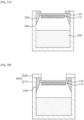
- the reaction vessel (200) is provided with a rack (250) in an upper region without a seed crystal holder, and the protective layer has a diameter larger than that of the seed crystal, whereby it covers the entire rear side of the seed crystal and has a protrusion member that protrudes outward from the periphery of the seed crystal.
- the protrusion member of the protective layer may be placed in an upper region of the reaction vessel for placing the seed crystal.
- the reaction vessel (200) is provided with a rack (250) on the upper inner wall without a seed crystal holder.
- the protrusion member of the protective layer (120) may be placed on the rack (250) for placing the seed crystal (110).
- the seed crystal (110) may be placed such that the front side of the seed crystal faces the SiC raw material (300). That is, the seed crystal may be placed such that the front side (i.e., the growing side) of the seed crystal (110) faces the bottom of the reaction vessel (200) and that the rear side (i.e., the side provided with a protective layer) faces the top of the reaction vessel.
- the shape of the rack (250) is not particularly limited as long as it has a structure on which the protrusion member of the protective layer may be placed.
- the rack (250) may have a shape in which the groove is cut from the cross-section to a "[" shape, and the protrusion member of the protective layer (120) may be fit in the groove.
- the rack (250) may have a shape of a flat top end, and the protrusion member of the protective layer may be placed on the rack.
- the upper region of the reaction vessel may be closed by a lid.
- the reaction vessel may have a structure in which its upper region is open, and the reaction vessel may be closed by a seed crystal placed in an upper region of the reaction vessel.
- the reaction vessel (200) is provided with no lid or an open-type lid (220) in an upper region.
- the reaction vessel may be closed by a seed crystal (provided with a protective layer) to be fit in the groove of the rack (250).
- the reaction vessel (200) may be a crucible and is made of a material having a melting point higher than the sublimation temperature of SiC.
- the reaction vessel may be composed of a carbonaceous component, specifically a graphite component.
- the rack may be composed of a carbonaceous component, which is the same as, or different from, that of the reaction vessel.
- the SiC raw material may be, for example, an SiC powder.
- reaction vessel may be wrapped with a heat insulation material and placed in a reaction chamber (e.g., a quartz tube or the like) having a heating means.
- a reaction chamber e.g., a quartz tube or the like
- the heating means may be, for example, an induction heating coil or resistance heating means.
- an SiC single crystal ingot is grown on the front side of the seed crystal from the SiC raw material.
- the growth of an ingot may be carried out by the growth of an SiC single crystal ingot (400) on the seed crystal (110) by sublimating the SiC raw material (300).
- the step of growing an SiC single crystal ingot may be carried out by heating under the conditions of 2,000 to 2,500°C and 1 to 200 torr, under the conditions of 2,200 to 2,400°C and 1 to 150 torr, under the conditions of 2,200 to 2,300°C and 1 to 100 torr, or under the conditions of 2,250 to 2,300°C and 1 to 50 torr.
- the temperature and pressure conditions for the growth of an SiC single crystal ingot may be employed without any particular limitation, provided that the growth is carried out under a reduced pressure condition as compared with the temperature and pressure conditions under which the SiC raw material is sublimated.
- the temperature and pressure conditions exemplified in the above as specific numerical ranges may be adjusted to an appropriately higher pressure condition if the growth is carried out under a higher temperature condition, thereby producing the same effect.
- the seed crystal Upon the heating for the growth as described above, the seed crystal is also heated. According to the invention, a protective layer is formed on the rear side of the seed crystal. Thus, it is possible to prevent loss of the rear side of the seed crystal that may otherwise occur during the heating.
- a filler may be contained in the carbonaceous protective layer to prevent cracks or the like that may be generated in the protective layer during the thermal treatment.
- the carbonaceous protective layer may be formed in multiple layers, which have different physical properties from each layer, whereby the layer quality, the adhesion between the seed crystal and the protective layer, and the thickness of the protective layer may be improved as compared with the case where the protective layer is formed in a single layer.
- the layer quality, the adhesion between the seed crystal and the protective layer, and the thickness of the protective layer may be improved as compared with the case where the protective layer is formed in a single layer.
- the protective layer has a diameter larger than that of the seed crystal, whereby it has a protrusion member that protrudes outward. Since the protrusion member is used as a support (since the seed crystal has no rack), it is possible to obtain an ingot having a large diameter by preventing the diameter thereof from being reduced during the growth of an SiC single crystal ingot while producing an effect similar to the case where a seed crystal holder is used, even though the conventional method in which a seed crystal is attached to a seed crystal holder is not adopted. Since the seed crystal is not in direct contact with the reaction vessel, which is a heating body, the loss and contamination of the seed crystal can be suppressed.
- an SiC single crystal ingot can be prepared with a large diameter.
- an SiC single crystal ingot upon the growth step according to the embodiment may have a diameter of 2 inches or more, 3 inches or more, 4 inches or more, 5 inches or more, or even 6 inches or more.
- an SiC single crystal ingot prepared according to the embodiment may have a diameter ranging from 2 to 10 inches, from 2 to 8 inches, from 4 to 8 inches, or from 4 to 6 inches.
- an SiC single crystal ingot can be grown with high quality.
- an SiC single crystal ingot may have a purity of 99% or more, 99.5% or more, or even 99.9% or more.
- Example A The materials used in Example A below are as follows:
- Example A1-1 Preparation of a seed crystal provided with a protective layer
- the liquid phenolic resin was mixed with crystalline flake graphite as a filler in a weight ratio of 7:3.
- the mixture was further mixed with additives such as a wetting dispersant and a defoaming agent in an amount of 3 parts by weight or less per 100 parts by weight of the mixture, which was dispersed to obtain a composition.
- the composition was spin-coated on one side of the silicon carbide seed crystal to obtain a coating layer having a thickness of 0.5 mm.
- the seed crystal thus coated was placed in a heater, heated at a rate of 1°C/min to reach 600°C, and then thermally treated for 2 hours to carbonize the coating layer. Thereafter, it was cooled at a rate of 1°C/min to obtain a seed crystal provided with a carbonaceous protective layer on one side.
- Example A1-2 Preparation of a seed crystal provided with a protective layer
- the liquid phenolic resin was mixed with crystalline flake graphite as a filler in a weight ratio of 95:5.
- the mixture was further mixed with additives such as a wetting dispersant and a defoaming agent in an amount of 3 parts by weight or less per 100 parts by weight of the mixture, which was dispersed to obtain a composition.
- the composition was spin-coated on one side of the silicon carbide seed crystal to obtain a coating layer having a thickness of 0.5 mm.
- the seed crystal thus coated was placed in a heater, heated at a rate of 1°C/min to reach 600°C, and then thermally treated for 2 hours to carbonize the coating layer. Thereafter, it was cooled at a rate of 1°C/min to obtain a seed crystal provided with a carbonaceous protective layer on one side.
- Example A1-3 Preparation of a seed crystal provided with a protective layer
- the liquid phenolic resin was mixed with crystalline flake graphite as a filler in a weight ratio of 5:95.
- the mixture was further mixed with additives such as a wetting dispersant and a defoaming agent in an amount of 3 parts by weight or less per 100 parts by weight of the mixture, which was dispersed to obtain a composition.
- the composition was spin-coated on one side of the silicon carbide seed crystal to obtain a coating layer having a thickness of 0.5 mm.
- the seed crystal thus coated was placed in a heater, heated at a rate of 1°C/min to reach 600°C, and then thermally treated for 2 hours to carbonize the coating layer. Thereafter, it was cooled at a rate of 1°C/min to obtain a seed crystal provided with a carbonaceous protective layer on one side.
- Example A1-4 Preparation of a seed crystal provided with a protective layer
- a polyacrylonitrile (PAN) resin, DMSO as a solvent, and crystalline flake graphite as a filler were mixed at a weight ratio of 3:5:2 and dispersed to obtain a composition.
- the composition was spin-coated on one side of the silicon carbide seed crystal to obtain a coating layer having a thickness of 0.5 mm.
- the seed crystal thus coated was placed in a heater, heated at a rate of 0.5°C/min to reach 600°C, and then thermally treated for 2 hours to carbonize the coating layer. Thereafter, it was cooled at a rate of 1°C/min to obtain a seed crystal provided with a carbonaceous protective layer on one side.
- Example A1-5 Preparation of a seed crystal provided with a protective layer
- a polyacrylonitrile (PAN) resin, DMSO as a solvent, and crystalline flake graphite as a filler were mixed at a weight ratio of 3:5:2 and dispersed to obtain a composition.
- the composition was spin-coated on one side of the silicon carbide seed crystal to obtain a coating layer having a thickness of 0.5 mm.
- the seed crystal thus coated was placed in a heater, heated at a rate of 1°C/min to reach 2,200°C, and then thermally treated for 2 hours to graphitize the coating layer. Thereafter, it was cooled at a rate of 1°C/min to obtain a seed crystal provided with a graphitized carbonaceous protective layer on one side.
- Comparative Example A1 Preparation of a seed crystal provided with a protective layer (without a filler)
- the liquid phenolic resin without being mixed with the filler, was spin-coated on one side of the silicon carbide seed crystal to obtain a coating layer having a thickness of 0.4 mm.
- the seed crystal thus coated was placed in a heater, heated at a rate of 1°C/min to reach 600°C, and then thermally treated for 2 hours to carbonize the coating layer. Thereafter, it was cooled at a rate of 1°C/min, and the coating layer was observed. As a result, it was confirmed that the coating layer was cracked due to shrinkage thereof and that the coating was peeled off.
- a graphite crucible provided with a rack on the upper inner wall was prepared.
- An SiC powder (purity: about 98%) was charged as a raw material to the lower region of the crucible.
- the seed crystal provided with a protective layer on one side as prepared in the above Example A1-1 was placed on the rack in the crucible. In such event, the seed crystal was merely placed on the rack without adhesion thereto.
- the protective layer faced the top of the crucible, and the side without the protective layer faced the bottom of the crucible.
- the crucible was wrapped with a heat insulation material and placed in a reaction chamber provided with a heating coil. After the inside of the crucible was made to be a vacuum, argon gas was gradually injected to reach the atmospheric pressure, and the pressure was then gradually reduced. In addition, the temperature in the crucible was increased to 2,300°C. Thereafter, an SiC single crystal ingot was grown on the side of the seed crystal without the protective layer for 100 hours at 2,300°C and 20 torr. As a result, an SiC single crystal ingot having a diameter of 4 inches was obtained.
- Test Example A1 Evaluation of the surface of a protective layer
- the surface of the protective layer was observed with the naked eyes or an optical microscope. As a result, the surface of the protective layer prepared in the Examples was overall excellent.
- the coating of the protective layer in Example A1-1 was the most excellent without shrinkage or peeling-off.
- Comparative Example A1 the coating layer was cracked due to shrinkage thereof, and the coating was peeled off.
- Test Example A2 Evaluation of cracks on the surface of a single crystal ingot
- Example A2 For the SiC single crystal ingot obtained in Example A2, the surface of the ingot was observed with the naked eyes or an optical microscope. As a result, no cracks were found on the surface of the ingot.
- Example B Preparation and use of a seed crystal provided with a multilayered protective layer
- Example B The materials used in Example B below are as follows:
- Example B1 Preparation of a seed crystal provided with a protective layer (multilayered and a filler contained)
- Step (1) Preparation of a coating composition
- the binder resin was mixed with the solvent to prepare a solution having a solids content of about 10% by weight, to which about 135 parts by weight of the filler was added per 100 parts by weight of the binder resin.
- the mixture was further mixed with additives such as a wetting dispersant and a defoaming agent in an amount of 5 parts by weight or less, which was dispersed to obtain a first composition.
- the binder resin was mixed with the solvent to prepare a solution having a solids content of about 13% by weight, to which about 90 parts by weight of the filler was added per 100 parts by weight of the binder resin.
- the mixture was further mixed with additives such as a wetting dispersant and a defoaming agent in an amount of 5 parts by weight or less, which was dispersed to obtain a second composition.
- Step (2) Formation of a first carbonaceous layer
- the first composition was spin-coated on the rear side (i.e., the opposite side to the growing side) of the silicon carbide seed crystal to obtain a first coating layer having a thickness of 5 ⁇ m.
- the seed crystal thus coated was placed in an oven, heated at a rate of 1°C/min to reach 600°C, and then thermally treated for 2 hours to carbonize the first coating layer. Thereafter, it was cooled at a rate of 1°C/min to obtain a seed crystal provided with a first carbonaceous layer formed on the rear side.
- Step (3) Formation of a second carbonaceous layer
- the second composition was spin-coated on the surface of the first carbonaceous layer to obtain a second coating layer having a thickness of 20 ⁇ m.
- the seed crystal thus coated was placed in an oven, heated at a rate of 1°C/min to reach 600°C, and then thermally treated for 2 hours to carbonize the second coating layer. Thereafter, it was cooled at a rate of 1°C/min to obtain a seed crystal provided with a first carbonaceous layer and a second a first carbonaceous layer sequentially formed on the rear side.
- Step (4) Formation of an additional carbonaceous layer
- the second composition was spin-coated on the surface of the second carbonaceous layer and then thermally treated to form an additional carbonaceous layer.
- Comparative Example A1 Preparation of a seed crystal provided with a protective layer (single-layered and a filler not contained)
- the liquid phenolic resin without being mixed with the filler, was spin-coated on one side of the silicon carbide seed crystal to obtain a coating layer having a thickness of 400 ⁇ m.
- the seed crystal thus coated was placed in a heater, heated at a rate of 1°C/min to reach 600°C, and then thermally treated for 2 hours to carbonize the coating layer. Thereafter, it was cooled at a rate of 1°C/min to obtain a seed crystal provided with a single-layered carbonaceous protective layer formed on the rear side.
- Example B2 Growth of a silicon carbide single crystal ingot
- a graphite crucible provided with a rack on the upper inner wall was prepared.
- the SiC powder was charged as a raw material to the lower region of the crucible.
- the seed crystal provided with a protective layer as prepared in the above Example B1 was placed on the rack in the crucible. In such event, the seed crystal was merely placed on the rack without adhesion thereto.
- the rear side i.e., the side provided with a protective layer
- the front side i.e., the side without a protective layer
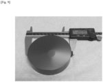
- the crucible was closed with a lid, wrapped with a heat insulation material, and placed in a reaction chamber provided with a heating coil. After the inside of the crucible was made to be a vacuum, argon gas was gradually injected to reach the atmospheric pressure, and the pressure was then gradually reduced. In addition, the temperature in the crucible was increased to 2,300°C. Thereafter, an SiC single crystal ingot was grown on the side of the seed crystal without the protective layer for 100 hours at 2,300°C and 20 torr. As a result, an SiC single crystal ingot having a diameter of 4 to 6 inches was obtained as shown in Fig. 9 .
- Test Example B1 Evaluation of the physical properties of a protective layer
- the protective layer was measured using a thermal diffusivity measurement device (LFA447, NETZCH) to have a thermal diffusivity of 143 mm 2 /s.
- the protective layer was measured to have a thermal conductivity of 158.5 W/mK, a density of 1.3 g/cm 3 , and a specific heat of 0.85 J/gK.
- Test Example B2 Observation of the cross-section of a protective layer
- Figs. 8A to 8C the left-hand side shows the seed crystal, and the right-hand side shows the protective layer.
- Test Example B3 Evaluation of the surface of a protective layer
- Example B1 the surface of the protective layer provided on the seed crystal prepared in Example B1 was observed upon the growth of a single crystal ingot. Further, a single crystal ingot was grown according to the procedure of Example B2 using the seed crystal provided with a protective layer prepared in Comparative Example B1, and the surface of the protective layer was then observed.
- Fig. 7A(a) is a photograph of the protective layer provided on the seed crystal prepared in Example B1.
- Fig. 7A(b) is a photograph of the surface of the protective layer upon the growth of a single crystal ingot using the same.
- Fig. 7B(a) is a photograph of the protective layer provided on the seed crystal prepared in Comparative Example B1.
- Fig. 7B(b) is a photograph of the surface of the protective layer upon the growth of a single crystal ingot using the same.
- the protective layer prepared in Example B1 had an excellent surface without peeling-off or cracks.
- the protective layer prepared in Comparative Example B1 had a poor surface with peeling-off and cracks.
- Test Example B4 Evaluation of cracks on the surface of a single crystal ingot
- Example B2 For the SiC single crystal ingot obtained in Example B2, the surface of the ingot was observed with the naked eyes or an optical microscope. As a result, no cracks were found on the surface of the ingot.
- Example C The materials used in Example C below are as follows:
- Example C1 Preparation of a seed crystal provided with a protective layer (having a protrusion member)
- Step (1) Preparation of a coating composition
- the binder resin was mixed with the solvent to prepare a solution having a solids content of 5 to 15% by weight, to which about 90 parts by weight of the filler was added per 100 parts by weight of the binder resin.
- the mixture was further mixed with additives such as a wetting dispersant and a defoaming agent in an amount of 5 parts by weight or less, which was dispersed to obtain a composition.
- Step (2) Preparation of a protective layer
- the coating composition thus prepared was coated on both sides of the cellulose fiber substrate having a thickness of about 140 ⁇ m using a roll coating equipment to a total thickness of 2,000 ⁇ m, which was molded to a sheet form to prepare a protective film.
- a first release film and a second release film were laminated on the first and second sides of the protective layer, respectively.
- the protective layer having the release films was cut to conform to the seed crystal.
- the first release film/protective film/second release film was cut in the form of a circle having a diameter larger than that of the seed crystal to be subsequently attached by about 0.8 inch.
- the region of the second release film that had the same shape and diameter as those of the seed crystal to be attached was cut out (see Fig. 4(b) ).
- the protective layer was cut into a circle having a diameter larger than that of the seed crystal.
- the first side of the protective layer was entirely covered by the first release film, and the second surface was exposed to the outside in the region to which the seed crystal was to be attached and was covered by the second release film in the other region (see Fig. 4(c) ).
- Step (3) Attachment of a seed crystal to a protective layer
- the seed crystal was placed on the second side of the protective layer previously cut such that the rear side of the seed crystal (i.e., the opposite side of the growing side) was brought into contact with the region where the second release film had been removed. Thereafter, the seed crystal on the protective layer was pressed under the conditions of a temperature of 25°C and a pressure of 0.5 kgf/inch to laminate the protective layer and the seed crystal.
- Step (4) Curing and carbonization of a protective layer
- the first release film was removed from the protective layer laminated to the seed crystal, which was then dried and cured by thermal treatment in an oven at about 105°C for 1 hour. Thereafter, the second release film was removed from the protective layer, which was then heated at a rate of 1°C/min to reach 600°C and then thermally treated for 2 hours to carbonize it.
- the protective layer had a diameter larger than that of the seed crystal, whereby it covered the entire rear side of the seed crystal and had a protrusion member that protruded outward from the periphery of the seed crystal.
- Example C2 Growth of a silicon carbide single crystal ingot
- Step (1) Placement of a seed crystal
- a graphite crucible provided with a rack on the upper inner wall was prepared.
- the SiC powder as a raw material was charged to the lower region of the crucible.
- the seed crystal provided with a protective layer as prepared in the above Example C1 was placed on the rack in the crucible. In such event, only the protrusion member of the protective layer was placed on the rack such that the seed crystal did not come into contact with the reaction vessel or the rack (see Fig. 1A ).
- the side of the seed crystal provided with a protective layer faced the top of the reaction vessel, and the side without a protective layer faced the bottom of the reaction vessel.
- Step (2) Growth of a single crystal ingot
- the crucible was closed with a lid, wrapped with a heat insulation material, and placed in a reaction chamber provided with a heating coil. After the inside of the crucible was made to be a vacuum, argon gas was gradually injected to reach the atmospheric pressure, and the pressure was then gradually reduced. In addition, the temperature in the crucible was increased to 2,300°C. Thereafter, an SiC single crystal ingot was grown on the side of the seed crystal without the protective layer for 100 hours at 2,300°C and 20 torr. As a result, an SiC single crystal ingot having a diameter of 4 to 6 inches was obtained.
- Test Example C1 Evaluation of the shrinkage of a protective layer
- the shrinkage of the protective layer in Example C1 at the time of curing and carbonization was evaluated. As a result, the shrinkage upon curing was within about 2% in the transverse direction as compared with the initial state, and the shrinkage upon carbonization was within about 10% in the transverse direction as compared with the initial state. Thus, the shrinkage was small.
- Test Example C2 Evaluation of the surface and cross-section of a protective layer
- Example C1 The surface and cross-section of the protective layer prepared in Example C1 were observed. As a result, the protective layer prepared in Example C1 was excellent since it had no peeling-off or cracks on the surface as shown in Fig. 10A . The layered structure was clearly confirmed on the cross-section as shown in Fig. 10B . Meanwhile, in Fig. 10A , the curved shape according to the fiber structure of the substrate layer was also observed on the surface of the protective layer.
- Test Example C3 Changes in quality of a seed crystal and an ingot upon growth
- Example C2 For the seed crystal upon the growth in Example C2, the quality thereof was observed with the naked eyes or an optical microscope. As a result, no cracks were found on the surface of the ingot.
- Fig. 11A the left-hand side is a photograph of the grown ingot, and the right-hand side is a UV image thereof. As confirmed therefrom, no cracks were found on the surface of the grown ingot in Example C2.
- an ingot was grown using the conventional method shown in Fig. 6A (a seed crystal attached to a holder) as a comparative example. The quality thereof was observed with the naked eyes or an optical microscope.
- Fig. 11B the left-hand side is a photograph of the grown ingot, and the right-hand side is a UV image thereof. As confirmed therefrom, cracks (in the dotted region) caused by internal stress were found on the surface of the grown ingot in the Comparative Example.
Landscapes
- Chemical & Material Sciences (AREA)
- Engineering & Computer Science (AREA)
- Crystallography & Structural Chemistry (AREA)
- Materials Engineering (AREA)
- Metallurgy (AREA)
- Organic Chemistry (AREA)
- Inorganic Chemistry (AREA)
- Crystals, And After-Treatments Of Crystals (AREA)
Description
- The following embodiments relate to a process for preparing a seed crystal with a protective layer.
- A single crystal of silicon carbide (SiC), silicon (Si), gallium nitride (GaN), sapphire (Al2O3), gallium arsenide (GaAs), aluminum nitride (AlN), or the like has characteristics that cannot be expected from a polycrystal counterpart thereof. Thus, a demand therefor in the industries is increasing.
- In particular, single crystal silicon carbide (SiC) has a large energy band gap and is excellent in maximum break field voltage and thermal conductivity as compared with silicon (Si). In addition, the carrier mobility of single crystal silicon carbide is comparable to that of silicon, and the saturation drift rate of electrons and the breakdown voltage thereof are large as well. By virtue of such characteristics, single crystal silicon carbide is expected to be applied to semiconductor devices that require high efficiency, high breakdown voltage, and large capacity.
- As a method for preparing such a single crystal, for example,
Japanese Laid-open Patent Publication No. 2001-114599 -
US 2013/171403 A1 teaches a method for producing an SiC volume monocrystal by sublimation growth. -
CN 101 985 773 B discloses a seed crystal treatment method for silicon carbide growth and a silicon carbide mono-crystal growing method using the same. - Another seed crystal processing method for silicon carbide single crystal growth is provided in
CN 106 757 321 A . - In order to grow a single crystal ingot, a step of adhering a seed crystal is generally carried out in advance. For example, in a conventional process referring to
Fig. 6A , an adhesive (150) is applied between a seed crystal holder (190) and a seed crystal (110), which are pressed to adhere the seed crystal. Thereafter, a raw material (300) is heated and sublimated in a reaction vessel (200), whereby a single crystal ingot is grown on the front side of the seed crystal (110). - In the conventional process in which a seed crystal is adhered to a holder located in an upper region of a reaction vessel, a difference in the coefficient of thermal expansion (CTE) between the seed crystal and the holder causes a warp (see
Fig. 6B ) or cracks due to the residual stress in the heating process. This phenomenon is further aggravated as the diameter of the single crystal ingot becomes larger as it grows, which makes it difficult to grow a single crystal ingot having a large diameter. - In addition, in the conventional process in which a seed crystal is adhered to a holder located in an upper region of a reaction vessel with an adhesive, there have been problems such as deterioration in quality during the growth of the single crystal ingot due to the adhesive, detachment of the seed crystal, contamination of the surface of the seed crystal, and the like.
- Disclosed herein, but not claimed, is a process for growing a single crystal ingot without adhesion of a seed crystal to a holder, thereby growing an SiC single crystal ingot having a large diameter and high quality.
- The present invention provides a process for preparing a seed crystal provided with a protective layer for use in the above process.
- There is provided a process for preparing a seed crystal provided with a protective layer, which comprises molding a composition that comprises a binder resin into a sheet form to prepare a protective layer;
- cutting the protective layer and attaching it to the rear side of a seed crystal of a silicon carbide (SiC) single crystal by pressure thereon; and
- curing and carbonizing the protective layer attached to the seed crystal,
- wherein the protective layer has a diameter larger than that of the seed crystal, whereby it covers the entire rear side of the seed crystal and has a protrusion member that protrudes outward from the periphery of the seed crystal.
- As disclosed herein, an SiC single crystal ingot is grown without attaching a seed crystal to a holder. Since no warp or cracks due to the residual stress caused by a difference in the thermal expansion coefficient between the single crystal ingot and the holder would be generated in the heating process, it is possible to grow a single crystal ingot having a large diameter.
- In addition, according to this aspect of the disclosure, it is not necessary to apply an adhesive to a seed crystal. Thus, it is possible to prevent deterioration in quality caused by the adhesive.
- According to the invention, a cured and carbonaceous protective layer is formed on the rear side of a seed crystal of a silicon carbide single crystal. The protective layer has a protrusion member that protrudes outward from the periphery of the seed crystal. Thus, it is possible to prevent loss of the rear side of the seed crystal that may otherwise occur during the heating for the growth thereof.
-
-
Figs. 1A ,2A, and 2B show the configurations of a reaction vessel for preparing a SiC single crystal ingot, which do not form part of the present invention. -
Fig. 1B shows a method of growing an SiC single crystal ingot, which does not form part of the present invention. -
Figs. 3A and 3B show a cross-section of a seed crystal provided with a protective layer according to a specific embodiment. -
Fig. 4 shows a method of forming a protective layer, which does not form part of the present invention. -
Fig. 5 shows a method of attaching a protective layer to a seed crystal according to another specific embodiment. -
Fig. 6A shows the configuration of a reaction vessel for preparing a SiC single crystal ingot according to a conventional process. -
Fig. 6B shows warp due to a difference in the coefficient of thermal expansion between a seed crystal holder and a seed crystal. -
Figs. 7A and 7B are each a photograph of the surface of a protective layer provided on the seed crystals prepared in Example B1 and Comparative Example B1, which do not form part of the present invention. -
Figs. 8A to 8C are microscopic images of the first carbonaceous layer, the second carbonaceous layer, and the third carbonaceous layer, respectively, observed on a cross-section of the seed crystal provided with a protective layer prepared in Example B1, which does not form part of the present invention. -
Fig. 9 is a photograph of the SiC single crystal ingot prepared in Example B2, which does not form part of the present invention. -
Figs. 10A and 10B are microscopic images showing the surface and the cross-section of a protective layer prepared in Example C1, respectively. -
Figs. 11A and 11B are photographs of the SiC single crystal ingots prepared in Example C2 and the Comparative Example, respectively. - Hereinafter, the embodiments will be described in detail with reference to the accompanying drawings. In the following detailed description, the positions referred to as upper or lower are to be understood with reference to the drawings. The drawings referred to in the following description may be exaggerated in size, spacing, and the like for the sake of description. In addition, what is obvious to a person of ordinary skill in the art may be omitted in the following description.
- The process for preparing a seed crystal provided with a protective layer comprises molding a composition that comprises a binder resin into a sheet form to prepare a protective layer;
- cutting the protective layer and attaching it to the rear side of a seed crystal of a silicon carbide (SiC) single crystal by pressure thereon; and
- curing and carbonizing the protective layer attached to the seed crystal,
- wherein the protective layer has a diameter larger than that of the seed crystal, whereby it covers the entire rear side of the seed crystal and has a protrusion member that protrudes outward from the periphery of the seed crystal.
- This specific embodiment does not form part of the present invention. The process for preparing a seed crystal provided with a protective layer comprises (a1) preparing a composition that comprises a binder resin and a filler; and (a2) coating the composition on the rear side of a seed crystal of an SiC single crystal and thermally treating the coated composition to form a carbonaceous protective layer, wherein the carbonaceous protective layer has a thickness of 5 to 1,000 µm, and the filler is a carbon-based filler, a metal-based filler, or a composite filler thereof.
- The filler added in the preparation of a carbonaceous protective layer prevents cracks or the like that may be generated in the protective layer during the thermal treatment.
- Each step will be described in detail below.
- In the above step (a1), a composition that comprises a binder resin and a filler is prepared.
- The binder resin is the main component of a coating layer for the preparation of a protective layer. The binder resin may be, for example, a phenolic resin, a polyacrylonitrile resin, a pitch-based resin, a polyvinyl chloride resin, a polyacrylic acid resin, a furan-based resin, an epoxy-based resin, or a mixed resin thereof.
- It is preferable that the binder resin has a high actual carbon ratio. For example, the binder resin may have an actual carbon ratio of 5 to 50% or 10 to 30% in an inert gas atmosphere.
- In addition, the binder resin is preferably a curable resin. For example, it may be a thermosetting resin.
- The filler serves to promote carbonization or graphitization during the thermal treatment after the formation of a coating layer and to prevent cracks from being generated due to an excessive shrinkage.
- The filler may be, for example, a carbon-based filler, a metal-based filler, or a composite filler thereof. Specifically, the filler may comprise a component such as flake graphite, amorphous graphite, expanded graphite, carbon black, carbon nanotubes, graphene, tantalum (Ta), tungsten (W), rhenium (Re), molybdenum (Mo), hafnium (Hf), tantalum carbide (TaC), tungsten carbide (WC), and the like.
- The filler may be employed in an amount of 5 to 95% by weight, 5 to 60% by weight, 10 to 50% by weight, or 20 to 40% by weight, based on the total weight of the composition. As another example, the filler may be employed in the composition in an amount of 10 to 200 parts by weight or 30 to 150 parts by weight per 100 parts by weight of the binder resin. If the content of the filler is within the above preferable ranges, it may be more advantageous in preventing shrinkage and cracks, which may be generated during the thermal treatment after the formation of a coating layer, to thereby form a protective layer having an excellent surface.
- The composition is preferably a liquid composition for the efficiency of coating.
- Thus, the composition may comprise a solvent such as ethanol, methanol, acetone, dimethylformamide (DMF), dimethylsulfoxide (DMSO), and the like. In such event, the solids content of the liquid composition may be 10 to 90% by weight or 20 to 50% by weight.
- The composition may further comprise a wetting dispersant, a defoaming agent, or the like.
- In the above step (a2), the composition prepared in the previous step is coated on the rear side of a seed crystal of an SiC single crystal, which is then thermally treated to form a carbonaceous protective layer.
- The composition is coated on the rear side (112) of a seed crystal (110) of an SiC single crystal to obtain a coating layer (120'), which is then carbonized or graphitized by thermal treatment to form a carbonaceous protective layer (120).
- In this specification, the "front side" of a seed crystal refers to one of the two sides of the seed crystal generally having a wide and flat shape on which a single crystal ingot grows. On the other hand, the "rear side" of a seed crystal refers to the opposite side of the seed crystal to the side on which a single crystal ingot grows.
- In a conventional process, an adhesive is applied to the rear side of a seed crystal, which is then attached to a holder. According to the embodiment, however, a protective layer is formed on the rear side of a seed crystal, which is not attached to a holder.
- As the seed crystal, any seed crystal having various crystal structures such as 4H-SiC, 6H-SiC, 3C-SiC, and 15R-SiC may be used depending on the kind of crystals to be grown.
- The seed crystal may be subjected to cleaning prior to the coating. A silicon dioxide layer may be formed on the surface of a seed crystal by a reaction of silicon with oxygen. It is preferable that such an oxide layer is removed in advance by cleaning since it may have the seed crystal detached or may cause defects when a single crystal ingot is grown in the subsequent process. The cleaning may be carried out with acetone, alcohol, distilled water, an acid solution, or the like, and may be carried out by ultrasonic treatment or immersion. It may be performed once, twice, or more.
- Thereafter, the coating is carried out on the rear side of the seed crystal.
- A conventional coating method such as spin coating and tape casting may be used for the coating.
- In addition, the coating may be carried out in a thickness range of 10 to 2,000 µm or in a thickness range of 20 to 1,500 µm. If the coating thickness is too smaller than the above preferable range, there is a possibility that the protective layer upon the thermal treatment may not serve as a protective layer. On the other hand, if it is too large, bubbles or cracks may be generated, or the coating layer may be peeled off, upon the thermal treatment.
- Thereafter, the coating layer is dried and cured at a temperature of 30 to 300°C or at a temperature of 50 to 200°C, followed by thermal treatment at a temperature of 300°C or higher, for example, 300 to 2,200°C to form a carbonaceous protective layer through carbonization thereof.
- The binder resin contained in the composition is carbonized or graphitized by the thermal treatment to form a carbonaceous protective layer. In addition, the filler in the coating layer may prevent cracks that may be generated during the thermal treatment and promote the carbonization or graphitization.
- The temperature of thermal treatment may be 400°C or higher, 500°C or higher, or 600°C or higher, for example, 400 to 1,500°C, 500 to 1,000°C, 1,500 to 2,500°C, or 2,000 to 2,500°C. In addition, the thermal treatment may be carried out for 1 to 10 hours or 1 to 5 hours.
- In an embodiment, the thermal treatment may be carried out under the conditions of a temperature elevation rate of 0.5 to 5°C/min and a temperature of 500°C or higher or 600°C or higher. For example, it may be carried out by raising the temperature to 500 to 1000°C, maintaining the temperature for 1 to 5 hours for heating, and then lowering the temperature at a rate of 0.5 to 5°C/min.
- In another embodiment, the thermal treatment may be carried out under the conditions of a temperature elevation rate of 1 to 5°C/min and a temperature of 1,500°C or higher or 2,000°C or higher. For example, it may be carried out by raising the temperature to 1,500 to 2,500°C or 2,000 to 2,500°C, maintaining the temperature for 1 to 5 hours for heating, and then lowering the temperature at a rate of 1 to 5°C/min.
- The thermal treatment may be carried out in an inert gas atmosphere. For example, it may be carried out in an argon gas or nitrogen gas atmosphere.
- The thermal treatment may be carried out by induction heating or by resistance heating. That is, the thermal treatment may be carried out in an induction heating furnace or in a resistance heating furnace.
- The process for preparing a seed crystal provided with a protective layer according to the present invention comprises (c1) molding a composition that comprises a binder resin into a sheet form to prepare a protective layer; (c2) cutting the protective layer and attaching it to the rear side of a seed crystal of a silicon carbide (SiC) single crystal by pressure thereon; and (c3) curing and carbonizing the protective layer attached to the seed crystal, wherein the protective layer has a diameter larger than that of the seed crystal, whereby it covers the entire rear side of the seed crystal and has a protrusion member that protrudes outward from the periphery of the seed crystal.
- A carbonaceous protective layer is formed on the rear side of a seed crystal. Thus, it is possible to prevent loss of the rear side of the seed crystal that may otherwise occur during the heating for the growth thereof. In particular, according to the embodiment, the protective layer in a sheet form is prepared in advance and then attached to the seed crystal, rather than it is directly formed on the surface of the seed crystal. Thus, it is possible to readily form a protective layer and to achieve a uniform thickness and layer quality.
- In particular, this process can prepare a protective layer that has a diameter larger than that of a seed crystal. As a result, the protrusion member of the protective layer is used as a support for a seed crystal when it is placed in a reaction vessel. Thus, it is possible to obtain an ingot having a large diameter by preventing the diameter thereof from being reduced during the growth of an SiC single crystal ingot while producing an effect similar to the case where a seed crystal holder is used, even though the conventional method in which a seed crystal is attached to a seed crystal holder is not adopted. In addition, since the seed crystal does not need to be in direct contact with the reaction vessel, which is a heating body, the loss and contamination of the seed crystal can be suppressed.
-
Fig. 4 shows a method of forming a protective layer on a seed crystal according to the embodiment.Fig. 5 shows a method of attaching a protective layer to a seed crystal according to still the embodiment. - Each step will be described in detail below with reference to the drawings.
- In the above step (c1), a composition that comprises a binder resin is molded into a sheet form to prepare a protective layer.
- The binder resin is the main component of a coating composition for the preparation of a protective layer. The resins as exemplified in the above embodiment may be used as the binder resin.
- The composition may further comprise a filler in addition to the binder resin. The filler serves to promote carbonization during the thermal treatment after the coating of the composition and to prevent cracks from being generated due to an excessive shrinkage. The filler may be, as exemplified in the above embodiment, a carbon-based filler, a metal-based filler, or a composite filler thereof.
- The filler may be employed in the composition in an amount of 10 to 200 parts by weight or 30 to 150 parts by weight per 100 parts by weight of the binder resin. If the content of the filler is within the above preferable range, it may be more advantageous in preventing shrinkage and cracks, which may be generated during the thermal treatment after the formation of a coating layer, to thereby form a protective layer having an excellent surface.
- As a more specific example, a phenolic resin may be used as the binder resin, graphite may be used as the filler, and the composition may comprise 50 to 120 parts by weight of the filler per 100 parts by weight of the binder resin.
- The composition may further comprise a solvent for controlling the viscosity thereof when it is molded.
- For example, the composition may comprise a solvent such as ethanol, methanol, acetone, dimethylformamide (DMF), dimethylsulfoxide (DMSO), and the like. In such event, the solids content of the composition may be 10 to 90% by weight or 20 to 50% by weight.
- The composition may further comprise a wetting dispersant, a defoaming agent, or the like.
- The composition thus prepared is molded into a sheet form to prepare a protective layer. The molding may be carried out using such a process as roll coating, comma coating, dip coating, and the like.
- The molding into a sheet form may be carried out in a thickness range of 10 to 3,000 µm or in a thickness range of 100 to 1,000 µm. If the molding thickness is too smaller than the above preferable range, there is a possibility that the tensile strength of the protective layer may be low and that the protective layer upon the thermal treatment may not serve as a protective layer. On the other hand, if it is too large, bubbles or cracks may be generated, or the coating layer may be peeled off, upon the thermal treatment.
- In addition, it is preferable to carry out a step of laminating a release film on both sides of the protective layer molded from the composition into a sheet form.
- The release film serves to prevent the problem that the surface of the protective layer is contaminated during the molding process or that the composition, which is not dried yet, comes into contact with the equipment thereby impairing the processability.
- As a preferred example, the preparation of the protective layer is carried out using roll coating. In such event, a release film is laminated on both sides of the protective layer, which release film may be removed before a subsequent curing or carbonization step.
- The release film may be a conventional release film. For example, it may be a PET film coated with silicone, a paper film coated with silicon, or the like. The release film may have a thickness of 25 to 100 µm. In addition, the release film may have a peel strength of 3 to 30 gf/inch.
- The molding of the protective layer may be carried out as a single layer or a multilayer.
- In the case of single-layer molding, the above composition only may be molded into a sheet form to prepare a protective layer.
- In the case of multi-layer molding, the composition may be coated on a core layer (i.e., a separate substrate), which is then molded into a sheet form to prepare a protective layer.
- According to a preferred example, the composition may be coated on both sides of a core layer composed of a fibrous material, which is then molded into a sheet form to prepare a protective layer.
- As a core layer of a fibrous material is used as described above, it is possible to readily form a thick protective layer, and it is more advantages in achieving a uniform thickness and layer quality. In addition, as a core layer of a fibrous material is used, the strength of the protective layer is increased to prevent the seed crystal from vanishing or peeling off when a single crystal ingot is grown, and it may be more effective to prevent deformation of the seed crystal by suppressing shrinkage of the protective layer.
- In such event, the core layer of a fibrous material may, more specifically, comprise cellulose, rayon, carbon fiber, or the like.
- More preferably, the core layer may be composed of a cellulose fiber.
- The core layer may increase the tensile strength of the protective layer, thereby improving the supporting force thereof when a seed crystal is placed in a reaction vessel for the growth of an SiC ingot.
- According to a specific example, referring to
Fig. 4(a) , the preparation of a protective layer is carried out using roll coating. In such event, the composition (123) is coated on both sides of a core layer (130) composed of a fibrous material, which is then molded into a sheet form to prepare a protective layer (120). In addition, a first release film (141) and a second release film (142) are laminated on both sides of the protective layer (120). The first release film (141) and the second release film (142) may be removed before a subsequent curing or carbonization step. - In the above step (c2), the protective layer is cut and attached to the rear side of a seed crystal of an SiC single crystal by pressure thereon.
- Since the protective layer prepared above is in a sheet form without a particular shape, it needs to be cut to be attached to the rear side of a seed crystal.
- Specifically, since the shape of the rear side of a seed crystal is generally circular, the protective layer may be cut into a circular shape.
- The protective layer is cut such that it covers the entire rear side of a seed crystal and has a protrusion member that protrudes outward from the periphery of the seed crystal.
- For example, the protective layer may be cut into a circular shape having a diameter larger than the diameter of the rear side of a seed crystal by 0.1 to 4 inches or 0.3 to 1 inch.
- Thereafter, the protective layer thus cut is attached to the rear side of a seed crystal of an SiC single crystal.
- A seed crystal that has a crystal structure exemplified in the above embodiment may be used as the seed crystal. The seed crystal may be subjected to cleaning prior to the coating.
- In addition, in order for the protective layer to be in direct contact with the rear side of the seed crystal, the release film in the region to which the seed crystal is to be attached may be removed in advance, and the protective layer is attached thereto by pressure thereon.
- Specifically, the protective layer cut into a sheet form has a structure in which a first release film is laminated on one side and a second release film is laminated on the other side. As shown in
Fig. 4(b) , the protective layer in a laminated structure as described above may be first cut into a circular shape (c2) having a diameter larger than that of the rear side of the seed crystal. Then, only the second release film (142) in the region (c1) to which the rear side of the seed crystal is to be attached may be secondarily cut out. - As a result, as shown in
Fig. 4(c) , the protective layer (120) may have a structure in which the first release film (141) is laminated on one side and the second release film (142) is laminated on the other side, and the second release film (142) in the region of to the protective layer (120) to which the seed crystal is to be attached is removed so that the protective layer (120) is exposed to the outside. In addition, the protective layer (120) may comprise a core layer (130) of a fibrous material to have an enhanced tensile strength. - Thereafter, as shown in
Figs. 5(a) and 5(b) , the rear side (112) of the seed crystal (110) of an SiC single crystal is brought into contact with the protective layer (120) thus cut, and the seed crystal is attached to the protective layer by pressure thereon (600). Preferably, since the protective layer (120) comprises an uncured binder resin, the protective layer and the seed crystal can be readily attached by pressure thereon (600). - In the above step (c3), the protective layer attached to the seed crystal is cured and carbonized.
- For example, the protective layer may be dried and cured by thermal treatment at a temperature of 30 to 300°C or at a temperature of 50 to 200°C.
- Thereafter, the protective layer thus cured may be carbonized or graphitized by thermal treatment at a temperature of 300°C or higher, for example, 300 to 2,200°C.
- The binder resin contained in the protective layer is carbonized or further graphitized by the thermal treatment to form a carbonaceous protective layer. In addition, the filler in the protective layer may prevent cracks that may be generated during the thermal treatment and promote the carbonization or graphitization.
- More specific methods and conditions of the thermal treatment may employ the specific methods and conditions exemplified in the preparation of a carbonaceous protective layer in the above embodiment.
- The carbonization is preferably carried out once all of the release films attached to the protective layer have been removed.
- As a specific example, as shown in
Fig. 5(c) , it is preferable to remove the first release film (141) provided on the side of the protective layer (120) to which the seed crystal (110) is not attached and then carry out the curing step since the solvent is readily volatilized. In such event, it is advantageous in preventing deformation of the protective layer and suppressing fusion to leave the second release film (142) provided on the side of the protective layer (120) to which the seed crystal (110) has been attached. After the curing, as shown inFig. 5(d) , the second release film (142) is removed from the protective layer (120), and the carbonization may then be carried out. - A seed crystal having a carbonized protective layer is obtained through the above steps. The total thickness of the carbonized protective layer may be 5 to 1,500 µm, 10 to 1,000 µm, 50 to 500 µm, or 50 to 2,000 µm.
- According to the above process, a protective layer in a sheet form is prepared in advance and then attached to a seed crystal, rather than it is directly formed on the surface of the seed crystal. Thus, it is possible to readily form a protective layer and to achieve a uniform thickness and layer quality. In particular, according to the process, it is possible to prepare a protective layer having a diameter larger than that of a seed crystal (which is difficult to achieve in the case where a protective layer is directly formed on the surface of a seed crystal). As a result, the protrusion member of the protective layer is used as a support for a seed crystal when it is placed in a reaction vessel. Thus, it is possible to obtain an ingot having a large diameter by preventing the diameter thereof from being reduced during the growth of an SiC single crystal ingot while producing an effect similar to the case where a seed crystal holder is used, even though the conventional method in which a seed crystal is attached to a seed crystal holder is not adopted. In addition, since the seed crystal is not in direct contact with the reaction vessel, which is a heating body, the loss and contamination of the seed crystal can be suppressed.
- In addition, the seed crystal of an SiC single crystal provided with a protective layer comprises a seed crystal of an SiC single crystal and a carbonaceous protective layer formed on the rear side of the seed crystal.
- The seed crystal provided with a protective layer which is obtained according to the method claimed herein comprises a seed crystal of a silicon carbide (SiC) single crystal and a protective layer formed on the rear side of the seed crystal, wherein the protective layer has a diameter larger than that of the seed crystal, whereby it covers the entire rear side of the seed crystal and has a protrusion member that protrudes outward from the periphery of the seed crystal.
- As described above with respect to the process, the protective layer may be formed by carbonization or graphitization of a composition that comprises a binder resin and a filler.
- Thus, the protective layer may comprise uncrystallized carbon or crystallized carbon. For example, the protective layer may comprise a carbide or a graphitized substance of the binder resin.
- In such event, the binder resin may be a phenolic resin, a polyacrylonitrile resin, a pitch-based resin, a polyvinyl chloride resin, a polyacrylic acid resin, a furan-based resin, an epoxy-based resin, or a mixed resin thereof. In addition, the filler may be a carbon-based filler, a metal-based filler, or a composite filler thereof.
- Preferably, the protective layer may be formed by carbonization or graphitization of a composition that comprises a binder resin and a filler.
- Specifically, the protective layer may be formed by carbonization or graphitization of a composition that comprises a filler in an amount of 50 to 120 parts by weight per 100 parts by weight of the binder resin. If the content of the filler in the protective layer is within the above preferable range, it may be more advantageous in preventing cracks and detachment of the seed crystal during the growth of an ingot at high temperatures.
-
Figs. 3A and 3B show a cross-section of a seed crystal provided with a protective layer according to the embodiment. - Referring to
Fig. 3A , the seed crystal (10) provided with a protective layer comprises a seed crystal (110) of an SiC single crystal and a protective layer (120) formed on the rear side (111) of the seed crystal (110). - Alternatively, referring to
Fig. 3B , the seed crystal (10') provided with a protective layer according to another embodiment comprises a seed crystal (110) of an SiC single crystal and a protective layer (120) formed on the rear side (111) of the seed crystal (110), wherein the protective layer (120) comprises a core layer (130), which core layer (120) may be formed by carbonization of a fibrous material. - In particular, the protective layer (120) has a diameter larger than that of the seed crystal (110), whereby it covers the entire rear side (112) of the seed crystal and has a protrusion member (125) that protrudes outward from the periphery of the seed crystal.
- The protrusion member (125) may be used as a support for a seed crystal when it is placed in a reaction vessel for the growth of an SiC ingot.
- Preferably, it is advantageous for the purpose of preventing thermal shock and thermal etching of the surface of the seed crystal that the protrusion member (125) has a length in the range of 0.1 to 4 inches or in the range of 0.3 to 1 inch when viewed from a cross-section of the protective film (120).
- As a preferred example, the protective layer may have a total thickness of 50 to 2,000 µm, and the protrusion member may have a length in the range of 0.3 to 1 inch when viewed from a cross-section of the protective film. In addition, in such event, the protective layer may comprise a core layer formed by carbonization of a fibrous material.
- A process for growing a silicon carbide (SiC) single crystal ingot, which is not claimed, comprises (1) forming a protective layer on the rear side of a seed crystal of a silicon carbide single crystal; (2) charging an SiC raw material to a lower region of a reaction vessel and placing the seed crystal on an upper region of the reaction vessel without adhesion thereto; and (3) growing an SiC single crystal ingot on the front side of the seed crystal from the SiC raw material.
- Each step will be described in detail below.
- In the above step (1), a protective layer is formed on the rear side of a seed crystal of an SiC single crystal.
- The above step (1) comprises molding a composition that comprises a binder resin into a sheet form to prepare a protective layer; cutting the protective layer and attaching it to the rear side of a seed crystal of an SiC single crystal by pressure thereon; and curing and carbonizing the protective layer attached to the seed crystal. In the above step (1), the composition may be coated on both sides of a core layer composed of a fibrous material to a sheet form. The protective layer has a diameter larger than that of the seed crystal, whereby it covers the entire rear side of the seed crystal and has a protrusion member that protrudes outward from the periphery of the seed crystal. In addition, the carbonized protective layer may have a total thickness of 50 to 2,000 µm.
- In the above step (2), an SiC raw material is charged to a lower region of a reaction vessel, and the seed crystal is placed on an upper region of the reaction vessel without adhesion thereto.
- In the process, the seed crystal is not adhered to a holder as described above. The reaction vessel is not provided with a holder for the adhesion of a seed crystal.
- As an example, the reaction vessel (200) is provided with a rack (250) in an upper region without a seed crystal holder, and the protective layer has a diameter larger than that of the seed crystal, whereby it covers the entire rear side of the seed crystal and has a protrusion member that protrudes outward from the periphery of the seed crystal. The protrusion member of the protective layer may be placed in an upper region of the reaction vessel for placing the seed crystal. Specifically, referring to
Fig. 1A , the reaction vessel (200) is provided with a rack (250) on the upper inner wall without a seed crystal holder. The protrusion member of the protective layer (120) may be placed on the rack (250) for placing the seed crystal (110). In such event, the seed crystal (110) may be placed such that the front side of the seed crystal faces the SiC raw material (300). That is, the seed crystal may be placed such that the front side (i.e., the growing side) of the seed crystal (110) faces the bottom of the reaction vessel (200) and that the rear side (i.e., the side provided with a protective layer) faces the top of the reaction vessel. In such event, the shape of the rack (250) is not particularly limited as long as it has a structure on which the protrusion member of the protective layer may be placed. For example, the rack (250) may have a shape in which the groove is cut from the cross-section to a "[" shape, and the protrusion member of the protective layer (120) may be fit in the groove. Alternatively, the rack (250) may have a shape of a flat top end, and the protrusion member of the protective layer may be placed on the rack. - Once the seed crystal has been placed, the upper region of the reaction vessel may be closed by a lid.
- Alternatively, the reaction vessel may have a structure in which its upper region is open, and the reaction vessel may be closed by a seed crystal placed in an upper region of the reaction vessel. For example, as shown in
Figs. 2A and 2B , the reaction vessel (200) is provided with no lid or an open-type lid (220) in an upper region. The reaction vessel may be closed by a seed crystal (provided with a protective layer) to be fit in the groove of the rack (250). - The reaction vessel (200) may be a crucible and is made of a material having a melting point higher than the sublimation temperature of SiC. For example, the reaction vessel may be composed of a carbonaceous component, specifically a graphite component. In addition, the rack may be composed of a carbonaceous component, which is the same as, or different from, that of the reaction vessel.
- In addition, the SiC raw material may be, for example, an SiC powder.
- Thereafter, the reaction vessel may be wrapped with a heat insulation material and placed in a reaction chamber (e.g., a quartz tube or the like) having a heating means. In such event, the heating means may be, for example, an induction heating coil or resistance heating means.
- In the above step (3), an SiC single crystal ingot is grown on the front side of the seed crystal from the SiC raw material.
- Referring to
Fig. 1B , the growth of an ingot may be carried out by the growth of an SiC single crystal ingot (400) on the seed crystal (110) by sublimating the SiC raw material (300). - As to the temperature and pressure conditions for growing an SiC single crystal ingot, for example, the step of growing an SiC single crystal ingot may be carried out by heating under the conditions of 2,000 to 2,500°C and 1 to 200 torr, under the conditions of 2,200 to 2,400°C and 1 to 150 torr, under the conditions of 2,200 to 2,300°C and 1 to 100 torr, or under the conditions of 2,250 to 2,300°C and 1 to 50 torr.
- However, since the growth of an SiC single crystal ingot is based on the principle that an SiC raw material is sublimated into SiC gas at a high temperature, and the SiC gas then grows into a single crystal ingot under a reduced pressure condition, the temperature and pressure conditions for the growth of an SiC single crystal ingot may be employed without any particular limitation, provided that the growth is carried out under a reduced pressure condition as compared with the temperature and pressure conditions under which the SiC raw material is sublimated.
- That is, the temperature and pressure conditions exemplified in the above as specific numerical ranges may be adjusted to an appropriately higher pressure condition if the growth is carried out under a higher temperature condition, thereby producing the same effect.
- Upon the heating for the growth as described above, the seed crystal is also heated. According to the invention, a protective layer is formed on the rear side of the seed crystal. Thus, it is possible to prevent loss of the rear side of the seed crystal that may otherwise occur during the heating.
- In addition, a filler may be contained in the carbonaceous protective layer to prevent cracks or the like that may be generated in the protective layer during the thermal treatment.
- In addition, the carbonaceous protective layer may be formed in multiple layers, which have different physical properties from each layer, whereby the layer quality, the adhesion between the seed crystal and the protective layer, and the thickness of the protective layer may be improved as compared with the case where the protective layer is formed in a single layer. As a result, it is possible to more effectively suppress the stress that may be applied during the growth of a single crystal ingot, thereby preventing deterioration in quality such as cracking of the ingot.
- According to the invention, the protective layer has a diameter larger than that of the seed crystal, whereby it has a protrusion member that protrudes outward. Since the protrusion member is used as a support (since the seed crystal has no rack), it is possible to obtain an ingot having a large diameter by preventing the diameter thereof from being reduced during the growth of an SiC single crystal ingot while producing an effect similar to the case where a seed crystal holder is used, even though the conventional method in which a seed crystal is attached to a seed crystal holder is not adopted. Since the seed crystal is not in direct contact with the reaction vessel, which is a heating body, the loss and contamination of the seed crystal can be suppressed.
- In particular, since the seed crystal is not attached to a holder, an SiC single crystal ingot can be prepared with a large diameter. For example, an SiC single crystal ingot upon the growth step according to the embodiment may have a diameter of 2 inches or more, 3 inches or more, 4 inches or more, 5 inches or more, or even 6 inches or more. As an example, an SiC single crystal ingot prepared according to the embodiment may have a diameter ranging from 2 to 10 inches, from 2 to 8 inches, from 4 to 8 inches, or from 4 to 6 inches.
- In addition, since an adhesive is not applied to a seed crystal, an SiC single crystal ingot can be grown with high quality. For example, an SiC single crystal ingot may have a purity of 99% or more, 99.5% or more, or even 99.9% or more.
- Hereinafter, more specific examples will be described for illustrative purposes. Examples A and B do not form part of the invention.
- The materials used in Example A below are as follows:
- Liquid phenolic resin: phenolic resin/methyl alcohol/water = 58 to 62:36 to 41:0 to 4 (weight ratio), Neolite KC-4703, Kangnam Chemical Co., Ltd.
- Crystalline flake graphite: average particle size (D50) of 2.5 µm
- Silicon carbide seed crystal: single crystal substrate of 4 to 6 inches in diameter, 500 to 1,200 µm in thickness, and a crystal structure of 3C, 4H, 6H, 15R.
- The liquid phenolic resin was mixed with crystalline flake graphite as a filler in a weight ratio of 7:3. The mixture was further mixed with additives such as a wetting dispersant and a defoaming agent in an amount of 3 parts by weight or less per 100 parts by weight of the mixture, which was dispersed to obtain a composition. The composition was spin-coated on one side of the silicon carbide seed crystal to obtain a coating layer having a thickness of 0.5 mm. The seed crystal thus coated was placed in a heater, heated at a rate of 1°C/min to reach 600°C, and then thermally treated for 2 hours to carbonize the coating layer. Thereafter, it was cooled at a rate of 1°C/min to obtain a seed crystal provided with a carbonaceous protective layer on one side.
- The liquid phenolic resin was mixed with crystalline flake graphite as a filler in a weight ratio of 95:5. The mixture was further mixed with additives such as a wetting dispersant and a defoaming agent in an amount of 3 parts by weight or less per 100 parts by weight of the mixture, which was dispersed to obtain a composition. The composition was spin-coated on one side of the silicon carbide seed crystal to obtain a coating layer having a thickness of 0.5 mm. The seed crystal thus coated was placed in a heater, heated at a rate of 1°C/min to reach 600°C, and then thermally treated for 2 hours to carbonize the coating layer. Thereafter, it was cooled at a rate of 1°C/min to obtain a seed crystal provided with a carbonaceous protective layer on one side.
- The liquid phenolic resin was mixed with crystalline flake graphite as a filler in a weight ratio of 5:95. The mixture was further mixed with additives such as a wetting dispersant and a defoaming agent in an amount of 3 parts by weight or less per 100 parts by weight of the mixture, which was dispersed to obtain a composition. The composition was spin-coated on one side of the silicon carbide seed crystal to obtain a coating layer having a thickness of 0.5 mm. The seed crystal thus coated was placed in a heater, heated at a rate of 1°C/min to reach 600°C, and then thermally treated for 2 hours to carbonize the coating layer. Thereafter, it was cooled at a rate of 1°C/min to obtain a seed crystal provided with a carbonaceous protective layer on one side.
- A polyacrylonitrile (PAN) resin, DMSO as a solvent, and crystalline flake graphite as a filler were mixed at a weight ratio of 3:5:2 and dispersed to obtain a composition. The composition was spin-coated on one side of the silicon carbide seed crystal to obtain a coating layer having a thickness of 0.5 mm. The seed crystal thus coated was placed in a heater, heated at a rate of 0.5°C/min to reach 600°C, and then thermally treated for 2 hours to carbonize the coating layer. Thereafter, it was cooled at a rate of 1°C/min to obtain a seed crystal provided with a carbonaceous protective layer on one side.
- A polyacrylonitrile (PAN) resin, DMSO as a solvent, and crystalline flake graphite as a filler were mixed at a weight ratio of 3:5:2 and dispersed to obtain a composition. The composition was spin-coated on one side of the silicon carbide seed crystal to obtain a coating layer having a thickness of 0.5 mm. The seed crystal thus coated was placed in a heater, heated at a rate of 1°C/min to reach 2,200°C, and then thermally treated for 2 hours to graphitize the coating layer. Thereafter, it was cooled at a rate of 1°C/min to obtain a seed crystal provided with a graphitized carbonaceous protective layer on one side.
- The liquid phenolic resin, without being mixed with the filler, was spin-coated on one side of the silicon carbide seed crystal to obtain a coating layer having a thickness of 0.4 mm. The seed crystal thus coated was placed in a heater, heated at a rate of 1°C/min to reach 600°C, and then thermally treated for 2 hours to carbonize the coating layer. Thereafter, it was cooled at a rate of 1°C/min, and the coating layer was observed. As a result, it was confirmed that the coating layer was cracked due to shrinkage thereof and that the coating was peeled off.
- A graphite crucible provided with a rack on the upper inner wall was prepared. An SiC powder (purity: about 98%) was charged as a raw material to the lower region of the crucible. In addition, the seed crystal provided with a protective layer on one side as prepared in the above Example A1-1 was placed on the rack in the crucible. In such event, the seed crystal was merely placed on the rack without adhesion thereto. In addition, the protective layer faced the top of the crucible, and the side without the protective layer faced the bottom of the crucible.
- The crucible was wrapped with a heat insulation material and placed in a reaction chamber provided with a heating coil. After the inside of the crucible was made to be a vacuum, argon gas was gradually injected to reach the atmospheric pressure, and the pressure was then gradually reduced. In addition, the temperature in the crucible was increased to 2,300°C. Thereafter, an SiC single crystal ingot was grown on the side of the seed crystal without the protective layer for 100 hours at 2,300°C and 20 torr. As a result, an SiC single crystal ingot having a diameter of 4 inches was obtained.
- For each of the seed crystals provided with a protective layer as prepared in the above Examples and Comparative Examples, the surface of the protective layer was observed with the naked eyes or an optical microscope. As a result, the surface of the protective layer prepared in the Examples was overall excellent. In particular, among Examples A1-1 to A1-3 prepared in various contents of the filler, the coating of the protective layer in Example A1-1 was the most excellent without shrinkage or peeling-off. In contrast, in Comparative Example A1, the coating layer was cracked due to shrinkage thereof, and the coating was peeled off.
- For the SiC single crystal ingot obtained in Example A2, the surface of the ingot was observed with the naked eyes or an optical microscope. As a result, no cracks were found on the surface of the ingot.
- The materials used in Example B below are as follows:
- Binder resin: phenolic resin, KC-5536, Kangnam Chemical Co., Ltd.
- Filler: crystalline flake graphite, purity of 80 to 99%, D50 of 2.5 µm
- Solvent: ethanol, OCI Co., Ltd.
- Seed crystal of an SiC single crystal: 100 to 150 mm in diameter, a crystal structure of 4H-SiC, 350 to 1,000 µm in thickness
- Powder of an SiC raw material: purity of 99.99% or more, D50 of 100 µm
- First, the binder resin was mixed with the solvent to prepare a solution having a solids content of about 10% by weight, to which about 135 parts by weight of the filler was added per 100 parts by weight of the binder resin. The mixture was further mixed with additives such as a wetting dispersant and a defoaming agent in an amount of 5 parts by weight or less, which was dispersed to obtain a first composition.
- In addition, the binder resin was mixed with the solvent to prepare a solution having a solids content of about 13% by weight, to which about 90 parts by weight of the filler was added per 100 parts by weight of the binder resin. The mixture was further mixed with additives such as a wetting dispersant and a defoaming agent in an amount of 5 parts by weight or less, which was dispersed to obtain a second composition.
- The first composition was spin-coated on the rear side (i.e., the opposite side to the growing side) of the silicon carbide seed crystal to obtain a first coating layer having a thickness of 5 µm. The seed crystal thus coated was placed in an oven, heated at a rate of 1°C/min to reach 600°C, and then thermally treated for 2 hours to carbonize the first coating layer. Thereafter, it was cooled at a rate of 1°C/min to obtain a seed crystal provided with a first carbonaceous layer formed on the rear side.
- The second composition was spin-coated on the surface of the first carbonaceous layer to obtain a second coating layer having a thickness of 20 µm. The seed crystal thus coated was placed in an oven, heated at a rate of 1°C/min to reach 600°C, and then thermally treated for 2 hours to carbonize the second coating layer. Thereafter, it was cooled at a rate of 1°C/min to obtain a seed crystal provided with a first carbonaceous layer and a second a first carbonaceous layer sequentially formed on the rear side.
- In the same manner as in the above step (3), the second composition was spin-coated on the surface of the second carbonaceous layer and then thermally treated to form an additional carbonaceous layer.
- The liquid phenolic resin, without being mixed with the filler, was spin-coated on one side of the silicon carbide seed crystal to obtain a coating layer having a thickness of 400 µm. The seed crystal thus coated was placed in a heater, heated at a rate of 1°C/min to reach 600°C, and then thermally treated for 2 hours to carbonize the coating layer. Thereafter, it was cooled at a rate of 1°C/min to obtain a seed crystal provided with a single-layered carbonaceous protective layer formed on the rear side.
- A graphite crucible provided with a rack on the upper inner wall was prepared. The SiC powder was charged as a raw material to the lower region of the crucible. In addition, the seed crystal provided with a protective layer as prepared in the above Example B1 was placed on the rack in the crucible. In such event, the seed crystal was merely placed on the rack without adhesion thereto. In addition, the rear side (i.e., the side provided with a protective layer) faced the top of the reaction vessel, and the front side (i.e., the side without a protective layer) of the seed crystal faced the bottom of the reaction vessel.
- The crucible was closed with a lid, wrapped with a heat insulation material, and placed in a reaction chamber provided with a heating coil. After the inside of the crucible was made to be a vacuum, argon gas was gradually injected to reach the atmospheric pressure, and the pressure was then gradually reduced. In addition, the temperature in the crucible was increased to 2,300°C. Thereafter, an SiC single crystal ingot was grown on the side of the seed crystal without the protective layer for 100 hours at 2,300°C and 20 torr. As a result, an SiC single crystal ingot having a diameter of 4 to 6 inches was obtained as shown in
Fig. 9 . - The physical properties of the protective layer provided on the seed crystal prepared in Example B1 were evaluated.
- The protective layer was measured using a thermal diffusivity measurement device (LFA447, NETZCH) to have a thermal diffusivity of 143 mm2/s. In addition, the protective layer was measured to have a thermal conductivity of 158.5 W/mK, a density of 1.3 g/cm3, and a specific heat of 0.85 J/gK.
- The cross-section of the seed crystal provided with a protective layer as prepared in Example B1 was observed and shown in
Figs 8A to 8C . - In
Figs. 8A to 8C , the left-hand side shows the seed crystal, and the right-hand side shows the protective layer. - In addition, in
Figs. 8A to 8C , what is indicated by the arrows are the first carbonaceous layer, the second carbonaceous layer, and the third carbonaceous layer, respectively. - Thus, it was confirmed that a multilayered protective layer was formed on the rear side of the seed crystal in the Example.
- The surface of the protective layer provided on the seed crystals prepared in Example B1 and Comparative Example B1 was observed.
- In addition, the surface of the protective layer provided on the seed crystal prepared in Example B1 was observed upon the growth of a single crystal ingot. Further, a single crystal ingot was grown according to the procedure of Example B2 using the seed crystal provided with a protective layer prepared in Comparative Example B1, and the surface of the protective layer was then observed.
-
Fig. 7A(a) is a photograph of the protective layer provided on the seed crystal prepared in Example B1.Fig. 7A(b) is a photograph of the surface of the protective layer upon the growth of a single crystal ingot using the same. In addition,Fig. 7B(a) is a photograph of the protective layer provided on the seed crystal prepared in Comparative Example B1.Fig. 7B(b) is a photograph of the surface of the protective layer upon the growth of a single crystal ingot using the same. - As a result, as shown in
Fig. 7A(a) , the protective layer prepared in Example B1 had an excellent surface without peeling-off or cracks. In contrast, as shown inFig. 7B(a) , the protective layer prepared in Comparative Example B1 had a poor surface with peeling-off and cracks. - In addition, as shown in
Fig. 7A(b) , neither holes nor vanishment was observed in the protective layer even after the growth of a single crystal ingot. In contrast, as shown inFig. 7B(b) , the protective layer prepared in the Comparative Example had holes and was observed to have vanishment. - For the SiC single crystal ingot obtained in Example B2, the surface of the ingot was observed with the naked eyes or an optical microscope. As a result, no cracks were found on the surface of the ingot.
- The materials used in Example C below are as follows:
- Binder resin: phenolic resin, KC-5536, Kangnam Chemical Co., Ltd.
- Filler: crystalline flake graphite, purity of 80 to 99%, D50 of 2.5 µm
- Solvent: ethanol, OCI Co., Ltd.
- Cellulose substrate: a cotton fabric having a thickness of 60 to 100 m/g, plain-weaved, about 140 µm in thickness
- Release film: a PET film coated with silicone, 25 to 100 µm in thickness
- Seed crystal of an SiC single crystal: 100 to 150 mm in diameter, a crystal structure of 4H-SiC, 350 to 1,000 µm in thickness
- Powder of an SiC raw material: purity of 99.99% or more, D50 of 100 µm
- The binder resin was mixed with the solvent to prepare a solution having a solids content of 5 to 15% by weight, to which about 90 parts by weight of the filler was added per 100 parts by weight of the binder resin. The mixture was further mixed with additives such as a wetting dispersant and a defoaming agent in an amount of 5 parts by weight or less, which was dispersed to obtain a composition.
- The coating composition thus prepared was coated on both sides of the cellulose fiber substrate having a thickness of about 140 µm using a roll coating equipment to a total thickness of 2,000 µm, which was molded to a sheet form to prepare a protective film. In addition, upon the molding, a first release film and a second release film were laminated on the first and second sides of the protective layer, respectively.
- Thereafter, the protective layer having the release films was cut to conform to the seed crystal.
- First, the first release film/protective film/second release film was cut in the form of a circle having a diameter larger than that of the seed crystal to be subsequently attached by about 0.8 inch. Second, the region of the second release film that had the same shape and diameter as those of the seed crystal to be attached was cut out (see
Fig. 4(b) ). - As a result, the protective layer was cut into a circle having a diameter larger than that of the seed crystal. In such event, the first side of the protective layer was entirely covered by the first release film, and the second surface was exposed to the outside in the region to which the seed crystal was to be attached and was covered by the second release film in the other region (see
Fig. 4(c) ). - The seed crystal was placed on the second side of the protective layer previously cut such that the rear side of the seed crystal (i.e., the opposite side of the growing side) was brought into contact with the region where the second release film had been removed. Thereafter, the seed crystal on the protective layer was pressed under the conditions of a temperature of 25°C and a pressure of 0.5 kgf/inch to laminate the protective layer and the seed crystal.
- The first release film was removed from the protective layer laminated to the seed crystal, which was then dried and cured by thermal treatment in an oven at about 105°C for 1 hour. Thereafter, the second release film was removed from the protective layer, which was then heated at a rate of 1°C/min to reach 600°C and then thermally treated for 2 hours to carbonize it.
- As a result, a seed crystal provided with a carbonaceous protective layer on the rear side was obtained. In such event, the protective layer had a diameter larger than that of the seed crystal, whereby it covered the entire rear side of the seed crystal and had a protrusion member that protruded outward from the periphery of the seed crystal.
- A graphite crucible provided with a rack on the upper inner wall was prepared. The SiC powder as a raw material was charged to the lower region of the crucible. In addition, the seed crystal provided with a protective layer as prepared in the above Example C1 was placed on the rack in the crucible. In such event, only the protrusion member of the protective layer was placed on the rack such that the seed crystal did not come into contact with the reaction vessel or the rack (see
Fig. 1A ). In addition, the side of the seed crystal provided with a protective layer faced the top of the reaction vessel, and the side without a protective layer faced the bottom of the reaction vessel. - The crucible was closed with a lid, wrapped with a heat insulation material, and placed in a reaction chamber provided with a heating coil. After the inside of the crucible was made to be a vacuum, argon gas was gradually injected to reach the atmospheric pressure, and the pressure was then gradually reduced. In addition, the temperature in the crucible was increased to 2,300°C. Thereafter, an SiC single crystal ingot was grown on the side of the seed crystal without the protective layer for 100 hours at 2,300°C and 20 torr. As a result, an SiC single crystal ingot having a diameter of 4 to 6 inches was obtained.
- The shrinkage of the protective layer in Example C1 at the time of curing and carbonization was evaluated. As a result, the shrinkage upon curing was within about 2% in the transverse direction as compared with the initial state, and the shrinkage upon carbonization was within about 10% in the transverse direction as compared with the initial state. Thus, the shrinkage was small.
- The surface and cross-section of the protective layer prepared in Example C1 were observed. As a result, the protective layer prepared in Example C1 was excellent since it had no peeling-off or cracks on the surface as shown in
Fig. 10A . The layered structure was clearly confirmed on the cross-section as shown inFig. 10B . Meanwhile, inFig. 10A , the curved shape according to the fiber structure of the substrate layer was also observed on the surface of the protective layer. - In addition, the surface of the protective layer provided on the seed crystal prepared in Example C2 was observed upon the growth of a single crystal ingot. As a result, neither holes nor vanishment was observed in the protective layer even after the growth of a single crystal ingot.
- For the seed crystal upon the growth in Example C2, the quality thereof was observed with the naked eyes or an optical microscope. As a result, no cracks were found on the surface of the ingot.
- For the seed crystal and the SiC single crystal ingot, the quality thereof was observed with the naked eyes or an optical microscope. In
Fig. 11A , the left-hand side is a photograph of the grown ingot, and the right-hand side is a UV image thereof. As confirmed therefrom, no cracks were found on the surface of the grown ingot in Example C2. - In addition, an ingot was grown using the conventional method shown in
Fig. 6A (a seed crystal attached to a holder) as a comparative example. The quality thereof was observed with the naked eyes or an optical microscope. InFig. 11B , the left-hand side is a photograph of the grown ingot, and the right-hand side is a UV image thereof. As confirmed therefrom, cracks (in the dotted region) caused by internal stress were found on the surface of the grown ingot in the Comparative Example.
| 10, 10': | seed crystal provided with a protective layer | ||
| 110: | seed crystal | 111: | front side of a seed crystal |
| 112: | rear side of a seed crystal | 120: | protective layer |
| 125: | protrusion member | 130: | core layer |
| 141: | first release film | 142: | second release film |
| 150: | adhesive | 190: | seed crystal holder |
| 200: | reaction vessel | 210: | body of a reaction vessel |
| 220: | open-type lid | 250: | rack |
| 300: | raw material | 400: | SiC ingot |
| c1, c2: | cutting line. | 123: | composition for a protective layer |
Claims (1)
- A process for preparing a seed crystal provided with a protective layer, which comprises molding a composition that comprises a binder resin into a sheet form to prepare a protective layer;cutting the protective layer and attaching it to the rear side of a seed crystal of a silicon carbide (SiC) single crystal by pressure thereon; andcuring and carbonizing the protective layer attached to the seed crystal,wherein the protective layer has a diameter larger than that of the seed crystal, whereby it covers the entire rear side of the seed crystal and has a protrusion member that protrudes outward from the periphery of the seed crystal.
Applications Claiming Priority (4)
| Application Number | Priority Date | Filing Date | Title |
|---|---|---|---|
| KR1020160174631A KR101809642B1 (en) | 2016-12-20 | 2016-12-20 | Method for growing silicon carbide single crystal ingot with large diameter |
| KR1020170161520A KR102058870B1 (en) | 2017-11-29 | 2017-11-29 | Method for growing silicon carbide single crystal ingot with large diameter |
| KR1020170161489A KR102058873B1 (en) | 2017-11-29 | 2017-11-29 | Method for growing silicon carbide single crystal ingot with large diameter |
| PCT/KR2017/015132 WO2018117645A2 (en) | 2016-12-20 | 2017-12-20 | Method for growing single crystal silicon carbide ingot having large diameter |
Publications (4)
| Publication Number | Publication Date |
|---|---|
| EP3561158A2 EP3561158A2 (en) | 2019-10-30 |
| EP3561158A4 EP3561158A4 (en) | 2021-01-27 |
| EP3561158C0 EP3561158C0 (en) | 2025-05-28 |
| EP3561158B1 true EP3561158B1 (en) | 2025-05-28 |
Family
ID=62626780
Family Applications (1)
| Application Number | Title | Priority Date | Filing Date |
|---|---|---|---|
| EP17882910.7A Active EP3561158B1 (en) | 2016-12-20 | 2017-12-20 | Method for growing single crystal silicon carbide ingot having large diameter |
Country Status (5)
| Country | Link |
|---|---|
| US (1) | US11339498B2 (en) |
| EP (1) | EP3561158B1 (en) |
| JP (1) | JP7011129B2 (en) |
| CN (1) | CN110168147B (en) |
| WO (1) | WO2018117645A2 (en) |
Families Citing this family (11)
| Publication number | Priority date | Publication date | Assignee | Title |
|---|---|---|---|---|
| WO2020077847A1 (en) * | 2018-10-16 | 2020-04-23 | 山东天岳先进材料科技有限公司 | Large-size high-purity silicon carbide single crystal, substrate, preparation method therefor and preparation device thereof |
| KR102102543B1 (en) * | 2018-10-22 | 2020-04-20 | 에스케이씨 주식회사 | Preparing method of seed with protective layer method for growing silicon carbide ingot, and seed with protective layer |
| CN111074338B (en) * | 2018-10-22 | 2022-09-20 | 赛尼克公司 | Seed crystal with protective film, method of manufacturing the same, method of attaching the same, and method of manufacturing ingot using the same |
| JP7274154B2 (en) * | 2019-08-06 | 2023-05-16 | 株式会社デンソー | SiC substrate manufacturing method |
| US11856678B2 (en) * | 2019-10-29 | 2023-12-26 | Senic Inc. | Method of measuring a graphite article, apparatus for a measurement, and ingot growing system |
| EP4174224A4 (en) * | 2020-06-30 | 2024-08-07 | Kyocera Corporation | PROCESS FOR PRODUCING SIC CRYSTALS |
| AT524251B1 (en) * | 2020-09-28 | 2023-04-15 | Ebner Ind Ofenbau | Apparatus for growing single crystals |
| CN114262936B (en) * | 2021-12-17 | 2023-08-01 | 杭州乾晶半导体有限公司 | Silicon carbide single crystal growth method and crack closure growth method |
| CN114622174B (en) * | 2022-03-16 | 2023-12-22 | 杭州乾晶半导体有限公司 | A method of protecting silicon carbide seed crystal back sealing layer |
| EP4324961A1 (en) * | 2022-08-17 | 2024-02-21 | SiCrystal GmbH | Method for producing a bulk sic single crystal with improved quality using a sic seed crystal with a temporary protective oxide layer, and sic seed crystal with protective oxide layer |
| JP2025028624A (en) * | 2023-08-18 | 2025-03-03 | Secカーボン株式会社 | Crucible for producing SiC single crystals, and method for producing SiC single crystals |
Citations (1)
| Publication number | Priority date | Publication date | Assignee | Title |
|---|---|---|---|---|
| CN106757321A (en) * | 2016-12-09 | 2017-05-31 | 河北同光晶体有限公司 | A kind of seed crystal processing method for silicon carbide monocrystal growth |
Family Cites Families (19)
| Publication number | Priority date | Publication date | Assignee | Title |
|---|---|---|---|---|
| US4643956A (en) * | 1984-12-24 | 1987-02-17 | United Technologies Corporation | Coke filled separator plate for electrochemical cells |
| JP4288792B2 (en) | 1999-10-15 | 2009-07-01 | 株式会社デンソー | Single crystal manufacturing method and single crystal manufacturing apparatus |
| JP4275308B2 (en) * | 2000-12-28 | 2009-06-10 | 株式会社デンソー | Method for manufacturing silicon carbide single crystal and apparatus for manufacturing the same |
| JP3926281B2 (en) | 2003-03-06 | 2007-06-06 | 株式会社豊田中央研究所 | Method for producing SiC single crystal |
| JP2011006302A (en) | 2009-06-26 | 2011-01-13 | Bridgestone Corp | Method for producing silicon carbide single crystal |
| CN101985773B (en) | 2009-11-05 | 2013-12-18 | 新疆天科合达蓝光半导体有限公司 | Seed crystal treatment method and silicon carbide mono-crystal growing method |
| WO2011065060A1 (en) | 2009-11-30 | 2011-06-03 | 住友電気工業株式会社 | Method for manufacturing single crystal |
| KR20120121454A (en) | 2011-04-27 | 2012-11-06 | 엘지이노텍 주식회사 | Seed holding apparatus and apparatus for fabricating ingot comprising the same |
| JP2013067522A (en) * | 2011-09-21 | 2013-04-18 | Sumitomo Electric Ind Ltd | Method for producing silicon carbide crystal |
| US8758510B2 (en) * | 2011-12-28 | 2014-06-24 | Sicrystal Aktiengesellschaft | Production method for an SiC volume monocrystal with a non-homogeneous lattice plane course and a monocrystalline SiC substrate with a non-homogeneous lattice plane course |
| KR101419472B1 (en) * | 2012-12-28 | 2014-07-16 | 재단법인 포항산업과학연구원 | Method for manufacturing seed for single crystal growth, and growing nethod for single crystal using the seed |
| US9797064B2 (en) * | 2013-02-05 | 2017-10-24 | Dow Corning Corporation | Method for growing a SiC crystal by vapor deposition onto a seed crystal provided on a support shelf which permits thermal expansion |
| US9738991B2 (en) * | 2013-02-05 | 2017-08-22 | Dow Corning Corporation | Method for growing a SiC crystal by vapor deposition onto a seed crystal provided on a supporting shelf which permits thermal expansion |
| US10793971B2 (en) * | 2013-09-06 | 2020-10-06 | Gtat Corporation | Method and apparatus for producing bulk silicon carbide using a silicon carbide seed |
| CN103603037A (en) | 2013-11-26 | 2014-02-26 | 河北同光晶体有限公司 | Silicon carbide seed crystal bonding device |
| KR101553387B1 (en) * | 2013-12-24 | 2015-09-17 | 재단법인 포항산업과학연구원 | Method for growing single crystal silicon carbide |
| KR101538556B1 (en) * | 2013-12-26 | 2015-07-22 | 주식회사 포스코 | Apparatus and method for large diameter single crystal growth using physical coupling |
| JPWO2016163157A1 (en) * | 2015-04-09 | 2018-02-01 | 住友電気工業株式会社 | Method for producing silicon carbide single crystal |
| CN105696069A (en) | 2016-04-19 | 2016-06-22 | 北京世纪金光半导体有限公司 | Method of seed bonding in silicon carbide monocrystal growth |
-
2017
- 2017-12-20 US US16/470,849 patent/US11339498B2/en active Active
- 2017-12-20 WO PCT/KR2017/015132 patent/WO2018117645A2/en not_active Ceased
- 2017-12-20 JP JP2019533159A patent/JP7011129B2/en active Active
- 2017-12-20 EP EP17882910.7A patent/EP3561158B1/en active Active
- 2017-12-20 CN CN201780079360.7A patent/CN110168147B/en active Active
Patent Citations (1)
| Publication number | Priority date | Publication date | Assignee | Title |
|---|---|---|---|---|
| CN106757321A (en) * | 2016-12-09 | 2017-05-31 | 河北同光晶体有限公司 | A kind of seed crystal processing method for silicon carbide monocrystal growth |
Also Published As
| Publication number | Publication date |
|---|---|
| WO2018117645A2 (en) | 2018-06-28 |
| CN110168147B (en) | 2022-01-28 |
| JP7011129B2 (en) | 2022-01-26 |
| US11339498B2 (en) | 2022-05-24 |
| WO2018117645A3 (en) | 2019-01-10 |
| US20200255973A1 (en) | 2020-08-13 |
| EP3561158C0 (en) | 2025-05-28 |
| EP3561158A4 (en) | 2021-01-27 |
| CN110168147A (en) | 2019-08-23 |
| JP2020502032A (en) | 2020-01-23 |
| EP3561158A2 (en) | 2019-10-30 |
Similar Documents
| Publication | Publication Date | Title |
|---|---|---|
| US11339498B2 (en) | Method for growing single crystal silicon carbide ingot having large diameter | |
| JP7044265B2 (en) | A method for producing a seed crystal containing a protective film, a method for producing an ingot to which the protective film is applied, a method for attaching a seed crystal containing the protective film and a method for adhering the seed crystal. | |
| KR101809642B1 (en) | Method for growing silicon carbide single crystal ingot with large diameter | |
| CN101985773B (en) | Seed crystal treatment method and silicon carbide mono-crystal growing method | |
| US20110229719A1 (en) | Manufacturing method for crystal, manufacturing apparatus for crystal, and stacked film | |
| JP2006143511A (en) | Seed crystal fixing part and seed crystal fixing method | |
| JP7573259B2 (en) | Seed crystal adhesion layer, method for manufacturing laminate using same, and method for manufacturing wafer | |
| CN112391674B (en) | Seed crystal attachment method | |
| KR102549445B1 (en) | SiC SEED CRYSTAL SUPPORT MEMBER AND MANUFACTURING METHOD THEREOF | |
| KR102058870B1 (en) | Method for growing silicon carbide single crystal ingot with large diameter | |
| KR101538556B1 (en) | Apparatus and method for large diameter single crystal growth using physical coupling | |
| KR102214314B1 (en) | Method for growing silicon carbide single crystal ingot with large diameter | |
| KR102102543B1 (en) | Preparing method of seed with protective layer method for growing silicon carbide ingot, and seed with protective layer | |
| KR102323184B1 (en) | Laminate, method of manufacturing a ingot and method of manufacturing a wafer | |
| KR101419471B1 (en) | Seed holder adhesion method, and growing nethod for single crystal using seed holder | |
| KR102058873B1 (en) | Method for growing silicon carbide single crystal ingot with large diameter | |
| KR102177759B1 (en) | Seed attachment method | |
| KR20190063677A (en) | Method for attaching seed for growing single crystal |
Legal Events
| Date | Code | Title | Description |
|---|---|---|---|
| STAA | Information on the status of an ep patent application or granted ep patent |
Free format text: STATUS: THE INTERNATIONAL PUBLICATION HAS BEEN MADE |
|
| PUAI | Public reference made under article 153(3) epc to a published international application that has entered the european phase |
Free format text: ORIGINAL CODE: 0009012 |
|
| STAA | Information on the status of an ep patent application or granted ep patent |
Free format text: STATUS: REQUEST FOR EXAMINATION WAS MADE |
|
| 17P | Request for examination filed |
Effective date: 20190719 |
|
| AK | Designated contracting states |
Kind code of ref document: A2 Designated state(s): AL AT BE BG CH CY CZ DE DK EE ES FI FR GB GR HR HU IE IS IT LI LT LU LV MC MK MT NL NO PL PT RO RS SE SI SK SM TR |
|
| AX | Request for extension of the european patent |
Extension state: BA ME |
|
| DAV | Request for validation of the european patent (deleted) | ||
| DAX | Request for extension of the european patent (deleted) | ||
| A4 | Supplementary search report drawn up and despatched |
Effective date: 20210112 |
|
| RIC1 | Information provided on ipc code assigned before grant |
Ipc: C30B 29/36 20060101AFI20201221BHEP Ipc: C30B 23/02 20060101ALI20201221BHEP |
|
| RAP1 | Party data changed (applicant data changed or rights of an application transferred) |
Owner name: SENIC INC. |
|
| RAP3 | Party data changed (applicant data changed or rights of an application transferred) |
Owner name: SENIC INC. |
|
| STAA | Information on the status of an ep patent application or granted ep patent |
Free format text: STATUS: EXAMINATION IS IN PROGRESS |
|
| 17Q | First examination report despatched |
Effective date: 20220706 |
|
| GRAP | Despatch of communication of intention to grant a patent |
Free format text: ORIGINAL CODE: EPIDOSNIGR1 |
|
| STAA | Information on the status of an ep patent application or granted ep patent |
Free format text: STATUS: GRANT OF PATENT IS INTENDED |
|
| INTG | Intention to grant announced |
Effective date: 20250107 |
|
| GRAS | Grant fee paid |
Free format text: ORIGINAL CODE: EPIDOSNIGR3 |
|
| GRAA | (expected) grant |
Free format text: ORIGINAL CODE: 0009210 |
|
| STAA | Information on the status of an ep patent application or granted ep patent |
Free format text: STATUS: THE PATENT HAS BEEN GRANTED |
|
| AK | Designated contracting states |
Kind code of ref document: B1 Designated state(s): AL AT BE BG CH CY CZ DE DK EE ES FI FR GB GR HR HU IE IS IT LI LT LU LV MC MK MT NL NO PL PT RO RS SE SI SK SM TR |
|
| REG | Reference to a national code |
Ref country code: GB Ref legal event code: FG4D |
|
| REG | Reference to a national code |
Ref country code: CH Ref legal event code: EP |
|
| REG | Reference to a national code |
Ref country code: IE Ref legal event code: FG4D Ref country code: DE Ref legal event code: R096 Ref document number: 602017089711 Country of ref document: DE |
|
| U01 | Request for unitary effect filed |
Effective date: 20250528 |
|
| U07 | Unitary effect registered |
Designated state(s): AT BE BG DE DK EE FI FR IT LT LU LV MT NL PT RO SE SI Effective date: 20250605 |
|
| PG25 | Lapsed in a contracting state [announced via postgrant information from national office to epo] |
Ref country code: ES Free format text: LAPSE BECAUSE OF FAILURE TO SUBMIT A TRANSLATION OF THE DESCRIPTION OR TO PAY THE FEE WITHIN THE PRESCRIBED TIME-LIMIT Effective date: 20250528 |
|
| PG25 | Lapsed in a contracting state [announced via postgrant information from national office to epo] |
Ref country code: GR Free format text: LAPSE BECAUSE OF FAILURE TO SUBMIT A TRANSLATION OF THE DESCRIPTION OR TO PAY THE FEE WITHIN THE PRESCRIBED TIME-LIMIT Effective date: 20250829 Ref country code: NO Free format text: LAPSE BECAUSE OF FAILURE TO SUBMIT A TRANSLATION OF THE DESCRIPTION OR TO PAY THE FEE WITHIN THE PRESCRIBED TIME-LIMIT Effective date: 20250828 |
|
| PG25 | Lapsed in a contracting state [announced via postgrant information from national office to epo] |
Ref country code: PL Free format text: LAPSE BECAUSE OF FAILURE TO SUBMIT A TRANSLATION OF THE DESCRIPTION OR TO PAY THE FEE WITHIN THE PRESCRIBED TIME-LIMIT Effective date: 20250528 |
|
| PG25 | Lapsed in a contracting state [announced via postgrant information from national office to epo] |
Ref country code: HR Free format text: LAPSE BECAUSE OF FAILURE TO SUBMIT A TRANSLATION OF THE DESCRIPTION OR TO PAY THE FEE WITHIN THE PRESCRIBED TIME-LIMIT Effective date: 20250528 |
|
| PG25 | Lapsed in a contracting state [announced via postgrant information from national office to epo] |
Ref country code: RS Free format text: LAPSE BECAUSE OF FAILURE TO SUBMIT A TRANSLATION OF THE DESCRIPTION OR TO PAY THE FEE WITHIN THE PRESCRIBED TIME-LIMIT Effective date: 20250828 |
|
| PG25 | Lapsed in a contracting state [announced via postgrant information from national office to epo] |
Ref country code: IS Free format text: LAPSE BECAUSE OF FAILURE TO SUBMIT A TRANSLATION OF THE DESCRIPTION OR TO PAY THE FEE WITHIN THE PRESCRIBED TIME-LIMIT Effective date: 20250928 |
|
| PG25 | Lapsed in a contracting state [announced via postgrant information from national office to epo] |
Ref country code: SM Free format text: LAPSE BECAUSE OF FAILURE TO SUBMIT A TRANSLATION OF THE DESCRIPTION OR TO PAY THE FEE WITHIN THE PRESCRIBED TIME-LIMIT Effective date: 20250528 |
|
| PG25 | Lapsed in a contracting state [announced via postgrant information from national office to epo] |
Ref country code: CZ Free format text: LAPSE BECAUSE OF FAILURE TO SUBMIT A TRANSLATION OF THE DESCRIPTION OR TO PAY THE FEE WITHIN THE PRESCRIBED TIME-LIMIT Effective date: 20250528 |
|
| PG25 | Lapsed in a contracting state [announced via postgrant information from national office to epo] |
Ref country code: SK Free format text: LAPSE BECAUSE OF FAILURE TO SUBMIT A TRANSLATION OF THE DESCRIPTION OR TO PAY THE FEE WITHIN THE PRESCRIBED TIME-LIMIT Effective date: 20250528 |
|
| U20 | Renewal fee for the european patent with unitary effect paid |
Year of fee payment: 9 Effective date: 20251223 |
|
| REG | Reference to a national code |
Ref country code: CH Ref legal event code: W10 Free format text: ST27 STATUS EVENT CODE: U-0-0-W10-W00 (AS PROVIDED BY THE NATIONAL OFFICE) Effective date: 20260204 |
|
| RAP2 | Party data changed (patent owner data changed or rights of a patent transferred) |
Owner name: EIN CRYSTAL CO., LTD. |
|
| U1K | Transfer of rights of the unitary patent after the registration of the unitary effect |
Owner name: EIN CRYSTAL CO., LTD.; KR |
|
| PLBE | No opposition filed within time limit |
Free format text: ORIGINAL CODE: 0009261 |
|
| STAA | Information on the status of an ep patent application or granted ep patent |
Free format text: STATUS: NO OPPOSITION FILED WITHIN TIME LIMIT |
|
| REG | Reference to a national code |
Ref country code: CH Ref legal event code: L10 Free format text: ST27 STATUS EVENT CODE: U-0-0-L10-L00 (AS PROVIDED BY THE NATIONAL OFFICE) Effective date: 20260409 |
|
| 26N | No opposition filed |
Effective date: 20260303 |