EP3560748A2 - Voltage detection integrated circuit and battery management system including same - Google Patents
Voltage detection integrated circuit and battery management system including same Download PDFInfo
- Publication number
- EP3560748A2 EP3560748A2 EP17883666.4A EP17883666A EP3560748A2 EP 3560748 A2 EP3560748 A2 EP 3560748A2 EP 17883666 A EP17883666 A EP 17883666A EP 3560748 A2 EP3560748 A2 EP 3560748A2
- Authority
- EP
- European Patent Office
- Prior art keywords
- voltage
- voltage detection
- cell
- interface
- integrated circuits
- Prior art date
- Legal status (The legal status is an assumption and is not a legal conclusion. Google has not performed a legal analysis and makes no representation as to the accuracy of the status listed.)
- Granted
Links
Images



Classifications
-
- B—PERFORMING OPERATIONS; TRANSPORTING
- B60—VEHICLES IN GENERAL
- B60L—PROPULSION OF ELECTRICALLY-PROPELLED VEHICLES; SUPPLYING ELECTRIC POWER FOR AUXILIARY EQUIPMENT OF ELECTRICALLY-PROPELLED VEHICLES; ELECTRODYNAMIC BRAKE SYSTEMS FOR VEHICLES IN GENERAL; MAGNETIC SUSPENSION OR LEVITATION FOR VEHICLES; MONITORING OPERATING VARIABLES OF ELECTRICALLY-PROPELLED VEHICLES; ELECTRIC SAFETY DEVICES FOR ELECTRICALLY-PROPELLED VEHICLES
- B60L3/00—Electric devices on electrically-propelled vehicles for safety purposes; Monitoring operating variables, e.g. speed, deceleration or energy consumption
- B60L3/0023—Detecting, eliminating, remedying or compensating for drive train abnormalities, e.g. failures within the drive train
- B60L3/0046—Detecting, eliminating, remedying or compensating for drive train abnormalities, e.g. failures within the drive train relating to electric energy storage systems, e.g. batteries or capacitors
-
- H—ELECTRICITY
- H01—ELECTRIC ELEMENTS
- H01M—PROCESSES OR MEANS, e.g. BATTERIES, FOR THE DIRECT CONVERSION OF CHEMICAL ENERGY INTO ELECTRICAL ENERGY
- H01M10/00—Secondary cells; Manufacture thereof
- H01M10/42—Methods or arrangements for servicing or maintenance of secondary cells or secondary half-cells
- H01M10/44—Methods for charging or discharging
- H01M10/441—Methods for charging or discharging for several batteries or cells simultaneously or sequentially
-
- B—PERFORMING OPERATIONS; TRANSPORTING
- B60—VEHICLES IN GENERAL
- B60L—PROPULSION OF ELECTRICALLY-PROPELLED VEHICLES; SUPPLYING ELECTRIC POWER FOR AUXILIARY EQUIPMENT OF ELECTRICALLY-PROPELLED VEHICLES; ELECTRODYNAMIC BRAKE SYSTEMS FOR VEHICLES IN GENERAL; MAGNETIC SUSPENSION OR LEVITATION FOR VEHICLES; MONITORING OPERATING VARIABLES OF ELECTRICALLY-PROPELLED VEHICLES; ELECTRIC SAFETY DEVICES FOR ELECTRICALLY-PROPELLED VEHICLES
- B60L53/00—Methods of charging batteries, specially adapted for electric vehicles; Charging stations or on-board charging equipment therefor; Exchange of energy storage elements in electric vehicles
- B60L53/60—Monitoring or controlling charging stations
-
- B—PERFORMING OPERATIONS; TRANSPORTING
- B60—VEHICLES IN GENERAL
- B60L—PROPULSION OF ELECTRICALLY-PROPELLED VEHICLES; SUPPLYING ELECTRIC POWER FOR AUXILIARY EQUIPMENT OF ELECTRICALLY-PROPELLED VEHICLES; ELECTRODYNAMIC BRAKE SYSTEMS FOR VEHICLES IN GENERAL; MAGNETIC SUSPENSION OR LEVITATION FOR VEHICLES; MONITORING OPERATING VARIABLES OF ELECTRICALLY-PROPELLED VEHICLES; ELECTRIC SAFETY DEVICES FOR ELECTRICALLY-PROPELLED VEHICLES
- B60L58/00—Methods or circuit arrangements for monitoring or controlling batteries or fuel cells, specially adapted for electric vehicles
- B60L58/10—Methods or circuit arrangements for monitoring or controlling batteries or fuel cells, specially adapted for electric vehicles for monitoring or controlling batteries
- B60L58/12—Methods or circuit arrangements for monitoring or controlling batteries or fuel cells, specially adapted for electric vehicles for monitoring or controlling batteries responding to state of charge [SoC]
-
- B—PERFORMING OPERATIONS; TRANSPORTING
- B60—VEHICLES IN GENERAL
- B60L—PROPULSION OF ELECTRICALLY-PROPELLED VEHICLES; SUPPLYING ELECTRIC POWER FOR AUXILIARY EQUIPMENT OF ELECTRICALLY-PROPELLED VEHICLES; ELECTRODYNAMIC BRAKE SYSTEMS FOR VEHICLES IN GENERAL; MAGNETIC SUSPENSION OR LEVITATION FOR VEHICLES; MONITORING OPERATING VARIABLES OF ELECTRICALLY-PROPELLED VEHICLES; ELECTRIC SAFETY DEVICES FOR ELECTRICALLY-PROPELLED VEHICLES
- B60L58/00—Methods or circuit arrangements for monitoring or controlling batteries or fuel cells, specially adapted for electric vehicles
- B60L58/10—Methods or circuit arrangements for monitoring or controlling batteries or fuel cells, specially adapted for electric vehicles for monitoring or controlling batteries
- B60L58/18—Methods or circuit arrangements for monitoring or controlling batteries or fuel cells, specially adapted for electric vehicles for monitoring or controlling batteries of two or more battery modules
-
- B—PERFORMING OPERATIONS; TRANSPORTING
- B60—VEHICLES IN GENERAL
- B60L—PROPULSION OF ELECTRICALLY-PROPELLED VEHICLES; SUPPLYING ELECTRIC POWER FOR AUXILIARY EQUIPMENT OF ELECTRICALLY-PROPELLED VEHICLES; ELECTRODYNAMIC BRAKE SYSTEMS FOR VEHICLES IN GENERAL; MAGNETIC SUSPENSION OR LEVITATION FOR VEHICLES; MONITORING OPERATING VARIABLES OF ELECTRICALLY-PROPELLED VEHICLES; ELECTRIC SAFETY DEVICES FOR ELECTRICALLY-PROPELLED VEHICLES
- B60L58/00—Methods or circuit arrangements for monitoring or controlling batteries or fuel cells, specially adapted for electric vehicles
- B60L58/10—Methods or circuit arrangements for monitoring or controlling batteries or fuel cells, specially adapted for electric vehicles for monitoring or controlling batteries
- B60L58/18—Methods or circuit arrangements for monitoring or controlling batteries or fuel cells, specially adapted for electric vehicles for monitoring or controlling batteries of two or more battery modules
- B60L58/22—Balancing the charge of battery modules
-
- G—PHYSICS
- G01—MEASURING; TESTING
- G01R—MEASURING ELECTRIC VARIABLES; MEASURING MAGNETIC VARIABLES
- G01R19/00—Arrangements for measuring currents or voltages or for indicating presence or sign thereof
- G01R19/165—Indicating that current or voltage is either above or below a predetermined value or within or outside a predetermined range of values
- G01R19/16533—Indicating that current or voltage is either above or below a predetermined value or within or outside a predetermined range of values characterised by the application
- G01R19/16538—Indicating that current or voltage is either above or below a predetermined value or within or outside a predetermined range of values characterised by the application in AC or DC supplies
- G01R19/16542—Indicating that current or voltage is either above or below a predetermined value or within or outside a predetermined range of values characterised by the application in AC or DC supplies for batteries
-
- G—PHYSICS
- G01—MEASURING; TESTING
- G01R—MEASURING ELECTRIC VARIABLES; MEASURING MAGNETIC VARIABLES
- G01R31/00—Arrangements for testing electric properties; Arrangements for locating electric faults; Arrangements for electrical testing characterised by what is being tested not provided for elsewhere
- G01R31/36—Arrangements for testing, measuring or monitoring the electrical condition of accumulators or electric batteries, e.g. capacity or state of charge [SoC]
- G01R31/382—Arrangements for monitoring battery or accumulator variables, e.g. SoC
- G01R31/3835—Arrangements for monitoring battery or accumulator variables, e.g. SoC involving only voltage measurements
-
- G—PHYSICS
- G01—MEASURING; TESTING
- G01R—MEASURING ELECTRIC VARIABLES; MEASURING MAGNETIC VARIABLES
- G01R31/00—Arrangements for testing electric properties; Arrangements for locating electric faults; Arrangements for electrical testing characterised by what is being tested not provided for elsewhere
- G01R31/36—Arrangements for testing, measuring or monitoring the electrical condition of accumulators or electric batteries, e.g. capacity or state of charge [SoC]
- G01R31/396—Acquisition or processing of data for testing or for monitoring individual cells or groups of cells within a battery
-
- H—ELECTRICITY
- H01—ELECTRIC ELEMENTS
- H01M—PROCESSES OR MEANS, e.g. BATTERIES, FOR THE DIRECT CONVERSION OF CHEMICAL ENERGY INTO ELECTRICAL ENERGY
- H01M10/00—Secondary cells; Manufacture thereof
- H01M10/42—Methods or arrangements for servicing or maintenance of secondary cells or secondary half-cells
- H01M10/425—Structural combination with electronic components, e.g. electronic circuits integrated to the outside of the casing
-
- H—ELECTRICITY
- H01—ELECTRIC ELEMENTS
- H01M—PROCESSES OR MEANS, e.g. BATTERIES, FOR THE DIRECT CONVERSION OF CHEMICAL ENERGY INTO ELECTRICAL ENERGY
- H01M10/00—Secondary cells; Manufacture thereof
- H01M10/42—Methods or arrangements for servicing or maintenance of secondary cells or secondary half-cells
- H01M10/48—Accumulators combined with arrangements for measuring, testing or indicating the condition of cells, e.g. the level or density of the electrolyte
- H01M10/482—Accumulators combined with arrangements for measuring, testing or indicating the condition of cells, e.g. the level or density of the electrolyte for several batteries or cells simultaneously or sequentially
-
- H—ELECTRICITY
- H02—GENERATION; CONVERSION OR DISTRIBUTION OF ELECTRIC POWER
- H02J—ELECTRIC POWER NETWORKS; CIRCUIT ARRANGEMENTS OR SYSTEMS FOR SUPPLYING OR DISTRIBUTING ELECTRIC POWER; SYSTEMS FOR STORING ELECTRIC ENERGY
- H02J7/00—Circuit arrangements for charging or discharging batteries or for supplying loads from batteries
- H02J7/40—Circuit arrangements for charging or discharging batteries or for supplying loads from batteries characterised by the exchange of charge or discharge related data
- H02J7/44—Circuit arrangements for charging or discharging batteries or for supplying loads from batteries characterised by the exchange of charge or discharge related data between battery management systems and power sources
-
- H—ELECTRICITY
- H02—GENERATION; CONVERSION OR DISTRIBUTION OF ELECTRIC POWER
- H02J—ELECTRIC POWER NETWORKS; CIRCUIT ARRANGEMENTS OR SYSTEMS FOR SUPPLYING OR DISTRIBUTING ELECTRIC POWER; SYSTEMS FOR STORING ELECTRIC ENERGY
- H02J7/00—Circuit arrangements for charging or discharging batteries or for supplying loads from batteries
- H02J7/50—Circuit arrangements for charging or discharging batteries or for supplying loads from batteries acting upon multiple batteries simultaneously or sequentially
-
- H—ELECTRICITY
- H02—GENERATION; CONVERSION OR DISTRIBUTION OF ELECTRIC POWER
- H02J—ELECTRIC POWER NETWORKS; CIRCUIT ARRANGEMENTS OR SYSTEMS FOR SUPPLYING OR DISTRIBUTING ELECTRIC POWER; SYSTEMS FOR STORING ELECTRIC ENERGY
- H02J7/00—Circuit arrangements for charging or discharging batteries or for supplying loads from batteries
- H02J7/875—Charging or discharging for charge maintenance, battery initiation or rejuvenation
-
- B—PERFORMING OPERATIONS; TRANSPORTING
- B60—VEHICLES IN GENERAL
- B60L—PROPULSION OF ELECTRICALLY-PROPELLED VEHICLES; SUPPLYING ELECTRIC POWER FOR AUXILIARY EQUIPMENT OF ELECTRICALLY-PROPELLED VEHICLES; ELECTRODYNAMIC BRAKE SYSTEMS FOR VEHICLES IN GENERAL; MAGNETIC SUSPENSION OR LEVITATION FOR VEHICLES; MONITORING OPERATING VARIABLES OF ELECTRICALLY-PROPELLED VEHICLES; ELECTRIC SAFETY DEVICES FOR ELECTRICALLY-PROPELLED VEHICLES
- B60L2240/00—Control parameters of input or output; Target parameters
- B60L2240/40—Drive Train control parameters
- B60L2240/54—Drive Train control parameters related to batteries
- B60L2240/547—Voltage
-
- B—PERFORMING OPERATIONS; TRANSPORTING
- B60—VEHICLES IN GENERAL
- B60Y—INDEXING SCHEME RELATING TO ASPECTS CROSS-CUTTING VEHICLE TECHNOLOGY
- B60Y2200/00—Type of vehicle
- B60Y2200/90—Vehicles comprising electric prime movers
- B60Y2200/91—Electric vehicles
-
- B—PERFORMING OPERATIONS; TRANSPORTING
- B60—VEHICLES IN GENERAL
- B60Y—INDEXING SCHEME RELATING TO ASPECTS CROSS-CUTTING VEHICLE TECHNOLOGY
- B60Y2200/00—Type of vehicle
- B60Y2200/90—Vehicles comprising electric prime movers
- B60Y2200/92—Hybrid vehicles
-
- H—ELECTRICITY
- H01—ELECTRIC ELEMENTS
- H01M—PROCESSES OR MEANS, e.g. BATTERIES, FOR THE DIRECT CONVERSION OF CHEMICAL ENERGY INTO ELECTRICAL ENERGY
- H01M10/00—Secondary cells; Manufacture thereof
- H01M10/42—Methods or arrangements for servicing or maintenance of secondary cells or secondary half-cells
- H01M10/425—Structural combination with electronic components, e.g. electronic circuits integrated to the outside of the casing
- H01M2010/4271—Battery management systems including electronic circuits, e.g. control of current or voltage to keep battery in healthy state, cell balancing
-
- H—ELECTRICITY
- H01—ELECTRIC ELEMENTS
- H01M—PROCESSES OR MEANS, e.g. BATTERIES, FOR THE DIRECT CONVERSION OF CHEMICAL ENERGY INTO ELECTRICAL ENERGY
- H01M2220/00—Batteries for particular applications
- H01M2220/20—Batteries in motive systems, e.g. vehicle, ship, plane
-
- Y—GENERAL TAGGING OF NEW TECHNOLOGICAL DEVELOPMENTS; GENERAL TAGGING OF CROSS-SECTIONAL TECHNOLOGIES SPANNING OVER SEVERAL SECTIONS OF THE IPC; TECHNICAL SUBJECTS COVERED BY FORMER USPC CROSS-REFERENCE ART COLLECTIONS [XRACs] AND DIGESTS
- Y02—TECHNOLOGIES OR APPLICATIONS FOR MITIGATION OR ADAPTATION AGAINST CLIMATE CHANGE
- Y02E—REDUCTION OF GREENHOUSE GAS [GHG] EMISSIONS, RELATED TO ENERGY GENERATION, TRANSMISSION OR DISTRIBUTION
- Y02E60/00—Enabling technologies; Technologies with a potential or indirect contribution to GHG emissions mitigation
- Y02E60/10—Energy storage using batteries
-
- Y—GENERAL TAGGING OF NEW TECHNOLOGICAL DEVELOPMENTS; GENERAL TAGGING OF CROSS-SECTIONAL TECHNOLOGIES SPANNING OVER SEVERAL SECTIONS OF THE IPC; TECHNICAL SUBJECTS COVERED BY FORMER USPC CROSS-REFERENCE ART COLLECTIONS [XRACs] AND DIGESTS
- Y02—TECHNOLOGIES OR APPLICATIONS FOR MITIGATION OR ADAPTATION AGAINST CLIMATE CHANGE
- Y02T—CLIMATE CHANGE MITIGATION TECHNOLOGIES RELATED TO TRANSPORTATION
- Y02T10/00—Road transport of goods or passengers
- Y02T10/60—Other road transportation technologies with climate change mitigation effect
- Y02T10/70—Energy storage systems for electromobility, e.g. batteries
-
- Y—GENERAL TAGGING OF NEW TECHNOLOGICAL DEVELOPMENTS; GENERAL TAGGING OF CROSS-SECTIONAL TECHNOLOGIES SPANNING OVER SEVERAL SECTIONS OF THE IPC; TECHNICAL SUBJECTS COVERED BY FORMER USPC CROSS-REFERENCE ART COLLECTIONS [XRACs] AND DIGESTS
- Y02—TECHNOLOGIES OR APPLICATIONS FOR MITIGATION OR ADAPTATION AGAINST CLIMATE CHANGE
- Y02T—CLIMATE CHANGE MITIGATION TECHNOLOGIES RELATED TO TRANSPORTATION
- Y02T10/00—Road transport of goods or passengers
- Y02T10/60—Other road transportation technologies with climate change mitigation effect
- Y02T10/7072—Electromobility specific charging systems or methods for batteries, ultracapacitors, supercapacitors or double-layer capacitors
-
- Y—GENERAL TAGGING OF NEW TECHNOLOGICAL DEVELOPMENTS; GENERAL TAGGING OF CROSS-SECTIONAL TECHNOLOGIES SPANNING OVER SEVERAL SECTIONS OF THE IPC; TECHNICAL SUBJECTS COVERED BY FORMER USPC CROSS-REFERENCE ART COLLECTIONS [XRACs] AND DIGESTS
- Y02—TECHNOLOGIES OR APPLICATIONS FOR MITIGATION OR ADAPTATION AGAINST CLIMATE CHANGE
- Y02T—CLIMATE CHANGE MITIGATION TECHNOLOGIES RELATED TO TRANSPORTATION
- Y02T90/00—Enabling technologies or technologies with a potential or indirect contribution to GHG emissions mitigation
- Y02T90/10—Technologies relating to charging of electric vehicles
- Y02T90/12—Electric charging stations
-
- Y—GENERAL TAGGING OF NEW TECHNOLOGICAL DEVELOPMENTS; GENERAL TAGGING OF CROSS-SECTIONAL TECHNOLOGIES SPANNING OVER SEVERAL SECTIONS OF THE IPC; TECHNICAL SUBJECTS COVERED BY FORMER USPC CROSS-REFERENCE ART COLLECTIONS [XRACs] AND DIGESTS
- Y02—TECHNOLOGIES OR APPLICATIONS FOR MITIGATION OR ADAPTATION AGAINST CLIMATE CHANGE
- Y02T—CLIMATE CHANGE MITIGATION TECHNOLOGIES RELATED TO TRANSPORTATION
- Y02T90/00—Enabling technologies or technologies with a potential or indirect contribution to GHG emissions mitigation
- Y02T90/10—Technologies relating to charging of electric vehicles
- Y02T90/16—Information or communication technologies improving the operation of electric vehicles
Definitions
- An exemplary embodiment relate to a voltage detection integrated circuit, and a battery management system including the same.
- a high voltage battery for storing electrical energy obtained from various energy sources is applied to the environmentally-friendly vehicles.
- a high voltage battery includes a plurality of cells in series or in parallel to provide high voltage electrical energy.
- a battery management system (BMS) for managing a high voltage battery is mounted in a vehicle to which the high voltage battery is applied.
- a cell balancing function which compensates a voltage deviation between cells by monitoring the voltage of each of the cells is one of the main functions of the battery management system.
- the voltage of each cell constituting the high voltage battery may be measured by an integrated circuit (IC), e.g., an analog front end (AFE) IC, having a built-in voltage detection circuit.
- IC integrated circuit
- AFE analog front end
- DC levels may be different between ICs measuring cell voltages because of the structure of a high voltage battery in which a plurality of cells are stacked. For this reason, an isolator is essentially used for communication between voltage measurement ICs having different DC levels, and the use of an isolator increases a cost of the battery management system.
- An exemplary embodiment has been made in an effort to provide a battery management system that minimizes the use of an isolator.
- An exemplary embodiment of the present invention provides a battery management system including: a plurality of voltage detection integrated circuits; and a battery controller configured to control charge and discharge of a high voltage battery based on a cell voltage detection result received from the voltage detection integrated circuits, and each of the detection integrated circuits includes: a cell voltage detection circuit configured to detect a voltage of at least one corresponding cell among a plurality of cells constituting the high voltage battery; first and second interfaces configured to communicate between different voltage detection integrated circuits in the detection integrated circuits; a plurality of first terminals connected with a first power source which supplies an operation voltage of the cell voltage detection circuit and the first interface; a plurality of second terminals configured to receive an operation voltage of a different voltage detection integrated circuit connected therewith through the second interface; and a level shifter configured to level-shift a voltage supplied from the first power source based on the operation voltage inputted through the second terminals to supply the level-shifted voltage as an operation voltage of the second interface.
- the first terminals may be connected with the second terminals of another voltage detection integrated circuit connected through the first interface among the plurality of voltage detection integrated circuits.
- the first power source may be provided from the corresponding at least one cell.
- the battery management system may further include a transceiver configured to transmit and receive signals between the voltage detection integrated circuits and the battery controller, and an isolator connected between the transceiver and the second interface of one of the voltage detection circuits.
- the level shifter may be deactivated in a voltage detection integrated circuit connected to the isolator among the plurality of voltage detection integrated circuits.
- the first and second interfaces may communicate with other voltage detection integrated circuits in a daisy-chain method.
- An exemplary embodiment of the present invention provides an integrated circuit including: a cell voltage detection circuit configured to detect a cell voltage of at least one cell; first and second interfaces configured to communicate with other integrated circuits; a plurality of first power terminals connected with a first power source which supplies an operation voltage to the cell voltage detection circuits and the first interface; a plurality of second power terminals; and a level shifter configured to level-shift a voltage supplied from the first power source based on a voltage inputted through the second power terminals to supply the level-shifted voltage as an operation voltage of the second interface.
- the second power terminals may be connected to power terminals of other integrated circuits that perform communication through the second interface.
- the first power source may be provided from at least one cell connected to the cell voltage detection circuit.
- the first and second interfaces may communicate with other voltage detection integrated circuits in a daisy-chain method.
- the battery management system which is capable of suppressing a unit price increase by minimizing the use of the isolator.
- a case of electrically connecting two constituent elements includes not only a case of directly connecting the constituent elements but also a case of connecting the constituent elements via another constituent element therebetween.
- the constituent element therebetween may include a switch, a resistor, a capacitor, and the like.
- an expression of connection indicates electrical connection unless explicitly described to be direct connection.
- the voltage detection IC may include an analog front end (AFE) IC including a cell voltage detection function of a battery, a cell voltage monitoring (CVM) IC, and the like.
- AFE analog front end
- CVM cell voltage monitoring
- FIG. 1 schematically illustrates a voltage detection IC according to an exemplary embodiment.
- a voltage detection IC 120 may include a level shifter 121, communication circuits 1221 and 1222, a cell voltage detection circuit 123, a controller 124, and a plurality of power terminals GND_L, VDD_L GND_H, and VDD_H.
- Each of the communication circuits serves to communicate with another voltage detection IC or a battery controller (see reference numeral 110 in FIG. 2 ).
- the communication circuits may include a plurality of interfaces 1221 and 1222 communicating with a different voltage detection IC or a battery controller (see reference numeral 110 in FIG. 2 ).
- Each of the interfaces 1221 and 1222 may be a daisy chain interface that communicates with a communication circuit of another voltage detection IC by a daisy chain method.
- the cell voltage detection circuit 123 may be electrically connected to at least one cell constituting a cell stack 20, and a cell voltage of each of the cells may be measured.
- the cell voltage detection circuit 123 may include an analog-to-digital converter (ADC) for converting the cell voltage of each cell detected as an analog value into a digital value.
- ADC analog-to-digital converter
- the controller 124 which is a controller in the IC, may control the cell voltage detection circuit 123 and a daisy chain communication circuit 122.
- the cell voltage detection circuit 123 may be controlled to select a target cell, a voltage of which is to be detected, among the cells constituting the cell stack 20. Further, for example, the cell voltage detected by the cell voltage detection circuit 123 may be transferred to the battery controller (see reference numeral 110 in FIG. 2 ) through the daisy chain communication circuit 122.
- Different power supplies are connected to the first power terminals GND_L and VDD_L and the second power terminals GND_H and VDD_H.
- the power source that is connected to the first power terminals GND_L and VDD_L is referred to as a first power source
- the power source that is connected to the second power terminals GND_H and VDD_H is referred to as a second power source.
- the first power source which is a main operation power source, supplies an operation voltage to the ADC of the cell voltage detection circuit 123, the controller 124, and the first interface 1221 of the voltage detection IC 120.
- the first power source may be provided from a power supply circuit outside the voltage detection IC 120, or may be provided from a power supply circuit inside the voltage detection IC 120. In the latter case, the power supply circuit in the voltage detection IC 120 can provide the first power source by transforming the cell voltage supplied from at least one cell of the cell stack 20.
- the second power source is a power source that is a reference for level shifting of the level shifter 121.
- the first power of another voltage detection IC may be used.
- the second power terminals GND_H and VDD_H may be connected to the first power terminals GND_L and VDD_L of the voltage detection IC to be communicated through the second interface 1222.
- the second power may be a common power that is commonly supplied to all the voltage detection ICs.
- the second power terminals GND_H and VDD_H may be connected to the second power terminals GND_H and VDD_H of another voltage detection IC.
- the level shifter 121 may receive the first power and the second power from the first power terminals GND_L and VDD_L and the second power terminals GND_H and VDD_H, to level-shift a reference potential (DC level) of the first power to a reference potential (DC level) of the second power. That is, the level shifter 121 may level-shift the operation voltage supplied from the first power source to the operation voltage of the second power source.
- the operation voltage level-shifted by the level shifter 121 may be supplied as the operation voltage of the second interface 1222.
- the second interface 1222 of the voltage detection IC 120 may be operated by receiving an operation voltage of a same level as that of the voltage detection IC to be communicated by the level shifter 121, so that communication between the voltage detection IC 120 and another voltage detection IC may be performed without an isolator.
- FIG. 2 illustrates an example of a battery management system including a voltage detection IC according to an exemplary embodiment
- FIG. 3 illustrates a view for describing an operation of the battery management system of FIG. 2
- a battery management system 10A may include a battery controller 110, a plurality of voltage detection ICs 120-1, 120-2, and 120-3, a transceiver 130, and an isolator 140.
- a case where the battery management system 10A includes three voltage detection ICs is illustrated as an example in FIG. 2 , the present invention is not limited thereto, and a number of voltage detection ICs included in the battery management system 10A may be more or less than three.
- the battery controller 110 may receive a cell voltage of each cell constituting a high voltage battery (not shown) from the voltage detection ICs 120-1, 120-2, and 120-3, to control charging and discharging of the respective cells or the high voltage battery.
- the voltage detection ICs 120-1, 120-2, and 120-3 may be respectively connected to cell stacks (see reference numeral 20 in FIG. 1 ) connected in series with each other, to detect a cell voltage of each cell constituting a corresponding cell stack.
- the voltage detection ICs 120-1, 120-2, and 120-3 respectively include first and second interfaces 1221-1, 1221-2, and 1221-3, and 1222-1, 1222-2, and 1222-3, and level shifters 121-1, 121-2, and 121-3.
- the first interfaces 1221-1, 1221-2, and 1221-3 may respectively receive operation voltages through the first power terminals GND_L1 and VDD_L1, GND_L2 and VDD_L2, and GND_L3 and VDD_L3.
- the second interfaces 1222-1, 1222-2, and 1222-3 may respectively receive operation voltages from the level shifters 121-1, 121-2, and 121-3.
- the level shifters 121-1, 121-2, and 121-3 respectively level-shift and output voltages supplied to the first power terminals GND_L1 and VDD_L1, GND_L2 and VDD_L2, and GND_L3 and VDD_L3 based on voltages inputted through the second power terminals GND_H1 and VDD_H1, GND_H2 and VDD_H2, and GND_H3 and VDD_H3 of the voltage detection ICs 120-1, 120-2, and 120-3.
- the voltages level-shifted by the level shifters 121-1, 121-2, and 121-3 may be respectively supplied as operation voltages of the corresponding second interfaces 1222-1, 1222-2, and 1222-3.
- the first interface 1221-1 of the first voltage detection IC 120-1 receives a voltage applied to the first power terminals GND_L1 and VDD_L1 as an operation voltage.
- the second interface 1222-1 receives a voltage that is level-shifted through the level shifter 121-1 as the operation voltage.
- the second power terminals GND_H1 and VDD_H1 are connected to the first power terminals GND_L2 and VDD_L2 of the second voltage detection IC 120-2 which is an upper voltage detection IC of the first voltage detection IC 120-1, to receive an operation voltage of the first interface 1221-2 of the second voltage detection IC 120-2.
- the level shifter 121-1 may supply a voltage that is level-shifted to the operation voltage of the first interface 1221-2 of the second voltage detection IC 120-2 as an operation voltage of the second interface 1222-1.
- a potential difference occurs between main operation voltages of the first voltage detection IC 120-1 and the second voltage detection IC 120-2 by an output voltage Vbat1 of the first cell stack connected with the first voltage detection IC 120-1.
- the level shifter 121-1 of the first voltage detecting IC 120-1 level-shifts a voltage applied to the first power terminals GND_L1 and VDD_L1 by the output voltage Vbat1 of the first cell stack to supply it as an operation voltage of the second interface 1222-1.
- 'upper' or 'lower' may be defined depending on positions in the high voltage battery of the cell stack connected with each of the voltage detection IC.
- the first voltage detection IC 120-1 may be expressed as a lower voltage detection IC of the second voltage detection IC 120-2
- the second voltage detection IC 120-2 may be expressed as an upper voltage detection IC of the first voltage detection IC 120-1.
- the first interface 1221-2 of the second voltage detection IC 120-2 receives a voltage applied to the first power terminals GND_L2 and VDD_L2 as an operation voltage.
- the second interface 1222-2 receives a voltage that is level-shifted through the level shifter 121-2 as the operation voltage.
- the second power terminals GND_H2 and VDD_H2 are connected to the first power terminals GND_L3 and VDD_L3 of the second voltage detection IC 120-3 which is an upper voltage detection IC of the first voltage detection IC 120-2, to receive an operation voltage of the first interface 1221-3 of the third voltage detection IC 120-3.
- the level shifter 121-2 may supply a voltage that is level-shifted to the operation voltage of the first interface 1221-3 of the third voltage detection IC 120-2 as an operation voltage of the second interface 1222-1.
- a potential difference occurs between main operation voltages of the second voltage detection IC 120-2 and the third voltage detection IC 120-3 by an output voltage Vbat2 of the second cell stack connected with the second voltage detection IC 120-2.
- the level shifter 121-2 of the second voltage detecting IC 120-2 level-shifts a voltage applied to the first power terminals GND_L2 and VDD_L2 by the output voltage Vbat2 of the second cell stack to supply it as an operation voltage of the second interface 1222-2.
- the third voltage detection IC 120-3 is the voltage detection IC of a final stage which is most closely connected to the battery controller 110 in a daisy chain bus, and thus the level shifter 121-3 for communicating with the upper voltage detection IC is inactivated.
- both the first interface 1221-3 and the second interface 1222-3 of the third voltage detecting IC 120-3 receive a voltage applied to the first power terminals GND_L2 and VDD_L2 as an operation voltage.
- the second interface 1222-2 of the third voltage detection IC 120-3 communicates with the battery controller 110 via the transceiver 130 and the isolator 140, since the third voltage detection IC 120-3 is disposed at the final stage of the daisy chain bus.
- the transceiver 130 may transmit and receive signals to and from the battery controller 110 through a serial peripheral interface (SPI).
- SPI serial peripheral interface
- FIG. 2 shows an example in which the SPI is a controller area network (CAN) communication.
- CAN controller area network
- the present invention is not limited thereto, and the third voltage detection IC 120-3 may be connected to a lowermost cell stack of the high voltage battery.
- the level shifters 121-1 and 121-2 of the first and second voltage detection ICs 120-1 and 120-2 may down-shift the voltage levels depending on the operation voltage of lower voltage detection ICs thereof so as to supply them as operation voltages of the second interfaces 1222-1 and 1222-2.
- a voltage detection IC (the third voltage detection IC 120-3 of FIG. 3 ) connected to the uppermost cell stack is disposed at the final stage of the daisy chain bus to communicate with the battery controller 110 is described as an example in FIG. 2 and FIG. 3
- the present invention is not limited thereto.
- a voltage detection IC (the first voltage detection IC 120-1 in the case of FIG. 2 ) connected to the lowermost cell stack may be disposed at the final stage of the daisy chain bus to communicate with the battery controller 110.
- the battery controller 110 may be connected to the first interface 1221-1 of the voltage detection IC 120-1 connected to the lowermost cell stack through the transceiver 130 and the isolator 140.
- the battery management system 10A does not need to use an isolator for communication between the voltage detection ICs 120-1, 120-2, and 120-3. Therefore, the number of isolators mounted in the battery management system 10A may be minimized, thereby reducing the cost.
- the SIP is a technology for packaging a plurality of voltage detecting ICs into a single chip package, which is advantageous in that the development cost is low and the chip configuration of various channels is easy.
- FIG. 4 illustrates another example of a battery management system including a voltage detection IC, to which SIP technology is applied, according to an exemplary embodiment.
- the battery management system 10B includes a plurality of voltage detection IC packages SIP1 and SIP2, and each of the voltage detection IC packages SIP1 and SIP2 may be configured by packaging a plurality of voltage detection ICs (120-12, 120-13, 120-21, 120-22, ).
- the voltage detecting ICs included in one voltage detecting IC package SIP1 or SIP2 may communicate with each other without an isolator by using the level shift method described with reference to FIG. 1 to FIG. 3 described above.
- the voltage detection IC 120-21 of the second voltage detection IC package SIP2 receives an operation voltage of the upper voltage detection IC 120-22 from its upper voltage detection IC 120-22, and level-shifts a main operation voltage of the voltage detection IC 120-21 based on the received operation voltage.
- the communication may be performed there between without an isolator by using the level shift method described with reference to FIG. 1 to FIG. 3 .
- a main operation voltage of the lowermost voltage detection IC 120-21 of the second voltage detection IC package SIP2 is supplied to a level shifter 121-13 of the uppermost voltage detection IC 120-13 of the first voltage detection IC package SIP1.
- the level shifter 121-13 of the voltage detection IC 120-3 level-shifts a main operation voltage of the voltage detection IC 120-13 based on the main operation voltage of the lowermost voltage detection IC 120-21 or the second voltage detection IC package SIP2.
- the communication between the voltage detection IC packages SIP1 and SIP2 may be performed without an isolator by supplying the level-shifted voltage as an operation voltage of the second interface 1222-3 which communicates with the second voltage detection IC package SIP2.
- a voltage detection IC (see reference numeral 120 in FIG. 1 ) may be expanded and applied to a case where a plurality of voltage detection ICs are packaged in one SIP as well as the case where one voltage detection IC is packaged in one package.
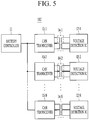
- FIG. 5 schematically illustrates a battery management system according to a conventional art.
- FIG. 6 illustrates a view for describing a reference potential difference between voltage detection ICs according to the conventional art.
- a conventional battery management system 10C includes a battery controller 11, a plurality of voltage detection ICs 12-1, 12-2, ..., 12-N, a plurality of CAN transceivers 13-1 and 13-2 ..., 13-N and a plurality of isolators 14-1, 14-2, ..., 14-N.
- the battery controller 10 receives a cell voltage of each cell constituting a high voltage battery (not illustrated) from the voltage detection ICs 12-1, 12-2, ..., and 12-N, to control charging and discharging of the high voltage battery.
- Each of voltage detection ICs 12-1, 12-2, ..., and 12-N is connected to a different cell stack, and includes a cell voltage detection circuit (not illustrated) for detecting a cell voltage of each cell constituting the corresponding cell stack.
- the cell stacks connected to the voltage detection ICs 12-1, 12-2, ..., and 12-N are connected in series to each other to constitute a high-voltage battery. Accordingly, reference potentials (DC levels) of the operation voltages may be different from each other between in view of a characteristic of the voltage detection ICs 12-1, 12-2, ..., and 12-N which receive operation voltages from the output voltages of the corresponding cell stack.
- each of the first and second cell stacks connected in series to each other include K cells connected in series with each other. Therefore, a reference potential GND2 of the second cell stack is higher than a reference potential GND1 of the first cell stack by K cell voltages Vbat11. Since the reference potentials GND1 and GND2 corresponding to the first and second cell stacks are different from each other, a potential difference is generated between the power voltages VDD1 and VDD2 of the voltage detection ICs corresponding to the respective cell stacks.
- the voltage detection ICs 12-1, 12-2, ..., and 12-N respectively include can transceivers CAN transceivers 13-1, 13-2, ..., and 13-N and isolators 14-1, 14-2, ..., and 14-N in the battery management system 10C according to the conventional art.
- the battery management system 10C needs to include N CAN transceivers 13-1, 13-2, ..., and 13-N and N isolators 14-1, 14-2, ..., and 14-N in order to perform the communication between the voltage detection ICs 12-1, 12-2, ..., and 12-N.
Landscapes
- Engineering & Computer Science (AREA)
- Power Engineering (AREA)
- Manufacturing & Machinery (AREA)
- Chemical & Material Sciences (AREA)
- Chemical Kinetics & Catalysis (AREA)
- Electrochemistry (AREA)
- General Chemical & Material Sciences (AREA)
- Transportation (AREA)
- Mechanical Engineering (AREA)
- Sustainable Development (AREA)
- Sustainable Energy (AREA)
- Life Sciences & Earth Sciences (AREA)
- Physics & Mathematics (AREA)
- General Physics & Mathematics (AREA)
- Microelectronics & Electronic Packaging (AREA)
- Secondary Cells (AREA)
- Measurement Of Current Or Voltage (AREA)
Abstract
Description
- An exemplary embodiment relate to a voltage detection integrated circuit, and a battery management system including the same.
- Recently, according to strengthening of environmental regulations including CO2 regulations, interest in environmentally-friendly vehicles has been increasing. Accordingly, vehicle companies have been actively researching and developing pure electrical vehicles and hydrogen vehicles, as well as hybrid and plug-in hybrid vehicles.
- A high voltage battery for storing electrical energy obtained from various energy sources is applied to the environmentally-friendly vehicles. A high voltage battery includes a plurality of cells in series or in parallel to provide high voltage electrical energy.
- A battery management system (BMS) for managing a high voltage battery is mounted in a vehicle to which the high voltage battery is applied. A cell balancing function which compensates a voltage deviation between cells by monitoring the voltage of each of the cells is one of the main functions of the battery management system. The voltage of each cell constituting the high voltage battery may be measured by an integrated circuit (IC), e.g., an analog front end (AFE) IC, having a built-in voltage detection circuit.
- DC levels may be different between ICs measuring cell voltages because of the structure of a high voltage battery in which a plurality of cells are stacked. For this reason, an isolator is essentially used for communication between voltage measurement ICs having different DC levels, and the use of an isolator increases a cost of the battery management system.
- An exemplary embodiment has been made in an effort to provide a battery management system that minimizes the use of an isolator.
- An exemplary embodiment of the present invention provides a battery management system including: a plurality of voltage detection integrated circuits; and a battery controller configured to control charge and discharge of a high voltage battery based on a cell voltage detection result received from the voltage detection integrated circuits, and each of the detection integrated circuits includes: a cell voltage detection circuit configured to detect a voltage of at least one corresponding cell among a plurality of cells constituting the high voltage battery; first and second interfaces configured to communicate between different voltage detection integrated circuits in the detection integrated circuits; a plurality of first terminals connected with a first power source which supplies an operation voltage of the cell voltage detection circuit and the first interface; a plurality of second terminals configured to receive an operation voltage of a different voltage detection integrated circuit connected therewith through the second interface; and a level shifter configured to level-shift a voltage supplied from the first power source based on the operation voltage inputted through the second terminals to supply the level-shifted voltage as an operation voltage of the second interface.
- In the battery management system, the first terminals may be connected with the second terminals of another voltage detection integrated circuit connected through the first interface among the plurality of voltage detection integrated circuits.
- In the battery management system, the first power source may be provided from the corresponding at least one cell.
- The battery management system may further include a transceiver configured to transmit and receive signals between the voltage detection integrated circuits and the battery controller, and an isolator connected between the transceiver and the second interface of one of the voltage detection circuits.
- In the battery management system, the level shifter may be deactivated in a voltage detection integrated circuit connected to the isolator among the plurality of voltage detection integrated circuits.
- In the battery management system, the first and second interfaces may communicate with other voltage detection integrated circuits in a daisy-chain method.
- An exemplary embodiment of the present invention provides an integrated circuit including: a cell voltage detection circuit configured to detect a cell voltage of at least one cell; first and second interfaces configured to communicate with other integrated circuits; a plurality of first power terminals connected with a first power source which supplies an operation voltage to the cell voltage detection circuits and the first interface; a plurality of second power terminals; and a level shifter configured to level-shift a voltage supplied from the first power source based on a voltage inputted through the second power terminals to supply the level-shifted voltage as an operation voltage of the second interface.
- In the integrated circuit, the second power terminals may be connected to power terminals of other integrated circuits that perform communication through the second interface.
- In the integrated circuit, the first power source may be provided from at least one cell connected to the cell voltage detection circuit.
- In the integrated circuit, the first and second interfaces may communicate with other voltage detection integrated circuits in a daisy-chain method.
- According to the exemplary embodiment of the present invention, it is possible to provide the battery management system which is capable of suppressing a unit price increase by minimizing the use of the isolator.
-
-
FIG. 1 schematically illustrates a voltage detection IC according to an exemplary embodiment. -
FIG. 2 illustrates an example of a battery management system including a voltage detection IC according to an exemplary embodiment. -
FIG. 3 illustrates a view for describing an operation of the battery management system ofFIG. 2 -
FIG. 4 illustrates another example of a battery management system including a voltage detection IC according to an exemplary embodiment. -
FIG. 5 schematically illustrates a battery management system according to a conventional art. -
FIG. 6 illustrates a view for describing a reference potential difference between voltage detection ICs according to the conventional art. - The present invention will be described more fully hereinafter with reference to the accompanying drawings, in which exemplary embodiments of the invention are shown. As those skilled in the art would realize, the described embodiments may be modified in various different ways, all without departing from the spirit or scope of the present invention.
- To clearly describe the exemplary embodiments, parts that are irrelevant to the description are omitted, and like numerals refer to like or similar constituent elements throughout the specification. Therefore, the reference numbers of the constituent elements used in a previous drawing may be used in a next drawing.
- Further, since sizes and thicknesses of constituent members shown in the accompanying drawings are arbitrarily given for better understanding and ease of description, the exemplary embodiments are not limited to the illustrated sizes and thicknesses. In the drawings, the thickness of layers, films, panels, regions, etc., are exaggerated for clarity.
- A case of electrically connecting two constituent elements includes not only a case of directly connecting the constituent elements but also a case of connecting the constituent elements via another constituent element therebetween. The constituent element therebetween may include a switch, a resistor, a capacitor, and the like. In describing exemplary embodiments, an expression of connection indicates electrical connection unless explicitly described to be direct connection.
- Hereinafter, a voltage detection integrated circuit (IC) according to exemplary embodiments and a battery management system including the same will be described in detail with reference to the drawings. In this document, the voltage detection IC may include an analog front end (AFE) IC including a cell voltage detection function of a battery, a cell voltage monitoring (CVM) IC, and the like.
-
FIG. 1 schematically illustrates a voltage detection IC according to an exemplary embodiment. - Referring to
FIG. 1 , avoltage detection IC 120 according to the present exemplary embodiment may include alevel shifter 121,communication circuits voltage detection circuit 123, acontroller 124, and a plurality of power terminals GND_L, VDD_L GND_H, and VDD_H. - Each of the communication circuits serves to communicate with another voltage detection IC or a battery controller (see
reference numeral 110 inFIG. 2 ). The communication circuits may include a plurality ofinterfaces reference numeral 110 inFIG. 2 ). - Each of the
interfaces - The cell
voltage detection circuit 123 may be electrically connected to at least one cell constituting a cell stack 20, and a cell voltage of each of the cells may be measured. The cellvoltage detection circuit 123 may include an analog-to-digital converter (ADC) for converting the cell voltage of each cell detected as an analog value into a digital value. - The
controller 124, which is a controller in the IC, may control the cellvoltage detection circuit 123 and a daisy chain communication circuit 122. For example, the cellvoltage detection circuit 123 may be controlled to select a target cell, a voltage of which is to be detected, among the cells constituting the cell stack 20. Further, for example, the cell voltage detected by the cellvoltage detection circuit 123 may be transferred to the battery controller (seereference numeral 110 inFIG. 2 ) through the daisy chain communication circuit 122. - Different power supplies are connected to the first power terminals GND_L and VDD_L and the second power terminals GND_H and VDD_H. For convenience of description, hereinafter, the power source that is connected to the first power terminals GND_L and VDD_L is referred to as a first power source, and the power source that is connected to the second power terminals GND_H and VDD_H is referred to as a second power source.
- The first power source, which is a main operation power source, supplies an operation voltage to the ADC of the cell
voltage detection circuit 123, thecontroller 124, and thefirst interface 1221 of thevoltage detection IC 120. - The first power source may be provided from a power supply circuit outside the
voltage detection IC 120, or may be provided from a power supply circuit inside thevoltage detection IC 120. In the latter case, the power supply circuit in thevoltage detection IC 120 can provide the first power source by transforming the cell voltage supplied from at least one cell of the cell stack 20. - The second power source is a power source that is a reference for level shifting of the
level shifter 121. - As the second power, the first power of another voltage detection IC may be used. In this case, the second power terminals GND_H and VDD_H may be connected to the first power terminals GND_L and VDD_L of the voltage detection IC to be communicated through the
second interface 1222. The second power may be a common power that is commonly supplied to all the voltage detection ICs. In this case, the second power terminals GND_H and VDD_H may be connected to the second power terminals GND_H and VDD_H of another voltage detection IC. - The
level shifter 121 may receive the first power and the second power from the first power terminals GND_L and VDD_L and the second power terminals GND_H and VDD_H, to level-shift a reference potential (DC level) of the first power to a reference potential (DC level) of the second power. That is, thelevel shifter 121 may level-shift the operation voltage supplied from the first power source to the operation voltage of the second power source. - The operation voltage level-shifted by the
level shifter 121 may be supplied as the operation voltage of thesecond interface 1222. - Accordingly, the
second interface 1222 of thevoltage detection IC 120 may be operated by receiving an operation voltage of a same level as that of the voltage detection IC to be communicated by thelevel shifter 121, so that communication between thevoltage detection IC 120 and another voltage detection IC may be performed without an isolator. -
FIG. 2 illustrates an example of a battery management system including a voltage detection IC according to an exemplary embodiment, andFIG. 3 illustrates a view for describing an operation of the battery management system ofFIG. 2 - Referring to
FIG. 2 , abattery management system 10A according to a first exemplary embodiment may include abattery controller 110, a plurality of voltage detection ICs 120-1, 120-2, and 120-3, atransceiver 130, and anisolator 140. Although a case where thebattery management system 10A includes three voltage detection ICs is illustrated as an example inFIG. 2 , the present invention is not limited thereto, and a number of voltage detection ICs included in thebattery management system 10A may be more or less than three. - The
battery controller 110 may receive a cell voltage of each cell constituting a high voltage battery (not shown) from the voltage detection ICs 120-1, 120-2, and 120-3, to control charging and discharging of the respective cells or the high voltage battery. - The voltage detection ICs 120-1, 120-2, and 120-3 may be respectively connected to cell stacks (see reference numeral 20 in
FIG. 1 ) connected in series with each other, to detect a cell voltage of each cell constituting a corresponding cell stack. - The voltage detection ICs 120-1, 120-2, and 120-3 respectively include first and second interfaces 1221-1, 1221-2, and 1221-3, and 1222-1, 1222-2, and 1222-3, and level shifters 121-1, 121-2, and 121-3.
- The first interfaces 1221-1, 1221-2, and 1221-3 may respectively receive operation voltages through the first power terminals GND_L1 and VDD_L1, GND_L2 and VDD_L2, and GND_L3 and VDD_L3.
- The second interfaces 1222-1, 1222-2, and 1222-3 may respectively receive operation voltages from the level shifters 121-1, 121-2, and 121-3.
- The level shifters 121-1, 121-2, and 121-3 respectively level-shift and output voltages supplied to the first power terminals GND_L1 and VDD_L1, GND_L2 and VDD_L2, and GND_L3 and VDD_L3 based on voltages inputted through the second power terminals GND_H1 and VDD_H1, GND_H2 and VDD_H2, and GND_H3 and VDD_H3 of the voltage detection ICs 120-1, 120-2, and 120-3. The voltages level-shifted by the level shifters 121-1, 121-2, and 121-3 may be respectively supplied as operation voltages of the corresponding second interfaces 1222-1, 1222-2, and 1222-3.
- The first interface 1221-1 of the first voltage detection IC 120-1 receives a voltage applied to the first power terminals GND_L1 and VDD_L1 as an operation voltage. The second interface 1222-1 receives a voltage that is level-shifted through the level shifter 121-1 as the operation voltage. The second power terminals GND_H1 and VDD_H1 are connected to the first power terminals GND_L2 and VDD_L2 of the second voltage detection IC 120-2 which is an upper voltage detection IC of the first voltage detection IC 120-1, to receive an operation voltage of the first interface 1221-2 of the second voltage detection IC 120-2. Accordingly, the level shifter 121-1 may supply a voltage that is level-shifted to the operation voltage of the first interface 1221-2 of the second voltage detection IC 120-2 as an operation voltage of the second interface 1222-1.
- For example, referring to
FIG. 3 , a potential difference occurs between main operation voltages of the first voltage detection IC 120-1 and the second voltage detection IC 120-2 by an output voltage Vbat1 of the first cell stack connected with the first voltage detection IC 120-1. Accordingly, the level shifter 121-1 of the first voltage detecting IC 120-1 level-shifts a voltage applied to the first power terminals GND_L1 and VDD_L1 by the output voltage Vbat1 of the first cell stack to supply it as an operation voltage of the second interface 1222-1. - This enables communication between the second interface 1222-1 of the first voltage detection IC 120-1 and the first interface 1221-2 of the second voltage detection IC 120-2 without an isolator.
- In this document, in describing positions between the voltage detection ICs, 'upper' or 'lower' may be defined depending on positions in the high voltage battery of the cell stack connected with each of the voltage detection IC. For example, when a cell stack connected to the first voltage detection IC 120-1 is connected closer to the ground than a cell stack connected to the second voltage detection IC 120-2, the first voltage detection IC 120-1 may be expressed as a lower voltage detection IC of the second voltage detection IC 120-2, and the second voltage detection IC 120-2 may be expressed as an upper voltage detection IC of the first voltage detection IC 120-1.
- Referring again to
FIG. 2 , the first interface 1221-2 of the second voltage detection IC 120-2 receives a voltage applied to the first power terminals GND_L2 and VDD_L2 as an operation voltage. The second interface 1222-2 receives a voltage that is level-shifted through the level shifter 121-2 as the operation voltage. The second power terminals GND_H2 and VDD_H2 are connected to the first power terminals GND_L3 and VDD_L3 of the second voltage detection IC 120-3 which is an upper voltage detection IC of the first voltage detection IC 120-2, to receive an operation voltage of the first interface 1221-3 of the third voltage detection IC 120-3. Accordingly, the level shifter 121-2 may supply a voltage that is level-shifted to the operation voltage of the first interface 1221-3 of the third voltage detection IC 120-2 as an operation voltage of the second interface 1222-1. - For example, referring to
FIG. 3 , a potential difference occurs between main operation voltages of the second voltage detection IC 120-2 and the third voltage detection IC 120-3 by an output voltage Vbat2 of the second cell stack connected with the second voltage detection IC 120-2. Accordingly, the level shifter 121-2 of the second voltage detecting IC 120-2 level-shifts a voltage applied to the first power terminals GND_L2 and VDD_L2 by the output voltage Vbat2 of the second cell stack to supply it as an operation voltage of the second interface 1222-2. - This enables communication between the second interface 1222-2 of the first voltage detection IC 120-2 and the first interface 1221-3 of the third voltage detection IC 120-3 without an isolator.
- Referring again to
FIG. 2 , the third voltage detection IC 120-3 is the voltage detection IC of a final stage which is most closely connected to thebattery controller 110 in a daisy chain bus, and thus the level shifter 121-3 for communicating with the upper voltage detection IC is inactivated. Thus, both the first interface 1221-3 and the second interface 1222-3 of the third voltage detecting IC 120-3 receive a voltage applied to the first power terminals GND_L2 and VDD_L2 as an operation voltage. - The second interface 1222-2 of the third voltage detection IC 120-3 communicates with the
battery controller 110 via thetransceiver 130 and theisolator 140, since the third voltage detection IC 120-3 is disposed at the final stage of the daisy chain bus. - The
transceiver 130 may transmit and receive signals to and from thebattery controller 110 through a serial peripheral interface (SPI).FIG. 2 shows an example in which the SPI is a controller area network (CAN) communication. - A potential difference exists between operation voltages of the
transceiver 130 and the third voltage detecting IC 120-3 so that anisolator 140 for solving the potential difference may be connected between thetransceiver 130 and the second interface 1222-2 of the third voltage detection IC 120-3. - Although a case where the third voltage detection IC 120-3 is connected to an uppermost cell stack of the high voltage battery so that the level shifters 121-1 and 121-2 of the first and second voltage detection ICs 120-1 and 120-2 up-shift voltage levels is described as an example in
FIG. 2 andFIG. 3 , the present invention is not limited thereto, and the third voltage detection IC 120-3 may be connected to a lowermost cell stack of the high voltage battery. In this case, the level shifters 121-1 and 121-2 of the first and second voltage detection ICs 120-1 and 120-2 may down-shift the voltage levels depending on the operation voltage of lower voltage detection ICs thereof so as to supply them as operation voltages of the second interfaces 1222-1 and 1222-2. - In addition, although a case where a voltage detection IC (the third voltage detection IC 120-3 of
FIG. 3 ) connected to the uppermost cell stack is disposed at the final stage of the daisy chain bus to communicate with thebattery controller 110 is described as an example inFIG. 2 andFIG. 3 , the present invention is not limited thereto. According to another exemplary embodiment, a voltage detection IC (the first voltage detection IC 120-1 in the case ofFIG. 2 ) connected to the lowermost cell stack may be disposed at the final stage of the daisy chain bus to communicate with thebattery controller 110. In this case, thebattery controller 110 may be connected to the first interface 1221-1 of the voltage detection IC 120-1 connected to the lowermost cell stack through thetransceiver 130 and theisolator 140. As described above, thebattery management system 10A does not need to use an isolator for communication between the voltage detection ICs 120-1, 120-2, and 120-3. Therefore, the number of isolators mounted in thebattery management system 10A may be minimized, thereby reducing the cost. - Recently, a method for applying a system in package (SIP) technology to a voltage detection IC has been studied to improve channel scalability. The SIP is a technology for packaging a plurality of voltage detecting ICs into a single chip package, which is advantageous in that the development cost is low and the chip configuration of various channels is easy.
-
FIG. 4 illustrates another example of a battery management system including a voltage detection IC, to which SIP technology is applied, according to an exemplary embodiment. - Referring to
FIG. 4 , the battery management system 10B includes a plurality of voltage detection IC packages SIP1 and SIP2, and each of the voltage detection IC packages SIP1 and SIP2 may be configured by packaging a plurality of voltage detection ICs (120-12, 120-13, 120-21, 120-22, ...). - The voltage detecting ICs included in one voltage detecting IC package SIP1 or SIP2 may communicate with each other without an isolator by using the level shift method described with reference to
FIG. 1 to FIG. 3 described above. - For example, the voltage detection IC 120-21 of the second voltage detection IC package SIP2 receives an operation voltage of the upper voltage detection IC 120-22 from its upper voltage detection IC 120-22, and level-shifts a main operation voltage of the voltage detection IC 120-21 based on the received operation voltage. In addition, it is possible to communicate with the voltage detection IC without an isolator by supplying the level-shifted voltage as an operation voltage of the second interface 1222-21 which communicates with the voltage detection IC 120-22.
- Even when communication is desired to be performed between the voltage detection IC packages SIP1 and SIP2 without an isolator in a battery management system 10B, the communication may be performed there between without an isolator by using the level shift method described with reference to
FIG. 1 to FIG. 3 . In this case, a main operation voltage of the lowermost voltage detection IC 120-21 of the second voltage detection IC package SIP2 is supplied to a level shifter 121-13 of the uppermost voltage detection IC 120-13 of the first voltage detection IC package SIP1. Accordingly, the level shifter 121-13 of the voltage detection IC 120-3 level-shifts a main operation voltage of the voltage detection IC 120-13 based on the main operation voltage of the lowermost voltage detection IC 120-21 or the second voltage detection IC package SIP2. In addition, the communication between the voltage detection IC packages SIP1 and SIP2 may be performed without an isolator by supplying the level-shifted voltage as an operation voltage of the second interface 1222-3 which communicates with the second voltage detection IC package SIP2. - As described above, according to an exemplary embodiment, a voltage detection IC (see
reference numeral 120 inFIG. 1 ) may be expanded and applied to a case where a plurality of voltage detection ICs are packaged in one SIP as well as the case where one voltage detection IC is packaged in one package. -
FIG. 5 schematically illustrates a battery management system according to a conventional art.FIG. 6 illustrates a view for describing a reference potential difference between voltage detection ICs according to the conventional art. - Referring to
FIG. 5 , a conventionalbattery management system 10C includes abattery controller 11, a plurality of voltage detection ICs 12-1, 12-2, ..., 12-N, a plurality of CAN transceivers 13-1 and 13-2 ..., 13-N and a plurality of isolators 14-1, 14-2, ..., 14-N. - The battery controller 10 receives a cell voltage of each cell constituting a high voltage battery (not illustrated) from the voltage detection ICs 12-1, 12-2, ..., and 12-N, to control charging and discharging of the high voltage battery.
- Each of voltage detection ICs 12-1, 12-2, ..., and 12-N is connected to a different cell stack, and includes a cell voltage detection circuit (not illustrated) for detecting a cell voltage of each cell constituting the corresponding cell stack.
- The cell stacks connected to the voltage detection ICs 12-1, 12-2, ..., and 12-N are connected in series to each other to constitute a high-voltage battery. Accordingly, reference potentials (DC levels) of the operation voltages may be different from each other between in view of a characteristic of the voltage detection ICs 12-1, 12-2, ..., and 12-N which receive operation voltages from the output voltages of the corresponding cell stack.
- For example, referring to
FIG. 6 , each of the first and second cell stacks connected in series to each other include K cells connected in series with each other. Therefore, a reference potential GND2 of the second cell stack is higher than a reference potential GND1 of the first cell stack by K cell voltages Vbat11. Since the reference potentials GND1 and GND2 corresponding to the first and second cell stacks are different from each other, a potential difference is generated between the power voltages VDD1 and VDD2 of the voltage detection ICs corresponding to the respective cell stacks. - As the potential difference is generated between the voltage detecting ICs 12-1, 12-2, ..., and 12-N as described above, the voltage detection ICs 12-1, 12-2, ..., and 12-N respectively include can transceivers CAN transceivers 13-1, 13-2, ..., and 13-N and isolators 14-1, 14-2, ..., and 14-N in the
battery management system 10C according to the conventional art. That is, when N voltage detection ICs 12-1, 12-2, ..., and 12-N are included in thebattery management system 10C, thebattery management system 10C needs to include N CAN transceivers 13-1, 13-2, ..., and 13-N and N isolators 14-1, 14-2, ..., and 14-N in order to perform the communication between the voltage detection ICs 12-1, 12-2, ..., and 12-N. - As described above, when a CAN transceiver and an isolator are provided for each of the voltage detection ICs, the use of a comparatively expensive isolator increases, and thus the unit price of the battery management system rises.
- In contrast, in accordance with the battery management system according to the exemplary embodiment described with reference to
FIG. 1 to FIG. 4 , it is possible to reduce the cost of the battery management system by decreasing the use of the isolator compared to the conventional art. - While exemplary embodiments of the present invention have been particularly shown and described with reference to the accompanying drawings, the specific terms used herein are only for the purpose of describing the invention and are not intended to define the meanings thereof or be limiting of the scope of the invention set forth in the claims. Therefore, those skilled in the art will understand that various modifications and other equivalent embodiments of the present invention are possible. Consequently, the true technical protective scope of the present invention must be determined based on the technical spirit of the appended claims.
-
- 10A, 10B: battery management system
- 110: battery controller
- 120: voltage detection integrated circuit
- 121: level shifter
- 1221, 1222: interface
- 123: cell voltage detection circuit
- 124: controller
- 130: transceiver
- 140: isolator
Claims (10)
- A battery management system comprising:a plurality of voltage detection integrated circuits; anda battery controller configured to control charge and discharge of a high voltage battery based on a cell voltage detection result received from the voltage detection integrated circuits, andeach of the detection integrated circuits includes:a cell voltage detection circuit configured to detect a voltage of at least one corresponding cell among a plurality of cells constituting the high voltage battery;first and second interfaces configured to communicate between different voltage detection integrated circuits in the detection integrated circuits;a plurality of first terminals connected with a first power source which supplies an operation voltage of the cell voltage detection circuit and the first interface;a plurality of second terminals configured to receive an operation voltage of a different voltage detection integrated circuit connected therewith through the second interface; anda level shifter configured to level-shift a voltage supplied from the first power source based on the operation voltage inputted through the second terminals to supply the level-shifted voltage as an operation voltage of the second interface.
- The battery management system of claim 1, wherein
the first terminals are connected with the second terminals of another voltage detection integrated circuit connected through the first interface among the plurality of voltage detection integrated circuits. - The battery management system of claim 1, wherein
the first power source is supplied from the corresponding at least one cell. - The battery management system of claim 1, further comprising:a transceiver configured to transmit and receive signals between the voltage detection integrated circuits and the battery controller; andan isolator connected between the transceiver and the second interface of one of the voltage detection circuits.
- The battery management system of claim 4, wherein
the level shifter is deactivated in a voltage detection integrated circuit connected to the isolator among the plurality of voltage detection integrated circuits. - The battery management system of claim 1, wherein
the first and second interfaces communicate with other voltage detection integrated circuits in a daisy-chain method. - An integrated circuit comprising:a cell voltage detection circuit configured to detect a cell voltage of at least one cell;first and second interfaces configured to communicate with other integrated circuits;a plurality of first power terminals connected with a first power source which supplies an operation voltage to the cell voltage detection circuits and the first interface;a plurality of second power terminals; anda level shifter configured to level-shift a voltage supplied from the first power source based on a voltage inputted through the second power terminals to supply the level-shifted voltage as an operation voltage of the second interface.
- The integrated circuit of claim 7, wherein
the second power terminals are connected to power terminals of other integrated circuits that perform communication through the second interface. - The integrated circuit of claim 7, wherein
the first power source is supplied from at least one cell connected to the cell voltage detection circuit. - The integrated circuit of claim 7, wherein
the first and second interfaces communicate with other voltage detection integrated circuits in a daisy-chain method.
Applications Claiming Priority (2)
| Application Number | Priority Date | Filing Date | Title |
|---|---|---|---|
| KR1020160176862A KR102249887B1 (en) | 2016-12-22 | 2016-12-22 | Voltage detecting ic and battery management system including the same |
| PCT/KR2017/011605 WO2018117387A2 (en) | 2016-12-22 | 2017-10-19 | Voltage detection integrated circuit and battery management system including same |
Publications (3)
| Publication Number | Publication Date |
|---|---|
| EP3560748A2 true EP3560748A2 (en) | 2019-10-30 |
| EP3560748A4 EP3560748A4 (en) | 2020-08-05 |
| EP3560748B1 EP3560748B1 (en) | 2023-12-06 |
Family
ID=62626722
Family Applications (1)
| Application Number | Title | Priority Date | Filing Date |
|---|---|---|---|
| EP17883666.4A Active EP3560748B1 (en) | 2016-12-22 | 2017-10-19 | Voltage detection integrated circuit and battery management system including same |
Country Status (7)
| Country | Link |
|---|---|
| US (1) | US11322951B2 (en) |
| EP (1) | EP3560748B1 (en) |
| KR (1) | KR102249887B1 (en) |
| CN (1) | CN110139777B (en) |
| HU (1) | HUE065333T2 (en) |
| PL (1) | PL3560748T3 (en) |
| WO (1) | WO2018117387A2 (en) |
Families Citing this family (4)
| Publication number | Priority date | Publication date | Assignee | Title |
|---|---|---|---|---|
| KR20200100967A (en) | 2019-02-19 | 2020-08-27 | 주식회사 엘지화학 | Integrated circuit chip and circuit system using the same |
| CN111864281B (en) * | 2020-05-14 | 2024-08-20 | 广东锂纬科技有限公司 | Lithium battery management system |
| KR102579043B1 (en) * | 2021-08-18 | 2023-09-15 | 한국과학기술원 | Architecture for measurement system designed for massive impedance extraction of battery systems |
| JP2025066055A (en) * | 2023-10-10 | 2025-04-22 | 恵州億緯▲リ▼能股▲フン▼有限公司 | Electrical Modules and Battery Packs |
Family Cites Families (15)
| Publication number | Priority date | Publication date | Assignee | Title |
|---|---|---|---|---|
| JP3775587B2 (en) * | 2002-02-14 | 2006-05-17 | 株式会社デンソー | Battery status monitoring device for fuel cell stack |
| JP5028436B2 (en) * | 2009-01-27 | 2012-09-19 | 株式会社日立製作所 | Battery controller potential fixing method |
| JP5537364B2 (en) * | 2009-09-30 | 2014-07-02 | 株式会社東芝 | Communication circuit, assembled battery device and vehicle |
| JP5453184B2 (en) | 2010-06-28 | 2014-03-26 | 日立ビークルエナジー株式会社 | Battery control circuit |
| JP5638311B2 (en) * | 2010-08-18 | 2014-12-10 | ラピスセミコンダクタ株式会社 | Battery pack system, voltage monitoring system, voltage monitoring device, and semiconductor device |
| DE102010040713A1 (en) * | 2010-09-14 | 2012-03-15 | Sb Limotive Company Ltd. | Battery with detection of cell voltages and battery current and only one potential separation device |
| JP2012065518A (en) * | 2010-09-17 | 2012-03-29 | Toshiba Corp | Battery pack module, secondary battery device, and vehicle |
| EP3699617B1 (en) * | 2011-10-07 | 2024-02-07 | Hitachi Astemo, Ltd. | Battery monitoring apparatus and battery monitoring system |
| JP5798887B2 (en) * | 2011-10-31 | 2015-10-21 | 株式会社日立製作所 | Power storage system |
| KR20130065351A (en) * | 2011-12-09 | 2013-06-19 | 현대오트론 주식회사 | Battery management system using daisy-chain scheme |
| CN103358926B (en) * | 2012-03-30 | 2016-12-28 | 拉碧斯半导体株式会社 | Battery monitoring system and semiconductor device |
| JP6168803B2 (en) | 2012-03-30 | 2017-07-26 | ラピスセミコンダクタ株式会社 | Battery monitoring system and semiconductor device |
| JP6193573B2 (en) * | 2013-01-10 | 2017-09-06 | ラピスセミコンダクタ株式会社 | Battery monitoring system, battery monitoring device, and battery monitoring system activation method |
| US20150102943A1 (en) | 2013-10-10 | 2015-04-16 | Datang Nxp Semiconductors Co., Ltd. | Daisy-chain communication bus and protocol |
| JP6479320B2 (en) | 2014-02-25 | 2019-03-06 | ラピスセミコンダクタ株式会社 | Battery monitoring system and battery monitoring chip |
-
2016
- 2016-12-22 KR KR1020160176862A patent/KR102249887B1/en active Active
-
2017
- 2017-10-19 EP EP17883666.4A patent/EP3560748B1/en active Active
- 2017-10-19 WO PCT/KR2017/011605 patent/WO2018117387A2/en not_active Ceased
- 2017-10-19 HU HUE17883666A patent/HUE065333T2/en unknown
- 2017-10-19 US US16/467,893 patent/US11322951B2/en active Active
- 2017-10-19 CN CN201780079524.6A patent/CN110139777B/en active Active
- 2017-10-19 PL PL17883666.4T patent/PL3560748T3/en unknown
Also Published As
| Publication number | Publication date |
|---|---|
| US11322951B2 (en) | 2022-05-03 |
| KR20180073241A (en) | 2018-07-02 |
| KR102249887B1 (en) | 2021-05-07 |
| EP3560748A4 (en) | 2020-08-05 |
| CN110139777B (en) | 2022-11-08 |
| WO2018117387A2 (en) | 2018-06-28 |
| HUE065333T2 (en) | 2024-05-28 |
| US20200091735A1 (en) | 2020-03-19 |
| CN110139777A (en) | 2019-08-16 |
| EP3560748B1 (en) | 2023-12-06 |
| PL3560748T3 (en) | 2024-05-13 |
| WO2018117387A3 (en) | 2018-08-16 |
Similar Documents
| Publication | Publication Date | Title |
|---|---|---|
| US10630067B2 (en) | Semiconductor device and battery voltage monitoring device | |
| EP2132855B1 (en) | Monitoring cells in energy storage system | |
| EP3560748B1 (en) | Voltage detection integrated circuit and battery management system including same | |
| EP1806592B1 (en) | Method and system for monitoring battery stacks | |
| US7248020B2 (en) | Battery-voltage monitoring integrated-circuit and battery-voltage monitoring system | |
| US9478980B2 (en) | System for balancing, by magnetic coupling, an association in series of elements for generating or storing electrical energy | |
| US8227944B2 (en) | Vertical bus circuits | |
| US8970163B2 (en) | Charge control system of battery pack | |
| CN107390117B (en) | Switch high-voltage sampling circuit for electric vehicle | |
| US11001150B2 (en) | Battery pack | |
| US9368980B2 (en) | Battery control circuit | |
| US20150061597A1 (en) | Battery management system and method | |
| CN109565086B (en) | Power storage system | |
| US7893715B2 (en) | Arrangement and method for signal transmission between different voltage domains | |
| US10067196B2 (en) | Voltage measuring apparatus |
Legal Events
| Date | Code | Title | Description |
|---|---|---|---|
| STAA | Information on the status of an ep patent application or granted ep patent |
Free format text: STATUS: THE INTERNATIONAL PUBLICATION HAS BEEN MADE |
|
| PUAI | Public reference made under article 153(3) epc to a published international application that has entered the european phase |
Free format text: ORIGINAL CODE: 0009012 |
|
| STAA | Information on the status of an ep patent application or granted ep patent |
Free format text: STATUS: REQUEST FOR EXAMINATION WAS MADE |
|
| 17P | Request for examination filed |
Effective date: 20190521 |
|
| AK | Designated contracting states |
Kind code of ref document: A2 Designated state(s): AL AT BE BG CH CY CZ DE DK EE ES FI FR GB GR HR HU IE IS IT LI LT LU LV MC MK MT NL NO PL PT RO RS SE SI SK SM TR |
|
| AX | Request for extension of the european patent |
Extension state: BA ME |
|
| DAV | Request for validation of the european patent (deleted) | ||
| DAX | Request for extension of the european patent (deleted) | ||
| A4 | Supplementary search report drawn up and despatched |
Effective date: 20200708 |
|
| RIC1 | Information provided on ipc code assigned before grant |
Ipc: H02J 7/00 20060101ALI20200702BHEP Ipc: G01R 31/36 20200101ALI20200702BHEP Ipc: B60L 3/00 20190101AFI20200702BHEP Ipc: H01M 10/42 20060101ALI20200702BHEP |
|
| RIN1 | Information on inventor provided before grant (corrected) |
Inventor name: KIM, YONGCHUN Inventor name: CHO, WONKYOUNG |
|
| STAA | Information on the status of an ep patent application or granted ep patent |
Free format text: STATUS: EXAMINATION IS IN PROGRESS |
|
| 17Q | First examination report despatched |
Effective date: 20210924 |
|
| REG | Reference to a national code |
Ref country code: DE Ref legal event code: R079 Free format text: PREVIOUS MAIN CLASS: B60L0003000000 Ref country code: DE Ref legal event code: R079 Ref document number: 602017077351 Country of ref document: DE Free format text: PREVIOUS MAIN CLASS: B60L0003000000 Ipc: B60L0058180000 |
|
| RIC1 | Information provided on ipc code assigned before grant |
Ipc: H02J 7/00 20060101ALI20230503BHEP Ipc: H01M 10/48 20060101ALI20230503BHEP Ipc: H01M 10/44 20060101ALI20230503BHEP Ipc: G01R 31/396 20190101ALI20230503BHEP Ipc: G01R 19/165 20060101ALI20230503BHEP Ipc: B60L 58/22 20190101ALI20230503BHEP Ipc: B60L 58/18 20190101AFI20230503BHEP |
|
| GRAP | Despatch of communication of intention to grant a patent |
Free format text: ORIGINAL CODE: EPIDOSNIGR1 |
|
| STAA | Information on the status of an ep patent application or granted ep patent |
Free format text: STATUS: GRANT OF PATENT IS INTENDED |
|
| INTG | Intention to grant announced |
Effective date: 20230726 |
|
| INTG | Intention to grant announced |
Effective date: 20230726 |
|
| GRAS | Grant fee paid |
Free format text: ORIGINAL CODE: EPIDOSNIGR3 |
|
| GRAA | (expected) grant |
Free format text: ORIGINAL CODE: 0009210 |
|
| STAA | Information on the status of an ep patent application or granted ep patent |
Free format text: STATUS: THE PATENT HAS BEEN GRANTED |
|
| AK | Designated contracting states |
Kind code of ref document: B1 Designated state(s): AL AT BE BG CH CY CZ DE DK EE ES FI FR GB GR HR HU IE IS IT LI LT LU LV MC MK MT NL NO PL PT RO RS SE SI SK SM TR |
|
| REG | Reference to a national code |
Ref country code: GB Ref legal event code: FG4D |
|
| REG | Reference to a national code |
Ref country code: DE Ref legal event code: R096 Ref document number: 602017077351 Country of ref document: DE |
|
| REG | Reference to a national code |
Ref country code: CH Ref legal event code: EP |
|
| REG | Reference to a national code |
Ref country code: IE Ref legal event code: FG4D |
|
| REG | Reference to a national code |
Ref country code: SE Ref legal event code: TRGR |
|
| REG | Reference to a national code |
Ref country code: LT Ref legal event code: MG9D |
|
| PG25 | Lapsed in a contracting state [announced via postgrant information from national office to epo] |
Ref country code: GR Free format text: LAPSE BECAUSE OF FAILURE TO SUBMIT A TRANSLATION OF THE DESCRIPTION OR TO PAY THE FEE WITHIN THE PRESCRIBED TIME-LIMIT Effective date: 20240307 |
|
| REG | Reference to a national code |
Ref country code: NL Ref legal event code: MP Effective date: 20231206 |
|
| PG25 | Lapsed in a contracting state [announced via postgrant information from national office to epo] |
Ref country code: LT Free format text: LAPSE BECAUSE OF FAILURE TO SUBMIT A TRANSLATION OF THE DESCRIPTION OR TO PAY THE FEE WITHIN THE PRESCRIBED TIME-LIMIT Effective date: 20231206 |
|
| PG25 | Lapsed in a contracting state [announced via postgrant information from national office to epo] |
Ref country code: ES Free format text: LAPSE BECAUSE OF FAILURE TO SUBMIT A TRANSLATION OF THE DESCRIPTION OR TO PAY THE FEE WITHIN THE PRESCRIBED TIME-LIMIT Effective date: 20231206 |
|
| PG25 | Lapsed in a contracting state [announced via postgrant information from national office to epo] |
Ref country code: LT Free format text: LAPSE BECAUSE OF FAILURE TO SUBMIT A TRANSLATION OF THE DESCRIPTION OR TO PAY THE FEE WITHIN THE PRESCRIBED TIME-LIMIT Effective date: 20231206 Ref country code: GR Free format text: LAPSE BECAUSE OF FAILURE TO SUBMIT A TRANSLATION OF THE DESCRIPTION OR TO PAY THE FEE WITHIN THE PRESCRIBED TIME-LIMIT Effective date: 20240307 Ref country code: ES Free format text: LAPSE BECAUSE OF FAILURE TO SUBMIT A TRANSLATION OF THE DESCRIPTION OR TO PAY THE FEE WITHIN THE PRESCRIBED TIME-LIMIT Effective date: 20231206 Ref country code: BG Free format text: LAPSE BECAUSE OF FAILURE TO SUBMIT A TRANSLATION OF THE DESCRIPTION OR TO PAY THE FEE WITHIN THE PRESCRIBED TIME-LIMIT Effective date: 20240306 |
|
| PG25 | Lapsed in a contracting state [announced via postgrant information from national office to epo] |
Ref country code: NL Free format text: LAPSE BECAUSE OF FAILURE TO SUBMIT A TRANSLATION OF THE DESCRIPTION OR TO PAY THE FEE WITHIN THE PRESCRIBED TIME-LIMIT Effective date: 20231206 |
|
| REG | Reference to a national code |
Ref country code: HU Ref legal event code: AG4A Ref document number: E065333 Country of ref document: HU |
|
| PG25 | Lapsed in a contracting state [announced via postgrant information from national office to epo] |
Ref country code: RS Free format text: LAPSE BECAUSE OF FAILURE TO SUBMIT A TRANSLATION OF THE DESCRIPTION OR TO PAY THE FEE WITHIN THE PRESCRIBED TIME-LIMIT Effective date: 20231206 Ref country code: NO Free format text: LAPSE BECAUSE OF FAILURE TO SUBMIT A TRANSLATION OF THE DESCRIPTION OR TO PAY THE FEE WITHIN THE PRESCRIBED TIME-LIMIT Effective date: 20240306 Ref country code: NL Free format text: LAPSE BECAUSE OF FAILURE TO SUBMIT A TRANSLATION OF THE DESCRIPTION OR TO PAY THE FEE WITHIN THE PRESCRIBED TIME-LIMIT Effective date: 20231206 Ref country code: LV Free format text: LAPSE BECAUSE OF FAILURE TO SUBMIT A TRANSLATION OF THE DESCRIPTION OR TO PAY THE FEE WITHIN THE PRESCRIBED TIME-LIMIT Effective date: 20231206 Ref country code: HR Free format text: LAPSE BECAUSE OF FAILURE TO SUBMIT A TRANSLATION OF THE DESCRIPTION OR TO PAY THE FEE WITHIN THE PRESCRIBED TIME-LIMIT Effective date: 20231206 |
|
| PG25 | Lapsed in a contracting state [announced via postgrant information from national office to epo] |
Ref country code: IS Free format text: LAPSE BECAUSE OF FAILURE TO SUBMIT A TRANSLATION OF THE DESCRIPTION OR TO PAY THE FEE WITHIN THE PRESCRIBED TIME-LIMIT Effective date: 20240406 |
|
| PG25 | Lapsed in a contracting state [announced via postgrant information from national office to epo] |
Ref country code: CZ Free format text: LAPSE BECAUSE OF FAILURE TO SUBMIT A TRANSLATION OF THE DESCRIPTION OR TO PAY THE FEE WITHIN THE PRESCRIBED TIME-LIMIT Effective date: 20231206 |
|
| PG25 | Lapsed in a contracting state [announced via postgrant information from national office to epo] |
Ref country code: SK Free format text: LAPSE BECAUSE OF FAILURE TO SUBMIT A TRANSLATION OF THE DESCRIPTION OR TO PAY THE FEE WITHIN THE PRESCRIBED TIME-LIMIT Effective date: 20231206 |
|
| PG25 | Lapsed in a contracting state [announced via postgrant information from national office to epo] |
Ref country code: SM Free format text: LAPSE BECAUSE OF FAILURE TO SUBMIT A TRANSLATION OF THE DESCRIPTION OR TO PAY THE FEE WITHIN THE PRESCRIBED TIME-LIMIT Effective date: 20231206 Ref country code: SK Free format text: LAPSE BECAUSE OF FAILURE TO SUBMIT A TRANSLATION OF THE DESCRIPTION OR TO PAY THE FEE WITHIN THE PRESCRIBED TIME-LIMIT Effective date: 20231206 Ref country code: RO Free format text: LAPSE BECAUSE OF FAILURE TO SUBMIT A TRANSLATION OF THE DESCRIPTION OR TO PAY THE FEE WITHIN THE PRESCRIBED TIME-LIMIT Effective date: 20231206 Ref country code: IT Free format text: LAPSE BECAUSE OF FAILURE TO SUBMIT A TRANSLATION OF THE DESCRIPTION OR TO PAY THE FEE WITHIN THE PRESCRIBED TIME-LIMIT Effective date: 20231206 Ref country code: IS Free format text: LAPSE BECAUSE OF FAILURE TO SUBMIT A TRANSLATION OF THE DESCRIPTION OR TO PAY THE FEE WITHIN THE PRESCRIBED TIME-LIMIT Effective date: 20240406 Ref country code: EE Free format text: LAPSE BECAUSE OF FAILURE TO SUBMIT A TRANSLATION OF THE DESCRIPTION OR TO PAY THE FEE WITHIN THE PRESCRIBED TIME-LIMIT Effective date: 20231206 Ref country code: CZ Free format text: LAPSE BECAUSE OF FAILURE TO SUBMIT A TRANSLATION OF THE DESCRIPTION OR TO PAY THE FEE WITHIN THE PRESCRIBED TIME-LIMIT Effective date: 20231206 |
|
| PG25 | Lapsed in a contracting state [announced via postgrant information from national office to epo] |
Ref country code: PT Free format text: LAPSE BECAUSE OF FAILURE TO SUBMIT A TRANSLATION OF THE DESCRIPTION OR TO PAY THE FEE WITHIN THE PRESCRIBED TIME-LIMIT Effective date: 20240408 |
|
| PG25 | Lapsed in a contracting state [announced via postgrant information from national office to epo] |
Ref country code: PT Free format text: LAPSE BECAUSE OF FAILURE TO SUBMIT A TRANSLATION OF THE DESCRIPTION OR TO PAY THE FEE WITHIN THE PRESCRIBED TIME-LIMIT Effective date: 20240408 |
|
| REG | Reference to a national code |
Ref country code: DE Ref legal event code: R097 Ref document number: 602017077351 Country of ref document: DE |
|
| PG25 | Lapsed in a contracting state [announced via postgrant information from national office to epo] |
Ref country code: DK Free format text: LAPSE BECAUSE OF FAILURE TO SUBMIT A TRANSLATION OF THE DESCRIPTION OR TO PAY THE FEE WITHIN THE PRESCRIBED TIME-LIMIT Effective date: 20231206 |
|
| PLBE | No opposition filed within time limit |
Free format text: ORIGINAL CODE: 0009261 |
|
| STAA | Information on the status of an ep patent application or granted ep patent |
Free format text: STATUS: NO OPPOSITION FILED WITHIN TIME LIMIT |
|
| PG25 | Lapsed in a contracting state [announced via postgrant information from national office to epo] |
Ref country code: SI Free format text: LAPSE BECAUSE OF FAILURE TO SUBMIT A TRANSLATION OF THE DESCRIPTION OR TO PAY THE FEE WITHIN THE PRESCRIBED TIME-LIMIT Effective date: 20231206 |
|
| PG25 | Lapsed in a contracting state [announced via postgrant information from national office to epo] |
Ref country code: SI Free format text: LAPSE BECAUSE OF FAILURE TO SUBMIT A TRANSLATION OF THE DESCRIPTION OR TO PAY THE FEE WITHIN THE PRESCRIBED TIME-LIMIT Effective date: 20231206 Ref country code: DK Free format text: LAPSE BECAUSE OF FAILURE TO SUBMIT A TRANSLATION OF THE DESCRIPTION OR TO PAY THE FEE WITHIN THE PRESCRIBED TIME-LIMIT Effective date: 20231206 |
|
| 26N | No opposition filed |
Effective date: 20240909 |
|
| REG | Reference to a national code |
Ref country code: AT Ref legal event code: UEP Ref document number: 1638076 Country of ref document: AT Kind code of ref document: T Effective date: 20231206 |
|
| REG | Reference to a national code |
Ref country code: CH Ref legal event code: PL |
|
| PG25 | Lapsed in a contracting state [announced via postgrant information from national office to epo] |
Ref country code: MC Free format text: LAPSE BECAUSE OF FAILURE TO SUBMIT A TRANSLATION OF THE DESCRIPTION OR TO PAY THE FEE WITHIN THE PRESCRIBED TIME-LIMIT Effective date: 20231206 |
|
| PG25 | Lapsed in a contracting state [announced via postgrant information from national office to epo] |
Ref country code: BE Free format text: LAPSE BECAUSE OF NON-PAYMENT OF DUE FEES Effective date: 20241031 Ref country code: LU Free format text: LAPSE BECAUSE OF NON-PAYMENT OF DUE FEES Effective date: 20241019 |
|
| PG25 | Lapsed in a contracting state [announced via postgrant information from national office to epo] |
Ref country code: CH Free format text: LAPSE BECAUSE OF NON-PAYMENT OF DUE FEES Effective date: 20241031 |
|
| REG | Reference to a national code |
Ref country code: BE Ref legal event code: MM Effective date: 20241031 |
|
| PG25 | Lapsed in a contracting state [announced via postgrant information from national office to epo] |
Ref country code: FI Free format text: LAPSE BECAUSE OF FAILURE TO SUBMIT A TRANSLATION OF THE DESCRIPTION OR TO PAY THE FEE WITHIN THE PRESCRIBED TIME-LIMIT Effective date: 20231207 |
|
| PGFP | Annual fee paid to national office [announced via postgrant information from national office to epo] |
Ref country code: FR Payment date: 20250930 Year of fee payment: 9 |
|
| PG25 | Lapsed in a contracting state [announced via postgrant information from national office to epo] |
Ref country code: IE Free format text: LAPSE BECAUSE OF NON-PAYMENT OF DUE FEES Effective date: 20241019 |
|
| PGFP | Annual fee paid to national office [announced via postgrant information from national office to epo] |
Ref country code: HU Payment date: 20251105 Year of fee payment: 9 |
|
| PGFP | Annual fee paid to national office [announced via postgrant information from national office to epo] |
Ref country code: DE Payment date: 20250930 Year of fee payment: 9 |
|
| PGFP | Annual fee paid to national office [announced via postgrant information from national office to epo] |
Ref country code: GB Payment date: 20251001 Year of fee payment: 9 |
|
| PGFP | Annual fee paid to national office [announced via postgrant information from national office to epo] |
Ref country code: AT Payment date: 20251009 Year of fee payment: 9 |
|
| PGFP | Annual fee paid to national office [announced via postgrant information from national office to epo] |
Ref country code: SE Payment date: 20251001 Year of fee payment: 9 |
|
| PGFP | Annual fee paid to national office [announced via postgrant information from national office to epo] |
Ref country code: PL Payment date: 20251006 Year of fee payment: 9 |
|
| PG25 | Lapsed in a contracting state [announced via postgrant information from national office to epo] |
Ref country code: CY Free format text: LAPSE BECAUSE OF FAILURE TO SUBMIT A TRANSLATION OF THE DESCRIPTION OR TO PAY THE FEE WITHIN THE PRESCRIBED TIME-LIMIT; INVALID AB INITIO Effective date: 20171019 |