EP3557773A2 - Architektur eines virtuellen verteilungspunktes - Google Patents
Architektur eines virtuellen verteilungspunktes Download PDFInfo
- Publication number
- EP3557773A2 EP3557773A2 EP19162689.4A EP19162689A EP3557773A2 EP 3557773 A2 EP3557773 A2 EP 3557773A2 EP 19162689 A EP19162689 A EP 19162689A EP 3557773 A2 EP3557773 A2 EP 3557773A2
- Authority
- EP
- European Patent Office
- Prior art keywords
- circuit
- data signals
- dpu
- com
- circuits
- Prior art date
- Legal status (The legal status is an assumption and is not a legal conclusion. Google has not performed a legal analysis and makes no representation as to the accuracy of the status listed.)
- Granted
Links
Images


Classifications
-
- H—ELECTRICITY
- H04—ELECTRIC COMMUNICATION TECHNIQUE
- H04B—TRANSMISSION
- H04B3/00—Line transmission systems
- H04B3/02—Details
- H04B3/32—Reducing cross-talk, e.g. by compensating
-
- H—ELECTRICITY
- H04—ELECTRIC COMMUNICATION TECHNIQUE
- H04B—TRANSMISSION
- H04B10/00—Transmission systems employing electromagnetic waves other than radio-waves, e.g. infrared, visible or ultraviolet light, or employing corpuscular radiation, e.g. quantum communication
- H04B10/25—Arrangements specific to fibre transmission
- H04B10/2507—Arrangements specific to fibre transmission for the reduction or elimination of distortion or dispersion
-
- H—ELECTRICITY
- H04—ELECTRIC COMMUNICATION TECHNIQUE
- H04B—TRANSMISSION
- H04B10/00—Transmission systems employing electromagnetic waves other than radio-waves, e.g. infrared, visible or ultraviolet light, or employing corpuscular radiation, e.g. quantum communication
- H04B10/25—Arrangements specific to fibre transmission
- H04B10/2589—Bidirectional transmission
-
- H—ELECTRICITY
- H04—ELECTRIC COMMUNICATION TECHNIQUE
- H04B—TRANSMISSION
- H04B3/00—Line transmission systems
- H04B3/52—Systems for transmission between fixed stations via waveguides
-
- H—ELECTRICITY
- H04—ELECTRIC COMMUNICATION TECHNIQUE
- H04B—TRANSMISSION
- H04B3/00—Line transmission systems
- H04B3/02—Details
- H04B3/46—Monitoring; Testing
- H04B3/487—Testing crosstalk effects
Definitions
- the present disclosure relates to wireline networks, and in particular, to a system and method for virtualization of signal processing tasks associated with a distribution point unit (DPU) in wireline networks.
- DPU distribution point unit
- Modern wired access systems can bring a huge bandwidth to premises, such as multi-gigabit bit rates provided by MGFAST. To achieve higher data rates in the wireline/copper access networks, it is required to bring the fiber closer to the subscriber.
- the maximum copper distance is in the range of 30-50m and thus, it may be required to use multiple distribution point units to serve the subscribers in a building.
- DPUs distribution point units
- FEs fiber extenders
- a central office management (COM) circuit associated with a communication system configured to couple to a set of distribution point unit (DPU) circuits over fiber
- the COM circuit comprises a memory configured to store a plurality of instructions; and one or more processors configured to retrieve the plurality of instructions from the memory.
- the one or more processors upon execution of the plurality of instructions, is configured to process one or more upstream data signals received from the set of DPU circuits over fiber.
- the one or more upstream data signals are associated with one or more modem circuits coupled respectively to one or more lines associated with the set of DPU circuits.
- each of upstream data signals is received from a respective DPU circuit in digital domain or analog domain.
- the one or more processors is further configured to process one or more downstream data signals to be provided to the set of DPU circuits over fiber.
- the one or more downstream data signals are associated with the one or more modem circuits coupled respectively to the one or more lines associated with the set of DPU circuits.
- each of the downstream data signals is provided to a respective DPU circuit in digital domain or analog domain.
- the one or more downstream data signals and the one or more upstream data signals are processed, in order to enable to perform one or more signal processing operations associated with the one or more downstream data signals and the one or more upstream data signals.
- a distribution point unit (DPU) circuit associated with a communication system configured to be coupled to a central office management (COM) circuit over fiber is disclosed.
- the DPU circuit comprises a memory configured to store a plurality of instructions; and one or more processors configured to retrieve the plurality of instructions from the memory.
- the one or more processors upon execution of the plurality of instructions, is configured to provide one or more upstream data signals in digital domain or analog domain, to the COM circuit over fiber, in order to enable the COM circuit to perform one or more signal processing operations on the upstream data signals.
- the one or more upstream data signals are associated with one or more modem circuits respectively coupled to one or more lines associated with the DPU circuit.
- cloud management (CM) circuit associated with a communication system configured to couple to a COM circuit over fiber
- the COM circuit comprises a memory configured to store a plurality of instructions; and one or more processors configured to retrieve the plurality of instructions from the memory.
- the one or more processors upon execution of the plurality of instructions, is configured to receive one or more upstream data signals from the COM circuit in analog domain or in digital domain.
- the one or more upstream data signals are associated with one or more modem circuits coupled respectively to one or more lines associated with a set of DPU circuits coupled to the COM circuit.
- the one or more processors is further configured to perform one or more of the signal processing operations comprising analog to digital (A/D) conversion, TD filtering, fast Fourier transform (FFT), frequency domain (FD) equalization, quadrature amplitude modulation (QAM) demodulation, constellation shaping, inner forward error correction (FEC) decoding, outer FEC decoding and data encapsulation, on the received one or more upstream data signals.
- A/D analog to digital
- FFT fast Fourier transform
- FD frequency domain
- QAM quadrature amplitude modulation
- constellation shaping constellation shaping
- FEC inner forward error correction
- FEC outer FEC decoding
- data encapsulation data encapsulation
- a component can be a processor (e.g., a microprocessor, a controller, or other processing device), a process running on a processor, a controller, an object, an executable, a program, a storage device, a computer, a tablet PC and/or a user equipment (e.g., mobile phone, etc.) with a processing device.
- a processor e.g., a microprocessor, a controller, or other processing device
- a process running on a processor e.g., a microprocessor, a controller, or other processing device
- an object running on a server and the server
- a user equipment e.g., mobile phone, etc.
- an application running on a server and the server can also be a component.
- One or more components can reside within a process, and a component can be localized on one computer and/or distributed between two or more computers.
- a set of elements or a set of other components can be described herein, in which the term "set"
- these components can execute from various computer readable storage media having various data structures stored thereon such as with a module, for example.
- the components can communicate via local and/or remote processes such as in accordance with a signal having one or more data packets (e.g., data from one component interacting with another component in a local system, distributed system, and/or across a network, such as, the Internet, a local area network, a wide area network, or similar network with other systems via the signal).
- a signal having one or more data packets (e.g., data from one component interacting with another component in a local system, distributed system, and/or across a network, such as, the Internet, a local area network, a wide area network, or similar network with other systems via the signal).
- a component can be an apparatus with specific functionality provided by mechanical parts operated by electric or electronic circuitry, in which the electric or electronic circuitry can be operated by a software application or a firmware application executed by one or more processors.
- the one or more processors can be internal or external to the apparatus and can execute at least a part of the software or firmware application.
- a component can be an apparatus that provides specific functionality through electronic components without mechanical parts; the electronic components can include one or more processors therein to execute software and/or firmware that confer(s), at least in part, the functionality of the electronic components.
- DPU distribution point unit
- a system and a method for virtualization of signal processing tasks associated with a distribution point unit (DPU) in wireline networks is proposed in this disclosure.
- a wireline communication system where the signal processing tasks associated with the DPU are split between the DPUs/FEs, and at least one of a central office management (CO) circuit and a cloud management (CM) circuit is proposed.
- CO central office management
- CM cloud management
- virtualization allows performing majority of heavy processing at a central office location or in the cloud, or shared between both, which substantially simplifies DPUs, reduces their power consumption, and can easily coordinate/synchronize transmit and receive signals.
- virtualization enables to perform crosstalk cancellation between the different DPUs at the central office or the cloud.
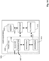
- Fig. 1 illustrates a simplified block diagram of a wireline communication system 100, according to one embodiment of the disclosure.
- the wireline communication system 100 comprises a cloud management circuit 102, a central office management (COM) circuit 104 and two distribution point unit (DPU) circuits 106a and 106b.
- the DPU circuit 106a (also the DPU circuit 106b) comprises an equipment comprising a plurality of components configured to communicate to one or more modems or transceivers over copper wire (e.g., 108a, 108b and 108c).
- each of the DPU circuits 106a and 106b is configured to couple to the modems over copper wires.
- DPU circuits may be configured to couple to one or more modems (e.g., the DPU circuit 106a). However, in other embodiments, the DPU circuits may be configured to be coupled to a single modem circuit (e.g., the DPU circuit 106b).
- the modem circuits e.g., 108a. 108b and 108b refer to any transceiver or communication device that is configured to communicate with the DPU circuit and is not to be construed as limited to a cable modem.
- the modems 108a, 108b and 108c comprises equipments that are located in a user location (e.g., customer premises equipment or CPE).
- each of the DPU circuits 106a and 106b is further configured to couple to a central office management circuit 104. In some embodiments, each of the DPU circuits 106a and 106b is configured to couple to the central office management (COM) circuit 104 over the fiber link 112.
- the DPU circuit 106 comprises a communication node located at a location closer to customer premises and enables to provide a transition between fiber networks and copper networks.
- the COM circuit 104 comprises an equipment comprising a plurality of components located at a central location of a communication system and is configured to communicate with one or more DPUs (e.g., the DPU circuits 106a and 106b).
- the COM circuit 104 may be located at a location different from the central location, for example, a communication node or at the cloud.
- the COM circuit 104 is further configured to communicate with a cloud management (CM) circuit 102 (for example, in embodiments where the COM circuit is located at a location different from the cloud).
- CM cloud management
- the COM circuit 104 is configured to coupe to the CM circuit 102 over the fiber link 114.
- the CM circuit 102 comprises an equipment comprising a plurality of components located at a head-end location (e.g., the cloud) of a communication system and is configured to couple with COM circuits (e.g., the COM circuit 104), in order to communicate with the DPUs.
- the wireline communication system 100 is shown to be coupled to only one COM circuit (i.e., the COM circuit 104).
- the CM circuit 102 may be configured to be coupled to more than one COM circuit and each of the COM circuits may be configured to be coupled to one or more DPU circuits.
- the wireline communication system 100 enables to perform virtualization of the DPU signal processing tasks. In other words, in some embodiments, the wireline communication system 100 enables to split the signal processing tasks associated with the wireline communication system 100 between the DPU circuit (e.g., the DPU circuit 106a), the COM circuit 104 and the CM circuit. In some embodiments, the task split between cloud (i.e., the CM circuit 102), CO (i.e., the COM circuit 104) and DPU/FE (i.e., the DPU circuit 106a) is selected, depending on the computation requirements associated with these tasks as well as the timing and delay and bandwidth requirements. A possible implementation of the tasks split between the cloud, the CO and the DPU/FE is illustrated in Table 1 below.
- the signal processing tasks may be split between the cloud, the CO and the DPU/FE may be split differently.
- Table 1 Signal processing tasks for wireline channel Processing task Input/output Location AD (RX) and DA (TX) conversion
- Analog signal ⁇ -> digital samples FE/DPU (required) Time domain filtering Samples (analog clock) ⁇ -> samples (band limited, lower sample rate) FE/DPU FFT (rx) and IFFT (tx) TD samples ⁇ -> FD samples FE/DPU or CO FD equalization FD samples FE/DPU or CO Echo cancellation FD samples FE/DPU or CO NEXT cancellation FD samples CO or Cloud FEXT precoding (ds) and FEXT equalization (us) FD samples CO or Cloud QAM demodulation FD samples ⁇ -> LLR (rx) and hard decision bits (tx and rx) CO or Cloud Inner FEC decoding LLR values (rx) ⁇ -> Hard decision bits CO or cloud
- the DPU circuit 106a is configured to receive a first upstream data signal 113a associated with the modem circuit 108a over the copper line 110a. Further, the DPU circuit 106a is configured to receive a second upstream data signal 115a associated with the modem circuit 108b over the copper line 110b. Upon receiving the upstream data signals 113a and 115a, in some embodiments, the DPU circuit 106a is further configured to provide the first upstream data signal 113a and the second upstream data signal 115a, in digital domain or analog domain to the COM circuit 104 over the fiber link 112. In the embodiments described throughout the disclosure, the term digital domain refers to digital signals comprising time domain samples or frequency domain samples.
- analog domain refers to analog signals.
- the digital signals and the analog signals described throughout the disclosure are different from data packets (e.g., ethernet packets).
- the DPU circuit 106a is configured to receive the first upstream data signal 113a and the second upstream data signal 115a in analog domain (e.g., as analog signals) from the respective modem circuits.
- the DPU circuit 106a is further configured to perform one or more of the signal processing operations comprising optical modulation, analog to digital conversion (A/D conversion), time domain (TD) filtering, fast Fourier transform (FFT), frequency domain (FD) equalization, on the first upstream data signal 113a and the second upstream data signal 115a, prior to providing the first upstream data signal 113a and the second upstream data signal 115a to the COM circuit 104.
- the DPU circuit 106a is further configured to perform one or more of the signal processing operations comprising optical modulation, analog to digital conversion (A/D conversion), time domain (TD) filtering, fast Fourier transform (FFT), frequency domain (FD) equalization, on the first upstream data signal 113a and the second upstream data signal 115a, prior to providing the first upstream data signal 113a and the second upstream data signal 115a to the COM circuit 104.
- A/D conversion analog to digital conversion
- TD time domain
- FFT fast Fourier transform
- FD frequency domain
- optical modulation comprises modulating the upstream data signal in analog domain on a particular fiber wavelength
- the A/D conversion comprises converting the analog signal into digital TD samples
- TD filtering comprises generating bandlimited lower sample rate TD samples.
- FFT operation comprises converting the TD samples to FD samples and FD equalization comprises quantizing the FD samples.
- the DPU circuit 106a may be configured to perform analog to digital conversion and time domain (TD) filtering of the first upstream data signal 113a (thereby generating TD samples), prior to providing the first upstream data signal 113a to the COM circuit 104.
- TD time domain
- the DPU circuit 106a may be configured to perform analog to digital conversion, time domain (TD) filtering, fast Fourier transform (FFT) and frequency domain (FD) equalization of the first upstream data signal 113a (thereby generating FD samples), prior to providing the first upstream data signal 113a to the COM circuit 104.
- TD time domain
- FFT fast Fourier transform
- FD frequency domain
- the DPU circuit 106a is further configured to provide a first downstream data signal 113b to the modem circuit 108a over the copper line 110a and provide a second downstream data signal 115b to the modem circuit 108b over the copper line 110b.
- the DPU circuit 106a is configured to provide the first downstream data signal 113b and the second downstream data signal 115b to the respective modem circuits in analog domain (e.g., as analog signals).
- the DPU circuit 106a is configured to receive the first downstream data signal 113b and the second downstream data signal 115b, in digital domain or analog domain, from the COM circuit 104.
- the DPU circuit 106a Upon receiving the first downstream data signal 113b and the second downstream data signal 115b from the COM circuit 104, in some embodiments, the DPU circuit 106a is configured to perform one or more of the signal processing operations comprising frequency domain (FD) equalization, inverse fast Fourier transform (IFFT), time domain (TD) filtering, digital to analog (D/A) conversion and optical demodulation, on the first downstream data signal 113b and the second downstream data signal 115b, prior to providing the first downstream data signal 113b and the second downstream data signal 115b to the respective modem circuits.
- FD frequency domain
- IFFT inverse fast Fourier transform
- TD time domain
- D/A digital to analog
- the DPU circuit 106a may be configured to perform TD filtering and D/A conversion on the first downstream data signal 113b (thereby generating an analog signal), prior to providing the first downstream data signal to the modem circuit 108a.
- the DPU circuit 106a may be configured to perform IFFT, TD filtering and D/A conversion on the first downstream data signal 113b (thereby generating an analog signal), prior to providing the first downstream data signal to the modem circuit 108a.
- the IFFT operation comprises converting the FD samples to TD samples.
- the DPU circuit 106a may be configured to perform optical demodulation, prior to providing the first downstream data signal to the modem circuit 108a.
- a downstream data signal interferes with an upstream data signal associated with the same line, causing echo.
- the first downstream data signal 113b may interfere with the first upstream data signal 113a on the same copper line 110a, thereby causing an echo in the first upstream data signal 113a, which needs to be cancelled.
- the DPU circuit 106a may be configured to perform echo cancellation based on the first upstream data signal 113a and the first downstream data signal 113b. Further, the DPU circuit 106a may be configured to perform echo cancellation on each line associated with the DPU circuit 106a.
- a downstream data signal associated with one line of the DPU circuit 106a may interfere with the upstream data signal of another line associated with the DPU circuit 106a causing near end crosstalk (NEXT) and far end crosstalk (FEXT).
- the first downstream data signal 113b may interfere with the second upstream data signal 115a on the copper line 110b, thereby causing NEXT and FEXT.
- the DPU circuit 106a may be further configured to perform FEXT and NEXT cancellation based on the second upstream data signal 115a and the first downstream data signal 113b.
- the second downstream data signal 115b may interfere with the first upstream data signal 113a on the copper line 110a, thereby causing near end crosstalk (NEXT) and far end crosstalk (FEXT).
- the DPU circuit 106a may be further configured to perform NEXT and FEXT cancellation based on the second upstream data signal 115a and the first downstream data signal 113b.
- DPU circuit 106a is configured to perform the crosstalk cancellation (i.e., the NEXT/FEXT/echo) in time domain or in frequency domain.
- the DPU circuits associated with the wireline communication system 100 may be configured to establish a timing reference within the DPU circuit, which in turn enables to adjust a timing associated with both the upstream data signals and the downstream data signals associated with the DPU circuit.
- the timing reference within the DPU circuits enables to establish a timing alignment between different DPU circuits that may have mutual crosstalk. In some embodiments, this precise timing reference is maintained during steady state operation (showtime) of these DPUs/FEs, which may require corrections/tuning of the timing also during showtime.
- the DPU circuit 106b is configured to receive a third upstream data signal 117a associated with the modem circuit 108c over the copper line 110c. Upon receiving the upstream data signal 117a, in some embodiments, the DPU circuit 106b is further configured to provide the third upstream data signal 117a, in digital domain or analog domain to the COM circuit 104 over the fiber link 112. In some embodiments, the DPU circuit 106b is configured to receive the third upstream data signal 117a in analog domain (e.g., as analog signals) from the modem circuit 108c.
- analog domain e.g., as analog signals
- the DPU circuit 106b is further configured to perform one or more of the signal processing operations comprising analog to digital conversion, time domain (TD) filtering, fast Fourier transform (FFT), frequency domain (FD) equalization and optical modulation, based on the third upstream data signal 117a, prior to providing the third upstream data signal 117a to the COM circuit 104.
- TD time domain
- FFT fast Fourier transform
- FD frequency domain
- the DPU circuit 106b is further configured to provide a third downstream data signal 117b to the modem circuit 108c over the copper line 110c. In some embodiments, the DPU circuit 106b is configured to provide the third downstream data signal 117b to the modem circuit 108c in analog domain (e.g., as analog signal). In some embodiments, the DPU circuit 106b is configured to receive the third downstream data signal 117b in digital domain or analog domain, from the COM circuit 104.
- the DPU circuit 106b Upon receiving the third downstream data signal 117b, in some embodiments, the DPU circuit 106b is further configured to perform one or more of the signal processing operations comprising frequency domain (FD) equalization, inverse fast fourier transform (IFFT), time domain (TD) filtering, digital to analog (D/A) conversion and optical demodulation, on the third downstream data signal 117b, prior to providing the third downstream data signal 117b to the modem circuit 108c. In some embodiments, the DPU circuit 106b is further configured to perform echo cancellation associated with the copper line 110c. In some embodiments, although not mentioned explicitly, all DPU circuits (e.g., the DPU circuit 106a and the DPU circuit 106b) associated with the wireline communication system 100 share the same features.
- FD frequency domain
- IFFT inverse fast fourier transform
- TD time domain
- D/A digital to analog
- optical demodulation optical demodulation
- the COM circuit 104 is configured to receive the first upstream data signal 113a and the second upstream data signal 115a from the DPU circuit 106a, in digital domain or analog domain. In some embodiments, the COM circuit is further configured to receive the third upstream data signal 117a from the DPU circuit 106b, in digital domain or analog domain.
- the COM circuit 104 upon receiving the upstream data signals from the DPU circuits, is further configured to perform one or more of the signal processing operations comprising analog to digital (A/D) conversion, time domain (TD) filtering, fast Fourier transform (FFT), frequency domain (FD) equalization, quadrature amplitude modulation (QAM) demodulation, constellation shaping, inner forward error correction (FEC) decoding, outer FEC decoding and data encapsulation, on the received upstream data signals.
- the COM circuit 104 is further configured to provide the received upstream signals to the CM circuits, after performing the one or more of the signal processing tasks above. However, in other embodiments, the COM circuit 104 may be configured process the upstream data signals and convey the received upstream data signals to the CM circuit 102, without performing any signal processing tasks.
- the COM circuit 104 is further configured to provide the first downstream data signal 113b and the second downstream data signal 115b to the DPU circuit 106a over the fiber link 112. In some embodiments, the COM circuit 104 is further configured to provide the third downstream data signal 117b to the DPU circuit 106b over the fiber link 112. In some embodiments, the COM circuit 104 is configured to provide the downstream data signals to the respective DPU circuits in analog domain or digital domain. In some embodiments, the COM circuit 104 is configured to receive the downstream data signals from the cloud management (CM) circuit 102. In some embodiments, the COM circuit 104 is configured to receive the downstream data signals from the cloud management (CM) circuit 102 in digital domain or analog domain or as data packets.
- CM cloud management
- CM cloud management
- the COM circuit 104 is further configured to perform one or more of the signal processing operations comprising data de-capsulation, inner forward error correction (FEC) encoding, outer FEC encoding, constellation shaping, quadrature amplitude modulation (QAM) modulation, crosstalk cancellation, frequency domain (FD) equalization, inverse fast Fourier transform (IFFT), time domain (TD) filtering, digital to analog (D/A) conversion, on the downstream data signals, in order to provide the downstream data signals to the respective DPU circuits in analog domain or digital domain.
- FEC inner forward error correction
- QAM quadrature amplitude modulation
- FD frequency domain
- IFFT inverse fast Fourier transform
- TD time domain
- D/A digital to analog
- the COM circuit 104 is further configured to perform crosstalk (NEXT/FEXT/echo) cancellation between different DPU circuits or among different lines associated with a select DPU circuit, based on processing the upstream data signals and the downstream data signals.
- the COM circuit 104 is configured to perform the crosstalk cancellation in digital domain (e.g., using TD samples or FD samples). For example, in the upstream direction, if the COM circuit 104 receives the upstream data signals in analog domain, the COM circuit 104 may be configured to perform A/D conversion and TD filtering, in order to perform cross talk cancellation using TD samples.
- the COM circuit 104 may be further configured to perform FFT on the TD samples to generate FD samples and FD equalization, in order to perform crosstalk cancellation in FD domain. However, in some embodiments, if the COM circuit 104 receives upstream data signals as FD samples, the COM circuit 104 can perform crosstalk cancellation without any further signal processing. In some embodiments, the COM circuit 104 may be further configured to provide the FD samples to the CM circuit 102 for further processing.
- the COM circuit 104 may be further configured to perform one or more of the signal processing operations on the FD samples comprising quadrature amplitude modulation (QAM) demodulation, constellation shaping, inner forward error correction (FEC) decoding, outer FEC decoding and data encapsulation, in order to generate layer 2 data packets.
- QAM quadrature amplitude modulation
- FEC forward error correction
- the COM circuit 104 is further configured to provide the layer 2 data packets to the CM circuit 102.
- the COM circuit 104 may be configured to perform data de-capsulation, outer FEC encoding, constellation shaping, inner forward error correction (FEC) encoding, quadrature amplitude modulation (QAM) modulation and frequency domain (FD) equalization, in order to perform cross talk cancellation using FD samples.
- the COM circuit 104 may be further configured to perform IFFT on the FD samples to generate TD samples and TD filtering, in order to perform crosstalk cancellation in TD domain.
- the COM circuit 104 may be configured to perform crosstalk cancellation directly, without performing any further signal processing operations.
- the COM circuit 104 may be configured provide the FD samples directly to the respective DPU circuits over the fiber link 112.
- the COM circuit 104 may be further configured to perform one or more signal processing tasks comprising IFFT, TD filtering and D/A conversion on the FD samples, in order to provide the downstream data signals to the respective DPU circuits as TD samples or in analog domain.
- the CM circuit 102 is configured to receive the first upstream data signal 113a and the second upstream data signal 115a from the COM circuit 104 over the fiber link 114. In some embodiments, the CM circuit 102 is further configured to receive the third upstream data signal 117a from the COM circuit 104. In some embodiments, the CM circuit 102 is configured to receive the upstream data signals as layer 2 data packets from the COM circuit 104. However, in other embodiments, the CM circuit 102 is configured to receive the upstream data signals in digital domain or in analog domain.
- the CM circuit 102 is further configured to perform one or more of the signal processing operations comprising analog to digital (A/D) conversion, time domain (TD) filtering, fast Fourier transform (FFT), frequency domain (FD) equalization, quadrature amplitude modulation (QAM) demodulation, constellation shaping, inner forward error correction (FEC) decoding, outer FEC decoding and data encapsulation, on the received upstream data signals, when the upstream data signals are received in analog domain or digital domain.
- A/D analog to digital
- TD time domain
- FFT fast Fourier transform
- FD frequency domain
- QAM quadrature amplitude modulation
- constellation shaping constellation shaping
- FEC inner forward error correction
- FEC outer FEC decoding
- data encapsulation data encapsulation
- the CM circuit 102 is further configured to provide the first downstream data signal 113b and the second downstream data signal 115b to the COM circuit 104 over the fiber link 114. In some embodiments, the CM circuit 102 is further configured to provide the third downstream data signal 117b to the COM circuit 104 over the fiber link 114. In some embodiments, the CM circuit 102 may be configured to provide the downstream data signals to the COM circuit 104 as layer 2 data packets. However, in other embodiments, the CM circuit 102 may be configured to provide the downstream data signals to the COM circuit 104 in analog domain or digital domain.
- the CM circuit 102 is further configured to perform one or more of the signal processing operations comprising data de-capsulation, inner forward error correction (FEC) encoding, outer FEC encoding, constellation shaping, quadrature amplitude modulation (QAM) modulation, frequency domain (FD) equalization, inverse fast Fourier transform (IFFT), time domain (TD) filtering, digital to analog (D/A) conversion, on the downstream data signals, in order to provide the downstream data signals to the COM circuit 104 in digital domain or analog domain.
- FEC inner forward error correction
- QAM quadrature amplitude modulation
- FD frequency domain
- IFFT inverse fast Fourier transform
- TD time domain
- D/A digital to analog
- the CM circuit 102 is further configured to perform crosstalk (NEXT/FEXT/echo) cancellation between different DPU circuits or among different lines associated with a select DPU circuit, based on processing the upstream data signals and the downstream data signals.
- the CM circuit 102 is configured to perform the crosstalk cancellation in digital domain (e.g., using TD samples or FD samples). Therefore, in such embodiments, the CM circuit 102 may be configured to receive the upstream data signals from the COM circuit 104 in analog domain or digital domain, and not as layer 2 data packets.
- the CM circuit 102 in the upstream direction, if the CM circuit 104 receives the upstream data signals in analog domain, the CM circuit 102 may be configured to perform A/D conversion and TD filtering, in order to perform cross talk cancellation using TD samples. In some embodiments, the CM circuit 102 may be further configured to perform FFT on the TD samples to generate FD samples and also perform FD equalization, in order to perform crosstalk cancellation in FD domain. However, in some embodiments, if the CM circuit 102 receives upstream data signals as FD samples, the CM circuit 102 can perform crosstalk cancellation without any further signal processing.
- the CM circuit 102 may be further configured to perform one or more of the signal processing operations on the FD samples comprising quadrature amplitude modulation (QAM) demodulation, constellation shaping, inner forward error correction (FEC) decoding, outer FEC decoding and data encapsulation, in order to generate layer 2 data packets.
- QAM quadrature amplitude modulation
- FEC forward error correction
- the COM circuit 104 may be configured to perform data de-capsulation, outer FEC encoding, constellation shaping, inner forward error correction (FEC) encoding, quadrature amplitude modulation (QAM) modulation and frequency domain (FD) equalization, in order to perform cross talk cancellation using FD samples.
- the CM circuit 102 may be further configured to perform IFFT on the FD samples to generate TD samples and also perform TD filtering, in order to perform crosstalk cancellation in TD domain.
- the CM circuit 102 may be configured provide the FD samples directly to the COM circuit 104 over the fiber link 114.
- the CM circuit 102 may be further configured to perform one or more signal processing tasks comprising IFFT, TD filtering and D/A conversion on the FD samples, in order to provide the downstream data signals as TD samples or in analog domain to the COM circuit 104.
- the crosstalk cancellation within the DPU circuits 106a and 106b, the COM circuit 104 and the CM circuit 102 is established based on using predefined cancellation matrices.
- the predefined cancellation matrices comprise a precoder matrix P (k) of size LxL configured to precompensate/precode the downstream data signal, in order to cancel the downstream FEXT.
- the predefined cancellation matrices further comprise an Equalizer matrix G (k) of size LxL to cancel upstream FEXT in the upstream data signal.
- the predefined cancellation matrices comprise a NEXT canceler matrix G ec (k) of size LxL configured to cancel the NEXT/echo caused by the downstream data signal.
- G ec (k) a NEXT canceler matrix of size LxL configured to cancel the NEXT/echo caused by the downstream data signal.
- the downstream data signal u ds (k) is multiplied by the precoder matrix P (k) to form the precompensated/precoded downstream signal x ds (k) as given below:
- x ds k P k u ds k
- the equation (1) is defined as a predefined far end crosstalk (FEXT) cancellation relation.
- FEXT far end crosstalk
- generating the precompensated/precoded downstream signal x ds (k) enables to reduce the downstream FEXT.
- the equation (2) is defined as a predefined near end crosstalk (NEXT) cancellation relation.
- y us (k) comprises the upstream data signal prior to NEXT/FEXT cancellation
- û us (k) is the upstream data signal after NEXT/FEXT cancellation
- u ds (k) is the downstream data signal (not precoded).
- the CM circuit 102, the COM circuit 104 and the DPU circuits may be configured to update the cancellation matrices P (k) , G (k) and G ec (k) to be utilized to perform the crosstalk cancellation.
- the cancellation matrices P (k) , G (k) and G ec (k) may be updated at the cloud (i.e., the CM circuit 102) and the resulting matrices are transmitted back to the COM circuit 104 or the DPU circuits.
- the update of the canceller matrices P (k) , G (k) and G ec (k) are performed at a much lower rate than the crosstalk cancellation operation itself.
- dedicated training symbols e.g., sync symbols are transmitted once per superframe for each direction (i.e., as part of the upstream data signal and the downstream data signal), while each superframe consists of hundreds of symbols (e.g., 288 symbols).
- Performing one matrix update per L superframes requires another 6.1 Mbyte/(8 x 6ms) gives roughly 1 Gbit/s for the coefficient update.
- a local coefficient update at the COM circuit or the DPU circuits has the advantage of reduced bandwidth on the data connection (i.e., the fiber link 114) to the cloud (1 Gbit/s+512 Mbit/s) while the coefficient update in the cloud (i.e., the CM circuit 102) comes with the advantage of more flexibility to perform changes of the coefficient update algorithms. Therefore, in the embodiments described herein, both methods may be supported and it is possible to switch between CO-based coefficient update and cloud-based coefficient update, depending on the update algorithm to be used. Different algorithms may be used for initial line training and for showtime updates.
- the bandwidth of the fiber link 112 between the COM circuit 104 and the DPU circuits 106a and 106b is a critical resource, because high bandwidth fiber links require expensive components and such components have a high power consumption.
- the DPU circuits 106a and 106b are configured to compress the upstream data signals, prior to providing the respective upstream data signals to the COM circuit 104 over the fiber link 112.
- the COM circuit 104 is also configured to compress the downstream data signals, prior to providing the downstream data signals to the DPU circuits 106a and 106b over the fiber link 112.
- the COM circuit 102 may also be configured to compress the upstream data signals, prior to providing the upstream data signals to the CM circuit 102 over the fiber link 114. Furthermore, in some embodiments, the CM circuit 102 may also be configured to compress the downstream data signals, prior to providing the downstream data signals to the COM circuit 104 over the fiber link 114.
- the signals may be compressed based on a signal decomposition method.
- the signal decomposition comprises decomposing the signal into two components where one of the components can be described with the QAM modulator function.
- the COM circuit 104 may be configured to compress the precoded downstream signal x ds (k) , prior to providing the precoded downstream signal x ds (k) over the fiber link 112.
- the signal decomposition method is applicable to any downstream data signal or upstream data signal.
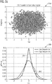
- the COM circuit 104 in order to compress the precoded downstream signal x ds (k) , is configured to decompose the DS precoded output into a set of 256-QAM constellation points (as shown in 230 in Fig. 2b ) and a random DS precoder compensation signal (as shown in 250 in Fig. 2c ).
- the precoder output signal x ds (k) consists of two signal components, the per-line QAM modulated signal u ds (k) (as shown in 240 in Fig. 2b ) as well as the pre-compensation signal, which is x ds (k) - u ds (k) (as shown in 260 in Fig.
- the pre-compensation signal x ds (k) - u ds (k) follows a Gaussian distribution at higher frequencies (as shown in 262 in Fig. 2c ) and an even sharper distribution at lower frequencies (as shown in 264 in Fig. 2c ).
- the pre-compensation signal can be compressed efficiently, using lossy nonlinear quantization.
- Both signal components can be packed into a format of b (k) bits/carrier for the QAM signal and b xtalk (k) bits/carrier and component (real/imaginary) for the pre-compensation signal.
- the signal decomposition method is implemented within the COM circuit 104. However, in other embodiments, the signal decomposition method may be implemented within the DPU circuits or the cloud, in order to compress the downstream data signals or the upstream data signals associated therewith.
- the signals may be compressed based on nonlinear quantization.
- nonlinear quantization can take advantage of any signal which doesn't follow a uniform distribution, e.g., Gaussian signals by adjusting the quantization thresholds such that the quantization error is reduced.
- the quantization method utilized comprises Lloyd-Max method, where the decision thresholds as well as the signal levels corresponding to each quantized level are iteratively optimized.
- other quantization techniques may be utilized.
- a simplified approach which achieves a similar result uses a nonlinear compressor function in advance to a uniform quantization, as shown in Fig. 3a .
- the nonlinear function can be approximated with a piece-wise linear function. Examples for such functions are the tanh function, which is the optimal compressor function for Gaussian signals or the logarithmic function, which gives a mantissa-exponent result (as it is used for speech compression).
- Nonlinear quantization on a Gaussian signal can achieve SNR gains around 3dB, depending on the selected saturation threshold.
- Fig. 3b illustrates a method for decompression of the compressed signals.
- the signal compression based on nonlinear quantization may be implemented within the DPU circuits or the COM circuit 104 or the cloud (i.e., the CM circuit 102), in order to compress the downstream data signals or the upstream data signals associated therewith.
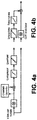
- FIG. 4a Another alternate approach uses a combination of the signal decomposition and nonlinear quantization, as shown in Fig. 4a .
- the advantage of the combined approach is that the compressed data rate scales with the actual bandwidth of the link according to the constellation size used as well as with the signal power of the residual signal.
- Fig. 4b illustrates a method to decompress the compressed signals. In cases with high bit allocation on many carriers and for high crosstalk cases, however, nonlinear quantization of the full signal, gives a higher compression rate.
- Discontinuous operation is a method to discontinue data transmission on the copper link for short periods of time in case that the data traffic required on a line is less than the available physical layer data rate. In such embodiments, crosstalk cancellation is reconfigured accordingly. In some embodiments, discontinuous operation can help to reduce bandwidth on the fiber link 112 (and the fiber link 114, in some embodiments), because for the discontinued transmission time on a line (i.e., the copper line), no data exchange between the COM circuit 104 and DPU circuits is required.
- DO can help to connect more DPUs and perform a certain virtual oversubscription of the fiber.
- dynamic resource allocation must be coordinated for the fiber and the copper links to ensure that the fiber bandwidth is available for the symbol positions which carry data.
- the COM circuit 104 is configured to schedule downstream data transmission on the fiber link 112 according to the discontinuous operation schedule on the copper lines.
- the data is processed (e.g., modulation, crosstalk cancellation) at the CO (e.g., the COM circuit 104) and then packed into data frames that supply multiple FE-CPE lines as shown in 510 in Fig. 5a .
- Fig. 5a gives an example for 3 FE-CPE lines in which data symbols are packed into data blocks, each block per FE-CPE line to be transmitted over the fiber.
- Each fiber link converts that to the corresponding DMT/OFDM signals on the copper lines.
- the COM circuit 104 is further configured to synchronize the timing of the DMT symbols on the copper lines in the way that it matches the crosstalk cancellation done previously at the CO side.
- the COM circuit 104 is further configured to arrange the data blocks for transmission over the fiber link in a way that reduces delay at the FE (or the DPU) side.
- the arrangement in 520 in Fig. 5a may result in bigger delays and requires bigger buffers at the FE side.
- An alternative implementation is shown in Fig. 5b , where the data packets of different FE-CPE lines are interleaved on the fiber.
- interleaving the data packets on fiber enables to reduce the delay at the FE side.
- the transmit time allocation on the copper line can be done such that crosstalk between different transmissions is reduced, as shown in Fig. 5b .
- Fig. 5b For example, as shown in Fig.
- the COM circuit 104 may be configured to allocate the transit time of the different copper lines in a way that there is lesser overlap between the data packets on different copper lines.
- the dynamic resource allocation may limit the copper link data rates accordingly.
- DRA engine may be part of the COM circuit 104 or in the CM circuit 102.
- the delays caused by the fiber link have to be compensated, in order to perform efficient crosstalk cancellation.
- the delay caused by the fiber is compensated based on utilizing buffers of sufficient size and appropriate timing settings between the CPE (i.e., the modem circuit) and the DPU, in order to cancel near-end crosstalk.
- a fiber delay of more than 1 DPU symbol is illustrated. In some embodiments, this delay results in the requirement to keep 3 additional DS symbols in memory (at the DPU) to cancel NEXT and echo into the corresponding US symbol.
- this timing is determined by the required timing at the CPE (i.e., the modem), which should allow echo cancellation.
- the upstream data symbols and downstream data signals should not be shifted in time by more than the selected cyclic extension. Further, in some embodiments, this CPE timing should be aligned in all lines subject for mutual crosstalk. As the delays in the fiber towards different DPUs/FEs may be different, the delay differences between different downstream symbols have to be compensated. Therefore, in some embodiments, the CM circuit 102 or the COM circuit 104 is further configured to compensate the delay differences between the downstream symbols associated with different DPU lines. In some embodiments, the CM circuit 102 or the COM circuit 104 is further configured to compensate the delay differences between the upstream symbols associated with different DPU lines.
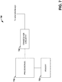
- Fig. 7 illustrates a simplified block diagram of an apparatus 700 for use in a distribution point unit (DPU) circuit associated with a wireline communication system, according to various embodiments described herein.
- the DPU circuit comprises one or more lines configured to be coupled respectively to one or more modem circuits associated therewith.
- the DPU circuit is further configured to couple to a central office management (COM) circuit over fiber.
- the apparatus 700 could be included within the DPU circuit 106a or the DPU circuit 106b in Fig. 1 . The apparatus 700 is explained herein with reference to the DPU circuit 106a of Fig. 1 .
- the apparatus 700 can be explained with reference to any DPU circuits (e.g., the DPU circuit 106b in Fig. 1 ).
- the apparatus 700 includes a processing circuit 710, a transceiver circuit 720 (which can facilitate communication of data via one or more networks in some aspects) and a memory circuit 730 (which can comprise any of a variety of storage mediums and can store instructions and/or data associated with at least one of the processor 710 or transceiver circuitry 720).
- the transceiver circuit 720 may include, inter alia, down-mixers, filters, and A/D converters to convert the high frequency upstream communication to digital data, such as baseband data for example.
- the transceiver circuit 720 may include, inter alia, up-mixers, filters, and D/A converters to convert digital data, such as baseband data for example, to high frequency downstream communication.
- the transceiver circuitry 720 passes the digital data to the processing circuit 710. However, in other embodiments, the A/D conversion and the D/A conversion may take place within the processing circuit 710. In some embodiments, the transceiver circuit 720 can comprise a receiver circuit and a transmitter circuit. In some embodiments, the processing circuit 710 can include one or more processors. In some embodiments, the one or more processors can be integrated on a single chip. However, in other embodiments, the one or more processors can be embedded on different chips. In some embodiments, the memory circuit 730 comprises a computer readable storage device that includes instructions to be executed by the processor 710.
- the memory circuit 730 can be an independent circuit and in other embodiments, the memory circuit 730 can be integrated on chip with the processor 710. Alternately, in other embodiments, the instructions to be executed by the processor 710 can be stored on a non-transitory storage medium like ROM, flash drive etc., and can be downloaded to the memory circuit 730 for execution. In some embodiments, the memory circuit 730 can comprise one or more memory circuits. In some embodiments, the one or more memory circuits can be integrated on a single chip. However, in other embodiments, the one or more memory circuits can be embedded on different chips. As described in greater detail below, apparatus 700 enables to virtualize some of the signal processing tasks associated with the DPU circuits.
- the processing circuit 710 is configured to receive, via the transceiver circuit 720, one or more upstream data signals (e.g., the first upstream data signal 113a and the second upstream data signal 115a) associated with one or more modem circuits (e.g., the modem circuit 108a and the modem circuit 108b) respectively coupled to one or more lines (e.g., the copper line 110a and the copper line 110b) associated with the processing circuit 710.
- the processing circuit 710 is configured to receive the one or more upstream data signals in analog domain (e.g., as analog signals) from the respective modem circuits.
- the processing circuit 710 Upon receiving the upstream data signals, in some embodiments, the processing circuit 710 is further configured to provide, via the transceiver circuit 720, the one or more upstream data signals in digital domain or analog domain to a COM circuit (e.g., the COM circuit 104 in Fig. 1 ) over a fiber link (e.g., the fiber link 112).
- the DPU circuit 106a is further configured to perform one or more of the signal processing operations comprising optical modulation, analog to digital conversion (A/D conversion), time domain (TD) filtering, fast Fourier transform (FFT), frequency domain (FD) equalization, on the upstream data signals, prior to providing the one or more upstream data signals to the COM circuit.
- the processing circuit 710 may be configured to perform analog to digital conversion and time domain (TD) filtering of the one or more upstream data signals received from the modem circuits, prior to providing the upstream data signals to the COM/CM circuit.
- TD time domain
- the processing circuit 710 may be configured to perform analog to digital conversion, time domain (TD) filtering, fast fourier transform (FFT) and frequency domain (FD) equalization of the upstream data signals received from the modem circuits, prior to providing the upstream data signals to the COM circuit.
- TD time domain
- FFT fast fourier transform
- FD frequency domain
- the processing circuit 710 is further configured to provide one or more downstream data signals (e.g., the first downstream data signal 113b and the second downstream data signal 115b), via the transceiver circuit 720, to the one or more modem circuits (e.g., the modem circuit 108a and the modem circuit 108b) respectively coupled to one or more lines (e.g., the copper line 110a and the copper line 110b) associated with the processing circuit 710.
- the processing circuit 710 is configured to provide the one or more downstream data signals to the respective modem circuits in analog domain (e.g., as analog signals).
- the processing circuit 710 is configured to receive, via the transceiver circuit 720, the one or more downstream data signals, in digital domain or analog domain, from the COM circuit. Upon receiving the one or more downstream data signals, in some embodiments, the processing circuit 710 is further configured to perform one or more of the signal processing operations comprising frequency domain (FD) equalization, inverse fast Fourier transform (IFFT), time domain (TD) filtering, digital to analog (D/A) conversion and optical demodulation, on the one or more downstream data signals, prior to providing the one or more downstream data signals to the respective modem circuits.
- FD frequency domain
- IFFT inverse fast Fourier transform
- TD time domain
- D/A digital to analog
- the processing circuit 710 may be configured to perform TD filtering and D/A conversion on the one or more downstream data signals (in order to generate analog signals), prior to providing the one or more downstream data signals to the respective modem circuits.
- the processing circuit 710 may be configured to receive the one or more downstream data signals in digital domain (e.g., as FD samples) over the fiber link 112, the processing circuit 710 may be configured to perform IFFT, TD filtering and D/A conversion on the one or more downstream data signals, prior to providing the one or more downstream data signals to the respective modem circuits, as explained above with respect to Fig. 1 . Further, in some embodiments, if the processing circuit 710 is configured to receive the one or more downstream data signals in analog domain over the fiber link 112, the processing circuit 710 may be configured to perform optical demodulation on the one or more downstream data signals, prior to providing the one or more downstream data signals to the respective modem circuits.
- the processing circuit 710 is further configured to perform crosstalk cancellation, based on processing the one or more upstream data signals and the one or more downstream data signals, as explained above with respect to Fig. 1 .
- the crosstalk cancellation comprises one or more of a near end cross talk (NEXT) cancellation, far end crosstalk (FEXT) cancellation and echo cancellation.
- the processing circuit 710 is configured to perform the crosstalk cancellation based on processing the one or more upstream data signals and the one or more downstream data signals, in frequency domain (i.e., using digital FD samples).
- the processing circuit 710 may be configured to perform the crosstalk cancellation based on processing the one or more upstream data signals and the one or more downstream data signals, in time domain (i.e., using digital TD samples).
- the processing circuit 710 is further configured to establish a timing reference, to enable to adjust a timing associated with both the upstream data signals and the downstream data signals associated with the DPU circuit (e.g., the DPU circuit 106a in Fig. 1 ), in order to enable an efficient cross talk cancellation within the DPU circuit.
- the processing circuit 710 is further configured to compress the one or more upstream data signals, prior to providing the one or more upstream data signals to the COM circuit over fiber.
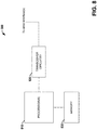
- Fig. 8 illustrates a simplified block diagram of an apparatus 800 for use in a central office management (COM) circuit associated with a wireline communication system, according to various embodiments described herein.
- the COM circuit comprises an equipment comprising a plurality of components located at a central location of a communication system and is configured to communicate with one or more DPUs.
- the COM circuit may be located at a location different from the central location, for example, a communication node or the cloud.
- the COM circuit is further configured to communicate with a cloud management (CM) circuit (in the embodiments where the COM circuit is located at a central location different from the cloud).
- CM cloud management
- the apparatus 800 could be included within the COM circuit 104 in Fig.
- the apparatus 800 includes a processing circuit 810, a transceiver circuit 820 (which can facilitate communication of data via one or more networks in some aspects) and a memory circuit 830 (which can comprise any of a variety of storage mediums and can store instructions and/or data associated with at least one of the processor 810 or transceiver circuitry 820).
- the transceiver circuit 820 may include, inter alia, down-mixers, filters, and A/D converters to convert the high frequency upstream communication to digital data, such as baseband data for example.
- the transceiver circuit 820 may include, inter alia, up-mixers, filters, and D/A converters to convert digital data, such as baseband data for example, to high frequency downstream communication.
- the transceiver circuitry 820 passes the digital data to the processing circuit 810. However, in other embodiments, the A/D conversion and the D/A conversion may take place within the processing circuit 810. In some embodiments, the transceiver circuit 820 can comprise a receiver circuit and a transmitter circuit. In some embodiments, the processing circuit 810 can include one or more processors. In some embodiments, the one or more processors can be integrated on a single chip. However, in other embodiments, the one or more processors can be embedded on different chips. In some embodiments, the memory circuit 830 comprises a computer readable storage device that includes instructions to be executed by the processor 810.
- the memory circuit 830 can be an independent circuit and in other embodiments, the memory circuit 830 can be integrated on chip with the processor 810. Alternately, in other embodiments, the instructions to be executed by the processor 810 can be stored on a non-transitory storage medium like ROM, flash drive etc., and can be downloaded to the memory circuit 830 for execution. In some embodiments, the memory circuit 830 can comprise one or more memory circuits. In some embodiments, the one or more memory circuits can be integrated on a single chip. However, in other embodiments, the one or more memory circuits can be embedded on different chips. As described in greater detail below, apparatus 800 enables to virtualize some of the signal processing tasks associated with the DPU circuits.
- the processing circuit 810 is configured to process one or more upstream data signals (e.g., the first upstream data signal 113a, the second upstream data signal 115a and the third upstream data signal 117a), received from a set of DPU circuits (e.g., the DPU circuit 106a and the DPU circuit 106b), via the transceiver circuit 820.
- the set of DPU circuits comprises one or more DPU circuits.
- the one or more upstream data signals are associated with one or more modem circuits (e.g., the modem circuits 108a, 108b and 108c in Fig. 1 ) coupled respectively to one or more lines associated with the set of DPU circuits.
- the processing circuit 810 is configured to receive the upstream data signals, in digital domain or analog domain. In some embodiments, the processing circuit 810 is further configured to process the one or more upstream data signals and perform one or more of the signal processing operations comprising analog to digital (A/D) conversion, time domain (TD) filtering, fast Fourier transform (FFT), frequency domain (FD) equalization, quadrature amplitude modulation (QAM) demodulation, constellation shaping, inner forward error correction (FEC) decoding, outer FEC decoding and data encapsulation, on the received one or more upstream data signals.
- A/D analog to digital
- TD time domain
- FFT fast Fourier transform
- FD frequency domain
- QAM quadrature amplitude modulation
- constellation shaping constellation shaping
- FEC inner forward error correction
- FEC outer FEC decoding
- data encapsulation data encapsulation
- the processing circuit 810 Upon performing the one or more of the signal processing operations on the one or more upstream data signals, in some embodiments, the processing circuit 810 is further configured to provide the one or more upstream data signals to the CM circuit. However, in other embodiments, the processing circuit 810 may be configured process the one or more upstream data signals and convey the received one or more upstream data signals to the CM circuit 102, without performing any signal processing tasks.
- the processing circuit 810 is further configured to process one or more downstream data signals (e.g., the first downstream data signal 113b, the second downstream data signal 115b and third downstream data signal 117b) to be provided to the set of DPU circuits (e.g., the DPU circuit 106a and the DPU circuit 106b), via the transceiver circuit 820, over the fiber link 112.
- the one or more downstream data signals are associated with the one or more modem circuits coupled respectively to the one or more lines associated with the set of DPU circuits.
- the processing circuit 810 is configured to receive the one or more downstream data signals from the cloud management (CM) circuit (e.g., the CM circuit 102 in Fig. 1 ).
- CM cloud management
- the processing circuit 810 is further configured to process the one or more downstream data signals and perform one or more of the signal processing operations comprising data de-capsulation, inner forward error correction (FEC) encoding, outer FEC encoding, constellation shaping, quadrature amplitude modulation (QAM) modulation, frequency domain (FD) equalization, inverse fast fourier transform (IFFT), time domain (TD) filtering, digital to analog (D/A) conversion, on the downstream data signals, prior to providing the downstream data signals to the set of DPU circuits.
- the processing circuit 810 may be configured to process the one or more downstream data signals and convey the one or more downstream data signals to the respective DPU circuits, without performing any signal processing tasks.
- the processing circuit 810 is further configured to perform crosstalk cancellation (NEXT/FEXT/echo) based on processing the one or more upstream data signals and the one or more downstream data signals.
- the processing circuit 810 is configured to perform the crosstalk cancellation in digital domain (e.g., using TD samples or FD samples). For example, in the upstream direction, if the processing circuit 810 receives the upstream data signals from the set of DPU circuits in analog domain, the processing circuit 810 may be configured to perform A/D conversion and TD filtering, on the upstream data signals in order to perform cross talk cancellation using TD samples.
- the processing circuit 810 may be further configured to perform FFT on the TD samples to generate FD samples and FD equalization, in order to perform crosstalk cancellation in FD domain. However, in some embodiments, if the processing circuit 810 receives upstream data signals as FD samples, the processing circuit 810 can perform crosstalk cancellation using the FD samples without any further signal processing. In some embodiments, the processing circuit 810 may be further configured to provide the FD samples to the CM circuit 102 for further processing.
- the processing circuit 810 may be further configured to perform one or more of the signal processing operations on the FD samples comprising quadrature amplitude modulation (QAM) demodulation, constellation shaping, inner forward error correction (FEC) decoding, outer FEC decoding and data encapsulation, in order to generate layer 2 data packets.
- the processing circuit 810 may be further configured to provide the upstream data packets to the CM circuit 102.
- the processing circuit 810 may be configured to provide the one or more upstream data signals to the CM circuit (with or without performing crosstalk cancellation) as FD samples or TD samples or in analog domain.
- the processing circuit 810 may be configured to perform data de-capsulation, outer FEC encoding, constellation shaping, inner forward error correction (FEC) encoding, quadrature amplitude modulation (QAM) modulation and frequency domain (FD) equalization, in order to perform cross talk cancellation using FD samples.
- the processing circuit 810 may be further configured to perform IFFT on the FD samples to generate TD samples and TD filtering, in order to perform crosstalk cancellation in TD domain.
- the processing circuit 810 may be configured to perform crosstalk cancellation directly on the FD samples, without performing any further signal processing operations.
- the processing circuit 810 may be configured provide the FD samples directly to the respective DPU circuits over the fiber link 112.
- the processing circuit 810 may be further configured to perform one or more signal processing tasks comprising IFFT, TD filtering and D/A conversion on the FD samples, prior to providing the FD samples to the respective DPU circuits.
- the processing circuit 810 may be configured to provide the one or more downstream signals to the DPU circuits (with or without performing crosstalk cancellation) as TD samples or FD samples or in analog domain.
- the processing circuit 810 is configured to perform the crosstalk cancellation between the one or more upstream data signals and the one or more downstream data signals based on predetermined cancellation matrices, stored within the memory circuit 830, as explained above with respect to Fig. 1 .
- performing the crosstalk cancellation comprises generating one or more precoded downstream data signals (e.g., precompensated downstream signal x ds (k) in equation (1) above), respectively based on the one or more downstream data signals, in accordance with a predefined far end crosstalk (FEXT) cancellation relation, based on the predetermined cancellation matrices, as explained above in equation (1).
- precoded downstream data signals e.g., precompensated downstream signal x ds (k) in equation (1) above
- FXT far end crosstalk
- performing the crosstalk cancellation further comprises generating one or more crosstalk compensated upstream data signals (e.g., û us (k) in equation (2) above) respectively based on the one or more upstream data signals and the one or more downstream data signals, in accordance with a predefined near end crosstalk (NEXT) cancellation relation, based on the predetermined cancellation matrices, as explained above in equation (2).
- the processing circuit 810 is further configured to update/determine the predefined cancellation matrices.
- the processing circuit 810 is configured to update/determine the predefined cancellation matrices based on receiving updated cancellation matrices from the CM circuit.
- the processing circuit 810 may be configured to update/determine predefined cancellation matrices within the processing circuit 810. In some embodiments, the processing circuit 810 is further configured to compress the downstream data signals, prior to providing the downstream data signals to the DPU circuit over fiber, as explained above with respect to Fig. 1 .
- Fig. 9 illustrates a simplified block diagram of an apparatus 900 for use in a cloud management (CM) circuit associated with a wireline communication system, according to various embodiments described herein.
- the CM circuit comprises an equipment comprising a plurality of components located at a head-end location (e.g., the cloud) of a communication system and is configured to couple with COM circuits, in order to communicate with the DPUs.
- the CM circuit may be configured to couple directly to the DPUs and may be configured to communicate directly with the DPUs.
- the apparatus 900 could be included within the CM circuit 102 in Fig. 1 .
- the apparatus 900 is explained herein with reference to the CM circuit 102 of Fig.
- the apparatus 900 includes a processing circuit 910, a transceiver circuit 920 (which can facilitate communication of data via one or more networks in some aspects) and a memory circuit 930 (which can comprise any of a variety of storage mediums and can store instructions and/or data associated with at least one of the processor 910 or transceiver circuitry 920).
- the transceiver circuit 920 may include, inter alia, down-mixers, filters, and A/D converters to convert the high frequency upstream communication to digital data, such as baseband data for example.
- the transceiver circuit 920 may include, inter alia, up-mixers, filters, and D/A converters to convert digital data, such as baseband data for example, to high frequency downstream communication.
- the transceiver circuitry 920 passes the digital data to the processing circuit 910. However, in other embodiments, the A/D conversion and the D/A conversion may take place within the processing circuit 910. In some embodiments, the transceiver circuit 920 can comprise a receiver circuit and a transmitter circuit. In some embodiments, the processing circuit 910 can include one or more processors. In some embodiments, the one or more processors can be integrated on a single chip. However, in other embodiments, the one or more processors can be embedded on different chips. In some embodiments, the memory circuit 930 comprises a computer readable storage device that includes instructions to be executed by the processor 910.
- the memory circuit 930 can be an independent circuit and in other embodiments, the memory circuit 930 can be integrated on chip with the processor 910. Alternately, in other embodiments, the instructions to be executed by the processor 910 can be stored on a non-transitory storage medium like ROM, flash drive etc., and can be downloaded to the memory circuit 930 for execution. In some embodiments, the memory circuit 930 can comprise one or more memory circuits. In some embodiments, the one or more memory circuits can be integrated on a single chip. However, in other embodiments, the one or more memory circuits can be embedded on different chips. As described in greater detail below, apparatus 900 enables to virtualize some of the signal processing tasks associated with the DPU circuits.
- the processing circuit 910 is configured to receive one or more upstream data signals (e.g., the first upstream data signal 113a, the second upstream data signal 115a and the third upstream data signal 117a) from a COM circuit (e.g., the COM circuit 104 in Fig. 1 ) via the transceiver circuit 920.
- the processing circuit 910 is configured to receive the one or more upstream data signals from the COM circuit over a fiber link (e.g., the fiber link 114 in Fig. 1 ).
- the processing circuit 910 is configured to receive the one or more upstream data signals, in digital domain or analog domain.
- the processing circuit 910 may be configured to receive the upstream data signals as layer 2 data packets from the COM circuit.
- the one or more upstream data signals are associated with one or more modem circuits (e.g., the modem circuits 108a, 108b and 108c in Fig. 1 ) coupled respectively to one or more lines (e.g., the copper lines 110a, 110b and 110c in Fig. 1 ) associated with a set of DPU circuits (e.g., the DPU circuit 106a and the DPU circuit 106b) coupled to the COM circuit.
- the set of DPU circuits comprises one or more DPU circuits.
- the processing circuit 910 is further configured to perform one or more of the signal processing operations comprising analog to digital (A/D) conversion, time domain (TD) filtering, fast fourier transform (FFT), frequency domain (FD) equalization, quadrature amplitude modulation (QAM) demodulation, constellation shaping, inner forward error correction (FEC) decoding, outer FEC decoding and data encapsulation, on the received one or more upstream data signals.
- the processing circuit 910 is configured to perform one or more of the signal processing operations on the one or more upstream data signals, in order to generate layer 2 data packets.
- the processing circuit 910 is further configured to provide one or more downstream data signals (e.g., the first downstream data signal 113b, the second downstream data signal 115b and the third downstream data signal 117b) to the COM circuit over fiber (e.g., the fiber link 114 in Fig. 1 ), via the transceiver circuit 920.
- the one or more downstream data signals are associated with the one or more modem circuits coupled respectively to the one or more lines associated with the set of DPU circuits coupled to the COM circuit.
- the one or more downstream data signals are available at the processing circuit 910 as layer 2 data packets.
- the processing circuit 910 is configured to provide the one or more downstream data signals to the COM circuit in digital domain or analog domain. However, in other embodiments, the processing circuit 910 may be configured to provide the downstream data signals to the COM circuit as layer 2 data packets.
- the processing circuit 910 is further configured to perform one or more of the signal processing operations comprising data de-capsulation, inner forward error correction (FEC) encoding, outer FEC encoding, constellation shaping, quadrature amplitude modulation (QAM) modulation, frequency domain (FD) equalization, inverse fast fourier transform (IFFT), time domain (TD) filtering, digital to analog (D/A) conversion, on the one or more downstream data signals, prior to providing the one or more downstream data signals to the COM circuit.
- FEC inner forward error correction
- QAM quadrature amplitude modulation
- FD frequency domain
- IFFT inverse fast fourier transform
- TD time domain
- the processing circuit 910 is further configured to perform crosstalk cancellation.
- the crosstalk cancellation comprises one or more of a near end cross talk (NEXT) cancellation, far end crosstalk (FEXT) cancellation and echo cancellation.
- the processing circuit 910 is configured to perform crosstalk cancellation based on processing the one or more upstream data signals and the one or more downstream data signals.
- the processing circuit 910 is configured to perform the crosstalk cancellation between the one or more upstream data signals and the one or more downstream data signals based on predefined cancellation matrices, stored within the memory circuit 930, as explained above with respect to Fig. 1 .
- the processing circuit 910 is further configured to update/determine the predefined cancellation matrices. Upon determining the predefined cancellation matrices, in some embodiments (e.g., in embodiments where crosstalk cancellation is performed at the COM circuit or the DPU circuit), the processing circuit 910 is further configured to provide the updated cancellation matrices to the COM circuit or the DPU circuits (e.g., the DPU circuit 106a in Fig. 1 ), in order to enable the COM circuit or the DPU circuits to perform crosstalk cancellation.
- the processing circuit 910 is further configured to provide the updated cancellation matrices to the COM circuit or the DPU circuits (e.g., the DPU circuit 106a in Fig. 1 ), in order to enable the COM circuit or the DPU circuits to perform crosstalk cancellation.
- the processing circuit 910 is configured to perform the crosstalk cancellation in digital domain (e.g., using TD samples or FD samples). For example, in the upstream direction, if the processing circuit 910 receives the upstream data signals in analog domain, the processing circuit 910 may be configured to perform A/D conversion and TD filtering, in order to perform cross talk cancellation using TD samples. In some embodiments, the processing circuit 910 may be further configured to perform FFT on the TD samples to generate FD samples and also perform FD equalization, in order to perform crosstalk cancellation in FD domain. However, in some embodiments, if the processing circuit 910 receives upstream data signals as FD samples, the processing circuit 910 can perform crosstalk cancellation without any further signal processing.
- the processing circuit 910 may be further configured to perform one or more of the signal processing operations on the FD samples comprising quadrature amplitude modulation (QAM) demodulation, constellation shaping, inner forward error correction (FEC) decoding, outer FEC decoding and data encapsulation, in order to generate layer 2 data packets.
- QAM quadrature amplitude modulation
- FEC forward error correction
- the processing circuit 910 may be configured to perform data de-capsulation, outer FEC encoding, constellation shaping, inner forward error correction (FEC) encoding, quadrature amplitude modulation (QAM) modulation and frequency domain (FD) equalization, on the layer 2 data packets, in order to perform cross talk cancellation using FD samples.
- the processing circuit 910 may be further configured to perform IFFT on the FD samples to generate TD samples and also perform TD filtering, in order to perform crosstalk cancellation in TD domain.
- the processing circuit 910 may be configured provide the FD samples directly to the COM circuit over the fiber link.
- the processing circuit 910 may be further configured to perform one or more signal processing tasks comprising IFFT, TD filtering and D/A conversion on the FD samples, provide the downstream data signals as TD samples or in analog domain to the COM circuit.
- Fig. 10 illustrates a flow chart of a method 1000 for a distribution point unit (DPU) circuit in a wireline communication system, according to one embodiment of the disclosure.
- the method 1000 is explained herein with reference to the apparatus 700 in Fig. 7 .
- the apparatus 700 could be included within the first DPU circuit 106a in Fig. 1 .
- one or more upstream data signals e.g., the first upstream data signal 113a and the second upstream data signal 115a in Fig. 1
- the processing circuit 710 in digital domain or analog domain
- the COM circuit e.g., the COM circuit 104 in Fig.
- the one or more upstream signals is associated with one or more lines associated with the DPU circuit which are respectively coupled to modem circuits (e.g., the modem circuit 108a and the modem circuit 108b).
- modem circuits e.g., the modem circuit 108a and the modem circuit 108b.
- one or more of the signal processing operations comprising optical modulation, analog to digital conversion, time domain (TD) filtering, fast fourier transform (FFT) and frequency domain (FD) equalization, is performed on the one or more upstream data signals, at the processing circuit 710, prior to providing the one or more upstream data signals to the COM circuit over fiber.
- the one or more upstream data signals is received at the processing circuit 710 from the respective modem circuits in analog domain (e.g., as analog signals).
- one or more downstream data signals (e.g., the first downstream data signal 113b and the second downstream data signal 115b in Fig. 1 ) is received at the processing circuit 710 from the COM circuit over fiber, in digital domain or analog domain, via the transceiver circuit 720.
- the processing circuit 710 upon receiving the one or more downstream data signals, is configured to provide the one or more downstream data signals to respective modem circuits over copper lines (e.g., the copper line 110a and the copper line 110b), in analog domain.
- one or more of the signal processing operations comprising optical demodulation, frequency domain (FD) equalization, inverse fast Fourier transform (IFFT), time domain (TD) filtering and digital to analog (D/A) conversion, are performed on the one or more downstream data signals, at the processing circuit 710, in order to provide the one or more downstream data signals to the respective modem circuits in analog domain.
- FD frequency domain
- IFFT inverse fast Fourier transform
- TD time domain
- D/A digital to analog
- crosstalk cancellation is performed at the processing circuit 710, based on processing the one or more upstream data signals and the one or more downstream data signals.
- the crosstalk cancellation comprises one or more of a near end cross talk (NEXT) cancellation, far end crosstalk (FEXT) cancellation and echo cancellation.
- the crosstalk cancellation is performed within the processing circuit 710, based on equations (1) and (2) as explained above with respect to Fig. 1 .
- instructions to execute the equations (1) and (2) are stored within the memory circuit 730.
- the crosstalk cancellation is performed at the processing circuit 710, in digital domain (e.g., using time domain (TD) samples or frequency domain (FD) samples).
- the one or more upstream data signals is compressed at the processing circuit 710, prior to providing the one or more upstream data signals to the COM circuit over fiber.
- the processing circuit 710 is configured to compress the one or more upstream data signals based on using the signal decomposition method shown in Figs. 2a , 2b and 2c above, or based on the nonlinear quantization method, as explained above with respect to Fig. 3a .
- the processing circuit 710 is further configured to establish a timing reference, to enable to adjust a timing associated with both the upstream data signals and the downstream data signals associated with the DPU circuit, in order to enable an efficient crosstalk cancellation.
- Fig. 11 illustrates a flow chart of a method 1100 for a central office management (COM) circuit in a wireline communication system, according to one embodiment of the disclosure.
- the method 1100 is explained herein with reference to the apparatus 800 in Fig. 8 .
- the apparatus 800 could be included within the COM circuit 104 in Fig. 1 .
- one or more upstream data signals e.g., the first upstream data signal 113a, the second upstream data signal 115a and the third upstream data signal 117a in Fig. 1
- a set of DPU circuits e.g., the DPU circuit 106a and the DPU circuit 106b
- fiber e.g., the fiber link 112 in Fig.
- each of one or more upstream data signals is received, at the processing circuit 810, from the respective DPU circuit in digital domain or analog domain.
- the one or more upstream data signals are associated with one or more modem circuits (e.g., the modem circuits 108a, 108b and 108c in Fig. 1 ) coupled respectively to one or more lines associated with the set of DPU circuits.
- one or more downstream data signals e.g., the first downstream data signal 113b, the second downstream data signal 115b and the third downstream data signal 117b in Fig.
- each of the one or more downstream data signals is provided to the respective DPU circuit from the processing circuit 810, in digital domain or analog domain, via the transceiver circuit 820.
- the one or more downstream data signals are associated with the one or more modem circuits coupled respectively to the one or more lines associated with the set of DPU circuits.
- the one or more downstream data signals are received at the processing circuit 810 from a CM circuit (e.g., the CM circuit 102 in Fig. 1 ) in analog domain or digital domain or as layer 2 data packets.
- one or more of the signal processing operations comprising analog to digital (A/D) conversion, time domain (TD) filtering, fast Fourier transform (FFT), frequency domain (FD) equalization, quadrature amplitude modulation (QAM) demodulation, constellation shaping, inner forward error correction (FEC) decoding, outer FEC decoding and data encapsulation, are performed on the received one or more upstream data signals, at the processing circuit 810.
- the processing circuit 810 is further configured to provide the one or more upstream data signals to the CM circuit (e.g., the CM circuit 102 in Fig. 1 ) in analog domain or digital domain or as layer 2 data packets.
- one or more of the signal processing operations comprising data de-capsulation, inner forward error correction (FEC) encoding, outer FEC encoding, constellation shaping, quadrature amplitude modulation (QAM) modulation, frequency domain (FD) equalization, inverse fast Fourier transform (IFFT), time domain (TD) filtering, digital to analog (D/A) conversion, on the one or more downstream data signals, at the processing circuit 820, prior to providing the one or more downstream data signals to the respective DPU circuits.
- the processing circuit 810 is configured to provide the one or more downstream data signals to the DPU circuits in analog domain or digital domain.
- crosstalk cancellation is performed at the processing circuit 810 based on processing the one or more of the upstream data signals respectively received from one or more lines associated with the set of DPU circuits and one or more of the downstream data signals to be provided respectively to one or more lines associated with the set of DPU circuits.
- the crosstalk cancellation comprises one or more of a near end cross talk (NEXT) cancellation, far end crosstalk (FEXT) cancellation and echo cancellation.
- the processing circuit 810 is configured to perform the crosstalk cancellation between the one or more upstream data signals and the one or more downstream data signals based on predetermined cancellation matrices.
- the crosstalk cancellation is performed within the processing circuit 810, based on equations (1) and (2) as explained above with respect to Fig. 1 .
- instructions to execute the equations (1) and (2) are stored within the memory circuit 830.
- the crosstalk cancellation is performed at the processing circuit 810, in digital domain (e.g., using time domain (TD) samples or frequency domain (FD) samples).
- the processing circuit 810 is further configured to determine/update the cancellation matrices.
- the one or more downstream data signals are compressed at the processing circuit 810, prior to providing the one or more downstream data signals to the set of DPU circuits over fiber.
- the processing circuit 810 is configured to compress the one or more downstream data signals based on using the signal decomposition method shown in Figs. 2a , 2b and 2c above, or based on the nonlinear quantization method, as explained above with respect to Fig. 3a .
- other signal compression methods different from above e.g., as shown in Fig. 4a above, are also contemplated to be within the scope of this disclosure.
- the processing circuit 810 is configured to compensate the delay differences between the downstream symbols of downstream data signals associated with different DPU lines, as explained above with respect to Fig. 6 . In some embodiments, the processing circuit 810 is configured to compensate the delay differences between the upstream symbols of upstream data signals associated with different DPU lines, as explained above with respect to Fig. 6 . In some embodiments, the processing circuit 810 is further configured to schedule a transmission of each of the downstream data signals to a respective DPU circuit, in accordance with a discontinuation operation schedule of the modem circuits configured to receive the respective downstream data signals, as explained above with respect to Fig. 5a and Fig. 5b above.
- Fig. 12 illustrates a flow chart of a method 1200 for a cloud management (CM) circuit in a wireline communication system, according to one embodiment of the disclosure.
- the method 1200 is explained herein with reference to the apparatus 900 in Fig. 9 .
- one or more upstream data signals (e.g., the first upstream data signal 113a, the second upstream data signal 115a and the third upstream data signal 117a in Fig. 1 ) is received at the processing circuit 910, from a COM circuit (e.g., the COM circuit 104 in Fig. 1 ), in analog domain or in digital domain, via the transceiver circuit 920.
- a COM circuit e.g., the COM circuit 104 in Fig. 1
- the one or more upstream data signals may be received at the processing circuit 910 as layer 2 data packets.
- the one or more upstream data signals are associated with one or more modem circuits (e.g., the modem circuits 108a, 108b and 108c in Fig. 1 ) coupled respectively to one or more lines (e.g., the copper lines 110a, 110b and 110c in Fig. 1 ) associated with a set of DPU circuits (e.g., the DPU circuit 106a and the DPU circuit 106b) coupled to the COM circuit.
- modem circuits e.g., the modem circuits 108a, 108b and 108c in Fig. 1
- lines e.g., the copper lines 110a, 110b and 110c in Fig. 1
- DPU circuits e.g., the DPU circuit 106a and the DPU circuit 106b
- one or more of the signal processing operations comprising analog to digital (A/D) conversion, TD filtering, fast Fourier transform (FFT), frequency domain (FD) equalization, quadrature amplitude modulation (QAM) demodulation, constellation shaping, inner forward error correction (FEC) decoding, outer FEC decoding and data encapsulation, is performed on the one or more upstream data signals (for example, in embodiments where the one or more upstream data signals are received in analog domain or digital domain), at the processing circuit 910, upon receiving the one or more upstream data signals.
- A/D analog to digital
- FFT fast Fourier transform
- FD frequency domain
- QAM quadrature amplitude modulation
- constellation shaping for example, in embodiments where the one or more upstream data signals are received in analog domain or digital domain
- one or more downstream data signals are provided from the processing circuit 910, in digital domain or analog domain, to the COM circuit (e.g., the COM circuit 104 in Fig. 1 ), via the transceiver circuit 920.
- the one or more downstream data signals may be provided to the processing circuit 910 as layer 2 data packets.
- the one or more downstream data signals are associated with the one or more modem circuits coupled respectively to one or more lines associated with the set of DPU circuits coupled to the COM circuit.
- one or more of the signal processing operations comprising data de-capsulation, inner forward error correction (FEC) encoding, outer FEC encoding, constellation shaping, quadrature amplitude modulation (QAM) modulation, frequency domain (FD) equalization, inverse fast Fourier transform (IFFT), time domain (TD) filtering and digital to analog (D/A) conversion, are performed on the one or more downstream data signals (for example, in embodiments where the one or more downstream data signals are provided in analog domain or digital domain), at the processing circuit 910, prior to providing the one or more downstream data signals to the COM circuit.
- FEC forward error correction
- QAM quadrature amplitude modulation
- FD frequency domain
- IFFT inverse fast Fourier transform
- TD time domain
- crosstalk cancellation is performed at the processing circuit 910, based on processing the one or more upstream data signals and the one or more downstream data signals.
- the crosstalk cancellation comprises one or more of a near end cross talk (NEXT) cancellation, far end crosstalk (FEXT) cancellation and echo cancellation.
- the processing circuit 810 configured to perform the crosstalk cancellation between the one or more upstream data signals and the one or more downstream data signals based on predetermined cancellation matrices.
- the crosstalk cancellation is performed within the processing circuit 910, based on equations (1) and (2) as explained above with respect to Fig. 1 .
- instructions to execute the equations (1) and (2) are stored within the memory circuit 930.
- the crosstalk cancellation is performed at the processing circuit 910, in digital domain (e.g., using time domain (TD) samples or frequency domain (FD) samples).
- a cancellation matrix update comprising updating/determining one or more cancellation matrices to be utilized in crosstalk cancellation is performed at the processing circuit 910, based on processing the one or more upstream data signals and the one or more downstream data signals.
- the processing circuit 910 is further configured to provide the determined cancellation matrices to the COM circuit/the DPU circuits, in order to enable the COM circuit/DPU circuits to perform crosstalk cancellation.
- Fig. 13 illustrates a functional reference model of a physical medium dependent layer (PMD) of G.fast or MGFAST Recommendation (as referenced in ITU G.9701 standard), according to various embodiments described herein.
- the interface between different DPUs may be defined at ⁇ (k, n) and ⁇ (k, n) reference points, which provide signal samples from other lines in the aim to cancel FEXT.
- signal samples from other lines and from the own transmission allow to cancel echo and NEXT caused by use of full-duplex transmission.
- signal samples associated with multiple DPUs/FEs are only available at the central point (CO or the cloud), and have to be delivered there via fiber.
- a full set of frequency domain samples in TX and RX directions shall be communicated through the fiber to the CO or the cloud, in order to enable FEXT/NEXT/echo cancellation at the CO or the cloud.
- the set of frequency domain samples corresponds to reference point Z i' of the transmitter and peer point (input of the post-canceller) of the receiver.
- any reference point below Z i' of the transmitter and, respectively, below the input of the post-canceller of the receiver can serve as well.
- Tx and Rx points after the "TDD switch control" in Fig. 13 can be used. Use of particular demarcation point is a tradeoff between complexity left at the DPU and transmission capacity required for the fiber.
- FIG. 14 illustrates a block diagram of an embodiment of device 1400 (e.g., a modem, a cable modem or gateway, etc.) related to access of a network (e.g., base station, wireless access point, femtocell access point, and so forth) that can enable and/or exploit features or aspects of the disclosed aspects.
- a network e.g., base station, wireless access point, femtocell access point, and so forth
- the device 1400 can be utilized with one or more aspects (e.g., the CM circuit 102 in Fig. 1 , the COM circuit 104 in Fig. 1 , the DPU circuits 106a and 106b in Fig. 1 , and the modem circuits 108a, 108b and 108c in Fig. 1 ) of communication networks described herein according to various aspects.
- the user device 1400 for example, comprises a digital baseband processor 1402 that can be coupled to a data store or memory 1403 and a front end 1404 (e.g., an RF front end, an acoustic front end, an optical front end, or the other like front end).
- the device 1400 further comprises one or more input/output ports 1407 configured to receive and transmit signals to and from one or more devices such as access points, access terminals, wireless ports, routers and so forth, which can operate within a radio access network or other communication network generated via a network device (not shown).
- devices such as access points, access terminals, wireless ports, routers and so forth, which can operate within a radio access network or other communication network generated via a network device (not shown).
- the device 1400 can be a radio frequency (RF) device for communicating RF signals, an acoustic device for communicating acoustic signals, an optical device for communicating optical signals, or any other signal communication device, such as a computer, a personal digital assistant, a mobile phone or smart phone, a tablet PC, a modem, a notebook, a router, a switch, a repeater, a PC, network device, base station or a like device that can operate to communicate with a network or other device according to one or more different communication protocols or standards.
- RF radio frequency
- the front end 1404 can include a communication platform, which comprises electronic components and associated circuitry that provide for processing, manipulation or shaping of the received or transmitted signals via one or more receivers or transmitters (e.g. transceivers) 1408, a mux/demux component 1412, and a mod/demod component 1414.
- the front end 1404 is coupled to the digital baseband processor 1402 and the set of input/output ports 1407.
- the front end 1404 may be configured to perform the remodulation techniques described herein to extend the frequency range of the device 1400.
- the user equipment device 1400 can comprise a phase locked loop system 1410.
- the processor 1402 can confer functionality, at least in part, to substantially any electronic component within the mobile communication device 1400, in accordance with aspects of the disclosure.
- the processor 1402 can be configured to execute, at least in part, executable instructions that cause the front end to remodulate signals to selected frequencies.
- the processor 1402 is functionally and/or communicatively coupled (e.g., through a memory bus) to memory 1403 in order to store or retrieve information necessary to operate and confer functionality, at least in part, to communication platform or front end 1404, the phase locked loop system 1410 and substantially any other operational aspects of the phase locked loop system 1410.
- the phase locked loop system 1410 includes at least one oscillator (e.g., a VCO, DCO or the like) that can be calibrated via core voltage, a coarse tuning value, signal, word or selection process.
- the processor 1402 can operate to enable the mobile communication device 1400 to process data (e.g., symbols, bits, or chips) for multiplexing/demultiplexing with the mux/demux component 1412, or modulation/demodulation via the mod/demod component 1414, such as implementing direct and inverse fast Fourier transforms, selection of modulation rates, selection of data packet formats, inter-packet times, etc.
- data e.g., symbols, bits, or chips
- Memory 1403 can store data structures (e.g., metadata), code structure(s) (e.g., modules, objects, classes, procedures, or the like) or instructions, network or device information such as policies and specifications, attachment protocols, code sequences for scrambling, spreading and pilot (e.g., reference signal(s)) transmission, frequency offsets, cell IDs, and other data for detecting and identifying various characteristics related to RF input signals, a power output or other signal components during power generation.
- data structures e.g., metadata
- code structure(s) e.g., modules, objects, classes, procedures, or the like
- instructions e.g., modules, objects, classes, procedures, or the like
- network or device information such as policies and specifications, attachment protocols, code sequences for scrambling, spreading and pilot (e.g., reference signal(s)) transmission, frequency offsets, cell IDs, and other data for detecting and identifying various characteristics related to RF input signals, a power output or other signal components during power generation.
- Examples can include subject matter such as a method, means for performing acts or blocks of the method, at least one machine-readable medium including instructions that, when performed by a machine cause the machine to perform acts of the method or of an apparatus or system for concurrent communication using multiple communication technologies according to embodiments and examples described herein.
- DSP digital signal processor
- ASIC application specific integrated circuit
- FPGA field programmable gate array
- a general-purpose processor can be a microprocessor, but, in the alternative, processor can be any conventional processor, controller, microcontroller, or state machine.
Landscapes
- Engineering & Computer Science (AREA)
- Computer Networks & Wireless Communication (AREA)
- Signal Processing (AREA)
- Physics & Mathematics (AREA)
- Electromagnetism (AREA)
- Cable Transmission Systems, Equalization Of Radio And Reduction Of Echo (AREA)
Applications Claiming Priority (2)
| Application Number | Priority Date | Filing Date | Title |
|---|---|---|---|
| US201862658278P | 2018-04-16 | 2018-04-16 | |
| US16/281,238 US10873366B2 (en) | 2018-04-16 | 2019-02-21 | Virtual distribution point architecture |
Publications (3)
| Publication Number | Publication Date |
|---|---|
| EP3557773A2 true EP3557773A2 (de) | 2019-10-23 |
| EP3557773A3 EP3557773A3 (de) | 2019-11-27 |
| EP3557773B1 EP3557773B1 (de) | 2022-09-07 |
Family
ID=65903893
Family Applications (1)
| Application Number | Title | Priority Date | Filing Date |
|---|---|---|---|
| EP19162689.4A Active EP3557773B1 (de) | 2018-04-16 | 2019-03-13 | Architektur eines virtuellen verteilungspunktes |
Country Status (2)
| Country | Link |
|---|---|
| US (1) | US10873366B2 (de) |
| EP (1) | EP3557773B1 (de) |
Families Citing this family (1)
| Publication number | Priority date | Publication date | Assignee | Title |
|---|---|---|---|---|
| WO2025019836A2 (en) * | 2023-07-19 | 2025-01-23 | Maxlinear, Inc. | Low complexity soft decision optical receiver |
Family Cites Families (37)
| Publication number | Priority date | Publication date | Assignee | Title |
|---|---|---|---|---|
| US7394752B2 (en) * | 2001-11-06 | 2008-07-01 | The Board Of Trusttees Of The Leland Stanford Junior University | Joint reduction of NEXT and FEXT in xDSL systems |
| US20080002718A1 (en) * | 2006-06-30 | 2008-01-03 | Bernard Marc R | Method and apparatus to restore default settings in an Optical Network Terminal (ONT) |
| US8978085B2 (en) * | 2006-12-28 | 2015-03-10 | General Instrument Corporation | Return data path in an HFC network |
| US8396369B1 (en) * | 2007-09-28 | 2013-03-12 | Aurora Networks, Inc. | Method and system for propagating upstream cable modem signals and RF return video control signals over the same optical network |
| US20110033189A1 (en) * | 2008-10-29 | 2011-02-10 | Calix Networks, Inc. | Return path compliance in networks |
| US8428465B2 (en) * | 2008-10-29 | 2013-04-23 | Calix, Inc. | Return path for uspstream communications originating from optical node |
| US8218419B2 (en) * | 2009-02-12 | 2012-07-10 | Alcatel Lucent | Simultaneous estimation of multiple channel coefficients using a common probing sequence |
| US8544051B1 (en) * | 2009-03-30 | 2013-09-24 | Cisco Technology, Inc. | Broadcast solution for cable IPTV |
| WO2011009593A2 (en) * | 2009-07-20 | 2011-01-27 | Lantiq Deutschland Gmbh | Method and apparatus for vectored data transmission |
| GB2474943A (en) * | 2009-10-27 | 2011-05-04 | Lantiq Deutschland Gmbh | Vectored data transmission to reduce crosstalk between connections |
| US20120051734A1 (en) * | 2010-08-24 | 2012-03-01 | General Instrument Corporation | Status monitor transponder for an optical node of a network |
| US8649686B1 (en) * | 2010-11-24 | 2014-02-11 | Applied Micro Circuits Corporation | System and method for closed-loop optical network power backoff |
| US8537655B2 (en) * | 2011-01-28 | 2013-09-17 | Alcatel Lucent | Multiplicative updating of precoder or postcoder matrices for crosstalk control in a communication system |
| WO2012104982A1 (ja) * | 2011-01-31 | 2012-08-09 | 富士通株式会社 | 光送信器および光信号送信方法 |
| US8977126B2 (en) * | 2011-04-05 | 2015-03-10 | Broadcom Corporation | Unified network management of hybrid fiber coaxial (HFC) network |
| US8848523B2 (en) * | 2011-04-05 | 2014-09-30 | Broadcom Corporation | Method for sub-rating an ethernet passive optical network (EPON) medium access control (MAC) based communication link |
| US9031409B2 (en) * | 2011-04-29 | 2015-05-12 | Arris Technology, Inc. | System and method for avoiding upstream interference in RF-over-glass network |
| US9113237B2 (en) * | 2012-02-03 | 2015-08-18 | Broadcom Corporation | Systems and methods for ethernet passive optical network over coaxial (EPOC) power saving modes |
| US8761294B2 (en) * | 2012-02-17 | 2014-06-24 | Alcatel Lucent | Methods and systems for reducing crosstalk |
| US9071358B2 (en) * | 2012-06-21 | 2015-06-30 | Qualcomm Incrorporated | Repeater fiber-coax units |
| EP2690805B1 (de) * | 2012-07-23 | 2020-05-27 | Lantiq Beteiligungs-GmbH & Co.KG | Spektrummanagement und Zeitoptimierung über mehrere Verteilungspunkte |
| KR20150067133A (ko) * | 2012-07-27 | 2015-06-17 | 어댑티브 스펙트럼 앤드 시그널 얼라인먼트, 인크. | 구리(copper)를 통한 시분할 듀플렉스 전송을 관리하는 방법들 및 관리 시스템 |
| WO2014062574A1 (en) * | 2012-10-16 | 2014-04-24 | Huawei Technologies Co., Ltd. | Data transmission coordination over digital subscriber lines |
| US10033430B2 (en) * | 2012-10-30 | 2018-07-24 | Lantiq Deutschland Gmbh | Spectrum management |
| WO2014194532A1 (zh) * | 2013-06-08 | 2014-12-11 | 华为技术有限公司 | 网络节点传输方法及其装置、系统 |
| EP3522455B1 (de) * | 2013-09-09 | 2024-10-09 | British Telecommunications public limited company | Fasernetzwerk-proxy |
| EP2852067B1 (de) | 2013-09-23 | 2016-11-16 | Alcatel Lucent | Vorrichtungen und Verfahren zur vorangegangenen und nachträglichen Kompensation von Übersprechen |
| CN108965497B (zh) * | 2013-11-13 | 2021-09-07 | 华为技术有限公司 | 接入网虚拟化的方法及代理节点 |
| US9647786B2 (en) * | 2013-12-27 | 2017-05-09 | Arris Enterprises, Inc. | Determining bitloading profiles based on sNR measurements |
| WO2015127624A1 (zh) * | 2014-02-27 | 2015-09-03 | 华为技术有限公司 | 串扰信道估计方法、矢量化控制实体及osd系统 |
| US9577756B2 (en) * | 2014-03-26 | 2017-02-21 | Arris Enterprises, Inc. | Optical beat interference detection and mitigation |
| GB2542045B (en) * | 2014-05-30 | 2020-12-23 | British Telecomm | Dynamic line management engine residing in the access network |
| US10374887B2 (en) * | 2014-08-27 | 2019-08-06 | Assia Spe, Llc | Systems, methods, and apparatuses for implementing the virtualization of access node functions |
| US9749056B2 (en) * | 2015-01-14 | 2017-08-29 | Huawei Technologies Co., Ltd | Method and system for discrete multi-tone transmission with multiple modulations |
| US20160294441A1 (en) * | 2015-03-30 | 2016-10-06 | Futurewei Technologies, Inc. | Copper-Assisted Fifth Generation (5G) Wireless Access to Indoor |
| US9991932B2 (en) * | 2016-02-29 | 2018-06-05 | Arris Enterprises Llc | MoCA network system for multiple dwelling units |
| US11411606B2 (en) * | 2016-03-24 | 2022-08-09 | Telefonaktiebolaget Lm Ericsson (Publ) | Method and system for estimating crosstalk between electrical transmission lines |
-
2019
- 2019-02-21 US US16/281,238 patent/US10873366B2/en active Active
- 2019-03-13 EP EP19162689.4A patent/EP3557773B1/de active Active
Non-Patent Citations (1)
| Title |
|---|
| None |
Also Published As
| Publication number | Publication date |
|---|---|
| US20190319668A1 (en) | 2019-10-17 |
| EP3557773B1 (de) | 2022-09-07 |
| EP3557773A3 (de) | 2019-11-27 |
| US10873366B2 (en) | 2020-12-22 |
Similar Documents
| Publication | Publication Date | Title |
|---|---|---|
| US9531491B2 (en) | Communication method, apparatus and system | |
| US9106415B2 (en) | Microwave backhaul system having a double capacity link | |
| CN103125104B (zh) | 用于操作矢量化vdsl线路组的方法 | |
| US20180262926A1 (en) | Excursion compensation in multipath communication systems with a cyclic prefix | |
| US20160294441A1 (en) | Copper-Assisted Fifth Generation (5G) Wireless Access to Indoor | |
| US9906353B2 (en) | Scheme system and method for power saving in vectored communications | |
| US20140023127A1 (en) | System and Method for Selecting Parameters for Compressing Coefficients for Nodescale Vectoring | |
| TWI622277B (zh) | 鎖定之長方調節 | |
| US11411603B2 (en) | Device for transmitting and receiving on a copper wire installed at a customer premise | |
| US10742508B2 (en) | Customer bandwidth re-distribution in point-to-multipoint access | |
| US20120026926A1 (en) | Low power mode for vectored data transmission | |
| US20140185704A1 (en) | Hitless Modulation Changes in Double Capacity Links Using Adaptive Coding Modulation (ACM) | |
| EP2286574A1 (de) | Verfahren und vorrichtung zur verringerung des feedback-overhead während der initialisierung eines übersprechvorkodierer | |
| US20150055568A1 (en) | Self-Interference Cancellation | |
| US20190273536A1 (en) | Excursion compensation in multipath communication systems with a cyclic prefix | |
| US20140153630A1 (en) | Rate-adaptive dynamic spectrum management | |
| CN113785499B (zh) | 一种节点电路及电缆调制解调器终端系统cmts电路 | |
| EP3557773B1 (de) | Architektur eines virtuellen verteilungspunktes | |
| CN102656813B (zh) | 使用带宽自适应预编码器接口的串扰控制方法和装置 | |
| US11689399B2 (en) | Apparatus, method and non-transitory, computer readable storage media for transmitting and receiving discontinuous time-frequency operation signals in a communication network | |
| Strobel | Channel Modeling and Physical Layer Optimization in Copper Line Networks | |
| EP3754860B1 (de) | Strahlformung mit geringer komplexität für ein mehrleitungskommunikationssystem | |
| Cai et al. | A novel efficient wireless fronthaul (EWF) method for the common public radio interface (CPRI) signal transmission | |
| CN110661736B (zh) | 信号处理方法及相关装置 | |
| WO2011077430A1 (en) | Dsm cross-talk cancellation technique for xdsl lines |
Legal Events
| Date | Code | Title | Description |
|---|---|---|---|
| PUAI | Public reference made under article 153(3) epc to a published international application that has entered the european phase |
Free format text: ORIGINAL CODE: 0009012 |
|
| STAA | Information on the status of an ep patent application or granted ep patent |
Free format text: STATUS: THE APPLICATION HAS BEEN PUBLISHED |
|
| AK | Designated contracting states |
Kind code of ref document: A2 Designated state(s): AL AT BE BG CH CY CZ DE DK EE ES FI FR GB GR HR HU IE IS IT LI LT LU LV MC MK MT NL NO PL PT RO RS SE SI SK SM TR |
|
| AX | Request for extension of the european patent |
Extension state: BA ME |
|
| PUAL | Search report despatched |
Free format text: ORIGINAL CODE: 0009013 |
|
| AK | Designated contracting states |
Kind code of ref document: A3 Designated state(s): AL AT BE BG CH CY CZ DE DK EE ES FI FR GB GR HR HU IE IS IT LI LT LU LV MC MK MT NL NO PL PT RO RS SE SI SK SM TR |
|
| AX | Request for extension of the european patent |
Extension state: BA ME |
|
| RIC1 | Information provided on ipc code assigned before grant |
Ipc: H04B 3/32 20060101AFI20191018BHEP |
|
| STAA | Information on the status of an ep patent application or granted ep patent |
Free format text: STATUS: REQUEST FOR EXAMINATION WAS MADE |
|
| 17P | Request for examination filed |
Effective date: 20200527 |
|
| RBV | Designated contracting states (corrected) |
Designated state(s): AL AT BE BG CH CY CZ DE DK EE ES FI FR GB GR HR HU IE IS IT LI LT LU LV MC MK MT NL NO PL PT RO RS SE SI SK SM TR |
|
| STAA | Information on the status of an ep patent application or granted ep patent |
Free format text: STATUS: EXAMINATION IS IN PROGRESS |
|
| 17Q | First examination report despatched |
Effective date: 20210225 |
|
| GRAP | Despatch of communication of intention to grant a patent |
Free format text: ORIGINAL CODE: EPIDOSNIGR1 |
|
| STAA | Information on the status of an ep patent application or granted ep patent |
Free format text: STATUS: GRANT OF PATENT IS INTENDED |
|
| INTG | Intention to grant announced |
Effective date: 20220406 |
|
| RAP1 | Party data changed (applicant data changed or rights of an application transferred) |
Owner name: MAXLINEAR ASIA SINGAPORE PRIVATE LIMITED |
|
| GRAS | Grant fee paid |
Free format text: ORIGINAL CODE: EPIDOSNIGR3 |
|
| GRAA | (expected) grant |
Free format text: ORIGINAL CODE: 0009210 |
|
| STAA | Information on the status of an ep patent application or granted ep patent |
Free format text: STATUS: THE PATENT HAS BEEN GRANTED |
|
| AK | Designated contracting states |
Kind code of ref document: B1 Designated state(s): AL AT BE BG CH CY CZ DE DK EE ES FI FR GB GR HR HU IE IS IT LI LT LU LV MC MK MT NL NO PL PT RO RS SE SI SK SM TR |
|
| REG | Reference to a national code |
Ref country code: GB Ref legal event code: FG4D |
|
| REG | Reference to a national code |
Ref country code: CH Ref legal event code: EP Ref country code: AT Ref legal event code: REF Ref document number: 1517903 Country of ref document: AT Kind code of ref document: T Effective date: 20220915 |
|
| REG | Reference to a national code |
Ref country code: IE Ref legal event code: FG4D |
|
| REG | Reference to a national code |
Ref country code: DE Ref legal event code: R096 Ref document number: 602019019137 Country of ref document: DE |
|
| REG | Reference to a national code |
Ref country code: LT Ref legal event code: MG9D |
|
| REG | Reference to a national code |
Ref country code: NL Ref legal event code: MP Effective date: 20220907 |
|
| PG25 | Lapsed in a contracting state [announced via postgrant information from national office to epo] |
Ref country code: SE Free format text: LAPSE BECAUSE OF FAILURE TO SUBMIT A TRANSLATION OF THE DESCRIPTION OR TO PAY THE FEE WITHIN THE PRESCRIBED TIME-LIMIT Effective date: 20220907 Ref country code: RS Free format text: LAPSE BECAUSE OF FAILURE TO SUBMIT A TRANSLATION OF THE DESCRIPTION OR TO PAY THE FEE WITHIN THE PRESCRIBED TIME-LIMIT Effective date: 20220907 Ref country code: NO Free format text: LAPSE BECAUSE OF FAILURE TO SUBMIT A TRANSLATION OF THE DESCRIPTION OR TO PAY THE FEE WITHIN THE PRESCRIBED TIME-LIMIT Effective date: 20221207 Ref country code: LV Free format text: LAPSE BECAUSE OF FAILURE TO SUBMIT A TRANSLATION OF THE DESCRIPTION OR TO PAY THE FEE WITHIN THE PRESCRIBED TIME-LIMIT Effective date: 20220907 Ref country code: LT Free format text: LAPSE BECAUSE OF FAILURE TO SUBMIT A TRANSLATION OF THE DESCRIPTION OR TO PAY THE FEE WITHIN THE PRESCRIBED TIME-LIMIT Effective date: 20220907 Ref country code: FI Free format text: LAPSE BECAUSE OF FAILURE TO SUBMIT A TRANSLATION OF THE DESCRIPTION OR TO PAY THE FEE WITHIN THE PRESCRIBED TIME-LIMIT Effective date: 20220907 |
|
| REG | Reference to a national code |
Ref country code: AT Ref legal event code: MK05 Ref document number: 1517903 Country of ref document: AT Kind code of ref document: T Effective date: 20220907 |
|
| PG25 | Lapsed in a contracting state [announced via postgrant information from national office to epo] |
Ref country code: HR Free format text: LAPSE BECAUSE OF FAILURE TO SUBMIT A TRANSLATION OF THE DESCRIPTION OR TO PAY THE FEE WITHIN THE PRESCRIBED TIME-LIMIT Effective date: 20220907 Ref country code: GR Free format text: LAPSE BECAUSE OF FAILURE TO SUBMIT A TRANSLATION OF THE DESCRIPTION OR TO PAY THE FEE WITHIN THE PRESCRIBED TIME-LIMIT Effective date: 20221208 |
|
| PG25 | Lapsed in a contracting state [announced via postgrant information from national office to epo] |
Ref country code: SM Free format text: LAPSE BECAUSE OF FAILURE TO SUBMIT A TRANSLATION OF THE DESCRIPTION OR TO PAY THE FEE WITHIN THE PRESCRIBED TIME-LIMIT Effective date: 20220907 Ref country code: RO Free format text: LAPSE BECAUSE OF FAILURE TO SUBMIT A TRANSLATION OF THE DESCRIPTION OR TO PAY THE FEE WITHIN THE PRESCRIBED TIME-LIMIT Effective date: 20220907 Ref country code: PT Free format text: LAPSE BECAUSE OF FAILURE TO SUBMIT A TRANSLATION OF THE DESCRIPTION OR TO PAY THE FEE WITHIN THE PRESCRIBED TIME-LIMIT Effective date: 20230109 Ref country code: ES Free format text: LAPSE BECAUSE OF FAILURE TO SUBMIT A TRANSLATION OF THE DESCRIPTION OR TO PAY THE FEE WITHIN THE PRESCRIBED TIME-LIMIT Effective date: 20220907 Ref country code: CZ Free format text: LAPSE BECAUSE OF FAILURE TO SUBMIT A TRANSLATION OF THE DESCRIPTION OR TO PAY THE FEE WITHIN THE PRESCRIBED TIME-LIMIT Effective date: 20220907 Ref country code: AT Free format text: LAPSE BECAUSE OF FAILURE TO SUBMIT A TRANSLATION OF THE DESCRIPTION OR TO PAY THE FEE WITHIN THE PRESCRIBED TIME-LIMIT Effective date: 20220907 |
|
| PG25 | Lapsed in a contracting state [announced via postgrant information from national office to epo] |
Ref country code: SK Free format text: LAPSE BECAUSE OF FAILURE TO SUBMIT A TRANSLATION OF THE DESCRIPTION OR TO PAY THE FEE WITHIN THE PRESCRIBED TIME-LIMIT Effective date: 20220907 Ref country code: PL Free format text: LAPSE BECAUSE OF FAILURE TO SUBMIT A TRANSLATION OF THE DESCRIPTION OR TO PAY THE FEE WITHIN THE PRESCRIBED TIME-LIMIT Effective date: 20220907 Ref country code: IS Free format text: LAPSE BECAUSE OF FAILURE TO SUBMIT A TRANSLATION OF THE DESCRIPTION OR TO PAY THE FEE WITHIN THE PRESCRIBED TIME-LIMIT Effective date: 20230107 Ref country code: EE Free format text: LAPSE BECAUSE OF FAILURE TO SUBMIT A TRANSLATION OF THE DESCRIPTION OR TO PAY THE FEE WITHIN THE PRESCRIBED TIME-LIMIT Effective date: 20220907 |
|
| REG | Reference to a national code |
Ref country code: DE Ref legal event code: R097 Ref document number: 602019019137 Country of ref document: DE |
|
| PG25 | Lapsed in a contracting state [announced via postgrant information from national office to epo] |
Ref country code: NL Free format text: LAPSE BECAUSE OF FAILURE TO SUBMIT A TRANSLATION OF THE DESCRIPTION OR TO PAY THE FEE WITHIN THE PRESCRIBED TIME-LIMIT Effective date: 20220907 Ref country code: AL Free format text: LAPSE BECAUSE OF FAILURE TO SUBMIT A TRANSLATION OF THE DESCRIPTION OR TO PAY THE FEE WITHIN THE PRESCRIBED TIME-LIMIT Effective date: 20220907 |
|
| P01 | Opt-out of the competence of the unified patent court (upc) registered |
Effective date: 20230601 |
|
| PLBE | No opposition filed within time limit |
Free format text: ORIGINAL CODE: 0009261 |
|
| STAA | Information on the status of an ep patent application or granted ep patent |
Free format text: STATUS: NO OPPOSITION FILED WITHIN TIME LIMIT |
|
| PG25 | Lapsed in a contracting state [announced via postgrant information from national office to epo] |
Ref country code: DK Free format text: LAPSE BECAUSE OF FAILURE TO SUBMIT A TRANSLATION OF THE DESCRIPTION OR TO PAY THE FEE WITHIN THE PRESCRIBED TIME-LIMIT Effective date: 20220907 |
|
| 26N | No opposition filed |
Effective date: 20230608 |
|
| PG25 | Lapsed in a contracting state [announced via postgrant information from national office to epo] |
Ref country code: SI Free format text: LAPSE BECAUSE OF FAILURE TO SUBMIT A TRANSLATION OF THE DESCRIPTION OR TO PAY THE FEE WITHIN THE PRESCRIBED TIME-LIMIT Effective date: 20220907 |
|
| PG25 | Lapsed in a contracting state [announced via postgrant information from national office to epo] |
Ref country code: MC Free format text: LAPSE BECAUSE OF FAILURE TO SUBMIT A TRANSLATION OF THE DESCRIPTION OR TO PAY THE FEE WITHIN THE PRESCRIBED TIME-LIMIT Effective date: 20220907 |
|
| REG | Reference to a national code |
Ref country code: CH Ref legal event code: PL |
|
| GBPC | Gb: european patent ceased through non-payment of renewal fee |
Effective date: 20230313 |
|
| REG | Reference to a national code |
Ref country code: BE Ref legal event code: MM Effective date: 20230331 |
|
| PG25 | Lapsed in a contracting state [announced via postgrant information from national office to epo] |
Ref country code: LU Free format text: LAPSE BECAUSE OF NON-PAYMENT OF DUE FEES Effective date: 20230313 |
|
| REG | Reference to a national code |
Ref country code: IE Ref legal event code: MM4A |
|
| PG25 | Lapsed in a contracting state [announced via postgrant information from national office to epo] |
Ref country code: GB Free format text: LAPSE BECAUSE OF NON-PAYMENT OF DUE FEES Effective date: 20230313 |
|
| PG25 | Lapsed in a contracting state [announced via postgrant information from national office to epo] |
Ref country code: LI Free format text: LAPSE BECAUSE OF NON-PAYMENT OF DUE FEES Effective date: 20230331 Ref country code: IE Free format text: LAPSE BECAUSE OF NON-PAYMENT OF DUE FEES Effective date: 20230313 Ref country code: GB Free format text: LAPSE BECAUSE OF NON-PAYMENT OF DUE FEES Effective date: 20230313 Ref country code: FR Free format text: LAPSE BECAUSE OF NON-PAYMENT OF DUE FEES Effective date: 20230331 Ref country code: CH Free format text: LAPSE BECAUSE OF NON-PAYMENT OF DUE FEES Effective date: 20230331 |
|
| PG25 | Lapsed in a contracting state [announced via postgrant information from national office to epo] |
Ref country code: BE Free format text: LAPSE BECAUSE OF NON-PAYMENT OF DUE FEES Effective date: 20230331 |
|
| PG25 | Lapsed in a contracting state [announced via postgrant information from national office to epo] |
Ref country code: IT Free format text: LAPSE BECAUSE OF FAILURE TO SUBMIT A TRANSLATION OF THE DESCRIPTION OR TO PAY THE FEE WITHIN THE PRESCRIBED TIME-LIMIT Effective date: 20220907 |
|
| PG25 | Lapsed in a contracting state [announced via postgrant information from national office to epo] |
Ref country code: BG Free format text: LAPSE BECAUSE OF FAILURE TO SUBMIT A TRANSLATION OF THE DESCRIPTION OR TO PAY THE FEE WITHIN THE PRESCRIBED TIME-LIMIT Effective date: 20220907 |
|
| PG25 | Lapsed in a contracting state [announced via postgrant information from national office to epo] |
Ref country code: BG Free format text: LAPSE BECAUSE OF FAILURE TO SUBMIT A TRANSLATION OF THE DESCRIPTION OR TO PAY THE FEE WITHIN THE PRESCRIBED TIME-LIMIT Effective date: 20220907 |
|
| PGFP | Annual fee paid to national office [announced via postgrant information from national office to epo] |
Ref country code: DE Payment date: 20250327 Year of fee payment: 7 |
|
| PG25 | Lapsed in a contracting state [announced via postgrant information from national office to epo] |
Ref country code: CY Free format text: LAPSE BECAUSE OF FAILURE TO SUBMIT A TRANSLATION OF THE DESCRIPTION OR TO PAY THE FEE WITHIN THE PRESCRIBED TIME-LIMIT; INVALID AB INITIO Effective date: 20190313 |
|
| PG25 | Lapsed in a contracting state [announced via postgrant information from national office to epo] |
Ref country code: HU Free format text: LAPSE BECAUSE OF FAILURE TO SUBMIT A TRANSLATION OF THE DESCRIPTION OR TO PAY THE FEE WITHIN THE PRESCRIBED TIME-LIMIT; INVALID AB INITIO Effective date: 20190313 |
|
| PG25 | Lapsed in a contracting state [announced via postgrant information from national office to epo] |
Ref country code: TR Free format text: LAPSE BECAUSE OF FAILURE TO SUBMIT A TRANSLATION OF THE DESCRIPTION OR TO PAY THE FEE WITHIN THE PRESCRIBED TIME-LIMIT Effective date: 20220907 |