EP3557744A1 - A synchronous rectification circuit, corresponding device and method - Google Patents
A synchronous rectification circuit, corresponding device and method Download PDFInfo
- Publication number
- EP3557744A1 EP3557744A1 EP19164000.2A EP19164000A EP3557744A1 EP 3557744 A1 EP3557744 A1 EP 3557744A1 EP 19164000 A EP19164000 A EP 19164000A EP 3557744 A1 EP3557744 A1 EP 3557744A1
- Authority
- EP
- European Patent Office
- Prior art keywords
- field effect
- effect transistor
- drain
- source voltage
- turn
- Prior art date
- Legal status (The legal status is an assumption and is not a legal conclusion. Google has not performed a legal analysis and makes no representation as to the accuracy of the status listed.)
- Granted
Links
Images
Classifications
-
- H—ELECTRICITY
- H02—GENERATION; CONVERSION OR DISTRIBUTION OF ELECTRIC POWER
- H02M—APPARATUS FOR CONVERSION BETWEEN AC AND AC, BETWEEN AC AND DC, OR BETWEEN DC AND DC, AND FOR USE WITH MAINS OR SIMILAR POWER SUPPLY SYSTEMS; CONVERSION OF DC OR AC INPUT POWER INTO SURGE OUTPUT POWER; CONTROL OR REGULATION THEREOF
- H02M1/00—Details of apparatus for conversion
- H02M1/08—Circuits specially adapted for the generation of control voltages for semiconductor devices incorporated in static converters
-
- H—ELECTRICITY
- H02—GENERATION; CONVERSION OR DISTRIBUTION OF ELECTRIC POWER
- H02M—APPARATUS FOR CONVERSION BETWEEN AC AND AC, BETWEEN AC AND DC, OR BETWEEN DC AND DC, AND FOR USE WITH MAINS OR SIMILAR POWER SUPPLY SYSTEMS; CONVERSION OF DC OR AC INPUT POWER INTO SURGE OUTPUT POWER; CONTROL OR REGULATION THEREOF
- H02M7/00—Conversion of AC power input into DC power output; Conversion of DC power input into AC power output
- H02M7/02—Conversion of AC power input into DC power output without possibility of reversal
- H02M7/04—Conversion of AC power input into DC power output without possibility of reversal by static converters
- H02M7/06—Conversion of AC power input into DC power output without possibility of reversal by static converters using discharge tubes without control electrode or semiconductor devices without control electrode
-
- H—ELECTRICITY
- H02—GENERATION; CONVERSION OR DISTRIBUTION OF ELECTRIC POWER
- H02M—APPARATUS FOR CONVERSION BETWEEN AC AND AC, BETWEEN AC AND DC, OR BETWEEN DC AND DC, AND FOR USE WITH MAINS OR SIMILAR POWER SUPPLY SYSTEMS; CONVERSION OF DC OR AC INPUT POWER INTO SURGE OUTPUT POWER; CONTROL OR REGULATION THEREOF
- H02M7/00—Conversion of AC power input into DC power output; Conversion of DC power input into AC power output
- H02M7/02—Conversion of AC power input into DC power output without possibility of reversal
- H02M7/04—Conversion of AC power input into DC power output without possibility of reversal by static converters
- H02M7/12—Conversion of AC power input into DC power output without possibility of reversal by static converters using discharge tubes with control electrode or semiconductor devices with control electrode
- H02M7/21—Conversion of AC power input into DC power output without possibility of reversal by static converters using discharge tubes with control electrode or semiconductor devices with control electrode using devices of a triode or transistor type requiring continuous application of a control signal
- H02M7/217—Conversion of AC power input into DC power output without possibility of reversal by static converters using discharge tubes with control electrode or semiconductor devices with control electrode using devices of a triode or transistor type requiring continuous application of a control signal using semiconductor devices only
-
- H—ELECTRICITY
- H02—GENERATION; CONVERSION OR DISTRIBUTION OF ELECTRIC POWER
- H02M—APPARATUS FOR CONVERSION BETWEEN AC AND AC, BETWEEN AC AND DC, OR BETWEEN DC AND DC, AND FOR USE WITH MAINS OR SIMILAR POWER SUPPLY SYSTEMS; CONVERSION OF DC OR AC INPUT POWER INTO SURGE OUTPUT POWER; CONTROL OR REGULATION THEREOF
- H02M1/00—Details of apparatus for conversion
- H02M1/0003—Details of control, feedback or regulation circuits
- H02M1/0012—Control circuits using digital or numerical techniques
-
- H—ELECTRICITY
- H02—GENERATION; CONVERSION OR DISTRIBUTION OF ELECTRIC POWER
- H02M—APPARATUS FOR CONVERSION BETWEEN AC AND AC, BETWEEN AC AND DC, OR BETWEEN DC AND DC, AND FOR USE WITH MAINS OR SIMILAR POWER SUPPLY SYSTEMS; CONVERSION OF DC OR AC INPUT POWER INTO SURGE OUTPUT POWER; CONTROL OR REGULATION THEREOF
- H02M1/00—Details of apparatus for conversion
- H02M1/0048—Circuits or arrangements for reducing losses
-
- H—ELECTRICITY
- H02—GENERATION; CONVERSION OR DISTRIBUTION OF ELECTRIC POWER
- H02M—APPARATUS FOR CONVERSION BETWEEN AC AND AC, BETWEEN AC AND DC, OR BETWEEN DC AND DC, AND FOR USE WITH MAINS OR SIMILAR POWER SUPPLY SYSTEMS; CONVERSION OF DC OR AC INPUT POWER INTO SURGE OUTPUT POWER; CONTROL OR REGULATION THEREOF
- H02M1/00—Details of apparatus for conversion
- H02M1/0048—Circuits or arrangements for reducing losses
- H02M1/0051—Diode reverse recovery losses
-
- H—ELECTRICITY
- H02—GENERATION; CONVERSION OR DISTRIBUTION OF ELECTRIC POWER
- H02M—APPARATUS FOR CONVERSION BETWEEN AC AND AC, BETWEEN AC AND DC, OR BETWEEN DC AND DC, AND FOR USE WITH MAINS OR SIMILAR POWER SUPPLY SYSTEMS; CONVERSION OF DC OR AC INPUT POWER INTO SURGE OUTPUT POWER; CONTROL OR REGULATION THEREOF
- H02M3/00—Conversion of DC power input into DC power output
- H02M3/22—Conversion of DC power input into DC power output with intermediate conversion into AC
- H02M3/24—Conversion of DC power input into DC power output with intermediate conversion into AC by static converters
- H02M3/28—Conversion of DC power input into DC power output with intermediate conversion into AC by static converters using discharge tubes with control electrode or semiconductor devices with control electrode to produce the intermediate AC
- H02M3/325—Conversion of DC power input into DC power output with intermediate conversion into AC by static converters using discharge tubes with control electrode or semiconductor devices with control electrode to produce the intermediate AC using devices of a triode or a transistor type requiring continuous application of a control signal
- H02M3/335—Conversion of DC power input into DC power output with intermediate conversion into AC by static converters using discharge tubes with control electrode or semiconductor devices with control electrode to produce the intermediate AC using devices of a triode or a transistor type requiring continuous application of a control signal using semiconductor devices only
- H02M3/33569—Conversion of DC power input into DC power output with intermediate conversion into AC by static converters using discharge tubes with control electrode or semiconductor devices with control electrode to produce the intermediate AC using devices of a triode or a transistor type requiring continuous application of a control signal using semiconductor devices only having several active switching elements
- H02M3/33576—Conversion of DC power input into DC power output with intermediate conversion into AC by static converters using discharge tubes with control electrode or semiconductor devices with control electrode to produce the intermediate AC using devices of a triode or a transistor type requiring continuous application of a control signal using semiconductor devices only having several active switching elements having at least one active switching element at the secondary side of an isolation transformer
- H02M3/33592—Conversion of DC power input into DC power output with intermediate conversion into AC by static converters using discharge tubes with control electrode or semiconductor devices with control electrode to produce the intermediate AC using devices of a triode or a transistor type requiring continuous application of a control signal using semiconductor devices only having several active switching elements having at least one active switching element at the secondary side of an isolation transformer having a synchronous rectifier circuit or a synchronous freewheeling circuit at the secondary side of an isolation transformer
-
- Y—GENERAL TAGGING OF NEW TECHNOLOGICAL DEVELOPMENTS; GENERAL TAGGING OF CROSS-SECTIONAL TECHNOLOGIES SPANNING OVER SEVERAL SECTIONS OF THE IPC; TECHNICAL SUBJECTS COVERED BY FORMER USPC CROSS-REFERENCE ART COLLECTIONS [XRACs] AND DIGESTS
- Y02—TECHNOLOGIES OR APPLICATIONS FOR MITIGATION OR ADAPTATION AGAINST CLIMATE CHANGE
- Y02B—CLIMATE CHANGE MITIGATION TECHNOLOGIES RELATED TO BUILDINGS, e.g. HOUSING, HOUSE APPLIANCES OR RELATED END-USER APPLICATIONS
- Y02B70/00—Technologies for an efficient end-user side electric power management and consumption
- Y02B70/10—Technologies improving the efficiency by using switched-mode power supplies [SMPS], i.e. efficient power electronics conversion e.g. power factor correction or reduction of losses in power supplies or efficient standby modes
Definitions
- the description relates to synchronous rectification.
- One or more embodiments can be applied, for instance, to a variety of AC/DC and DC/DC converters.
- USB-PD USB power delivery
- field effect transistors or FETs driven by control logic can replace rectifier diodes.
- SR synchronous rectification
- Such a power converter continues to operate also if a synchronous rectification FET is not driven. This is because rectification is still provided by an internal body diode (essentially body-to-drain, with body-to-source being irrelevant insofar as this is shorted out by an internal body-to-source connection).
- the body diode (which is intrinsic to most FET types) may however exhibit poor performance: properly driving a (MOS)FET, when the body diode is forward biased, may increase system efficiency by about 3% - 4%.
- An object of one or more embodiments is to contribute in providing such improved solutions.
- One or more embodiments may relate to a corresponding device, e.g. a MOSFET-based synchronous rectifier in a battery charger for electronic devices, a USB power delivery (USB-PD) arrangements an adapter and so on.
- a corresponding device e.g. a MOSFET-based synchronous rectifier in a battery charger for electronic devices, a USB power delivery (USB-PD) arrangements an adapter and so on.
- USB-PD USB power delivery
- One or more embodiments may relate to a corresponding method.
- One or more embodiments may be based on the recognition that, while suited to be implemented with analog components (for instance dedicated ICs), synchronous rectification implemented in digital form facilitates reducing the number of components, achieving improved flexibility in devising control procedures and a higher tolerance to noise.
- analog components for instance dedicated ICs
- synchronous rectification implemented in digital form facilitates reducing the number of components, achieving improved flexibility in devising control procedures and a higher tolerance to noise.
- One or more embodiments may provide adaptive synchronous (SR) implementation.
- SR adaptive synchronous
- One or more embodiments may be implemented with a microcontroller (such as, for instance, an STM32 microcontroller as available with companies of the ST group) by using only the internal peripherals therein.
- a microcontroller such as, for instance, an STM32 microcontroller as available with companies of the ST group
- an (internal) comparator may trigger a timer which in turn generates a pulse-width modulation (PWM) signal.
- the comparator can be reconfigured on-the-fly by a direct memory access (DMA) channel to trigger PWM shut-down (otherwise a second internal comparator can be used).
- DMA direct memory access
- An analog-to-digital converter (ADC) channel can be used to sample the drain-to-source voltage Vds of the (MOS)FET after PWM turn-off, then the synchronous rectification (SR) control logic can change the comparator threshold by using, for instance, an digital-to-analog converter or DAC channel.
- references to "an embodiment” or “one embodiment” in the framework of the present description is intended to indicate that a particular configuration, structure, or characteristic described in relation to the embodiment is comprised in at least one embodiment.
- phrases such as “in an embodiment” or “in one embodiment” that may be present in one or more points of the present description do not necessarily refer to one and the same embodiment.
- particular conformations, structures, or characteristics may be combined in any adequate way in one or more embodiments.
- field effect transistors namely FETs (MOSFET transistors, for instance) driven by control logic can replace rectifier diodes.
- FETs MOSFET transistors
- This technique oftentimes referred to as synchronous rectification (SR) is found to improve converter efficiency.
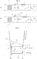
- the two portions a) and b) of Figure 1 are exemplary of the possibility of replacing one or more rectification diodes (for instance two rectification diodes D1, D2) with respective corresponding FETs (MOSFET transistors, for instance) F1 and F2 within the framework of a rectifier circuit.
- one or more rectification diodes for instance two rectification diodes D1, D2
- FETs MOSFET transistors, for instance
- This may occur, for instance, at the secondary side of a transformer T, with the MOSFET transistors F1 and F2 alternatively turned on (that is, made conductive) and off (that is, made non-conductive) under the control of a control unit CU so that a (rectified) current may flow in channels of the MOSFET transistors F1 and F2.
- the rectifier circuit architecture in Figure 1 includes two diodes D1, D2 (portion a) or two MOSFET transistors F1, F2 (portion b) coupled to the secondary winding of a transformer T and having cascaded thereto a LC lowpass filter suited to provide a (rectified) voltage signal V out to a load LD.
- One or more embodiments may comprise (digital) controller circuits suited to be coupled to field effect transistors (for instance, F1 and F2 in Figure 2 ) .
- a conventional field effect transistor such as, for instance, a MOSFET comprises a channel between source and drain terminals as well as a body diode and a gate terminal configured to control electrical current flow in the field effect transistor channel.
- SR synchronous rectification
- MOSFETs FETs
- a control logic should desirably be able to reduce progressively the conduction times of the MOSFET body diode, for instance via adaptive SR driving.
- V DS of a SR MOSFET can be sensed to detect body diode conduction by using additional hardware (i.e. comparators, etc.) to measure the conduction time. Based on this measure, the duration of the PWM "on" time can be adjusted to avoid a fast turn-off mechanism if the diode conduction time changes abruptly.
- additional hardware i.e. comparators, etc.
- Such an implementation can be resorted to, for instance, in those topologies (e.g. LLC converters) where the turn-on time may be already known to the digital controller.
- One or more embodiments may rely on a MOSFET turn-on and turn-off mechanism where (only) internal resources of a digital controller may be used to detect the start and the end of conduction of the body diode of a FET such as a MOSFET and drive the FET consequently. This may facilitate performing an adaptive SR algorithm which increases teh efficiency of the converter in a simple and reliable way.
- the drain-source voltage V DS voltage (possibly conditioned - e.g. converted to digital - as desired, in manner known per se) can be sensed and sent to an comparator (e.g. internal to the controller CD) and compared to a threshold V TH_ON_OFF , set by the controller.
- an comparator e.g. internal to the controller CD
- a digital controller CD is shown coupled to a power converter CP comprising a rectifier arrangement of one or more SR FETs such as MOSFET transistors.
- one or more embodiments may be applied to a wide variety of rectifier circuits adopting synchronous rectification.
- Figure 3 refers for simplicity to a converter circuit block CP, which may include one or more rectification FETs whose V DS voltage can be sensed with current conduction in the FET channel controlled via a PWM signal applied to the FET gate.
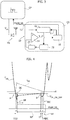
- Figure 3 refers to a single FET whose V DS voltage can be sensed via a conventional voltage sensor VS at a sensing node 10 of the digital controller CD and where current conduction in the FET channel can be controlled via a PWM signal applied to the FET gate via a drive node 12 of the digital controller CD.
- Reference 14 in Figure 3 indicates a (digital) comparator in the controller CD where, as discussed in the following, the drain-source voltage V DS sensed at 10 is compared with a reference value (e.g., V TH_ON_OFF ), with the result of comparison at 14 used to drive a PWM generator block 16 having an output coupled to the drive node 12 which controls (rectified) current flow (I SR ) in the FET channel.
- V TH_ON_OFF a reference value
- rising and falling edges of V DS at the comparator 14 can be used to trigger the PWM generator block 16 to generate at node 12 the PWM signal for driving a FET in the converter CP.
- the PWM generation block 16 (which may comprise a timer) is triggered to generate a PWM signal, designated PWM_SR (e.g., "high"), after a programmed delay (turn-on delay TOD).
- PWM_SR e.g., "high”
- the signal PWM SR is kept high for a minimum on-time (blanking window of the comparator BT) to avoid false triggers.
- the comparator output triggers via the block 16 the shutdown of PWM signal PWM_SR (see Figure 2 , left hand side), at a comparator trigger time CT earlier with respect to a normal pulse duration NP of the PWM signal.
- a single comparator with a single threshold can be used with the comparator configured to trigger alternatively, PWM signal turn-on and turn-off.
- Hysteresis possibly programmable may be present and kept at a low level in order to facilitate switching at a desired threshold. Avoiding undesired abrupt switching may be facilitated by the Blanking window feature BT discussed previously.
- two comparators with a single threshold may be used, so that a same threshold can be used for turn-on (triggered by a first comparator) and turn-off (triggered by a second comparator), so that no reconfiguration is required.
- two comparators with two (different) thresholds may be used, so that a first threshold can be used for turn-on and a second (variable) threshold can be used for turn-off.
- a single (adaptive) threshold V TH_ON_OFF will be considered in order to make the presentation simpler and facilitate understanding of the embodiments.
- Figure 4 where entities like entities already discussed in connection with Figure 2 are indicated with like references (a related description will not be repeated here for brevity) - shows that if the PWM signal PWM SR is turned-off too early, a (still) positive current I SR through the FET will causes a non-negligible body diode conduction (DC, right hand side of Figure 4 ). This implies a low converter efficiency, so that the benefits of SR are at least partially lost.
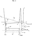
- Figure 5 where entities like entities already discussed in connection with Figures 2 and 4 are again indicated with like references (a related description will not be repeated here for brevity) - shows that if, conversely, the PWM signal PWM SR is turned-off too late, the FET will be forced to conduct even with the diode reverse-biased (DC, right hand side of Figure 5 ) and an ensuing negative current I SR can damage the MOSFET and cause its failure.
- V DS may force the body diode to conduct again, thus producing an undesired turn on: see UTO in Figure 5 ).
- the comparator 14 may be triggered again to generate an undesired PWM signal PWM_SR ( Figure 5 , bottom right) losing efficiency and keeping the FET on for a minimum "on" time.
- One or more embodiments may thus adopt an adaptive SR control logic which facilitates reducing body diode conduction time by making the comparator threshold VTH_ON_OFF adaptive.
- One or more embodiments may thus check if the threshold (V TH_ON_OFF ) of the comparator 14 is well tuned. This may occur by sampling the voltage V DS with a programmable sampling delay SD from PWM turn-off using the previous threshold value, and comparing it with a fixed value.
- An analog-to-digital converter (ADC) channel can be used to sample the drain-to-source voltage Vds (for instance at times T-ADC in Figures 4 and 5 ) of the (MOS)FET after PWM turn-off (time indicated CT in Figures 4 and 5 ) and the synchronous rectification SR control logic can change the threshold(s) in the comparator 14 by using, for instance, an digital-to-analog converter or DAC channel.
- ADC analog-to-digital converter
- the programmed delay facilitates achieving a condition where the (MOS)FET is completely turned-off because it can consider both turn-off delay and propagation delay introduced by gate drivers (both delays can be known and do not vary over time).
- the value thus obtained being found to be below the preset threshold means that the MOSFET body diode is still conducting and the PWM is turned-off too early because the voltage drop on the MOSFET is equal to the forward voltage of body diode.
- the threshold of the comparator 14 can be increased to achieve a later (delayed) MOSFET turn-off.
- the acquired value being above the preset threshold suggests that MOSFET may have been "forced” to conduct even with a reverse current and the PWM is turned-off too late. This may be related to the fact that a small safe interval, in which the diode conducts (little notch in the V DS waveform), is not present and V DS rises (too) quickly. In this case the threshold of the comparator can be decreased to turn-off the MOSFET earlier.
- the sampling delay from PWM turn-off gives also the time duration of this safe body diode conduction interval.
- reference 18 denotes a circuit block which is triggered (via a line T) by a signal provided by the PWM generator 16 to provide a delayed acquisition of the signal V DS at the input 10.
- Reference 20 denotes an adaptive SR logic acting in cooperation with the delayed acquisition block 18 and with a circuit block 22 which controls (adaptively) the threshold(s) of the comparator 14.
- the threshold of the comparator 14 can be increased and decreased within an expected range [ COMP THMIN ; COMP THMAX ] that depends on the characteristics of the sensing circuit and can be acquired with some measurements.
- a small capacitor can be added in the sensing circuit VS to reduce the slope of V DS in sensing the associated waveform and obtain a better threshold regulation.
- the flowchart of Figure 6 is exemplary of an adaptive synchronous rectification (SR) procedure which can be performed at each MOSFET turn-off or at a lower frequency (in this latter case, the comparator threshold(s) is/are kept constant over more PWM cycles).
- SR adaptive synchronous rectification
- the block 100 in the flow-chart of Figure 6 is representative of MOSFET turn-off, triggered as a result of comparing, e.g. in the comparator 14, the (conditioned) sensed value for V DS with a "previous" threshold.
- the block 102 is exemplary of V DS being sampled after a fixed delay (e.g. T-ADC) added to the FET turnoff time CT taken as starting time.
- T-ADC a fixed delay
- This operation can occur in an automatic manner in a digital controller (for instance, a STM32 microcontroller as available with companies of the ST group) even without resorting to software instructions.
- the timer may be the same as used for generating the PWM signal (PWM generator block 16) in advanced microcontrollers (a so-called “autodelayed mode” in e.g. STM32F334).
- a further timer which starts counting at a trigger event (e.g. the falling edge of the PWM signal.
- microcontroller does not include internal trigger connections one may use a further pin of the microcontroller coupled with the PWM signal and start the further timer at a falling edge (see, for instance the line T in Figure 3 ).
- the comparator trigger can be stored in a register in a timer (for instance, in the memory of the microcontroller).
- a check can be as to whether V DS as sampled is higher than a preset desired value, e.g. Vds_TH.
- a decreased value for the threshold (e.g., V TH_ON_OFF )in the comparator 14 is calculated at 106 and a check is performed at 108 as to whether the value thus calculated (not yet set) is lower than a minimum respective value, e.g. COMP THMIN .
- the check at 108 yields a positive outcome (Y) the minimum value is selected for the comparator threshold(s) .
- an increased value for the threshold (e.g., V TH_ON_OFF ) in the comparator 14 is calculated at 112 and a check is performed at 114 as to whether the value thus calculated (not yet set) is higher than a maximum respective value, e.g. COMP THMAX .
- a circuit may comprise:
- the PWM signal generator may be configured to turn the field effect transistor on with a certain delay (e.g., TOD) to the respective crossings of said at least one reference threshold by said drain-to-source voltage.
- a certain delay e.g., TOD
- the PWM signal generator may be configured to keep the field effect transistor turned on for on-time intervals in excess of a lower on-time threshold (e.g., BT).
- a lower on-time threshold e.g., BT
- One or more embodiments may comprise the adaptive network configured to compare (e.g., 104 in Figure 6 ) the drain-to-source voltage (V DS ) of the field effect transistor sensed with a certain delay (T-ADC) at said acquisition circuit block with an acquisition threshold value (for instance, V DS_TH ) and cause said field effect transistor turn off times to occur later resp. earlier (e.g. due to a change in the threshold in the comparator 14) as a result of the drain-to-source voltage of the field effect transistor sensed with a certain delay at said acquisition circuit block being below resp. above said acquisition threshold value.
- V DS drain-to-source voltage
- T-ADC certain delay
- the adaptive network may be arranged intermediate the acquisition circuit block and the comparator, the adaptive network configured to vary (see, e.g. 100 to 118 in Figure 6 ) said at least one reference threshold as a function of the drain-to-source voltage of the field effect transistor sensed with a certain delay at said acquisition circuit block.
- the controller may comprise a digital controller.
- a device such as, for instance, a converter for use in battery chargers for electronic devices, USB power delivery (USB-PD) arrangements, adapters and so on, may comprise:
- a method of driving a field effect transistor having a field effect transistor channel between source and drain terminals as well as a body diode and a gate terminal configured to control electrical current flow in the field effect transistor channel may comprise:
Landscapes
- Engineering & Computer Science (AREA)
- Power Engineering (AREA)
- Dc-Dc Converters (AREA)
- Rectifiers (AREA)
- Control Of Eletrric Generators (AREA)
- Electrophonic Musical Instruments (AREA)
- Control Of Charge By Means Of Generators (AREA)
Abstract
Description
- The description relates to synchronous rectification.
- One or more embodiments can be applied, for instance, to a variety of AC/DC and DC/DC converters.
- Converters for use in battery chargers for electronic devices, USB power delivery (USB-PD) arrangements, adapters are non-limiting examples of such applications.
- In various power conversion systems, such as AC/DC and DC/DC converters, field effect transistors or FETs (MOSFET transistors, for instance) driven by control logic can replace rectifier diodes.
- This technique, oftentimes referred to as synchronous rectification (SR), is found to improve converter efficiency. Resorting to SR facilitates reducing conduction losses insofar as the (rectified) output current flows through the MOSFET channel instead of the rectification diode, with power losses correspondingly reduced.
- Such a power converter continues to operate also if a synchronous rectification FET is not driven. This is because rectification is still provided by an internal body diode (essentially body-to-drain, with body-to-source being irrelevant insofar as this is shorted out by an internal body-to-source connection).
- The body diode (which is intrinsic to most FET types) may however exhibit poor performance: properly driving a (MOS)FET, when the body diode is forward biased, may increase system efficiency by about 3% - 4%.
- Despite the intensive activity in that area, further improved solutions are desirable.
- An object of one or more embodiments is to contribute in providing such improved solutions.
- According to one or more embodiments, that object can be achieved by means of a circuit having the features set forth in the claims that follow.
- One or more embodiments may relate to a corresponding device, e.g. a MOSFET-based synchronous rectifier in a battery charger for electronic devices, a USB power delivery (USB-PD) arrangements an adapter and so on.
- One or more embodiments may relate to a corresponding method.
- The claims are an integral part of the technical description of exemplary embodiments as provided herein.
- One or more embodiments may be based on the recognition that, while suited to be implemented with analog components (for instance dedicated ICs), synchronous rectification implemented in digital form facilitates reducing the number of components, achieving improved flexibility in devising control procedures and a higher tolerance to noise.
- One or more embodiments may provide adaptive synchronous (SR) implementation.
- One or more embodiments may be implemented with a microcontroller (such as, for instance, an STM32 microcontroller as available with companies of the ST group) by using only the internal peripherals therein.
- In one or more embodiments, an (internal) comparator may trigger a timer which in turn generates a pulse-width modulation (PWM) signal. The comparator can be reconfigured on-the-fly by a direct memory access (DMA) channel to trigger PWM shut-down (otherwise a second internal comparator can be used). An analog-to-digital converter (ADC) channel can be used to sample the drain-to-source voltage Vds of the (MOS)FET after PWM turn-off, then the synchronous rectification (SR) control logic can change the comparator threshold by using, for instance, an digital-to-analog converter or DAC channel.
- One or more embodiments will now be described, by way of example only, with reference to the annexed figures, wherein:
-
Figure 1 comprises two portions, indicated a) and b), and is representative of the possible replacement of diode rectification with synchronous rectification by means of field effect transistors (FETs) such a MOSFETs, -
Figure 2 is a time diagram exemplary of certain signals possibly involved in synchronous rectification with FETs, -
Figure 3 is a block diagram exemplary of a possible context of use of embodiments, -
Figures 4 and5 are further time diagrams exemplary of certain signals possibly involved in synchronous rectification with FETs, and -
Figure 6 is a flow chart exemplary of possible operation of embodiments. - In the ensuing description, one or more specific details are illustrated, aimed at providing an in-depth understanding of examples of embodiments of this description. The embodiments may be obtained without one or more of the specific details, or with other methods, components, materials, etc. In other cases, known structures, materials, or operations are not illustrated or described in detail so that certain aspects of embodiments will not be obscured.
- Reference to "an embodiment" or "one embodiment" in the framework of the present description is intended to indicate that a particular configuration, structure, or characteristic described in relation to the embodiment is comprised in at least one embodiment. Hence, phrases such as "in an embodiment" or "in one embodiment" that may be present in one or more points of the present description do not necessarily refer to one and the same embodiment. Moreover, particular conformations, structures, or characteristics may be combined in any adequate way in one or more embodiments.
- The references used herein are provided merely for convenience and hence do not define the extent of protection or the scope of the embodiments.
- As noted, in various power conversion systems, such as AC/DC and DC/DC converters, field effect transistors, namely FETs (MOSFET transistors, for instance) driven by control logic can replace rectifier diodes. This technique, oftentimes referred to as synchronous rectification (SR) is found to improve converter efficiency.
- The two portions a) and b) of
Figure 1 are exemplary of the possibility of replacing one or more rectification diodes (for instance two rectification diodes D1, D2) with respective corresponding FETs (MOSFET transistors, for instance) F1 and F2 within the framework of a rectifier circuit. - This may occur, for instance, at the secondary side of a transformer T, with the MOSFET transistors F1 and F2 alternatively turned on (that is, made conductive) and off (that is, made non-conductive) under the control of a control unit CU so that a (rectified) current may flow in channels of the MOSFET transistors F1 and F2.
- The rectifier circuit architecture in
Figure 1 includes two diodes D1, D2 (portion a) or two MOSFET transistors F1, F2 (portion b) coupled to the secondary winding of a transformer T and having cascaded thereto a LC lowpass filter suited to provide a (rectified) voltage signal Vout to a load LD. - It will be appreciated that the rectifier circuit architecture in
Figure 1 is just exemplary of a wide variety of rectifier circuits to which SR can be applied: therefore the circuit architecture ofFigure 1 is not to be construed, even indirectly, as confining the scope of the embodiments. - One or more embodiments may comprise (digital) controller circuits suited to be coupled to field effect transistors (for instance, F1 and F2 in
Figure 2 ) . - A conventional field effect transistor (FET) such as, for instance, a MOSFET comprises a channel between source and drain terminals as well as a body diode and a gate terminal configured to control electrical current flow in the field effect transistor channel.
- As noted, by resorting to SR, conduction losses can be reduced thanks to the output current Iout flowing through a (MOS)FET channel instead of a rectification diode, so that the power loss is decreased from P loss_diode = Vd · Iout (where Vd is the voltage drop across the diode) to P loss_MOSFET = R ds_on · Iout 2 (where R ds_on is the drain-source resistance in the "on" or conductive state) which may be (very) low for SR MOSFETs.
- As similarly noted, such a power converter continues to operate also if a synchronous rectification FET is not driven. This is because rectification is still provided by an internal body diode, which, however, may exhibit poor performance: properly driving such a MOSFET when the body diode is forward biased may increase system efficiency by about 3% - 4%.
- A problem underlying synchronous rectification (SR) using FETs (MOSFETs will be primarily referred to in the following for simplicity) is detecting the MOSFET body diode conduction in order to be able to turn-off the MOSFET channel in a fast and reliable way, thus avoiding current inversion, which may cause MOSFET failure.
- This may apply, for instance, to those systems where a digital controller has no prior information about diode conduction (e.g. because the power converter is driven by another IC). To increase the efficiency of the system, a control logic should desirably be able to reduce progressively the conduction times of the MOSFET body diode, for instance via adaptive SR driving.
- It is observed that digital solutions can be conceived where the drain-source voltage VDS of a SR MOSFET can be sensed to detect body diode conduction by using additional hardware (i.e. comparators, etc.) to measure the conduction time. Based on this measure, the duration of the PWM "on" time can be adjusted to avoid a fast turn-off mechanism if the diode conduction time changes abruptly. Such an implementation can be resorted to, for instance, in those topologies (e.g. LLC converters) where the turn-on time may be already known to the digital controller.
- One or more embodiments may rely on a MOSFET turn-on and turn-off mechanism where (only) internal resources of a digital controller may be used to detect the start and the end of conduction of the body diode of a FET such as a MOSFET and drive the FET consequently. This may facilitate performing an adaptive SR algorithm which increases teh efficiency of the converter in a simple and reliable way.
- As exemplified in the diagram of
Figure 2 , the drain-source voltage VDS voltage (possibly conditioned - e.g. converted to digital - as desired, in manner known per se) can be sensed and sent to an comparator (e.g. internal to the controller CD) and compared to a threshold VTH_ON_OFF, set by the controller. - This may occur within the framework of a circuit as exemplified in
Figure 3 . - There a digital controller CD is shown coupled to a power converter CP comprising a rectifier arrangement of one or more SR FETs such as MOSFET transistors.
- As noted, one or more embodiments may be applied to a wide variety of rectifier circuits adopting synchronous rectification.
- For that reason,
Figure 3 refers for simplicity to a converter circuit block CP, which may include one or more rectification FETs whose VDS voltage can be sensed with current conduction in the FET channel controlled via a PWM signal applied to the FET gate. - For the sake of simplicity,
Figure 3 refers to a single FET whose VDS voltage can be sensed via a conventional voltage sensor VS at asensing node 10 of the digital controller CD and where current conduction in the FET channel can be controlled via a PWM signal applied to the FET gate via adrive node 12 of the digital controller CD. - For the sake of explanation it will be assumed that a "high" state of the PWM signal is intended to cause the FET to be conductive (turned on) and that a "low" state of the PWM signal is intended to cause the FET to be non-conductive (turned off). Of course, adopting such an option is not mandatory.
-
Reference 14 inFigure 3 indicates a (digital) comparator in the controller CD where, as discussed in the following, the drain-source voltage VDS sensed at 10 is compared with a reference value (e.g., VTH_ON_OFF), with the result of comparison at 14 used to drive aPWM generator block 16 having an output coupled to thedrive node 12 which controls (rectified) current flow (ISR) in the FET channel. - In one or more embodiments, rising and falling edges of VDS at the comparator 14 (that is crossings of the threshold (s) of the
comparator 14 by VDS) can be used to trigger thePWM generator block 16 to generate atnode 12 the PWM signal for driving a FET in the converter CP. - For instance, as exemplified in
Figure 2 , when the voltage VDS decreases below the threshold of the comparator 14 (falling edge at the comparator output - see point A inFigure 2 - which is indicative of the body diode conducting), the PWM generation block 16 (which may comprise a timer) is triggered to generate a PWM signal, designated PWM_SR (e.g., "high"), after a programmed delay (turn-on delay TOD). - The signal PWM SR is kept high for a minimum on-time (blanking window of the comparator BT) to avoid false triggers.
- A result of VDS rising again above the threshold (rising edge at the comparator output - see point B in
Figure 2 - which means that the body diode is going to be reverse biased), the comparator output triggers via theblock 16 the shutdown of PWM signal PWM_SR (seeFigure 2 , left hand side), at a comparator trigger time CT earlier with respect to a normal pulse duration NP of the PWM signal. - Intervals of body diode conduction at points A and B are indicated as DC (body diode conduction).
- It will be appreciated that, in one or more embodiments, various options may be resorted to in order to facilitate this kind of operation.
- For instance, a single comparator with a single threshold can be used with the comparator configured to trigger alternatively, PWM signal turn-on and turn-off. Hysteresis (possibly programmable) may be present and kept at a low level in order to facilitate switching at a desired threshold. Avoiding undesired abrupt switching may be facilitated by the Blanking window feature BT discussed previously.
- In one or more embodiments, two comparators with a single threshold may be used, so that a same threshold can be used for turn-on (triggered by a first comparator) and turn-off (triggered by a second comparator), so that no reconfiguration is required.
- In one or more embodiments, two comparators with two (different) thresholds may be used, so that a first threshold can be used for turn-on and a second (variable) threshold can be used for turn-off.
- In this description of exemplary embodiments, a single (adaptive) threshold VTH_ON_OFF will be considered in order to make the presentation simpler and facilitate understanding of the embodiments.
-
Figure 4 - where entities like entities already discussed in connection withFigure 2 are indicated with like references (a related description will not be repeated here for brevity) - shows that if the PWM signal PWM SR is turned-off too early, a (still) positive current ISR through the FET will causes a non-negligible body diode conduction (DC, right hand side ofFigure 4 ). This implies a low converter efficiency, so that the benefits of SR are at least partially lost. -
Figure 5 - where entities like entities already discussed in connection withFigures 2 and4 are again indicated with like references (a related description will not be repeated here for brevity) - shows that if, conversely, the PWM signal PWM SR is turned-off too late, the FET will be forced to conduct even with the diode reverse-biased (DC, right hand side ofFigure 5 ) and an ensuing negative current ISR can damage the MOSFET and cause its failure. - Moreover, after FET turn-off, a voltage ringing of VDS may force the body diode to conduct again, thus producing an undesired turn on: see UTO in
Figure 5 ). Thecomparator 14 may be triggered again to generate an undesired PWM signal PWM_SR (Figure 5 , bottom right) losing efficiency and keeping the FET on for a minimum "on" time. - One or more embodiments may thus adopt an adaptive SR control logic which facilitates reducing body diode conduction time by making the comparator threshold VTH_ON_OFF adaptive.
- One or more embodiments may thus check if the threshold (VTH_ON_OFF) of the
comparator 14 is well tuned. This may occur by sampling the voltage VDS with a programmable sampling delay SD from PWM turn-off using the previous threshold value, and comparing it with a fixed value. - An analog-to-digital converter (ADC) channel can be used to sample the drain-to-source voltage Vds (for instance at times T-ADC in
Figures 4 and5 ) of the (MOS)FET after PWM turn-off (time indicated CT inFigures 4 and5 ) and the synchronous rectification SR control logic can change the threshold(s) in thecomparator 14 by using, for instance, an digital-to-analog converter or DAC channel. - The programmed delay facilitates achieving a condition where the (MOS)FET is completely turned-off because it can consider both turn-off delay and propagation delay introduced by gate drivers (both delays can be known and do not vary over time).
- The value thus obtained being found to be below the preset threshold (see right hand side of
Figure 4 ) means that the MOSFET body diode is still conducting and the PWM is turned-off too early because the voltage drop on the MOSFET is equal to the forward voltage of body diode. In this case the threshold of thecomparator 14 can be increased to achieve a later (delayed) MOSFET turn-off. - Otherwise, the acquired value being above the preset threshold (see right hand side of
Figure 5 ) suggests that MOSFET may have been "forced" to conduct even with a reverse current and the PWM is turned-off too late. This may be related to the fact that a small safe interval, in which the diode conducts (little notch in the VDS waveform), is not present and VDS rises (too) quickly. In this case the threshold of the comparator can be decreased to turn-off the MOSFET earlier. - The sampling delay from PWM turn-off (times CT in
Figures 2 ,4 and5 ) gives also the time duration of this safe body diode conduction interval. - In the block diagram of
Figure 3 ,reference 18 denotes a circuit block which is triggered (via a line T) by a signal provided by thePWM generator 16 to provide a delayed acquisition of the signal VDS at theinput 10. -
Reference 20 denotes an adaptive SR logic acting in cooperation with the delayedacquisition block 18 and with acircuit block 22 which controls (adaptively) the threshold(s) of thecomparator 14. - In one or more embodiments, the threshold of the
comparator 14 can be increased and decreased within an expected range [COMPTHMIN ; COMPTHMAX ] that depends on the characteristics of the sensing circuit and can be acquired with some measurements. - A small capacitor can be added in the sensing circuit VS to reduce the slope of VDS in sensing the associated waveform and obtain a better threshold regulation.
- The flowchart of
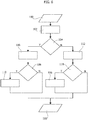
Figure 6 is exemplary of an adaptive synchronous rectification (SR) procedure which can be performed at each MOSFET turn-off or at a lower frequency (in this latter case, the comparator threshold(s) is/are kept constant over more PWM cycles). - The
block 100 in the flow-chart ofFigure 6 is representative of MOSFET turn-off, triggered as a result of comparing, e.g. in thecomparator 14, the (conditioned) sensed value for VDS with a "previous" threshold. - The
block 102 is exemplary of VDS being sampled after a fixed delay (e.g. T-ADC) added to the FET turnoff time CT taken as starting time. This operation can occur in an automatic manner in a digital controller (for instance, a STM32 microcontroller as available with companies of the ST group) even without resorting to software instructions. - For instance (as a function of the type of controller) the possibility exists of adding a certain (predetermined) delay starting from an (external) event such as the comparator trigger to an internal timer of the controller.
- The timer may be the same as used for generating the PWM signal (PWM generator block 16) in advanced microcontrollers (a so-called "autodelayed mode" in e.g. STM32F334).
- Alternatively, one may use a further timer which starts counting at a trigger event (e.g. the falling edge of the PWM signal.
- If the microcontroller does not include internal trigger connections one may use a further pin of the microcontroller coupled with the PWM signal and start the further timer at a falling edge (see, for instance the line T in
Figure 3 ). - As a result of the timer reaching a certain count value (that is, after T-ADC has lapsed), a (sampling) ADC is triggered.
- In one or more embodiments the comparator trigger can be stored in a register in a timer (for instance, in the memory of the microcontroller).
- With the measurement result received from the ADC triggered at a desired time, in a block 104 a check can be as to whether VDS as sampled is higher than a preset desired value, e.g. Vds_TH.
- If the check at 104 yields a positive outcome (Y), a decreased value for the threshold (e.g., VTH_ON_OFF)in the
comparator 14 is calculated at 106 and a check is performed at 108 as to whether the value thus calculated (not yet set) is lower than a minimum respective value, e.g. COMPTHMIN . - If the check at 108 yields a positive outcome (Y) the minimum value is selected for the comparator threshold(s) .
- If the check at 104 yields a negative outcome (N), an increased value for the threshold (e.g., VTH_ON_OFF) in the
comparator 14 is calculated at 112 and a check is performed at 114 as to whether the value thus calculated (not yet set) is higher than a maximum respective value, e.g. COMPTHMAX. - If the check at 114 yields a positive outcome (Y) the maximum value is selected for the comparator threshold(s) .
- Starting from any of:
- the
block 110; - a negative outcome (N) of the check at 108;
- the
block 116; - a negative outcome (N) of the check at 114,
- In one or more embodiments, a circuit may comprise:
- a controller (e.g., CD) configured for coupling to a field effect transistor (e.g., as included in CP in
Figure 3 ) having a field effect transistor channel between source and drain terminals as well as a body diode and a gate terminal configured to control electrical current flow in the field effect transistor channel, wherein the controller may comprise: - a sensing port (e.g., 10) configured to sense (e.g.,VS) the drain-to-source voltage (e.g., VDS) of said field effect transistor as well as a drive port (e.g., 12) configured to drive the gate terminal of the field effect transistor to alternatively turn the field effect transistor on and off to provide a rectified current flow in the field effect transistor channel,
- a comparator (e.g., 14) coupled to the sensing port, the comparator configured to perform a comparison of the drain-to-source voltage of the field effect transistor with at least one reference threshold (e.g., VTH_ON_OFF: as noted, a single threshold is discussed for simplicity) and detect alternate downward (e.g., A) and upward (e.g., B) crossings of said at least one reference threshold by said drain-to-source voltage,
- a PWM signal generator (e.g., 16) coupled to the comparator circuit and the drive port, the PWM signal generator configured to drive (e.g., PWM SR) the gate terminal of the field effect transistor to turn the field effect transistor on and off as a result of said alternate downward and upward crossings of said at least one reference threshold by said drain-to-source voltage.
- In one or more embodiments, the PWM signal generator may be configured to turn the field effect transistor on with a certain delay (e.g., TOD) to the respective crossings of said at least one reference threshold by said drain-to-source voltage.
- In one or more embodiments, the PWM signal generator may be configured to keep the field effect transistor turned on for on-time intervals in excess of a lower on-time threshold (e.g., BT).
- One or more embodiments may comprise:
- an acquisition circuit block (e.g., 18) coupled (e.g., at T) to the PWM signal generator in the controller wherein the acquisition circuit block is sensitive to field effect transistor turn off times (e.g., CT), the acquisition circuit block coupled to the sensing port and configured to sense the drain-to-source voltage of the field effect transistor with a certain delay (e.g., T-ADC) to field effect transistor turn off times,
- an adaptive network (e.g., 20, 22) coupled to the acquisition circuit block in the controller, the adaptive network configured to control said field effect transistor turn off times as a function of the drain-to-source voltage of the field effect transistor sensed with a certain delay at said acquisition circuit block.
- One or more embodiments may comprise the adaptive network configured to compare (e.g., 104 in
Figure 6 ) the drain-to-source voltage (VDS) of the field effect transistor sensed with a certain delay (T-ADC) at said acquisition circuit block with an acquisition threshold value (for instance, VDS_TH) and cause said field effect transistor turn off times to occur later resp. earlier (e.g. due to a change in the threshold in the comparator 14) as a result of the drain-to-source voltage of the field effect transistor sensed with a certain delay at said acquisition circuit block being below resp. above said acquisition threshold value. - In one or more embodiments the adaptive network may be arranged intermediate the acquisition circuit block and the comparator, the adaptive network configured to vary (see, e.g. 100 to 118 in
Figure 6 ) said at least one reference threshold as a function of the drain-to-source voltage of the field effect transistor sensed with a certain delay at said acquisition circuit block. - In one or more embodiments, the controller may comprise a digital controller.
- In one or more embodiments, a device such as, for instance, a converter for use in battery chargers for electronic devices, USB power delivery (USB-PD) arrangements, adapters and so on, may comprise:
- a rectification network (e.g., T, L, C, F1, F2 in
Figure 1 ) comprising at least one field effect transistor having a field effect transistor channel between source and drain terminals as well as a body diode and a gate terminal configured to control electrical current flow in the field effect transistor channel, - a circuit according to one or more embodiments, having the sensing port coupled to the at least one field effect transistor and configured (e.g. VS) to sense the drain-to-source voltage of said at least one field effect transistor and the drive port coupled to the gate terminal of said at least one field effect transistor to alternatively turn said at least one field effect transistor on and off to provide a rectified current flow in the channel thereof.
- In one or more embodiments, a method of driving a field effect transistor having a field effect transistor channel between source and drain terminals as well as a body diode and a gate terminal configured to control electrical current flow in the field effect transistor channel, may comprise:
- sensing the drain-to-source voltage of the field effect transistor and driving the gate terminal of the field effect transistor to alternatively turn the field effect transistor on and off to provide a rectified current flow in the field effect transistor channel,
- performing a comparison of the drain-to-source voltage of the field effect transistor with at least one reference threshold and detecting alternate downward and upward crossings of said at least one reference threshold by said drain-to-source voltage,
- driving the gate terminal of the field effect transistor by turning the field effect transistor on and off as a result of said alternate downward and upward crossings of said at least one reference threshold by said drain-to-source voltage.
- Without prejudice to the underlying principles, the details and embodiments may vary, even significantly, with respect to what has been described by way of example only, without departing from the extent of protection.
- The extent of protection is determined by the annexed claims.
Claims (9)
- A circuit, comprising:- a controller (CD) configured for coupling to a field effect transistor (CP) having a field effect transistor channel between source and drain terminals as well as a body diode and a gate terminal configured to control electrical current flow in the field effect transistor channel, wherein the controller (CD) comprises:- a sensing port (10) configured to sense (VS) the drain-to-source voltage (VDS) of said field effect transistor as well as a drive port (12) configured to drive the gate terminal of the field effect transistor to alternatively turn the field effect transistor on and off to provide a rectified current flow in the field effect transistor channel,- a comparator (14) coupled to the sensing port (10), the comparator configured to perform a comparison of the drain-to-source voltage (VDS) of the field effect transistor with at least one reference threshold (VTH_ON_OFF) and detect alternate downward (A) and upward (B) crossings of said at least one reference threshold by said drain-to-source voltage (VDS),- a PWM signal generator (16) coupled to the comparator circuit (14) and the drive port (12), the PWM signal generator (16) configured to drive (PWM_SR) the gate terminal of the field effect transistor to turn the field effect transistor on and off as a result of said alternate downward (A) and upward (B) crossings of said at least one reference threshold by said drain-to-source voltage (VDS).
- The circuit of claim 1, wherein the PWM signal generator (16) is configured to turn the field effect transistor on with a certain delay (TOD) to the respective crossings (A) of said at least one reference threshold by said drain-to-source voltage (VDS).
- The circuit of claim 1 or claim 2, wherein the PWM signal generator (16) is configured to keep the field effect transistor turned on for on-time intervals in excess of a lower on-time threshold (BT).
- The circuit of any of the previous claims, comprising:- an acquisition circuit block (18) coupled (T) to the PWM signal generator (16) in the controller (CD) wherein the acquisition circuit block (18) is sensitive to field effect transistor turn off times (CT), the acquisition circuit block (18) coupled to the sensing port (10) and configured to sense the drain-to-source voltage (VDS) of the field effect transistor with a certain delay (T-ADC) to field effect transistor turn off times (CT),- an adaptive network (20, 22) coupled to the acquisition circuit block (18) in the controller (CD), the adaptive network (20, 22) configured to control (22) said field effect transistor turn off times (CT) as a function of the drain-to-source voltage (VDS) of the field effect transistor sensed with a certain delay (T-ADC) at said acquisition circuit block (18).
- The circuit of claim 4, comprising the adaptive network (20, 22) configured to compare (104) the drain-to-source voltage (VDS) of the field effect transistor sensed with a certain delay (T-ADC) at said acquisition circuit block (18) with an acquisition threshold value to cause said field effect transistor turn off times (CT) to occur later resp. earlier as a result of the drain-to-source voltage (VDS) of the field effect transistor sensed with a certain delay (T-ADC) at said acquisition circuit block (18) being below resp. above said acquisition threshold value.
- The circuit of claim 4 or claim 5 comprising the adaptive network (20, 22) arranged intermediate the acquisition circuit block (18) and the comparator (14), the adaptive network configured to vary (100 to 118) said at least one reference threshold (VTH_ON_OFF) as a function of the drain-to-source voltage (VDS) of the field effect transistor sensed with a certain delay (T-ADC) at said acquisition circuit block (18).
- The circuit of any of the previous claims, wherein the controller (CD) comprises a digital controller.
- A device, comprising:- a rectification network (T, L, C, F1, F2) comprising at least one field effect transistor (F1, F2) having a field effect transistor channel between source and drain terminals as well as a body diode and a gate terminal configured to control electrical current flow in the field effect transistor channel,- a circuit according to any of claims 1 to 7 having the sensing port (10) coupled (VS) to the at least one field effect transistor and configured to sense the drain-to-source voltage (VDS) of said at least one field effect transistor and the drive port (12) coupled to the gate terminal of said at least one field effect transistor to alternatively turn said at least one field effect transistor on and off to provide a rectified current flow in the channel thereof.
- A method of driving a field effect transistor (CP) having a field effect transistor channel between source and drain terminals as well as a body diode and a gate terminal configured to control electrical current flow in the field effect transistor channel, the method comprising:- sensing (10) the drain-to-source voltage (VDS) of the field effect transistor and driving (12) the gate terminal of the field effect transistor to alternatively turn the field effect transistor on and off to provide a rectified current flow in the field effect transistor channel,- performing a comparison of the drain-to-source voltage (VDS) of the field effect transistor with at least one reference threshold (VTH_ON_OFF) and detecting alternate downward (A) and upward (B) crossings of said at least one reference threshold by said drain-to-source voltage (VDS),- driving (PWM_SR) the gate terminal of the field effect transistor by turning the field effect transistor on and off as a result of said alternate downward (A) and upward (B) crossings of said at least one reference threshold by said drain-to-source voltage (VDS).
Applications Claiming Priority (1)
| Application Number | Priority Date | Filing Date | Title |
|---|---|---|---|
| IT102018000004743A IT201800004743A1 (en) | 2018-04-20 | 2018-04-20 | SYNCHRONOUS RECTIFIER CIRCUIT, CORRESPONDING DEVICE AND PROCEDURE |
Publications (2)
| Publication Number | Publication Date |
|---|---|
| EP3557744A1 true EP3557744A1 (en) | 2019-10-23 |
| EP3557744B1 EP3557744B1 (en) | 2021-09-22 |
Family
ID=62751484
Family Applications (1)
| Application Number | Title | Priority Date | Filing Date |
|---|---|---|---|
| EP19164000.2A Active EP3557744B1 (en) | 2018-04-20 | 2019-03-20 | A synchronous rectification circuit, corresponding device and method |
Country Status (4)
| Country | Link |
|---|---|
| US (1) | US10658917B2 (en) |
| EP (1) | EP3557744B1 (en) |
| CN (2) | CN110391759B (en) |
| IT (1) | IT201800004743A1 (en) |
Families Citing this family (8)
| Publication number | Priority date | Publication date | Assignee | Title |
|---|---|---|---|---|
| IT201800004743A1 (en) * | 2018-04-20 | 2019-10-20 | SYNCHRONOUS RECTIFIER CIRCUIT, CORRESPONDING DEVICE AND PROCEDURE | |
| US11323017B2 (en) * | 2020-05-29 | 2022-05-03 | Dialog Semiconductor Inc. | Adaptive gate regulation for a synchronous rectifier flyback converter |
| US11621646B2 (en) * | 2020-05-29 | 2023-04-04 | Dialog Semiconductor Inc. | Adaptive gate regulation for a synchronous rectifier flyback converter |
| US11621645B2 (en) | 2020-06-04 | 2023-04-04 | Stmicroelectronics International N.V. | Methods and device to drive a transistor for synchronous rectification |
| DE102020207055A1 (en) * | 2020-06-05 | 2021-12-09 | Continental Teves Ag & Co. Ohg | Monitoring an ideal diode |
| US11817791B2 (en) * | 2020-10-06 | 2023-11-14 | Stmicroelectronics S.R.L. | Synchronous rectifier driver circuit, related integrated circuit, electronic resonant converter and method |
| CN112821768B (en) * | 2020-12-28 | 2022-07-29 | 西安电子科技大学芜湖研究院 | Flyback synchronous rectification circuit |
| CN115514234A (en) * | 2022-06-25 | 2022-12-23 | 广州金升阳科技有限公司 | A synchronous rectification circuit and its control method |
Citations (4)
| Publication number | Priority date | Publication date | Assignee | Title |
|---|---|---|---|---|
| US20100124086A1 (en) * | 2008-11-20 | 2010-05-20 | Silergy Technology | High efficiency synchronous reectifiers |
| US20110096578A1 (en) * | 2009-10-22 | 2011-04-28 | Bcd Semiconductor Manufacturing Limited | System and method for synchronous rectifier |
| US20150049521A1 (en) * | 2013-08-14 | 2015-02-19 | Dora S.P.A. | Control device for a rectifier of a switching converter |
| US20160294298A1 (en) * | 2015-04-04 | 2016-10-06 | Joulwatt Technology Inc Limited | Body diode conduction optimization in mosfet synchronous rectifier |
Family Cites Families (16)
| Publication number | Priority date | Publication date | Assignee | Title |
|---|---|---|---|---|
| US6055170A (en) * | 1997-06-02 | 2000-04-25 | Srmos, Inc. | Prediction methods and circuits for operating a transistor as a rectifier |
| US8064229B2 (en) * | 2008-11-11 | 2011-11-22 | Semiconductor Components Industries, Llc | Method of forming a series resonant switching power supply control circuit and structure therefor |
| TWI401866B (en) * | 2010-07-20 | 2013-07-11 | Niko Semiconductor Co Ltd | Predicting-type synchronous rectification controller, switching power converter with the predicting-type synchronous rectification controller and controlling method thereof |
| US9906147B2 (en) * | 2011-09-14 | 2018-02-27 | Futurewei Technologies, Inc. | Adaptive dead time control apparatus and method for switching power converters |
| JP5867141B2 (en) * | 2012-02-17 | 2016-02-24 | ミツミ電機株式会社 | Switching power supply |
| JP2014090534A (en) * | 2012-10-29 | 2014-05-15 | Sanken Electric Co Ltd | Synchronous rectification circuit |
| US9001532B2 (en) * | 2013-01-09 | 2015-04-07 | Semiconductor Components Industries, Llc | Method of forming a synchronous rectifier controller and structure therefor |
| CN103236795B (en) * | 2013-05-10 | 2015-09-16 | 矽力杰半导体技术(杭州)有限公司 | Synchronous commutating control circuit and method |
| CN103490605B (en) * | 2013-10-12 | 2015-12-23 | 成都芯源系统有限公司 | Isolated switch converter and controller and control method thereof |
| US9236809B2 (en) * | 2013-10-16 | 2016-01-12 | Texas Instruments Incorporated | Automatic timing adjustment for synchronous rectifier circuit |
| CN103997223B (en) * | 2014-05-16 | 2016-09-07 | 西安唯电电气技术有限公司 | A kind of synchronous rectification driving circuit |
| CN105529939B (en) * | 2014-09-30 | 2018-01-23 | 万国半导体股份有限公司 | Individually encapsulation synchronous rectifier |
| CN105119505B (en) * | 2015-09-14 | 2017-11-07 | 矽力杰半导体技术(杭州)有限公司 | A kind of synchronous rectification control method and circuit of synchronous rectification |
| CN106130378B (en) * | 2016-08-31 | 2019-05-21 | 广州金升阳科技有限公司 | Synchronous rectification control circuit and method |
| US10992234B2 (en) * | 2018-01-23 | 2021-04-27 | Semiconductor Components Industries, Llc | Adaptive control of synchronous rectifier switching device |
| IT201800004743A1 (en) * | 2018-04-20 | 2019-10-20 | SYNCHRONOUS RECTIFIER CIRCUIT, CORRESPONDING DEVICE AND PROCEDURE |
-
2018
- 2018-04-20 IT IT102018000004743A patent/IT201800004743A1/en unknown
-
2019
- 2019-03-20 EP EP19164000.2A patent/EP3557744B1/en active Active
- 2019-04-01 US US16/371,489 patent/US10658917B2/en active Active
- 2019-04-17 CN CN201910308755.0A patent/CN110391759B/en active Active
- 2019-04-17 CN CN201920521421.7U patent/CN209930162U/en active Active
Patent Citations (4)
| Publication number | Priority date | Publication date | Assignee | Title |
|---|---|---|---|---|
| US20100124086A1 (en) * | 2008-11-20 | 2010-05-20 | Silergy Technology | High efficiency synchronous reectifiers |
| US20110096578A1 (en) * | 2009-10-22 | 2011-04-28 | Bcd Semiconductor Manufacturing Limited | System and method for synchronous rectifier |
| US20150049521A1 (en) * | 2013-08-14 | 2015-02-19 | Dora S.P.A. | Control device for a rectifier of a switching converter |
| US20160294298A1 (en) * | 2015-04-04 | 2016-10-06 | Joulwatt Technology Inc Limited | Body diode conduction optimization in mosfet synchronous rectifier |
Also Published As
| Publication number | Publication date |
|---|---|
| US10658917B2 (en) | 2020-05-19 |
| CN110391759B (en) | 2021-11-12 |
| US20190326808A1 (en) | 2019-10-24 |
| CN110391759A (en) | 2019-10-29 |
| CN209930162U (en) | 2020-01-10 |
| EP3557744B1 (en) | 2021-09-22 |
| IT201800004743A1 (en) | 2019-10-20 |
Similar Documents
| Publication | Publication Date | Title |
|---|---|---|
| US10658917B2 (en) | Synchronous rectification circuit, corresponding device and method | |
| US10468975B2 (en) | Flyback converter, active clamp control circuit and active clamp control method | |
| KR102195552B1 (en) | Gate driver for switching converter having body diode power loss minimization | |
| US6958592B2 (en) | Adaptive delay control circuit for switched mode power supply | |
| US7906948B2 (en) | Threshold voltage monitoring and control in synchronous power converters | |
| US10516338B2 (en) | Voltage converter controller, voltage converter and method for operating a voltage converter | |
| US9735686B2 (en) | Device for avoiding hard switching in resonant converter and related method | |
| US11942925B2 (en) | Management of multiple switching-synchronized measurements using combined prioritized measurement and round-robin sequence measurement | |
| KR102609990B1 (en) | Adaptive Gate Drive for A Power Switch Transistor in A Switching Power Converter | |
| CN104811018B (en) | Self-timing for circuit of synchronous rectification adjusts | |
| US20130063985A1 (en) | Adaptive Dead Time Control Apparatus and Method for Switching Power Converters | |
| CN116054610B (en) | AC-DC converter, controller, driving system and driving method | |
| US10622910B2 (en) | Semiconductor device and method of operating the same | |
| CN113098286A (en) | Synchronous rectification method for LCLCLCL resonant converter | |
| US10536088B2 (en) | Switched mode power supply controller | |
| US11621645B2 (en) | Methods and device to drive a transistor for synchronous rectification | |
| US11984809B2 (en) | CCM-based fly-back switching power supply circuit and control method thereof | |
| US20260074691A1 (en) | GaN Gate Driver for EMI Optimization During Turn-on and Turn-off | |
| US7397290B2 (en) | Method and relative circuit for generating a control voltage of a synchronous rectifier | |
| US10804810B2 (en) | DC-DC converter and a method for controlling a DC-DC converter | |
| US7880329B2 (en) | Multi-channel switching regulator | |
| CN209120063U (en) | Switch circuit control circuit and switch circuit | |
| CN219535881U (en) | Dead zone control circuit and switching power supply | |
| US20260074607A1 (en) | Advanced Gate Driver for Improved EMI Performance During MOSFET Turn-on | |
| US12047001B2 (en) | Zero-crossing correction circuit and zero-crossing correction method for a switching converter |
Legal Events
| Date | Code | Title | Description |
|---|---|---|---|
| PUAI | Public reference made under article 153(3) epc to a published international application that has entered the european phase |
Free format text: ORIGINAL CODE: 0009012 |
|
| STAA | Information on the status of an ep patent application or granted ep patent |
Free format text: STATUS: THE APPLICATION HAS BEEN PUBLISHED |
|
| AK | Designated contracting states |
Kind code of ref document: A1 Designated state(s): AL AT BE BG CH CY CZ DE DK EE ES FI FR GB GR HR HU IE IS IT LI LT LU LV MC MK MT NL NO PL PT RO RS SE SI SK SM TR |
|
| AX | Request for extension of the european patent |
Extension state: BA ME |
|
| STAA | Information on the status of an ep patent application or granted ep patent |
Free format text: STATUS: REQUEST FOR EXAMINATION WAS MADE |
|
| 17P | Request for examination filed |
Effective date: 20191218 |
|
| RBV | Designated contracting states (corrected) |
Designated state(s): AL AT BE BG CH CY CZ DE DK EE ES FI FR GB GR HR HU IE IS IT LI LT LU LV MC MK MT NL NO PL PT RO RS SE SI SK SM TR |
|
| STAA | Information on the status of an ep patent application or granted ep patent |
Free format text: STATUS: EXAMINATION IS IN PROGRESS |
|
| 17Q | First examination report despatched |
Effective date: 20200415 |
|
| GRAP | Despatch of communication of intention to grant a patent |
Free format text: ORIGINAL CODE: EPIDOSNIGR1 |
|
| STAA | Information on the status of an ep patent application or granted ep patent |
Free format text: STATUS: GRANT OF PATENT IS INTENDED |
|
| RIC1 | Information provided on ipc code assigned before grant |
Ipc: H02M 1/00 20060101ALN20210326BHEP Ipc: H02M 3/335 20060101AFI20210326BHEP |
|
| INTG | Intention to grant announced |
Effective date: 20210504 |
|
| GRAS | Grant fee paid |
Free format text: ORIGINAL CODE: EPIDOSNIGR3 |
|
| GRAA | (expected) grant |
Free format text: ORIGINAL CODE: 0009210 |
|
| STAA | Information on the status of an ep patent application or granted ep patent |
Free format text: STATUS: THE PATENT HAS BEEN GRANTED |
|
| AK | Designated contracting states |
Kind code of ref document: B1 Designated state(s): AL AT BE BG CH CY CZ DE DK EE ES FI FR GB GR HR HU IE IS IT LI LT LU LV MC MK MT NL NO PL PT RO RS SE SI SK SM TR |
|
| REG | Reference to a national code |
Ref country code: GB Ref legal event code: FG4D |
|
| REG | Reference to a national code |
Ref country code: IE Ref legal event code: FG4D |
|
| REG | Reference to a national code |
Ref country code: DE Ref legal event code: R096 Ref document number: 602019007777 Country of ref document: DE |
|
| REG | Reference to a national code |
Ref country code: CH Ref legal event code: EP Ref country code: AT Ref legal event code: REF Ref document number: 1433087 Country of ref document: AT Kind code of ref document: T Effective date: 20211015 |
|
| REG | Reference to a national code |
Ref country code: LT Ref legal event code: MG9D |
|
| REG | Reference to a national code |
Ref country code: NL Ref legal event code: MP Effective date: 20210922 |
|
| PG25 | Lapsed in a contracting state [announced via postgrant information from national office to epo] |
Ref country code: FI Free format text: LAPSE BECAUSE OF FAILURE TO SUBMIT A TRANSLATION OF THE DESCRIPTION OR TO PAY THE FEE WITHIN THE PRESCRIBED TIME-LIMIT Effective date: 20210922 Ref country code: RS Free format text: LAPSE BECAUSE OF FAILURE TO SUBMIT A TRANSLATION OF THE DESCRIPTION OR TO PAY THE FEE WITHIN THE PRESCRIBED TIME-LIMIT Effective date: 20210922 Ref country code: SE Free format text: LAPSE BECAUSE OF FAILURE TO SUBMIT A TRANSLATION OF THE DESCRIPTION OR TO PAY THE FEE WITHIN THE PRESCRIBED TIME-LIMIT Effective date: 20210922 Ref country code: HR Free format text: LAPSE BECAUSE OF FAILURE TO SUBMIT A TRANSLATION OF THE DESCRIPTION OR TO PAY THE FEE WITHIN THE PRESCRIBED TIME-LIMIT Effective date: 20210922 Ref country code: NO Free format text: LAPSE BECAUSE OF FAILURE TO SUBMIT A TRANSLATION OF THE DESCRIPTION OR TO PAY THE FEE WITHIN THE PRESCRIBED TIME-LIMIT Effective date: 20211222 Ref country code: BG Free format text: LAPSE BECAUSE OF FAILURE TO SUBMIT A TRANSLATION OF THE DESCRIPTION OR TO PAY THE FEE WITHIN THE PRESCRIBED TIME-LIMIT Effective date: 20211222 Ref country code: LT Free format text: LAPSE BECAUSE OF FAILURE TO SUBMIT A TRANSLATION OF THE DESCRIPTION OR TO PAY THE FEE WITHIN THE PRESCRIBED TIME-LIMIT Effective date: 20210922 |
|
| REG | Reference to a national code |
Ref country code: AT Ref legal event code: MK05 Ref document number: 1433087 Country of ref document: AT Kind code of ref document: T Effective date: 20210922 |
|
| PG25 | Lapsed in a contracting state [announced via postgrant information from national office to epo] |
Ref country code: LV Free format text: LAPSE BECAUSE OF FAILURE TO SUBMIT A TRANSLATION OF THE DESCRIPTION OR TO PAY THE FEE WITHIN THE PRESCRIBED TIME-LIMIT Effective date: 20210922 Ref country code: GR Free format text: LAPSE BECAUSE OF FAILURE TO SUBMIT A TRANSLATION OF THE DESCRIPTION OR TO PAY THE FEE WITHIN THE PRESCRIBED TIME-LIMIT Effective date: 20211223 |
|
| PG25 | Lapsed in a contracting state [announced via postgrant information from national office to epo] |
Ref country code: AT Free format text: LAPSE BECAUSE OF FAILURE TO SUBMIT A TRANSLATION OF THE DESCRIPTION OR TO PAY THE FEE WITHIN THE PRESCRIBED TIME-LIMIT Effective date: 20210922 |
|
| PG25 | Lapsed in a contracting state [announced via postgrant information from national office to epo] |
Ref country code: IS Free format text: LAPSE BECAUSE OF FAILURE TO SUBMIT A TRANSLATION OF THE DESCRIPTION OR TO PAY THE FEE WITHIN THE PRESCRIBED TIME-LIMIT Effective date: 20220122 Ref country code: SK Free format text: LAPSE BECAUSE OF FAILURE TO SUBMIT A TRANSLATION OF THE DESCRIPTION OR TO PAY THE FEE WITHIN THE PRESCRIBED TIME-LIMIT Effective date: 20210922 Ref country code: RO Free format text: LAPSE BECAUSE OF FAILURE TO SUBMIT A TRANSLATION OF THE DESCRIPTION OR TO PAY THE FEE WITHIN THE PRESCRIBED TIME-LIMIT Effective date: 20210922 Ref country code: PT Free format text: LAPSE BECAUSE OF FAILURE TO SUBMIT A TRANSLATION OF THE DESCRIPTION OR TO PAY THE FEE WITHIN THE PRESCRIBED TIME-LIMIT Effective date: 20220124 Ref country code: PL Free format text: LAPSE BECAUSE OF FAILURE TO SUBMIT A TRANSLATION OF THE DESCRIPTION OR TO PAY THE FEE WITHIN THE PRESCRIBED TIME-LIMIT Effective date: 20210922 Ref country code: NL Free format text: LAPSE BECAUSE OF FAILURE TO SUBMIT A TRANSLATION OF THE DESCRIPTION OR TO PAY THE FEE WITHIN THE PRESCRIBED TIME-LIMIT Effective date: 20210922 Ref country code: ES Free format text: LAPSE BECAUSE OF FAILURE TO SUBMIT A TRANSLATION OF THE DESCRIPTION OR TO PAY THE FEE WITHIN THE PRESCRIBED TIME-LIMIT Effective date: 20210922 Ref country code: EE Free format text: LAPSE BECAUSE OF FAILURE TO SUBMIT A TRANSLATION OF THE DESCRIPTION OR TO PAY THE FEE WITHIN THE PRESCRIBED TIME-LIMIT Effective date: 20210922 Ref country code: CZ Free format text: LAPSE BECAUSE OF FAILURE TO SUBMIT A TRANSLATION OF THE DESCRIPTION OR TO PAY THE FEE WITHIN THE PRESCRIBED TIME-LIMIT Effective date: 20210922 Ref country code: AL Free format text: LAPSE BECAUSE OF FAILURE TO SUBMIT A TRANSLATION OF THE DESCRIPTION OR TO PAY THE FEE WITHIN THE PRESCRIBED TIME-LIMIT Effective date: 20210922 |
|
| REG | Reference to a national code |
Ref country code: DE Ref legal event code: R097 Ref document number: 602019007777 Country of ref document: DE |
|
| PG25 | Lapsed in a contracting state [announced via postgrant information from national office to epo] |
Ref country code: DK Free format text: LAPSE BECAUSE OF FAILURE TO SUBMIT A TRANSLATION OF THE DESCRIPTION OR TO PAY THE FEE WITHIN THE PRESCRIBED TIME-LIMIT Effective date: 20210922 |
|
| PLBE | No opposition filed within time limit |
Free format text: ORIGINAL CODE: 0009261 |
|
| STAA | Information on the status of an ep patent application or granted ep patent |
Free format text: STATUS: NO OPPOSITION FILED WITHIN TIME LIMIT |
|
| 26N | No opposition filed |
Effective date: 20220623 |
|
| PG25 | Lapsed in a contracting state [announced via postgrant information from national office to epo] |
Ref country code: MC Free format text: LAPSE BECAUSE OF FAILURE TO SUBMIT A TRANSLATION OF THE DESCRIPTION OR TO PAY THE FEE WITHIN THE PRESCRIBED TIME-LIMIT Effective date: 20210922 |
|
| REG | Reference to a national code |
Ref country code: CH Ref legal event code: PL |
|
| PG25 | Lapsed in a contracting state [announced via postgrant information from national office to epo] |
Ref country code: SI Free format text: LAPSE BECAUSE OF FAILURE TO SUBMIT A TRANSLATION OF THE DESCRIPTION OR TO PAY THE FEE WITHIN THE PRESCRIBED TIME-LIMIT Effective date: 20210922 |
|
| REG | Reference to a national code |
Ref country code: BE Ref legal event code: MM Effective date: 20220331 |
|
| PG25 | Lapsed in a contracting state [announced via postgrant information from national office to epo] |
Ref country code: LU Free format text: LAPSE BECAUSE OF NON-PAYMENT OF DUE FEES Effective date: 20220320 Ref country code: LI Free format text: LAPSE BECAUSE OF NON-PAYMENT OF DUE FEES Effective date: 20220331 Ref country code: IT Free format text: LAPSE BECAUSE OF FAILURE TO SUBMIT A TRANSLATION OF THE DESCRIPTION OR TO PAY THE FEE WITHIN THE PRESCRIBED TIME-LIMIT Effective date: 20210922 Ref country code: IE Free format text: LAPSE BECAUSE OF NON-PAYMENT OF DUE FEES Effective date: 20220320 Ref country code: FR Free format text: LAPSE BECAUSE OF NON-PAYMENT OF DUE FEES Effective date: 20220331 Ref country code: CH Free format text: LAPSE BECAUSE OF NON-PAYMENT OF DUE FEES Effective date: 20220331 |
|
| PG25 | Lapsed in a contracting state [announced via postgrant information from national office to epo] |
Ref country code: BE Free format text: LAPSE BECAUSE OF NON-PAYMENT OF DUE FEES Effective date: 20220331 |
|
| GBPC | Gb: european patent ceased through non-payment of renewal fee |
Effective date: 20230320 |
|
| PG25 | Lapsed in a contracting state [announced via postgrant information from national office to epo] |
Ref country code: GB Free format text: LAPSE BECAUSE OF NON-PAYMENT OF DUE FEES Effective date: 20230320 |
|
| PG25 | Lapsed in a contracting state [announced via postgrant information from national office to epo] |
Ref country code: GB Free format text: LAPSE BECAUSE OF NON-PAYMENT OF DUE FEES Effective date: 20230320 |
|
| PG25 | Lapsed in a contracting state [announced via postgrant information from national office to epo] |
Ref country code: SM Free format text: LAPSE BECAUSE OF FAILURE TO SUBMIT A TRANSLATION OF THE DESCRIPTION OR TO PAY THE FEE WITHIN THE PRESCRIBED TIME-LIMIT Effective date: 20210922 Ref country code: MK Free format text: LAPSE BECAUSE OF FAILURE TO SUBMIT A TRANSLATION OF THE DESCRIPTION OR TO PAY THE FEE WITHIN THE PRESCRIBED TIME-LIMIT Effective date: 20210922 Ref country code: CY Free format text: LAPSE BECAUSE OF FAILURE TO SUBMIT A TRANSLATION OF THE DESCRIPTION OR TO PAY THE FEE WITHIN THE PRESCRIBED TIME-LIMIT Effective date: 20210922 |
|
| PG25 | Lapsed in a contracting state [announced via postgrant information from national office to epo] |
Ref country code: HU Free format text: LAPSE BECAUSE OF FAILURE TO SUBMIT A TRANSLATION OF THE DESCRIPTION OR TO PAY THE FEE WITHIN THE PRESCRIBED TIME-LIMIT; INVALID AB INITIO Effective date: 20190320 |
|
| PG25 | Lapsed in a contracting state [announced via postgrant information from national office to epo] |
Ref country code: MT Free format text: LAPSE BECAUSE OF FAILURE TO SUBMIT A TRANSLATION OF THE DESCRIPTION OR TO PAY THE FEE WITHIN THE PRESCRIBED TIME-LIMIT Effective date: 20210922 |
|
| PG25 | Lapsed in a contracting state [announced via postgrant information from national office to epo] |
Ref country code: TR Free format text: LAPSE BECAUSE OF FAILURE TO SUBMIT A TRANSLATION OF THE DESCRIPTION OR TO PAY THE FEE WITHIN THE PRESCRIBED TIME-LIMIT Effective date: 20210922 |
|
| PGFP | Annual fee paid to national office [announced via postgrant information from national office to epo] |
Ref country code: DE Payment date: 20260219 Year of fee payment: 8 |