EP3557706A1 - Communication system employing surface-coupled optical devices - Google Patents
Communication system employing surface-coupled optical devices Download PDFInfo
- Publication number
- EP3557706A1 EP3557706A1 EP19166045.5A EP19166045A EP3557706A1 EP 3557706 A1 EP3557706 A1 EP 3557706A1 EP 19166045 A EP19166045 A EP 19166045A EP 3557706 A1 EP3557706 A1 EP 3557706A1
- Authority
- EP
- European Patent Office
- Prior art keywords
- optical
- optical device
- operate
- type
- scod
- Prior art date
- Legal status (The legal status is an assumption and is not a legal conclusion. Google has not performed a legal analysis and makes no representation as to the accuracy of the status listed.)
- Granted
Links
Images

Classifications
-
- H—ELECTRICITY
- H04—ELECTRIC COMMUNICATION TECHNIQUE
- H04B—TRANSMISSION
- H04B10/00—Transmission systems employing electromagnetic waves other than radio-waves, e.g. infrared, visible or ultraviolet light, or employing corpuscular radiation, e.g. quantum communication
- H04B10/27—Arrangements for networking
-
- H—ELECTRICITY
- H01—ELECTRIC ELEMENTS
- H01S—DEVICES USING THE PROCESS OF LIGHT AMPLIFICATION BY STIMULATED EMISSION OF RADIATION [LASER] TO AMPLIFY OR GENERATE LIGHT; DEVICES USING STIMULATED EMISSION OF ELECTROMAGNETIC RADIATION IN WAVE RANGES OTHER THAN OPTICAL
- H01S5/00—Semiconductor lasers
- H01S5/02—Structural details or components not essential to laser action
- H01S5/022—Mountings; Housings
- H01S5/023—Mount members, e.g. sub-mount members
- H01S5/02325—Mechanically integrated components on mount members or optical micro-benches
-
- H—ELECTRICITY
- H01—ELECTRIC ELEMENTS
- H01S—DEVICES USING THE PROCESS OF LIGHT AMPLIFICATION BY STIMULATED EMISSION OF RADIATION [LASER] TO AMPLIFY OR GENERATE LIGHT; DEVICES USING STIMULATED EMISSION OF ELECTROMAGNETIC RADIATION IN WAVE RANGES OTHER THAN OPTICAL
- H01S5/00—Semiconductor lasers
- H01S5/02—Structural details or components not essential to laser action
- H01S5/022—Mountings; Housings
- H01S5/0233—Mounting configuration of laser chips
- H01S5/0234—Up-side down mountings, e.g. Flip-chip, epi-side down mountings or junction down mountings
-
- H—ELECTRICITY
- H01—ELECTRIC ELEMENTS
- H01S—DEVICES USING THE PROCESS OF LIGHT AMPLIFICATION BY STIMULATED EMISSION OF RADIATION [LASER] TO AMPLIFY OR GENERATE LIGHT; DEVICES USING STIMULATED EMISSION OF ELECTROMAGNETIC RADIATION IN WAVE RANGES OTHER THAN OPTICAL
- H01S5/00—Semiconductor lasers
- H01S5/10—Construction or shape of the optical resonator, e.g. extended or external cavity, coupled cavities, bent-guide, varying width, thickness or composition of the active region
- H01S5/18—Surface-emitting [SE] lasers, e.g. having both horizontal and vertical cavities
- H01S5/183—Surface-emitting [SE] lasers, e.g. having both horizontal and vertical cavities having only vertical cavities, e.g. vertical cavity surface-emitting lasers [VCSEL]
- H01S5/18341—Intra-cavity contacts
-
- H—ELECTRICITY
- H04—ELECTRIC COMMUNICATION TECHNIQUE
- H04B—TRANSMISSION
- H04B10/00—Transmission systems employing electromagnetic waves other than radio-waves, e.g. infrared, visible or ultraviolet light, or employing corpuscular radiation, e.g. quantum communication
- H04B10/29—Repeaters
- H04B10/291—Repeaters in which processing or amplification is carried out without conversion of the main signal from optical form
- H04B10/2912—Repeaters in which processing or amplification is carried out without conversion of the main signal from optical form characterised by the medium used for amplification or processing
- H04B10/2914—Repeaters in which processing or amplification is carried out without conversion of the main signal from optical form characterised by the medium used for amplification or processing using lumped semiconductor optical amplifiers [SOA]
-
- H—ELECTRICITY
- H04—ELECTRIC COMMUNICATION TECHNIQUE
- H04B—TRANSMISSION
- H04B10/00—Transmission systems employing electromagnetic waves other than radio-waves, e.g. infrared, visible or ultraviolet light, or employing corpuscular radiation, e.g. quantum communication
- H04B10/40—Transceivers
-
- H—ELECTRICITY
- H04—ELECTRIC COMMUNICATION TECHNIQUE
- H04B—TRANSMISSION
- H04B10/00—Transmission systems employing electromagnetic waves other than radio-waves, e.g. infrared, visible or ultraviolet light, or employing corpuscular radiation, e.g. quantum communication
- H04B10/50—Transmitters
-
- H—ELECTRICITY
- H04—ELECTRIC COMMUNICATION TECHNIQUE
- H04B—TRANSMISSION
- H04B10/00—Transmission systems employing electromagnetic waves other than radio-waves, e.g. infrared, visible or ultraviolet light, or employing corpuscular radiation, e.g. quantum communication
- H04B10/50—Transmitters
- H04B10/516—Details of coding or modulation
-
- H—ELECTRICITY
- H04—ELECTRIC COMMUNICATION TECHNIQUE
- H04B—TRANSMISSION
- H04B10/00—Transmission systems employing electromagnetic waves other than radio-waves, e.g. infrared, visible or ultraviolet light, or employing corpuscular radiation, e.g. quantum communication
- H04B10/60—Receivers
-
- H—ELECTRICITY
- H04—ELECTRIC COMMUNICATION TECHNIQUE
- H04B—TRANSMISSION
- H04B10/00—Transmission systems employing electromagnetic waves other than radio-waves, e.g. infrared, visible or ultraviolet light, or employing corpuscular radiation, e.g. quantum communication
- H04B10/70—Photonic quantum communication
-
- H—ELECTRICITY
- H01—ELECTRIC ELEMENTS
- H01S—DEVICES USING THE PROCESS OF LIGHT AMPLIFICATION BY STIMULATED EMISSION OF RADIATION [LASER] TO AMPLIFY OR GENERATE LIGHT; DEVICES USING STIMULATED EMISSION OF ELECTROMAGNETIC RADIATION IN WAVE RANGES OTHER THAN OPTICAL
- H01S5/00—Semiconductor lasers
- H01S5/005—Optical components external to the laser cavity, specially adapted therefor, e.g. for homogenisation or merging of the beams or for manipulating laser pulses, e.g. pulse shaping
-
- H—ELECTRICITY
- H01—ELECTRIC ELEMENTS
- H01S—DEVICES USING THE PROCESS OF LIGHT AMPLIFICATION BY STIMULATED EMISSION OF RADIATION [LASER] TO AMPLIFY OR GENERATE LIGHT; DEVICES USING STIMULATED EMISSION OF ELECTROMAGNETIC RADIATION IN WAVE RANGES OTHER THAN OPTICAL
- H01S5/00—Semiconductor lasers
- H01S5/005—Optical components external to the laser cavity, specially adapted therefor, e.g. for homogenisation or merging of the beams or for manipulating laser pulses, e.g. pulse shaping
- H01S5/0085—Optical components external to the laser cavity, specially adapted therefor, e.g. for homogenisation or merging of the beams or for manipulating laser pulses, e.g. pulse shaping for modulating the output, i.e. the laser beam is modulated outside the laser cavity
-
- H—ELECTRICITY
- H01—ELECTRIC ELEMENTS
- H01S—DEVICES USING THE PROCESS OF LIGHT AMPLIFICATION BY STIMULATED EMISSION OF RADIATION [LASER] TO AMPLIFY OR GENERATE LIGHT; DEVICES USING STIMULATED EMISSION OF ELECTROMAGNETIC RADIATION IN WAVE RANGES OTHER THAN OPTICAL
- H01S5/00—Semiconductor lasers
- H01S5/02—Structural details or components not essential to laser action
- H01S5/0206—Substrates, e.g. growth, shape, material, removal or bonding
- H01S5/0217—Removal of the substrate
-
- H—ELECTRICITY
- H01—ELECTRIC ELEMENTS
- H01S—DEVICES USING THE PROCESS OF LIGHT AMPLIFICATION BY STIMULATED EMISSION OF RADIATION [LASER] TO AMPLIFY OR GENERATE LIGHT; DEVICES USING STIMULATED EMISSION OF ELECTROMAGNETIC RADIATION IN WAVE RANGES OTHER THAN OPTICAL
- H01S5/00—Semiconductor lasers
- H01S5/02—Structural details or components not essential to laser action
- H01S5/022—Mountings; Housings
- H01S5/0235—Method for mounting laser chips
- H01S5/02355—Fixing laser chips on mounts
- H01S5/0237—Fixing laser chips on mounts by soldering
-
- H—ELECTRICITY
- H01—ELECTRIC ELEMENTS
- H01S—DEVICES USING THE PROCESS OF LIGHT AMPLIFICATION BY STIMULATED EMISSION OF RADIATION [LASER] TO AMPLIFY OR GENERATE LIGHT; DEVICES USING STIMULATED EMISSION OF ELECTROMAGNETIC RADIATION IN WAVE RANGES OTHER THAN OPTICAL
- H01S5/00—Semiconductor lasers
- H01S5/04—Processes or apparatus for excitation, e.g. pumping, e.g. by electron beams
- H01S5/042—Electrical excitation ; Circuits therefor
- H01S5/0425—Electrodes, e.g. characterised by the structure
- H01S5/04256—Electrodes, e.g. characterised by the structure characterised by the configuration
- H01S5/04257—Electrodes, e.g. characterised by the structure characterised by the configuration having positive and negative electrodes on the same side of the substrate
-
- H—ELECTRICITY
- H01—ELECTRIC ELEMENTS
- H01S—DEVICES USING THE PROCESS OF LIGHT AMPLIFICATION BY STIMULATED EMISSION OF RADIATION [LASER] TO AMPLIFY OR GENERATE LIGHT; DEVICES USING STIMULATED EMISSION OF ELECTROMAGNETIC RADIATION IN WAVE RANGES OTHER THAN OPTICAL
- H01S5/00—Semiconductor lasers
- H01S5/10—Construction or shape of the optical resonator, e.g. extended or external cavity, coupled cavities, bent-guide, varying width, thickness or composition of the active region
- H01S5/18—Surface-emitting [SE] lasers, e.g. having both horizontal and vertical cavities
- H01S5/183—Surface-emitting [SE] lasers, e.g. having both horizontal and vertical cavities having only vertical cavities, e.g. vertical cavity surface-emitting lasers [VCSEL]
- H01S5/18308—Surface-emitting [SE] lasers, e.g. having both horizontal and vertical cavities having only vertical cavities, e.g. vertical cavity surface-emitting lasers [VCSEL] having a special structure for lateral current or light confinement
-
- H—ELECTRICITY
- H01—ELECTRIC ELEMENTS
- H01S—DEVICES USING THE PROCESS OF LIGHT AMPLIFICATION BY STIMULATED EMISSION OF RADIATION [LASER] TO AMPLIFY OR GENERATE LIGHT; DEVICES USING STIMULATED EMISSION OF ELECTROMAGNETIC RADIATION IN WAVE RANGES OTHER THAN OPTICAL
- H01S5/00—Semiconductor lasers
- H01S5/20—Structure or shape of the semiconductor body to guide the optical wave ; Confining structures perpendicular to the optical axis, e.g. index or gain guiding, stripe geometry, broad area lasers, gain tailoring, transverse or lateral reflectors, special cladding structures, MQW barrier reflection layers
- H01S5/2054—Methods of obtaining the confinement
- H01S5/2059—Methods of obtaining the confinement by means of particular conductivity zones, e.g. obtained by particle bombardment or diffusion
- H01S5/2063—Methods of obtaining the confinement by means of particular conductivity zones, e.g. obtained by particle bombardment or diffusion obtained by particle bombardment
-
- H—ELECTRICITY
- H01—ELECTRIC ELEMENTS
- H01S—DEVICES USING THE PROCESS OF LIGHT AMPLIFICATION BY STIMULATED EMISSION OF RADIATION [LASER] TO AMPLIFY OR GENERATE LIGHT; DEVICES USING STIMULATED EMISSION OF ELECTROMAGNETIC RADIATION IN WAVE RANGES OTHER THAN OPTICAL
- H01S5/00—Semiconductor lasers
- H01S5/50—Amplifier structures not provided for in groups H01S5/02 - H01S5/30
Definitions
- Various example embodiments relate to optical communication equipment and, more specifically but not exclusively, to optical transmitters and receivers.
- An optical transceiver may include one or more of the following optical devices: (i) an electrically driven light source, such as a laser diode; (ii) an optical amplifier; (iii) an optical-to-electrical converter, such as a photodiode; and (iv) an optoelectronic component that can control propagation and/or certain properties of light, such as an optical modulator or an optical switch.
- the optical transceiver may additionally include one or more electronic components that enable the use of these and possibly other optical devices in a manner consistent with the intended function or application.
- Different integration and packaging technologies may be used to combine various optical devices and the corresponding electronic components into a functional, practically useful integrated circuit, package, card, and/or assembly. Such technologies continue to expand and evolve, e.g., through the development of new solutions for the emerging products and applications.
- optical transmitters, receivers, and transceivers implemented using a plurality of surface-coupled optical devices that can be manufactured on the same planar substrate and then post-processed to provide some of the devices with different respective partially transparent front mirrors compatible with and/or customized for different respective optical functions.
- different subsets of such devices can operate as lasers, optical modulators, optical amplifiers, and photodetectors, respectively.
- an integrated array of such devices can be customized to provide the optical functions needed for the intended end product.
- an optical transmitter can be constructed using an integrated array that comprises three surface-coupled optical devices configured to operate as a laser, an optical modulator, and an optical amplifier, respectively.
- An optical receiver can be constructed using an integrated array that comprises two surface-coupled optical devices configured to operate as an optical amplifier and a photodetector, respectively.
- the use of integrated arrays of such surface-coupled optical devices can help to streamline the system design, simplify the system integration/packaging, and/or reduce the system development and production costs.
- an apparatus comprising a plurality of optical devices supported on a planar surface, each of the optical devices being configured to receive light, emit light, or receive and emit light substantially orthogonally to the planar surface; wherein the plurality of optical devices includes a first optical device and a second optical device; wherein the first optical device is configured to operate as an optical device of a first type; wherein the second optical device is configured to operate as an optical device of a second type different from the first type; and wherein the first type and the second type are selected from a device-type set consisting of a vertical-cavity surface-emitting laser, a semiconductor optical amplifier, a reflective optical modulator, and a photodetector.
- FIG. 1 shows a schematic cross-sectional side view of a surface-coupled optical device (SCOD) 100 according to an embodiment.
- SCOD 100 can be operated as a vertical-cavity surface-emitting laser (VCSEL), a semiconductor optical amplifier (SOA), an electro-absorption modulator (EAM), or a photodetector (PD).
- VCSEL vertical-cavity surface-emitting laser
- SOA semiconductor optical amplifier
- EAM electro-absorption modulator
- PD photodetector
- the same physical instance of SCOD 100 can be reconfigurable, e.g., by changing the electrical configuration thereof, to provide any selected one of the four above-mentioned optical functions or any selected one of a subset of the four optical functions.
- the optical function of that particular SCOD 100 can be changed, e.g., by changing the electrical configuration thereof, such as the bias voltage and/or the bias-voltage polarity applied thereto.
- SCOD 100 can be designed to perform a selected one of the four optical functions, e.g., by having certain physical characteristics that are beneficial for and/or geared towards that particular optical function. In some of such embodiments, that particular SCOD 100 may not be able to perform at least some of the other three optical functions even if placed into a corresponding electrical configuration.
- SCOD 100 is "surface-coupled" in the sense that, in operation, this device receives and/or emits a light beam in a direction that is substantially orthogonal to the main plane of the device, which is parallel to the XY-coordinate plane of the XYZ triad shown in FIG. 1 .
- the XY-coordinate plane typically corresponds to the main plane of the planar substrate on which the layered structure of SCOD 100 has been formed during fabrication (see, e.g., FIGs. 2A-2C ). Due to this geometry, a large number of SCODs 100 can be manufactured on a single substrate (e.g., a semiconductor wafer).
- SCOD 100 includes a plurality of layers that are substantially parallel to the XY-coordinate plane.
- the direction orthogonal to those layers i.e., parallel to the Z-coordinate axis
- the directions parallel to those layers may hereafter be referred to as the horizontal or lateral directions.
- Some of the layers may include two or more sub-layers (not explicitly shown in FIG. 1 ) that differ from each other in chemical composition and/or the concentration and type of the introduced dopant(s).
- SCOD 100 also includes metal electrodes 102 and 104 1 -104 2 electrically connected to some of the layers as described in more detail below.
- the vertical size (or thickness) of SCOD 100 is significantly smaller than its lateral size (e.g., depth and/or width).
- metal electrodes 104 1 -104 2 can be electrically connected to one another by being parts of the same electrode having, e.g., an O-shape in the top view thereof (e.g., if viewed along the Z-coordinate axis).
- SCOD 100 comprises an optical resonator defined by mirrors 106 and 130 .
- mirror 106 is a metal (e.g., gold or gold-plated) mirror having relatively high (e.g., >99%) reflectivity at the nominal operating wavelength at the side of the mirror facing down (in the projection shown in FIG. 1 ).
- Mirror 106 is typically such that it does not allow any light to pass therethrough.
- the shown embodiment of SCOD 100 can typically be used only in an optical configuration that does not require light to be transmitted through the SCOD, e.g., in reflection.
- mirror 106 can be replaced by a suitable distributed Bragg reflector (DBR) mirror.
- DBR distributed Bragg reflector
- a DBR mirror can be formed, e.g., using a stack of semiconductor or dielectric layers, each having a quarter-wavelength thickness, with adjacent layers of the stack having alternating refractive indices.
- SCOD 100 may be used in transmission.
- mirror 130 is a partially transparent dielectric mirror that enables light of the nominal operating wavelength to be properly coupled into and/or out of the optical resonator.
- FIG. 1 shows an embodiment in which mirror 130 comprises four dielectric layers 132 1 -132 4 .
- mirror 130 can be implemented using a different (from four) number of constituent dielectric layers.
- layers 132 1 and 132 3 comprise silicon dioxide, and layers 132 3 and 132 4 comprise silicon nitride.
- mirror 130 can be implemented using dielectric layers of other suitable chemical composition.
- mirror 130 can be replaced by a suitable DBR mirror made of semiconductor materials.
- the optical resonator defined by mirrors 106 and 130 includes p-type semiconductor layers 108 and 110 , n-type semiconductor layers 118 and 120 , and a multiple-quantum-well (MQW) structure 112 sandwiched therebetween.
- MQW structure 112 comprises a stack of alternating relatively thin layers 114 and 116 made of different respective semiconductor materials.
- the semiconductor materials of layers 114 and 116 are intrinsic semiconductors.
- Layer 108 may have a higher dopant concentration than layer 110 , such that layers 108 and 110 can be referred to as p+ and p layers, respectively.
- Layer 120 may similarly have a higher dopant concentration than layer 118 , such that layers 120 and 118 can be referred to as n+ and n layers, respectively.
- MQW structure 112 may comprise quantum dots (not explicitly shown in FIG. 1 ), each quantum dot being respective quantum well.
- quantum dots may be used in addition to or instead of the layer-type quantum wells shown in FIG. 1 .
- the optical resonator defined by mirrors 106 and 130 also includes an optional dielectric layer 105 located between mirror 106 and semiconductor layer 108 .
- this layer comprises SiO 2 or Si 3 N 4 .
- layer 105 can be absent.
- SCOD 100 may include additional layers (not explicitly shown in FIG. 1 ) located between layers 120 and 132 1 .
- additional layers can be one or more etch-stop layers and one or more buffer layers used in the manufacturing process, e.g., as explained below in reference to FIGs. 2A-2C .
- the following semiconductor materials can be used to implement SCOD 100 : (i) Zn-doped In(x)Ga(1-x-y)Al(y)As for layer 108 ; (ii) Zn-doped In(x)Al(1-x)As for layer 110 ; (iii) In(x)Ga(1-x)As for layers 114 ; (iv) In(x)Al(1-x)As for layers 116 ; (v) Si-doped In(x)Al(1-x)As for layer 118 ; and (vi) Si-doped In(x)Ga(1-x-y)Al(y)As for layer 120 .
- other semiconductor materials and dopants can also be used.
- layers 110 and 118 and MQW structure 112 form a p-i-n diode (also sometimes referred to as a "PIN diode") that can be electrically biased using electrodes 102 and 104 .
- Ohmic contact between electrode 102 and layer 110 can be created using metal contact pads 107 and layer 108 as known in the art.
- Ohmic contact between electrode(s) 104 and layer 118 can be created using metal contact pads 117 and an additional thin n+ or n++ semiconductor layer (not explicitly shown in FIG. 1 ) located between contact pads 117 and layer 118 .
- electrodes 102 and 104 can be electrically connected to apply an appropriate forward bias to PIN diode 110/112/118 .
- the term "forward bias” refers to an electrical configuration of a semiconductor-junction diode in which the n-type material is at a low potential, and the p-type material is at a high potential. If the forward bias is greater than the intrinsic voltage drop V pn across the corresponding p-i-n junction, then the corresponding potential barrier can be overcome by the electrical carriers, and a relatively large forward current can flow through the junction. For example, for silicon-based diodes the value of V pn is approximately 0.7 V. For germanium-based diodes, the value of V pn is approximately 0.3 V, etc.
- SCOD 100 When PIN diode 110/112/118 is appropriately forward-biased, a relatively large injection current flows through MQW structure 112 , thereby causing the MQW structure to generate light that is then amplified due to the multiple passes therethrough caused by light oscillation in the optical resonator between mirrors 106 and 130 . The light generated in this manner can escape from the optical resonator of SCOD 100 through mirror 130 , thereby generating an output light beam.
- SCOD 100 needs to be capable of a relatively high optical gain, which can be achieved, in part, by properly selecting the materials and structure of mirror 130 .
- electrodes 102 and 104 can be electrically connected to apply an appropriate forward bias to PIN diode 110/112/118 , which forward bias may be different from that used in the above-described VCSEL configuration. More specifically, in the SOA configuration, the gain provided by the optical resonator of SCOD 100 is typically below the lasing threshold, but is nevertheless sufficient for generating new light, through stimulated emission, in response to an external light beam coupled into the optical resonator through mirror 130 . The corresponding value of the optical gain can be achieved, in part, by properly selecting the materials and structure of mirror 130 . In some embodiments, the materials and structure of mirror 130 selected to provide a desired SOA function of SCOD 100 may be different from those used to provide the above-described VCSEL function.
- electrodes 102 and 104 can be electrically connected to apply to PIN diode 110/112/118 a combination of an appropriate reverse bias and a driving radio-frequency (RF) signal.
- RF radio-frequency
- reverse bias refers to an electrical configuration of a semiconductor-junction diode in which the n-type material is at a high electrical potential, and the p-type material is at a low electrical potential.
- the reverse bias typically causes the depletion layer to grow wider due to a lack of electrons and/or holes, which presents a high impedance path across the junction and substantially prevents a current flow therethrough.
- a very small reverse leakage current can still flow through the junction in the reverse-bias configuration.
- the principle of operation of SCOD 100 in the EAM configuration is based on the so-called quantum-confined Stark effect (QCSE) due to which the optical absorption near the effective band edge of MQW structure 112 depends on the applied electric field. More specifically, the reverse bias applied to the PIN diode 110/112/118 causes MQW structure 112 to be subjected to an electric field of certain strength.
- the electric-field strength increases, thereby red-shifting the band edge.
- the electric-field strength decreases, thereby blue-shifting the band edge.
- These band-edge shifts change the light transmittance of MQW structure 112 at the carrier wavelength, thereby modulating the intensity of light that oscillates in the optical resonator between mirrors 106 and 130 and escapes from the optical resonator through mirror 130 .
- an optimized EAM function of SCOD 100 may be facilitated, at least in part, by a corresponding (e.g., different from any of the above-described) selection of the materials and structure of mirror 130 .
- electrodes 102 and 104 can be electrically connected to apply to PIN diode 110/112/118 an appropriate dc reverse bias, which may be different from (e.g., larger than) that used in the above-described EAM configuration.
- the reverse bias creates a relatively large electric field across the p-i-n junction that can separate the electrical carriers (e.g., holes and electrons) generated therein by the absorbed light coupled into the optical resonator of SCOD 100 through mirror 130 .
- the separated electrical carriers generate a photocurrent that can be collected and measured as known in the art to determine the light intensity.
- an optimized PD function of SCOD 100 may be facilitated, at least in part, by a corresponding (e.g., different from any of the above-described) selection of the materials and structure of mirror 130 .
- the lateral dimensions of the optical resonator in SCOD 100 can be defined using an external aperture (not explicitly shown in FIG. 1 ) and/or ion-implanted regions 124 .
- Ion-implanted regions 124 can be formed by implanting suitable ions (e.g., the hydrogen ions, H + ) into MQW structure 112 around its periphery, e.g., as indicated in FIG. 1 .
- suitable ions e.g., the hydrogen ions, H +
- the ion-implantation process disrupts, perturbs, and/or destroys the semiconductor lattice in regions 124 , thereby inhibiting the flow of electrical current(s) therethrough and/or hindering the physical processes therein that are pertinent to the above-described optical functions of SCOD 100 .
- the middle portion of MQW structure 112 laterally bounded by regions 124 may have an approximately circular cross-sectional shape in a plane parallel to the XY-coordinate plane. In alternative embodiments, other cross-sectional geometric shapes are also possible.
- Encapsulating and/or filler materials can be used as known in the pertinent art to cover and/or fill the gaps (if any) between the various layers, structures, and electrodes of SCOD 100 , thereby providing a substantially monolithic and mechanically robust overall device structure.
- SCOD 100 One beneficial optical characteristic of SCOD 100 is that its operation, in various above-described configurations, can be substantially polarization-independent due to the surface-coupled nature of the device.
- waveguide-based semiconductor optical devices e.g., lasers, amplifiers, modulators, and photodetectors
- TE transverse electric
- TM transverse magnetic
- This particular characteristic can make it relatively difficult to construct a polarization-diverse waveguide-based semiconductor optical device having a substantially polarization-independent response and/or capable of appropriately handling polarization-division-multiplexed (PDM) signals.
- PDM polarization-division-multiplexed
- FIGs. 2A-2C pictorially illustrate a manufacturing method that can be used to make an array 200 of SCODs 100 according to an embodiment.
- FIG. 2C shows a schematic cross-sectional side view of array 200 .
- FIG. 2C shows an embodiment in which array 200 comprises four SCODs 100 , which are labeled 100 1 -100 4 .
- array 200 may have a different (from four) number of SCODs 100 .
- SCODs 100 1 -100 4 are supported on and electrically and mechanically connected to a device carrier 202 using solder bumps 210 attached to electrodes 102 , 104 (also see FIG. 1 ).
- the orientation of SCODs 100 1 -100 4 is such that mirrors 130 are facing away from a surface 214 of device carrier 202 , on which the SCODs are mounted.
- Electrical connections between each of SCODs 100 1 -100 4 and the corresponding external electrical circuit(s) can be provided by patterned conducting (such as metal) layers located within the body and/or on surface 214 of device carrier 202 .
- device carrier 202 can be implemented using any one or any suitable combination of the following: one or more substrates, one or more redistribution layers (RDLs), one or more interposers, one or more laminate plates, and one or more circuit sub-mounts, etc.
- RDLs redistribution layers
- interposers one or more interposers
- laminate plates one or more laminate plates
- circuit sub-mounts etc.
- SCODs 100 1 -100 4 can be nominally identical.
- SCODs 100 1 -100 4 may have nominally identical portions 128 (also see FIG. 1 ), but different respective mirrors 130 1 -130 4 .
- some of mirrors 130 1 -130 4 may differ from some of the other mirrors, e.g., in reflectivity/transmissivity, thickness, the number of constituent layers 132 (see FIG. 1 ), and/or the chemical composition of at least some of those constituent layers.
- different subsets of SCODs 100 1 -100 4 may be specifically designed and configured to perform different respective optical functions selected from the above-described VCSEL, SOA, EAM, and PD functions.
- the number of such subsets can be two, three, or four.
- Array 200 of FIG. 2C can be fabricated by first forming a corresponding array 201 of portions 128 on a suitable substrate 204 as illustrated in FIG. 2A .
- substrate 204 can be an InP substrate.
- Portions 128 can be formed on substrate 204 in a conventional manner, e.g., using a multistep fabrication process comprising at least some of the following: photolithography, ion implantation, dry and/or wet etching, thermal treatments and anneals, oxidation, chemical and physical vapor deposition, epitaxial growth, electrochemical deposition, and chemical-mechanical planarization.
- array 201 is flip-chip bonded to device carrier 202 using solder bumps 210 .
- substrate 204 is removed, e.g., by reactive etching, thereby exposing layers 120 of portions 128 (e.g., as indicated in FIG. 2B ) or the corresponding etch-stop layers (not explicitly shown in FIG. 2 ).
- Mirrors 130 1 -130 4 are then formed on the exposed top surfaces of the resulting circuit 203 ( FIG. 2B ), thereby converting the latter into array 200 ( FIG. 2C ).
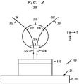
- FIG. 3 shows a block diagram of an optical assembly 300 according to an embodiment.
- Optical assembly 300 comprises a SCOD 100 mounted on device carrier 202 , e.g., as described above in reference to FIGs. 2A-2C .
- Optical assembly 300 further comprises an optical circulator 310 configured to couple light in and/or out of SCOD 100 .
- Optical circulator 310 has three optical ports, which are labeled in FIG. 3 using reference numerals 312 , 314 , and 316 , respectively.
- Port 312 is configured to direct an optical input beam 322 received from an external light source to port 314 .
- Port 314 is configured to direct light of beam 322 toward mirror 130 of SCOD 100 .
- Port 314 is further configured to receive an optical output beam 324 emitted by SCOD 100 through mirror 130 and direct it to port 316 .
- Port 316 is configured to direct light of optical beam 324 to external circuits.
- a lens (not explicitly shown in FIG. 3 ) may be placed between port 314 of optical circulator 310 and mirror 130 of SCOD 100 to improve the optical coupling efficiency and/or reduce optical losses.
- port 314 may comprise a collimator configured to collimate the light thereat.
- optical circulator 310 can be implemented using the fiber-optic circulator Model 6015-3-APC commercially available from Thorlabs, Inc.
- an array of optical circulators 310 may be used to couple light in and out of array 200 ( FIG. 2C ). In such an array, not all of the ports of optical circulators 310 may be used.
- an optical circulator 310 optically coupled to a SCOD 100 configured to operate as a VCSEL may use only ports 314 and 316 to couple the light of output optical beam 324 out of the that SCOD.
- an optical circulator 310 optically coupled to a SCOD 100 configured to operate as a PD may use only ports 312 and 314 to couple the light of input optical beam 322 into that SCOD.
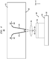
- FIG. 4 shows a block diagram of an optical assembly 400 according to another embodiment.
- Optical assembly 400 comprises a SCOD 100 mounted on device carrier 202 , e.g., as described above in reference to FIGs. 2A-2C .
- Optical assembly 400 further comprises a planar lightwave circuit (PLC) 410 configured to couple light in and/or out of SCOD 100 .
- the main plane of planar lightwave circuit 410 is parallel to the YZ-coordinate plane.
- Circuit 410 comprises optical waveguides 412 and 416 connected to an edge 420 of that circuit as indicated in FIG. 4 . More specifically, the end portions of waveguides 412 and 416 are oriented with respect to edge 420 at an angle that is slightly (e.g., within ⁇ 10 degrees) different from 90 degrees. The ends of waveguides 412 and 416 are separated from one another by a relatively small distance d selected such that both ends are in the field of view of a coupling lens 414 located between edge 420 of circuit 410 and mirror 130 of SCOD 100 .
- lens 414 can be replaced by a suitable set of two or more different lenses configured for optimal light-coupling efficiency for the intended application of circuit 400 .
- lens 414 can be removed, and edge 420 can be positioned to be in very close proximity to (e.g., in direct contact with) mirror 130 .
- waveguide 412 is configured to direct, through lens 414 , an optical input beam 422 received from an external light source toward mirror 130 .
- Waveguide 416 is configured to receive, through lens 414 , an optical output beam 424 emitted by SCOD 100 through mirror 130 and direct it to external circuits.
- Lens 414 is configured to appropriately shape and redirect optical beams 422 and 424 to provide a relatively high optical-coupling efficiency between circuit 410 and SCOD 100 .
- circuit 410 may be used to couple light in and out of array 200 ( FIG. 2C ).
- circuit 410 may have multiple pairs of optical waveguides 412 and 416 (not explicitly shown in FIG. 4 ; see FIG. 5 ) connected to edge 420 . Some of such pairs may be configured to use only one of the two respective waveguides.
- optical waveguides 412 and 416 optically coupled to a SCOD 100 configured to operate as a VCSEL may use only waveguide 416 to couple the light of output optical beam 424 out of the that SCOD.
- optical waveguides 412 and 416 optically coupled to a SCOD 100 configured to operate as a PD may use only waveguide 412 to couple the light of input optical beam 422 into that SCOD.
- circuit 410 may be constructed and operated using waveguide circuits and optical arrangements disclosed, e.g., in U.S. Patent Application Serial No. 15/445,099 , which is incorporated herein by reference in its entirety.
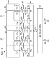
- FIG. 5 shows a block diagram of an optical transceiver 500 according to an embodiment.
- Transceiver 500 comprises: (i) an optical transmitter 502 ; (ii) an optical receiver 504 ; and (iii) an embodiment of SCOD array 200 (also see FIG. 2C ) that includes SCODs 100 1 -100 5 .
- SCODs 100 1 -100 3 are used to implement optical transmitter 502 .
- SCODs 100 4 and 100 5 are used to implement optical receiver 504 .
- Transceiver 500 further comprises an embodiment of planar lightwave circuit 410 (also see FIG. 4 ), an array 520 of lenses 414 1 -414 5 (also see FIG. 4 ), and an electrical circuit 510 operatively connected to SCOD array 200 as indicated in FIG. 5 .
- Waveguide circuit 410 includes fiber connectors 540 and 550 to which external optical fibers can be connected.
- Connector 540 is configured to operate as an optical output port of transceiver 500 .
- Connector 550 is configured to operate as an optical input port of transceiver 500 .
- Electrical circuit 510 is connected to SCOD array 200 using an electrical bus 512 .
- circuit 510 can perform some or all of the following: (i) provide respective bias voltages to SCODs 100 1 -100 5 ; (ii) generate electrical RF drive signals to be applied to some of the SCODs (e.g., SCOD 100 2 ) in response to an electrical analog data-input signal 508 ; and (iii) generate an electrical analog data-output signal 506 in response to the corresponding RF signal(s) received from some of the SCODs (e.g., SCOD 100 4 ).
- SCODs 100 1 -100 5 are configured to operate as a VCSEL, an EAM, a SOA, a PD, and a SOA, respectively. These configurations can be obtained, e.g., as described above in reference to FIGs. 1 and 2 .
- Optical transmitter 502 can operate, for example, as follows.
- SCOD 100 1 generates an optical output beam 424 1 , which is then coupled, by way of lens 414 1 , into waveguide 416 1 of circuit 410 .
- Waveguide 416 1 directs the received light to waveguide 412 2 , which outputs it as an optical output beam 422 2 .
- Lens 414 2 couples beam 422 2 into SCOD 100 2 , where it is modulated to generate a corresponding modulated optical output beam 424 2 .
- the modulation is performed using the electrical RF drive signal generated by circuit 510 in response to the data-input signal 508 , with the drive signal being applied to SCOD 100 2 by way of electrical bus 512 .
- Lens 414 2 couples beam 424 2 into waveguide 416 2 of circuit 410 .
- Waveguide 416 2 directs the received light to waveguide 412 3 , which outputs it as an optical output beam 422 3 .
- Lens 414 3 couples beam 422 3 into SCOD 100 3 , where it is amplified to generate a corresponding amplified optical output beam 424 3 .
- Lens 414 3 then couples beam 424 3 into waveguide 416 3 of circuit 410 .
- waveguide 416 3 directs the received light to connector 540 , where it can be coupled into the optical fiber connected thereto for transmission to a remote receiver (not explicitly shown in FIG. 5 ).
- Optical receiver 504 can operate, for example, as follows.
- Waveguide 412 5 of circuit 410 receives, by way of connector 550 and the optical fiber connected thereto, an optical input signal received from a remote transmitter (not explicitly shown in FIG. 5 ). Waveguide 412 5 then outputs the received light as an optical output beam 422 5 .
- Lens 414 5 couples beam 422 5 into SCOD 100 5 , where it is amplified to generate a corresponding amplified optical output beam 424 5 .
- Lens 414 5 then couples beam 424 5 into waveguide 416 5 of circuit 410 .
- Waveguide 416 5 directs the received light to waveguide 412 4 , which outputs it as an optical output beam 422 4 .
- Lens 414 4 couples beam 422 4 into SCOD 100 4 , where it is converted into a corresponding electrical signal. This electrical signal is then directed by way of electrical bus 512 to circuit 510 , where it is used to generate the data-output signal 506 .
- transceiver 500 Various additional embodiments can be obtained, e.g., using one or more of the following modifications of transceiver 500 .
- SCOD 100 1 can be removed, and waveguide 416 1 can be connected to an external laser (not explicitly shown in FIG. 5 ).
- SCOD 100 3 can be removed, and waveguide 416 2 can be connected to fiber connector 540 instead of waveguide 416 3 .
- SCOD 100 5 can be removed, and waveguide 412 4 can be connected to fiber connector 550 instead of waveguide 412 5 .
- a stand-alone optical receiver can be obtained by removing, disabling, or disconnecting transmitter 502 .
- a stand-alone optical transmitter can be obtained by removing, disabling, or disconnecting receiver 504 .
- circuit 410 shown in FIG. 5 can be replaced by a functionally similar optical circuit constructed using a plurality of appropriately connected optical circulators 310 .
- an apparatus e.g., 500 , FIG. 5
- a plurality of optical devices e.g., 100 1 -100 5 , FIG. 5
- a planar surface e.g., 214 , FIG.
- each of the optical devices being configured to receive light, emit light, or receive and emit light substantially (e.g., within ⁇ 10 degrees) orthogonally to the planar surface;
- the plurality of optical devices include a first optical device and a second optical device; wherein the first optical device is configured to operate as an optical device of a first type; wherein the second optical device is configured to operate as an optical device of a second type different from the first type; and wherein the first type and the second type are selected from a device-type set consisting of a laser (e.g., VCSEL , FIG. 5 ), an optical amplifier (e.g., SOA , FIG. 5 ), a reflective optical modulator (e.g., EAM , FIG. 5 ), and a photodetector (e.g., PD , FIG. 5 ).
- a laser e.g., VCSEL , FIG. 5
- an optical amplifier e.g., SOA , FIG. 5
- the plurality of optical devices include a third optical device configured to operate as an optical device of a third type different from the first type and the second type and selected from said device-type set.
- the plurality of optical devices include a fourth optical device configured to operate as an optical device of a fourth type different from the first, second, and third types and selected from said device-type set.
- the plurality of optical devices include a third optical device configured to operate as an optical device of the second type (e.g., SOA and SOA , FIG. 5 ).
- a third optical device configured to operate as an optical device of the second type (e.g., SOA and SOA , FIG. 5 ).
- each of the optical devices comprises a respective semiconductor diode (e.g., 110/112/118 , FIG. 1 ) that includes a respective multiple-quantum-well structure (e.g., 112 , FIG. 1 ).
- each of the respective semiconductor diodes comprises a respective plurality of thin semiconductor layers (e.g., 110/112/114/116/118 , FIG. 1 ) oriented substantially (e.g., within ⁇ 10 degrees) parallel to the planar surface.
- the apparatus further comprises an electrical circuit (e.g., 510 , FIG. 5 ) connected to electrically bias the respective semiconductor diodes.
- an electrical circuit e.g., 510 , FIG. 5
- the electrical circuit is configured to apply: a forward bias to the semiconductor diode of the first optical device; and a reverse bias to the semiconductor diode of the second optical device.
- the apparatus further comprises a device carrier (e.g., 202 , FIGs. 2C , 5 ) that comprises the planar surface, the device carrier being configured to electrically connect the optical devices to the electrical circuit.
- a device carrier e.g., 202 , FIGs. 2C , 5
- the device carrier being configured to electrically connect the optical devices to the electrical circuit.
- each of the optical devices comprises a respective optical resonator bounded by a respective first optical reflector (e.g., 106 , FIG. 1 ) and a respective second optical reflector (e.g., 130 , FIG. 1 ), the first optical reflector being a nontransparent optical reflector and the second optical reflector being a partially transparent dielectric optical reflector.
- the first and second optical devices have nominally identical first optical reflectors, each being a metal mirror.
- the second optical reflector of the first optical device differs from the second optical reflector of the second optical device in at least one of: reflectivity, transmissivity, chemical composition, and thickness.
- each of the respective optical resonators comprises a respective semiconductor diode (e.g., 110/112/118 , FIG. 1 ) that includes a respective multiple-quantum-well structure (e.g., 112 , FIG. 1 ).
- the apparatus further comprises an optical circuit (e.g., 410 , FIG. 5 ; or functional equivalent thereof constructed using 310 , FIG. 3 ) configured to optically couple the first optical device and the second optical device such that light emitted by the first optical device is received by the second optical device.
- an optical circuit e.g., 410 , FIG. 5 ; or functional equivalent thereof constructed using 310 , FIG. 3
- the first optical device is configured to operate as a laser (e.g., 100 1 , FIG. 5 ); and wherein the second optical device is configured to operate as an optical modulator (e.g., 100 2 , FIG. 5 ).
- the first optical device is configured to operate as an optical modulator (e.g., 100 2 , FIG. 5 ); and wherein the second optical device is configured to operate as an optical amplifier (e.g., 100 3 , FIG. 5 ).
- the first optical device is configured to operate as an optical amplifier (e.g., 100 5 , FIG. 5 ); and wherein the second optical device is configured to operate as a photodetector (e.g., 100 4 , FIG. 5 ).
- the optical circuit comprises a planar lightwave circuit (e.g., 410 , FIGs. 4 , 5 ).
- the optical circuit comprises an optical circulator (e.g., 310 , FIG. 3 ).
- the apparatus further comprises an optical data transmitter (e.g., 502 , FIG. 5 ) that includes the first and second optical devices.
- an optical data transmitter e.g., 502 , FIG. 5
- the apparatus further comprises an optical data receiver (e.g., 504 , FIG. 5 ) that includes the first and second optical devices.
- an optical data receiver e.g., 504 , FIG. 5
- the apparatus further comprises an optical data transceiver (e.g., 500 , FIG. 5 ) that includes the first and second optical devices.
- an optical data transceiver e.g., 500 , FIG. 5
- Couple refers to any manner known in the art or later developed in which energy is allowed to be transferred between two or more elements, and the interposition of one or more additional elements is contemplated, although not required. Conversely, the terms “directly coupled,” “directly connected,” etc., imply the absence of such additional elements.
- circuitry may refer to one or more or all of the following: (a) hardware-only circuit implementations (such as implementations in only analog and/or digital circuitry); (b) combinations of hardware circuits and software, such as (as applicable): (i) a combination of analog and/or digital hardware circuit(s) with software/firmware and (ii) any portions of hardware processor(s) with software (including digital signal processor(s)), software, and memory(ies) that work together to cause an apparatus, such as a mobile phone or server, to perform various functions); and (c) hardware circuit(s) and or processor(s), such as a microprocessor(s) or a portion of a microprocessor(s), that requires software (e.g., firmware) for operation, but the software may not be present when it is not needed for operation.”
- This definition of circuitry applies to all uses of this term in this application, including in any claims.
- circuitry also covers an implementation of merely a hardware circuit or processor (or multiple processors) or portion of a hardware circuit or processor and its (or their) accompanying software and/or firmware.
- circuitry also covers, for example and if applicable to the particular claim element, a baseband integrated circuit or processor integrated circuit for a mobile device or a similar integrated circuit in server, a cellular network device, or other computing or network device.
Landscapes
- Physics & Mathematics (AREA)
- Electromagnetism (AREA)
- Engineering & Computer Science (AREA)
- Computer Networks & Wireless Communication (AREA)
- Signal Processing (AREA)
- Optics & Photonics (AREA)
- Condensed Matter Physics & Semiconductors (AREA)
- General Physics & Mathematics (AREA)
- Computing Systems (AREA)
- Semiconductor Lasers (AREA)
Abstract
Description
- Various example embodiments relate to optical communication equipment and, more specifically but not exclusively, to optical transmitters and receivers.
- This section introduces aspects that may help facilitate a better understanding of the disclosure. Accordingly, the statements of this section are to be read in this light and are not to be understood as admissions about what is in the prior art or what is not in the prior art.
- An optical transceiver may include one or more of the following optical devices: (i) an electrically driven light source, such as a laser diode; (ii) an optical amplifier; (iii) an optical-to-electrical converter, such as a photodiode; and (iv) an optoelectronic component that can control propagation and/or certain properties of light, such as an optical modulator or an optical switch. The optical transceiver may additionally include one or more electronic components that enable the use of these and possibly other optical devices in a manner consistent with the intended function or application. Different integration and packaging technologies may be used to combine various optical devices and the corresponding electronic components into a functional, practically useful integrated circuit, package, card, and/or assembly. Such technologies continue to expand and evolve, e.g., through the development of new solutions for the emerging products and applications.
- Disclosed herein are various embodiments of optical transmitters, receivers, and transceivers implemented using a plurality of surface-coupled optical devices that can be manufactured on the same planar substrate and then post-processed to provide some of the devices with different respective partially transparent front mirrors compatible with and/or customized for different respective optical functions. When appropriately electrically biased and driven, different subsets of such devices can operate as lasers, optical modulators, optical amplifiers, and photodetectors, respectively. In this manner, an integrated array of such devices can be customized to provide the optical functions needed for the intended end product. For example, an optical transmitter can be constructed using an integrated array that comprises three surface-coupled optical devices configured to operate as a laser, an optical modulator, and an optical amplifier, respectively. An optical receiver can be constructed using an integrated array that comprises two surface-coupled optical devices configured to operate as an optical amplifier and a photodetector, respectively.
- Advantageously, the use of integrated arrays of such surface-coupled optical devices can help to streamline the system design, simplify the system integration/packaging, and/or reduce the system development and production costs.
- According to an example embodiment, provided is an apparatus comprising a plurality of optical devices supported on a planar surface, each of the optical devices being configured to receive light, emit light, or receive and emit light substantially orthogonally to the planar surface; wherein the plurality of optical devices includes a first optical device and a second optical device; wherein the first optical device is configured to operate as an optical device of a first type; wherein the second optical device is configured to operate as an optical device of a second type different from the first type; and wherein the first type and the second type are selected from a device-type set consisting of a vertical-cavity surface-emitting laser, a semiconductor optical amplifier, a reflective optical modulator, and a photodetector.
- Other aspects, features, and benefits of various disclosed embodiments will become more fully apparent, by way of example, from the following detailed description and the accompanying drawings, in which:
-
FIG. 1 shows a schematic cross-sectional side view of a surface-coupled optical device (SCOD) according to an embodiment; -
FIGs. 2A-2C pictorially illustrate a manufacturing method that can be used to make an array of SCODs ofFIG. 1 according to an embodiment; -
FIG. 3 shows a block diagram of an optical assembly that includes a SCOD ofFIG. 1 according to an embodiment; -
FIG. 4 shows a block diagram of an optical assembly that includes a SCOD ofFIG. 1 according to another embodiment; and -
FIG. 5 shows a block diagram of an optical transceiver that includes an array of SCODs ofFIG. 1 according to an embodiment. - Some embodiments of the present application may be able to use some features, apparatus, and/or methods disclosed in one or more of the below-listed and concurrently filed, U.S. applications:
- U.S. Patent Application No. __/__________, titled "OPTICAL TRANSMITTER HAVING AN ARRAY OF SURFACE-COUPLED ELECTRO-ABSORPTION MODULATORS", by Mark Earnshaw and Stefano Grillanda, Nokia Docket No. 105324-US-NP;
- U.S. Patent Application No. __/__________, titled "CHIP-IN-CONNECTOR PHOTONIC APPARATUS", by Yee Low and Nagesh Basavanhally, Nokia Docket No. 104727-US-NP;
- U.S. Provisional Patent Application No. __/__________, titled "REFLECTIVE OPTICAL DATA MODULATOR", by David Neilson, Nokia Docket No. 105420-US-PSP; and
- U.S. Provisional Patent Application No. __/__________, titled "OPTICAL COMMUNICATION WITH WAVELENGTH-DEPENDENT AMPLITUDE PRE-COMPENSATION", by Mark Earnshaw, Nokia Docket
No. 105431-US-PSP. -
FIG. 1 shows a schematic cross-sectional side view of a surface-coupled optical device (SCOD) 100 according to an embodiment. Depending on the electrical configuration,SCOD 100 can be operated as a vertical-cavity surface-emitting laser (VCSEL), a semiconductor optical amplifier (SOA), an electro-absorption modulator (EAM), or a photodetector (PD). The different electrical configurations corresponding to these four different optical functions ofSCOD 100 are described in more detail below. - In some embodiments, the same physical instance of
SCOD 100 can be reconfigurable, e.g., by changing the electrical configuration thereof, to provide any selected one of the four above-mentioned optical functions or any selected one of a subset of the four optical functions. In such embodiments, the optical function of thatparticular SCOD 100 can be changed, e.g., by changing the electrical configuration thereof, such as the bias voltage and/or the bias-voltage polarity applied thereto. - In some other embodiments, SCOD 100 can be designed to perform a selected one of the four optical functions, e.g., by having certain physical characteristics that are beneficial for and/or geared towards that particular optical function. In some of such embodiments, that
particular SCOD 100 may not be able to perform at least some of the other three optical functions even if placed into a corresponding electrical configuration. -
SCOD 100 is "surface-coupled" in the sense that, in operation, this device receives and/or emits a light beam in a direction that is substantially orthogonal to the main plane of the device, which is parallel to the XY-coordinate plane of the XYZ triad shown inFIG. 1 . The XY-coordinate plane typically corresponds to the main plane of the planar substrate on which the layered structure ofSCOD 100 has been formed during fabrication (see, e.g.,FIGs. 2A-2C ). Due to this geometry, a large number ofSCODs 100 can be manufactured on a single substrate (e.g., a semiconductor wafer). - SCOD 100 includes a plurality of layers that are substantially parallel to the XY-coordinate plane. The direction orthogonal to those layers (i.e., parallel to the Z-coordinate axis) may hereafter be referred to as the vertical or surface-normal direction. The directions parallel to those layers may hereafter be referred to as the horizontal or lateral directions. Some of the layers may include two or more sub-layers (not explicitly shown in
FIG. 1 ) that differ from each other in chemical composition and/or the concentration and type of the introduced dopant(s). SCOD 100 also includesmetal electrodes 102 and 1041-1042 electrically connected to some of the layers as described in more detail below. In an example embodiment, the vertical size (or thickness) ofSCOD 100 is significantly smaller than its lateral size (e.g., depth and/or width). - In some embodiments, metal electrodes 1041-1042 can be electrically connected to one another by being parts of the same electrode having, e.g., an O-shape in the top view thereof (e.g., if viewed along the Z-coordinate axis).
- SCOD 100 comprises an optical resonator defined by
mirrors - In an example embodiment,
mirror 106 is a metal (e.g., gold or gold-plated) mirror having relatively high (e.g., >99%) reflectivity at the nominal operating wavelength at the side of the mirror facing down (in the projection shown inFIG. 1 ). Mirror 106 is typically such that it does not allow any light to pass therethrough. As a result, the shown embodiment ofSCOD 100 can typically be used only in an optical configuration that does not require light to be transmitted through the SCOD, e.g., in reflection. - In some alternative embodiments,
mirror 106 can be replaced by a suitable distributed Bragg reflector (DBR) mirror. As known in the pertinent art, a DBR mirror can be formed, e.g., using a stack of semiconductor or dielectric layers, each having a quarter-wavelength thickness, with adjacent layers of the stack having alternating refractive indices. In such embodiments, SCOD 100 may be used in transmission. - In an example embodiment,
mirror 130 is a partially transparent dielectric mirror that enables light of the nominal operating wavelength to be properly coupled into and/or out of the optical resonator. For illustration purposes and without any implied limitations,FIG. 1 shows an embodiment in whichmirror 130 comprises four dielectric layers 1321-1324 . In an alternative embodiment,mirror 130 can be implemented using a different (from four) number of constituent dielectric layers. - In some embodiments, layers 1321 and 1323 comprise silicon dioxide, and layers 1323 and 1324 comprise silicon nitride. In an alternative embodiment,
mirror 130 can be implemented using dielectric layers of other suitable chemical composition. - In some embodiments,
mirror 130 can be replaced by a suitable DBR mirror made of semiconductor materials. - The optical resonator defined by
mirrors type semiconductor layers 108 and 110, n-type semiconductor layers thin layers layers Layer 108 may have a higher dopant concentration than layer 110, such thatlayers 108 and 110 can be referred to as p+ and p layers, respectively.Layer 120 may similarly have a higher dopant concentration thanlayer 118, such thatlayers - In some embodiments, MQW structure 112 may comprise quantum dots (not explicitly shown in
FIG. 1 ), each quantum dot being respective quantum well. In some embodiments, quantum dots may be used in addition to or instead of the layer-type quantum wells shown inFIG. 1 . - In the embodiment shown in
FIG. 1 , the optical resonator defined bymirrors optional dielectric layer 105 located betweenmirror 106 andsemiconductor layer 108. In an example embodiment, this layer comprises SiO2 or Si3N4. In an alternative embodiment,layer 105 can be absent. - A person of ordinary skill in the art will understand that the choices of (i) the semiconductor materials for
layers mirrors SCOD 100. For example, different telecommunications applications may use different embodiments ofSCOD 100 designed for the spectral bands located near 850 nm, 1300 nm, and 1550 nm, respectively. - In some embodiments,
SCOD 100 may include additional layers (not explicitly shown inFIG. 1 ) located betweenlayers 120 and 1321 . An example of such layers can be one or more etch-stop layers and one or more buffer layers used in the manufacturing process, e.g., as explained below in reference toFIGs. 2A-2C . - In an example embodiment, the following semiconductor materials can be used to implement SCOD 100: (i) Zn-doped In(x)Ga(1-x-y)Al(y)As for
layer 108; (ii) Zn-doped In(x)Al(1-x)As for layer 110; (iii) In(x)Ga(1-x)As forlayers 114; (iv) In(x)Al(1-x)As forlayers 116; (v) Si-doped In(x)Al(1-x)As forlayer 118; and (vi) Si-doped In(x)Ga(1-x-y)Al(y)As forlayer 120. In alternative embodiments, other semiconductor materials and dopants can also be used. - In an example embodiment, layers 110 and 118 and MQW structure 112 form a p-i-n diode (also sometimes referred to as a "PIN diode") that can be electrically biased using
electrodes 102 and 104. Ohmic contact betweenelectrode 102 and layer 110 can be created usingmetal contact pads 107 andlayer 108 as known in the art. Ohmic contact between electrode(s) 104 andlayer 118 can be created usingmetal contact pads 117 and an additional thin n+ or n++ semiconductor layer (not explicitly shown inFIG. 1 ) located betweencontact pads 117 andlayer 118. - To operate
SCOD 100 as a VCSEL,electrodes 102 and 104 can be electrically connected to apply an appropriate forward bias to PIN diode 110/112/118. - As used herein, the term "forward bias" refers to an electrical configuration of a semiconductor-junction diode in which the n-type material is at a low potential, and the p-type material is at a high potential. If the forward bias is greater than the intrinsic voltage drop Vpn across the corresponding p-i-n junction, then the corresponding potential barrier can be overcome by the electrical carriers, and a relatively large forward current can flow through the junction. For example, for silicon-based diodes the value of Vpn is approximately 0.7 V. For germanium-based diodes, the value of Vpn is approximately 0.3 V, etc.
- When PIN diode 110/112/118 is appropriately forward-biased, a relatively large injection current flows through MQW structure 112, thereby causing the MQW structure to generate light that is then amplified due to the multiple passes therethrough caused by light oscillation in the optical resonator between
mirrors SCOD 100 throughmirror 130, thereby generating an output light beam. A person of ordinary skill in the art will understand that to enable the VCSEL function,SCOD 100 needs to be capable of a relatively high optical gain, which can be achieved, in part, by properly selecting the materials and structure ofmirror 130. - To operate
SCOD 100 as an SOA,electrodes 102 and 104 can be electrically connected to apply an appropriate forward bias to PIN diode 110/112/118, which forward bias may be different from that used in the above-described VCSEL configuration. More specifically, in the SOA configuration, the gain provided by the optical resonator ofSCOD 100 is typically below the lasing threshold, but is nevertheless sufficient for generating new light, through stimulated emission, in response to an external light beam coupled into the optical resonator throughmirror 130. The corresponding value of the optical gain can be achieved, in part, by properly selecting the materials and structure ofmirror 130. In some embodiments, the materials and structure ofmirror 130 selected to provide a desired SOA function ofSCOD 100 may be different from those used to provide the above-described VCSEL function. - To operate
SCOD 100 as an EAM,electrodes 102 and 104 can be electrically connected to apply to PIN diode 110/112/118 a combination of an appropriate reverse bias and a driving radio-frequency (RF) signal. - As used herein, the term "reverse bias" refers to an electrical configuration of a semiconductor-junction diode in which the n-type material is at a high electrical potential, and the p-type material is at a low electrical potential. The reverse bias typically causes the depletion layer to grow wider due to a lack of electrons and/or holes, which presents a high impedance path across the junction and substantially prevents a current flow therethrough. However, a very small reverse leakage current can still flow through the junction in the reverse-bias configuration.
- The principle of operation of
SCOD 100 in the EAM configuration is based on the so-called quantum-confined Stark effect (QCSE) due to which the optical absorption near the effective band edge of MQW structure 112 depends on the applied electric field. More specifically, the reverse bias applied to the PIN diode 110/112/118 causes MQW structure 112 to be subjected to an electric field of certain strength. During the positive swing of the driving RF signal, the electric-field strength increases, thereby red-shifting the band edge. During the negative swing of the driving RF signal, the electric-field strength decreases, thereby blue-shifting the band edge. These band-edge shifts change the light transmittance of MQW structure 112 at the carrier wavelength, thereby modulating the intensity of light that oscillates in the optical resonator betweenmirrors mirror 130. - A person of ordinary skill in the art will understand that an optimized EAM function of
SCOD 100 may be facilitated, at least in part, by a corresponding (e.g., different from any of the above-described) selection of the materials and structure ofmirror 130. - To operate
SCOD 100 as a PD,electrodes 102 and 104 can be electrically connected to apply to PIN diode 110/112/118 an appropriate dc reverse bias, which may be different from (e.g., larger than) that used in the above-described EAM configuration. The reverse bias creates a relatively large electric field across the p-i-n junction that can separate the electrical carriers (e.g., holes and electrons) generated therein by the absorbed light coupled into the optical resonator ofSCOD 100 throughmirror 130. The separated electrical carriers generate a photocurrent that can be collected and measured as known in the art to determine the light intensity. - A person of ordinary skill in the art will understand that an optimized PD function of
SCOD 100 may be facilitated, at least in part, by a corresponding (e.g., different from any of the above-described) selection of the materials and structure ofmirror 130. - The lateral dimensions of the optical resonator in
SCOD 100 can be defined using an external aperture (not explicitly shown inFIG. 1 ) and/or ion-implantedregions 124. Ion-implantedregions 124 can be formed by implanting suitable ions (e.g., the hydrogen ions, H+) into MQW structure 112 around its periphery, e.g., as indicated inFIG. 1 . The ion-implantation process disrupts, perturbs, and/or destroys the semiconductor lattice inregions 124, thereby inhibiting the flow of electrical current(s) therethrough and/or hindering the physical processes therein that are pertinent to the above-described optical functions ofSCOD 100. In an example embodiment, the middle portion of MQW structure 112 laterally bounded byregions 124 may have an approximately circular cross-sectional shape in a plane parallel to the XY-coordinate plane. In alternative embodiments, other cross-sectional geometric shapes are also possible. - Encapsulating and/or filler materials can be used as known in the pertinent art to cover and/or fill the gaps (if any) between the various layers, structures, and electrodes of
SCOD 100, thereby providing a substantially monolithic and mechanically robust overall device structure. - One beneficial optical characteristic of
SCOD 100 is that its operation, in various above-described configurations, can be substantially polarization-independent due to the surface-coupled nature of the device. For comparison, waveguide-based semiconductor optical devices (e.g., lasers, amplifiers, modulators, and photodetectors) can typically be polarization-dependent, e.g., due to a relatively large difference in the group indices (i.e., effective refractive indices) of the transverse electric (TE) and transverse magnetic (TM) polarizations in the corresponding optical waveguides. This particular characteristic can make it relatively difficult to construct a polarization-diverse waveguide-based semiconductor optical device having a substantially polarization-independent response and/or capable of appropriately handling polarization-division-multiplexed (PDM) signals. Advantageously, the latter problem can be significantly alleviated or avoided altogether with the use of various embodiments ofSCOD 100. -
FIGs. 2A-2C pictorially illustrate a manufacturing method that can be used to make anarray 200 ofSCODs 100 according to an embodiment. -
FIG. 2C shows a schematic cross-sectional side view ofarray 200. For illustration purposes and without any implied limitations,FIG. 2C shows an embodiment in whicharray 200 comprises fourSCODs 100, which are labeled 1001-1004. In an alternative embodiment,array 200 may have a different (from four) number ofSCODs 100. - SCODs 1001-1004 are supported on and electrically and mechanically connected to a
device carrier 202 usingsolder bumps 210 attached toelectrodes 102, 104 (also seeFIG. 1 ). The orientation of SCODs 1001-1004 is such that mirrors 130 are facing away from asurface 214 ofdevice carrier 202, on which the SCODs are mounted. Electrical connections between each of SCODs 1001-1004 and the corresponding external electrical circuit(s) (such as,circuit 510,FIG. 5 ) can be provided by patterned conducting (such as metal) layers located within the body and/or onsurface 214 ofdevice carrier 202. In various embodiments,device carrier 202 can be implemented using any one or any suitable combination of the following: one or more substrates, one or more redistribution layers (RDLs), one or more interposers, one or more laminate plates, and one or more circuit sub-mounts, etc. - In some embodiments, SCODs 1001-1004 can be nominally identical.
- In some other embodiments, SCODs 1001-1004 may have nominally identical portions 128 (also see
FIG. 1 ), but different respective mirrors 1301-1304. In such embodiments, some of mirrors 1301-1304 may differ from some of the other mirrors, e.g., in reflectivity/transmissivity, thickness, the number of constituent layers 132 (seeFIG. 1 ), and/or the chemical composition of at least some of those constituent layers. - In some embodiments, different subsets of SCODs 1001-1004 may be specifically designed and configured to perform different respective optical functions selected from the above-described VCSEL, SOA, EAM, and PD functions. In different ones of such embodiments, the number of such subsets can be two, three, or four.
-
Array 200 ofFIG. 2C can be fabricated by first forming a corresponding array 201 ofportions 128 on asuitable substrate 204 as illustrated inFIG. 2A . In an example embodiment,substrate 204 can be an InP substrate.Portions 128 can be formed onsubstrate 204 in a conventional manner, e.g., using a multistep fabrication process comprising at least some of the following: photolithography, ion implantation, dry and/or wet etching, thermal treatments and anneals, oxidation, chemical and physical vapor deposition, epitaxial growth, electrochemical deposition, and chemical-mechanical planarization. - In the next fabrication step, array 201 is flip-chip bonded to
device carrier 202 using solder bumps 210. After the flip-chip bonding,substrate 204 is removed, e.g., by reactive etching, thereby exposinglayers 120 of portions 128 (e.g., as indicated inFIG. 2B ) or the corresponding etch-stop layers (not explicitly shown inFIG. 2 ). Mirrors 1301-1304 are then formed on the exposed top surfaces of the resulting circuit 203 (FIG. 2B ), thereby converting the latter into array 200 (FIG. 2C ). -
FIG. 3 shows a block diagram of anoptical assembly 300 according to an embodiment.Optical assembly 300 comprises aSCOD 100 mounted ondevice carrier 202, e.g., as described above in reference toFIGs. 2A-2C .Optical assembly 300 further comprises anoptical circulator 310 configured to couple light in and/or out ofSCOD 100. -
Optical circulator 310 has three optical ports, which are labeled inFIG. 3 usingreference numerals Port 312 is configured to direct anoptical input beam 322 received from an external light source toport 314.Port 314 is configured to direct light ofbeam 322 towardmirror 130 ofSCOD 100.Port 314 is further configured to receive anoptical output beam 324 emitted bySCOD 100 throughmirror 130 and direct it toport 316.Port 316 is configured to direct light ofoptical beam 324 to external circuits. - In some embodiments, a lens (not explicitly shown in
FIG. 3 ) may be placed betweenport 314 ofoptical circulator 310 andmirror 130 ofSCOD 100 to improve the optical coupling efficiency and/or reduce optical losses. - In some embodiments,
port 314 may comprise a collimator configured to collimate the light thereat. - In some embodiments,
optical circulator 310 can be implemented using the fiber-optic circulator Model 6015-3-APC commercially available from Thorlabs, Inc. - In some embodiments, an array of
optical circulators 310 may be used to couple light in and out of array 200 (FIG. 2C ). In such an array, not all of the ports ofoptical circulators 310 may be used. For example, anoptical circulator 310 optically coupled to aSCOD 100 configured to operate as a VCSEL may useonly ports optical beam 324 out of the that SCOD. As another example, anoptical circulator 310 optically coupled to aSCOD 100 configured to operate as a PD may useonly ports optical beam 322 into that SCOD. -
FIG. 4 shows a block diagram of an optical assembly 400 according to another embodiment. Optical assembly 400 comprises aSCOD 100 mounted ondevice carrier 202, e.g., as described above in reference toFIGs. 2A-2C . Optical assembly 400 further comprises a planar lightwave circuit (PLC) 410 configured to couple light in and/or out ofSCOD 100. The main plane ofplanar lightwave circuit 410 is parallel to the YZ-coordinate plane. -
Circuit 410 comprisesoptical waveguides edge 420 of that circuit as indicated inFIG. 4 . More specifically, the end portions ofwaveguides waveguides coupling lens 414 located betweenedge 420 ofcircuit 410 andmirror 130 ofSCOD 100. - In some alternative embodiments,
lens 414 can be replaced by a suitable set of two or more different lenses configured for optimal light-coupling efficiency for the intended application of circuit 400. - In some other alternative embodiments,
lens 414 can be removed, and edge 420 can be positioned to be in very close proximity to (e.g., in direct contact with)mirror 130. - In the shown embodiment,
waveguide 412 is configured to direct, throughlens 414, anoptical input beam 422 received from an external light source towardmirror 130.Waveguide 416 is configured to receive, throughlens 414, anoptical output beam 424 emitted bySCOD 100 throughmirror 130 and direct it to external circuits.Lens 414 is configured to appropriately shape and redirectoptical beams circuit 410 andSCOD 100. - In some embodiments,
circuit 410 may be used to couple light in and out of array 200 (FIG. 2C ). In such embodiments,circuit 410 may have multiple pairs ofoptical waveguides 412 and 416 (not explicitly shown inFIG. 4 ; seeFIG. 5 ) connected to edge 420. Some of such pairs may be configured to use only one of the two respective waveguides. For example,optical waveguides SCOD 100 configured to operate as a VCSEL may use only waveguide 416 to couple the light of outputoptical beam 424 out of the that SCOD. As another example,optical waveguides SCOD 100 configured to operate as a PD may use only waveguide 412 to couple the light of inputoptical beam 422 into that SCOD. - Additional embodiments of
circuit 410 may be constructed and operated using waveguide circuits and optical arrangements disclosed, e.g., inU.S. Patent Application Serial No. 15/445,099 , which is incorporated herein by reference in its entirety. -
FIG. 5 shows a block diagram of an optical transceiver 500 according to an embodiment. Transceiver 500 comprises: (i) anoptical transmitter 502; (ii) anoptical receiver 504; and (iii) an embodiment of SCOD array 200 (also seeFIG. 2C ) that includes SCODs 1001-1005. SCODs 1001-1003 are used to implementoptical transmitter 502.SCODs optical receiver 504. - Transceiver 500 further comprises an embodiment of planar lightwave circuit 410 (also see
FIG. 4 ), anarray 520 of lenses 4141-4145 (also seeFIG. 4 ), and anelectrical circuit 510 operatively connected toSCOD array 200 as indicated inFIG. 5 . -
Waveguide circuit 410 includesfiber connectors Connector 540 is configured to operate as an optical output port of transceiver 500.Connector 550 is configured to operate as an optical input port of transceiver 500. -
Electrical circuit 510 is connected toSCOD array 200 using anelectrical bus 512. In operation,circuit 510 can perform some or all of the following: (i) provide respective bias voltages to SCODs 1001-1005; (ii) generate electrical RF drive signals to be applied to some of the SCODs (e.g., SCOD 1002 ) in response to an electrical analog data-input signal 508; and (iii) generate an electrical analog data-output signal 506 in response to the corresponding RF signal(s) received from some of the SCODs (e.g., SCOD 1004 ). - In the shown embodiment, SCODs 1001-1005 are configured to operate as a VCSEL, an EAM, a SOA, a PD, and a SOA, respectively. These configurations can be obtained, e.g., as described above in reference to
FIGs. 1 and2 . -
Optical transmitter 502 can operate, for example, as follows. -
SCOD 1001 generates anoptical output beam 4241 , which is then coupled, by way oflens 4141 , intowaveguide 4161 ofcircuit 410.Waveguide 4161 directs the received light towaveguide 4122 , which outputs it as anoptical output beam 4222 .Lens 4142couples beam 4222 intoSCOD 1002 , where it is modulated to generate a corresponding modulatedoptical output beam 4242 . The modulation is performed using the electrical RF drive signal generated bycircuit 510 in response to the data-input signal 508, with the drive signal being applied to SCOD 1002 by way ofelectrical bus 512.Lens 4142couples beam 4242 intowaveguide 4162 ofcircuit 410.Waveguide 4162 directs the received light towaveguide 4123 , which outputs it as anoptical output beam 4223 .Lens 4143couples beam 4223 intoSCOD 1003 , where it is amplified to generate a corresponding amplifiedoptical output beam 4243 .Lens 4143 then couplesbeam 4243 intowaveguide 4163 ofcircuit 410. Finally,waveguide 4163 directs the received light toconnector 540, where it can be coupled into the optical fiber connected thereto for transmission to a remote receiver (not explicitly shown inFIG. 5 ). -
Optical receiver 504 can operate, for example, as follows. -
Waveguide 4125 ofcircuit 410 receives, by way ofconnector 550 and the optical fiber connected thereto, an optical input signal received from a remote transmitter (not explicitly shown inFIG. 5 ).Waveguide 4125 then outputs the received light as anoptical output beam 4225 .Lens 4145couples beam 4225 intoSCOD 1005 , where it is amplified to generate a corresponding amplifiedoptical output beam 4245 .Lens 4145 then couplesbeam 4245 intowaveguide 4165 ofcircuit 410.Waveguide 4165 directs the received light towaveguide 4124 , which outputs it as anoptical output beam 4224 .Lens 4144couples beam 4224 intoSCOD 1004 , where it is converted into a corresponding electrical signal. This electrical signal is then directed by way ofelectrical bus 512 tocircuit 510, where it is used to generate the data-output signal 506. - Various additional embodiments can be obtained, e.g., using one or more of the following modifications of transceiver 500.
-
SCOD 1001 can be removed, andwaveguide 4161 can be connected to an external laser (not explicitly shown inFIG. 5 ). -
SCOD 1003 can be removed, andwaveguide 4162 can be connected tofiber connector 540 instead ofwaveguide 4163 . -
SCOD 1005 can be removed, andwaveguide 4124 can be connected tofiber connector 550 instead ofwaveguide 4125 . - A stand-alone optical receiver can be obtained by removing, disabling, or disconnecting
transmitter 502. - A stand-alone optical transmitter can be obtained by removing, disabling, or disconnecting
receiver 504. - In some embodiments, the embodiment of
circuit 410 shown inFIG. 5 can be replaced by a functionally similar optical circuit constructed using a plurality of appropriately connectedoptical circulators 310. - According to an example embodiment disclosed above, e.g., in the summary section and/or in reference to any one or any combination of some or all of
FIGs. 1-5 , provided is an apparatus (e.g., 500,FIG. 5 ) comprising: a plurality of optical devices (e.g., 1001-1005 ,FIG. 5 ) supported on a planar surface (e.g., 214,FIG. 2C ), each of the optical devices being configured to receive light, emit light, or receive and emit light substantially (e.g., within ±10 degrees) orthogonally to the planar surface; wherein the plurality of optical devices include a first optical device and a second optical device; wherein the first optical device is configured to operate as an optical device of a first type; wherein the second optical device is configured to operate as an optical device of a second type different from the first type; and wherein the first type and the second type are selected from a device-type set consisting of a laser (e.g., VCSEL,FIG. 5 ), an optical amplifier (e.g., SOA,FIG. 5 ), a reflective optical modulator (e.g., EAM,FIG. 5 ), and a photodetector (e.g., PD,FIG. 5 ). - In some embodiments of the above apparatus, the plurality of optical devices include a third optical device configured to operate as an optical device of a third type different from the first type and the second type and selected from said device-type set.
- In some embodiments of any of the above apparatus, the plurality of optical devices include a fourth optical device configured to operate as an optical device of a fourth type different from the first, second, and third types and selected from said device-type set.
- In some embodiments of any of the above apparatus, the plurality of optical devices include a third optical device configured to operate as an optical device of the second type (e.g., SOA and SOA,
FIG. 5 ). - In some embodiments of any of the above apparatus, each of the optical devices comprises a respective semiconductor diode (e.g., 110/112/118,
FIG. 1 ) that includes a respective multiple-quantum-well structure (e.g., 112,FIG. 1 ). - In some embodiments of any of the above apparatus, each of the respective semiconductor diodes comprises a respective plurality of thin semiconductor layers (e.g., 110/112/114/116/118,
FIG. 1 ) oriented substantially (e.g., within ±10 degrees) parallel to the planar surface. - In some embodiments of any of the above apparatus, the apparatus further comprises an electrical circuit (e.g., 510,
FIG. 5 ) connected to electrically bias the respective semiconductor diodes. - In some embodiments of any of the above apparatus, the electrical circuit is configured to apply: a forward bias to the semiconductor diode of the first optical device; and a reverse bias to the semiconductor diode of the second optical device.
- In some embodiments of any of the above apparatus, the apparatus further comprises a device carrier (e.g., 202,
FIGs. 2C ,5 ) that comprises the planar surface, the device carrier being configured to electrically connect the optical devices to the electrical circuit. - In some embodiments of any of the above apparatus, each of the optical devices comprises a respective optical resonator bounded by a respective first optical reflector (e.g., 106,
FIG. 1 ) and a respective second optical reflector (e.g., 130,FIG. 1 ), the first optical reflector being a nontransparent optical reflector and the second optical reflector being a partially transparent dielectric optical reflector. - In some embodiments of any of the above apparatus, the first and second optical devices have nominally identical first optical reflectors, each being a metal mirror.
- In some embodiments of any of the above apparatus, the second optical reflector of the first optical device differs from the second optical reflector of the second optical device in at least one of: reflectivity, transmissivity, chemical composition, and thickness.
- In some embodiments of any of the above apparatus, each of the respective optical resonators comprises a respective semiconductor diode (e.g., 110/112/118,
FIG. 1 ) that includes a respective multiple-quantum-well structure (e.g., 112,FIG. 1 ). - In some embodiments of any of the above apparatus, the apparatus further comprises an optical circuit (e.g., 410,
FIG. 5 ; or functional equivalent thereof constructed using 310,FIG. 3 ) configured to optically couple the first optical device and the second optical device such that light emitted by the first optical device is received by the second optical device. - In some embodiments of any of the above apparatus, the first optical device is configured to operate as a laser (e.g., 1001 ,
FIG. 5 ); and wherein the second optical device is configured to operate as an optical modulator (e.g., 1002 ,FIG. 5 ). - In some embodiments of any of the above apparatus, the first optical device is configured to operate as an optical modulator (e.g., 1002 ,
FIG. 5 ); and wherein the second optical device is configured to operate as an optical amplifier (e.g., 1003 ,FIG. 5 ). - In some embodiments of any of the above apparatus, the first optical device is configured to operate as an optical amplifier (e.g., 1005 ,
FIG. 5 ); and wherein the second optical device is configured to operate as a photodetector (e.g., 1004 ,FIG. 5 ). - In some embodiments of any of the above apparatus, the optical circuit comprises a planar lightwave circuit (e.g., 410,
FIGs. 4 ,5 ). - In some embodiments of any of the above apparatus, the optical circuit comprises an optical circulator (e.g., 310,
FIG. 3 ). - In some embodiments of any of the above apparatus, the apparatus further comprises an optical data transmitter (e.g., 502,
FIG. 5 ) that includes the first and second optical devices. - In some embodiments of any of the above apparatus, the apparatus further comprises an optical data receiver (e.g., 504,
FIG. 5 ) that includes the first and second optical devices. - In some embodiments of any of the above apparatus, the apparatus further comprises an optical data transceiver (e.g., 500,
FIG. 5 ) that includes the first and second optical devices. - While this disclosure includes references to illustrative embodiments, this specification is not intended to be construed in a limiting sense. Various modifications of the described embodiments, as well as other embodiments within the scope of the disclosure, which are apparent to persons skilled in the art to which the disclosure pertains are deemed to lie within the principle and scope of the disclosure, e.g., as expressed in the following claims.
- Unless explicitly stated otherwise, each numerical value and range should be interpreted as being approximate as if the word "about" or "approximately" preceded the value or range.
- It will be further understood that various changes in the details, materials, and arrangements of the parts which have been described and illustrated in order to explain the nature of this disclosure may be made by those skilled in the art without departing from the scope of the disclosure, e.g., as expressed in the following claims.
- The use of figure numbers and/or figure reference labels (if any) in the claims is intended to identify one or more possible embodiments of the claimed subject matter in order to facilitate the interpretation of the claims. Such use is not to be construed as necessarily limiting the scope of those claims to the embodiments shown in the corresponding figures.
- Reference herein to "one embodiment" or "an embodiment" means that a particular feature, structure, or characteristic described in connection with the embodiment can be included in at least one embodiment of the disclosure. The appearances of the phrase "in one embodiment" in various places in the specification are not necessarily all referring to the same embodiment, nor are separate or alternative embodiments necessarily mutually exclusive of other embodiments. The same applies to the term "implementation."
- Unless otherwise specified herein, the use of the ordinal adjectives "first," "second," "third," etc., to refer to an object of a plurality of like objects merely indicates that different instances of such like objects are being referred to, and is not intended to imply that the like objects so referred-to have to be in a corresponding order or sequence, either temporally, spatially, in ranking, or in any other manner.
- Throughout the detailed description, the drawings, which are not to scale, are illustrative only and are used in order to explain, rather than limit the disclosure. The use of terms such as height, length, width, top, bottom, is strictly to facilitate the description of the embodiments and is not intended to limit the embodiments to a specific orientation. For example, height does not imply only a vertical rise limitation, but is used to identify one of the three dimensions of a three dimensional structure as shown in the figures. Such "height" would be vertical where the layers are horizontal but would be horizontal where the layers are vertical, and so on. Similarly, while all figures show the different layers as horizontal layers such orientation is for descriptive purpose only and not to be construed as a limitation.
- Also for purposes of this description, the terms "couple," "coupling," "coupled," "connect," "connecting," or "connected" refer to any manner known in the art or later developed in which energy is allowed to be transferred between two or more elements, and the interposition of one or more additional elements is contemplated, although not required. Conversely, the terms "directly coupled," "directly connected," etc., imply the absence of such additional elements.
- The described embodiments are to be considered in all respects as only illustrative and not restrictive. In particular, the scope of the disclosure is indicated by the appended claims rather than by the description and figures herein. All changes that come within the meaning and range of equivalency of the claims are to be embraced within their scope.
- The description and drawings merely illustrate the principles of the disclosure. It will thus be appreciated that those of ordinary skill in the art will be able to devise various arrangements that, although not explicitly described or shown herein, embody the principles of the disclosure and are included within its spirit and scope. Furthermore, all examples recited herein are principally intended expressly to be only for pedagogical purposes to aid the reader in understanding the principles of the disclosure and the concepts contributed by the inventor(s) to furthering the art, and are to be construed as being without limitation to such specifically recited examples and conditions. Moreover, all statements herein reciting principles, aspects, and embodiments of the disclosure, as well as specific examples thereof, are intended to encompass equivalents thereof.
- As used in this application, the term "circuitry" may refer to one or more or all of the following: (a) hardware-only circuit implementations (such as implementations in only analog and/or digital circuitry); (b) combinations of hardware circuits and software, such as (as applicable): (i) a combination of analog and/or digital hardware circuit(s) with software/firmware and (ii) any portions of hardware processor(s) with software (including digital signal processor(s)), software, and memory(ies) that work together to cause an apparatus, such as a mobile phone or server, to perform various functions); and (c) hardware circuit(s) and or processor(s), such as a microprocessor(s) or a portion of a microprocessor(s), that requires software (e.g., firmware) for operation, but the software may not be present when it is not needed for operation." This definition of circuitry applies to all uses of this term in this application, including in any claims. As a further example, as used in this application, the term circuitry also covers an implementation of merely a hardware circuit or processor (or multiple processors) or portion of a hardware circuit or processor and its (or their) accompanying software and/or firmware. The term circuitry also covers, for example and if applicable to the particular claim element, a baseband integrated circuit or processor integrated circuit for a mobile device or a similar integrated circuit in server, a cellular network device, or other computing or network device.
- It should be appreciated by those of ordinary skill in the art that any block diagrams herein represent conceptual views of illustrative circuitry embodying the principles of the disclosure.
Claims (15)
- An apparatus, comprising a plurality of optical devices supported on a planar surface, each of the optical devices being configured to receive light, emit light, or receive and emit light substantially orthogonally to the planar surface;
wherein the plurality of optical devices include a first optical device and a second optical device;
wherein the first optical device is configured to operate as an optical device of a first type;
wherein the second optical device is configured to operate as an optical device of a second type different from the first type; and
wherein the first type and the second type are selected from a device-type set consisting of a vertical-cavity surface-emitting laser, a semiconductor optical amplifier, a reflective optical modulator, and a photodetector. - The apparatus of claim 1, wherein the plurality of optical devices include a third optical device configured to operate as an optical device of a third type different from the first type and the second type and selected from said device-type set.
- The apparatus of claim 2, wherein the plurality of optical devices include a fourth optical device configured to operate as an optical device of a fourth type different from the first, second, and third types and selected from said device-type set.
- The apparatus of claim 1, wherein the plurality of optical devices include a third optical device configured to operate as an optical device of the second type.
- The apparatus of claim 1, 2, 3, or 4, wherein each of the optical devices comprises a respective semiconductor diode that includes respective multiple quantum wells.
- The apparatus of claim 5, wherein each of the respective semiconductor diodes comprises a respective plurality of thin semiconductor layers oriented substantially parallel to the planar surface.
- The apparatus of any preceding claim, further comprising a device carrier that comprises the planar surface, the device carrier being configured to electrically connect the optical devices to the electrical circuit.
- The apparatus of claim 1, 2, 3, 4, 5, or 6, wherein each of the optical devices comprises a respective optical resonator bounded by a respective first optical reflector and a respective second optical reflector, the first optical reflector being a nontransparent optical reflector and the second optical reflector being a partially transparent dielectric optical reflector.
- The apparatus of claim 8, wherein the second optical reflector of the first optical device differs from the second optical reflector of the second optical device in at least one of: reflectivity, transmissivity, chemical composition, and thickness.
- The apparatus of claim 8, wherein each of the respective optical resonators comprises a respective semiconductor diode that includes respective multiple quantum wells.
- The apparatus of claim 1, 2, 3, 4, 5, 6, or 7, further comprising an optical circuit configured to optically couple the first optical device and the second optical device such that light emitted by the first optical device is received by the second optical device.
- The apparatus of claim 11,
wherein the first optical device is configured to operate as a vertical-cavity surface-emitting laser; and
wherein the second optical device is configured to operate as a reflective optical modulator. - The apparatus of claim 11,
wherein the first optical device is configured to operate as a reflective optical modulator; and
wherein the second optical device is configured to operate as a semiconductor optical amplifier. - The apparatus of claim 1, further comprising an optical data transmitter that includes the first and second optical devices.
- The apparatus of claim 1, further comprising an optical data receiver that includes the first and second optical devices.
Applications Claiming Priority (1)
| Application Number | Priority Date | Filing Date | Title |
|---|---|---|---|
| US15/946,161 US10727948B2 (en) | 2018-04-05 | 2018-04-05 | Communication system employing surface-coupled optical devices |
Publications (2)
| Publication Number | Publication Date |
|---|---|
| EP3557706A1 true EP3557706A1 (en) | 2019-10-23 |
| EP3557706B1 EP3557706B1 (en) | 2024-12-04 |
Family
ID=66001116
Family Applications (1)
| Application Number | Title | Priority Date | Filing Date |
|---|---|---|---|
| EP19166045.5A Active EP3557706B1 (en) | 2018-04-05 | 2019-03-29 | Communication system employing surface-coupled optical devices |
Country Status (2)
| Country | Link |
|---|---|
| US (1) | US10727948B2 (en) |
| EP (1) | EP3557706B1 (en) |
Cited By (1)
| Publication number | Priority date | Publication date | Assignee | Title |
|---|---|---|---|---|
| US20190237933A1 (en) * | 2018-01-30 | 2019-08-01 | Seiko Epson Corporation | Light Emitter |
Families Citing this family (3)
| Publication number | Priority date | Publication date | Assignee | Title |
|---|---|---|---|---|
| US10643964B2 (en) * | 2018-07-02 | 2020-05-05 | Taiwan Semiconductor Manufacturing Co., Ltd. | Structures for bonding a group III-V device to a substrate by stacked conductive bumps |
| US11838055B2 (en) | 2021-01-22 | 2023-12-05 | Nokia Solutions And Networks Oy | Apparatus comprising serially connected electro-absorption modulators |
| CN120202601A (en) * | 2022-11-28 | 2025-06-24 | 艾迈斯-欧司朗国际有限责任公司 | Laser diode component and method for producing a laser diode component |
Citations (7)
| Publication number | Priority date | Publication date | Assignee | Title |
|---|---|---|---|---|
| EP0821253A2 (en) * | 1996-07-26 | 1998-01-28 | Lucent Technologies Inc. | Methods and arrangements for duplex fibre handling |
| US6466349B1 (en) * | 1998-05-14 | 2002-10-15 | Hughes Electronics Corporation | Integrated optical transmitter |
| US20020179929A1 (en) * | 2001-03-13 | 2002-12-05 | Takashi Takahashi | Semiconductor optical modulator, an optical amplifier and an integrated semiconductor light-emitting device |
| US6785447B2 (en) * | 1998-10-09 | 2004-08-31 | Fujitsu Limited | Single and multilayer waveguides and fabrication process |
| US7512295B2 (en) * | 2001-10-09 | 2009-03-31 | Infinera Corporation | Transmitter photonic integrated circuits (TXPICS) with directly modulated lasers and wavelength selective combiners |
| WO2009144691A1 (en) * | 2008-05-27 | 2009-12-03 | University College Cork | A reflective optical transmitter |
| WO2016011002A1 (en) * | 2014-07-14 | 2016-01-21 | Biond Photonics Inc. | 3d photonic integration with light coupling elements |
Family Cites Families (50)
| Publication number | Priority date | Publication date | Assignee | Title |
|---|---|---|---|---|
| US5436756A (en) | 1992-09-30 | 1995-07-25 | At&T Bell Laboratories | Suppressed photocurrent, quantum well optical modulation device |
| JPH09325308A (en) | 1996-06-06 | 1997-12-16 | Kokusai Denshin Denwa Co Ltd <Kdd> | Optical modulator, short optical pulse generator, optical waveform shaping device, and optical demultiplexer device |
| US5966234A (en) | 1997-06-24 | 1999-10-12 | Lucent Technologies Inc | Retro-reflecting electroabsorption optical modulators |
| JPH11119177A (en) | 1997-10-13 | 1999-04-30 | Oki Electric Ind Co Ltd | Optical time multiplex modulation transmitter module |
| EP1085625A4 (en) * | 1999-03-31 | 2005-11-16 | Nat Inst Of Advanced Ind Scien | OPTICAL SURFACE AMPLIFIER AND METHOD FOR PRODUCING THE SAME |
| US7065300B1 (en) * | 2000-12-14 | 2006-06-20 | Finsiar Corporation | Optical transmitter including a linear semiconductor optical amplifier |
| US6690894B2 (en) | 2001-05-14 | 2004-02-10 | Stratalight Communications, Inc. | Multilevel optical signals optimized for systems having signal-dependent and signal-independent noises, finite transmitter extinction ratio and intersymbol interference |
| US6910812B2 (en) | 2001-05-15 | 2005-06-28 | Peregrine Semiconductor Corporation | Small-scale optoelectronic package |
| US7057158B2 (en) | 2001-07-12 | 2006-06-06 | Triquint Technology Holding Co. | Optical subassembly for high speed optoelectronic devices |
| US6853479B1 (en) | 2001-08-30 | 2005-02-08 | Oewaves, Inc. | Apparatus and method for coupling light between an optical resonator and a semiconductor chip with a minimum number of components and alignment steps |
| US7751658B2 (en) * | 2001-10-09 | 2010-07-06 | Infinera Corporation | Monolithic transmitter photonic integrated circuit (TxPIC) having tunable modulated sources with feedback system for source power level or wavelength tuning |
| US7196840B2 (en) | 2001-11-29 | 2007-03-27 | Broadband Royalty Corporation | Amplitude balancing for multilevel signal transmission |
| DE60329666D1 (en) | 2002-04-09 | 2009-11-26 | California Inst Of Techn | ATOM WATCH BASED ON AN OPTOELECTRONIC OSCILLATOR |
| JP2004153149A (en) | 2002-10-31 | 2004-05-27 | Sumitomo Electric Ind Ltd | Light emitting module |
| US7279698B2 (en) | 2003-12-31 | 2007-10-09 | Intel Corporation | System and method for an optical modulator having a quantum well |
| US7480425B2 (en) | 2004-06-09 | 2009-01-20 | Oewaves, Inc. | Integrated opto-electronic oscillators |
| US7590155B2 (en) | 2004-08-05 | 2009-09-15 | Jian Liu | Hybrid high power laser to achieve high repetition rate and high pulse energy |
| JP4814525B2 (en) | 2005-01-11 | 2011-11-16 | 株式会社日立製作所 | Optical semiconductor device |
| US7443561B2 (en) | 2005-06-08 | 2008-10-28 | Avago Technologies Fiber Ip (Singapore) Pte. Ltd. | Deep quantum well electro-absorption modulator |
| US7983572B2 (en) * | 2005-06-30 | 2011-07-19 | Finisar Corporation | Electro-absorption modulator integrated with a vertical cavity surface emitting laser |
| US7983562B1 (en) | 2005-06-30 | 2011-07-19 | Hrl Laboratories, Llc | Dynamic coding for optical code-division multiple access |
| US8472767B2 (en) | 2006-05-19 | 2013-06-25 | Corning Cable Systems Llc | Fiber optic cable and fiber optic cable assembly for wireless access |
| KR100802199B1 (en) * | 2006-05-25 | 2008-03-17 | 정경희 | Optical module and its manufacturing method |
| US7583894B2 (en) | 2006-09-21 | 2009-09-01 | Alcatel-Lucent Usa Inc. | Interferometric operation of electroabsorption modulators |
| CN101911549B (en) | 2007-10-22 | 2014-03-05 | 爱立信电话股份有限公司 | Spectral tilt compensation |
| US7859675B2 (en) | 2007-11-06 | 2010-12-28 | Cubic Corporation | Field test of a retro-reflector and detector assembly |
| US7636501B2 (en) | 2007-12-31 | 2009-12-22 | Alcatel-Lucent Usa Inc. | QAM optical modulators |
| US20100008671A1 (en) | 2008-07-08 | 2010-01-14 | Standard Scientific Technologies, Inc. | High Density Wave Channel Optical Data Communications |
| GB0904600D0 (en) | 2009-03-18 | 2009-04-29 | Cip Technologies Ltd | Optical single-sideband transmitter |
| JP5730469B2 (en) | 2009-03-27 | 2015-06-10 | 古河電気工業株式会社 | Tunable light source device |
| WO2011003481A1 (en) | 2009-07-06 | 2011-01-13 | Telefonaktiebolaget Lm Ericsson (Publ) | Improvements in reflective optical networks |
| US8290008B2 (en) * | 2009-08-20 | 2012-10-16 | International Business Machines Corporation | Silicon carrier optoelectronic packaging |
| CN102667565B (en) * | 2009-12-22 | 2015-05-13 | 恩普乐股份有限公司 | Lens array and optical module provided therewith |
| JP5649219B2 (en) | 2011-01-24 | 2015-01-07 | Nttエレクトロニクス株式会社 | Semiconductor device |
| US20120269514A1 (en) | 2011-04-25 | 2012-10-25 | Fujitsu Limited | High Speed IO with Coherent Detection |
| US9203523B2 (en) | 2011-04-29 | 2015-12-01 | Mellanox Technologies Denmark Aps | Modular chip layout for active optical links |
| US8824901B2 (en) | 2012-03-29 | 2014-09-02 | The United States Of America, As Represented By The Secretary Of The Navy | Multi-mode optoelectronic oscillator |
| CN104303441B (en) | 2012-05-31 | 2017-08-08 | 富士通株式会社 | Optical transceiver and light output value control method |
| KR102021278B1 (en) * | 2013-11-05 | 2019-09-17 | 한국전자통신연구원 | reflective colorless optical transmitter |
| US9142698B1 (en) | 2014-04-14 | 2015-09-22 | Oracle International Corporation | Integrated electro-absorption modulator |
| US9851521B2 (en) | 2014-07-07 | 2017-12-26 | Ciena Corporation | Connectorized optical chip assembly |
| US9599781B1 (en) | 2014-09-11 | 2017-03-21 | Sandia Corporation | Plasmon-assisted optical vias for photonic ASICS |
| US9823118B2 (en) | 2015-12-26 | 2017-11-21 | Intel Corporation | Low power, high resolution solid state LIDAR circuit |
| US9853416B2 (en) | 2016-01-11 | 2017-12-26 | Alcatel-Lucent Usa Inc. | Multimode vertical-cavity surface-emitting laser |
| US9838135B1 (en) | 2016-03-04 | 2017-12-05 | Inphi Corporation | Differential electro-absorption modulator (EAM) driver |
| US9823497B1 (en) | 2016-04-11 | 2017-11-21 | National Technology & Engineering Solutions Of Sandia, Llc | Electroabsorption optical modulator |
| US10575712B2 (en) | 2016-05-20 | 2020-03-03 | Karl Storz Imaging, Inc. | Medical scope device with improved radio frequency data interface |
| US20190312646A1 (en) | 2018-04-05 | 2019-10-10 | Mark Peter Earnshaw | Optical communication with wavelength-dependent amplitude pre-compensation |
| US20190312653A1 (en) | 2018-04-05 | 2019-10-10 | Nokia Solutions And Networks Oy | Chip-in-connector photonic apparatus |
| US20190312642A1 (en) | 2018-04-05 | 2019-10-10 | David Thomas Neilson | Reflective optical data modulator |
-
2018
- 2018-04-05 US US15/946,161 patent/US10727948B2/en active Active
-
2019
- 2019-03-29 EP EP19166045.5A patent/EP3557706B1/en active Active
Patent Citations (7)
| Publication number | Priority date | Publication date | Assignee | Title |
|---|---|---|---|---|
| EP0821253A2 (en) * | 1996-07-26 | 1998-01-28 | Lucent Technologies Inc. | Methods and arrangements for duplex fibre handling |
| US6466349B1 (en) * | 1998-05-14 | 2002-10-15 | Hughes Electronics Corporation | Integrated optical transmitter |
| US6785447B2 (en) * | 1998-10-09 | 2004-08-31 | Fujitsu Limited | Single and multilayer waveguides and fabrication process |
| US20020179929A1 (en) * | 2001-03-13 | 2002-12-05 | Takashi Takahashi | Semiconductor optical modulator, an optical amplifier and an integrated semiconductor light-emitting device |
| US7512295B2 (en) * | 2001-10-09 | 2009-03-31 | Infinera Corporation | Transmitter photonic integrated circuits (TXPICS) with directly modulated lasers and wavelength selective combiners |
| WO2009144691A1 (en) * | 2008-05-27 | 2009-12-03 | University College Cork | A reflective optical transmitter |
| WO2016011002A1 (en) * | 2014-07-14 | 2016-01-21 | Biond Photonics Inc. | 3d photonic integration with light coupling elements |
Non-Patent Citations (1)
| Title |
|---|
| KAGAWA T ET AL: "A surface-normal reflective optical modulator at a wavelength of 1.3 /spl mu/m using the Wannier-Stark effect of the InP/InGaAsP superlattice", 1997 INT. CONFERENCE ON INDIUM PHOSPHIDE AND RELATED MATERIALS. HYANNIS, CAPE COD, MAY 11 - 15, 1997; [INDIUM PHOSPHIDE AND RELATED MATERIALS], NEW YORK, NY : IEEE, US, 11 May 1997 (1997-05-11), pages 103 - 106, XP010232100, ISBN: 978-0-7803-3898-2, DOI: 10.1109/ICIPRM.1997.600041 * |
Cited By (2)
| Publication number | Priority date | Publication date | Assignee | Title |
|---|---|---|---|---|
| US20190237933A1 (en) * | 2018-01-30 | 2019-08-01 | Seiko Epson Corporation | Light Emitter |
| US10741994B2 (en) * | 2018-01-30 | 2020-08-11 | Seiko Epson Corporation | Light emitter |
Also Published As
| Publication number | Publication date |
|---|---|
| US10727948B2 (en) | 2020-07-28 |
| US20190312644A1 (en) | 2019-10-10 |
| EP3557706B1 (en) | 2024-12-04 |
Similar Documents
| Publication | Publication Date | Title |
|---|---|---|
| US10826267B2 (en) | Surface coupled systems | |
| US8604577B2 (en) | Hybrid silicon vertical cavity laser with in-plane coupling | |
| KR101062574B1 (en) | Device, system and method | |
| EP3557706B1 (en) | Communication system employing surface-coupled optical devices | |
| US7116854B2 (en) | Optical element array, optical module, and optical transmission device | |
| US11695254B2 (en) | Quantum dot slab-coupled optical waveguide emitters | |
| US10411807B1 (en) | Optical transmitter having an array of surface-coupled electro-absorption modulators | |
| EP2972531A1 (en) | Coupled ring resonator system | |
| Bjorlin et al. | Long wavelength vertical-cavity semiconductor optical amplifiers | |
| WO2012166368A2 (en) | Hybrid lasers | |
| Hiraki et al. | Over-67-GHz-bandwidth membrane InGaAlAs electro-absorption modulator integrated with DFB laser on Si platform | |
| US11934007B2 (en) | Assembly of an active semiconductor component and of a silicon-based passive optical component | |
| US20210226409A1 (en) | Reflective optical modulator having reduced temperature sensitivity | |
| US11888290B2 (en) | Supermode filtering waveguide emitters | |
| Huang et al. | Low-noise, single-polarized, and high-speed vertical-cavity surface-emitting lasers for very short reach data communication | |
| Mederer et al. | High performance selectively oxidized VCSELs and arrays for parallel high-speed optical interconnects | |
| JP3505509B2 (en) | Semiconductor light emitting device, semiconductor light emitting device, and method for modulating semiconductor light emitting device | |
| US20250149862A1 (en) | Optically pumped integrated semiconductor optical amplifier arrays | |
| CN121769646A (en) | A semiconductor optoelectronic chip and an optical communication device | |
| Mederer | Data Transmission at 3 Gb/s over PCB Integrated Polymer Waveguides with GaAs VCSELs | |
| Lee et al. | Low-Noise, Single-Polarized, and High-Speed Vertical-Cavity Surface-Emitting Lasers for Very Short Reach Data Communication | |
| Koos | Silicon Photonics, Hybrid Integration, and Frequency Combs: Technologies for High-Bandwidth Communications | |
| Chen et al. | Recent advances in optoelectronic components for systems applications | |
| HK1161774A (en) | Electrically pumped semiconductor evanescent laser |
Legal Events
| Date | Code | Title | Description |
|---|---|---|---|
| PUAI | Public reference made under article 153(3) epc to a published international application that has entered the european phase |
Free format text: ORIGINAL CODE: 0009012 |
|
| STAA | Information on the status of an ep patent application or granted ep patent |
Free format text: STATUS: THE APPLICATION HAS BEEN PUBLISHED |
|
| AK | Designated contracting states |
Kind code of ref document: A1 Designated state(s): AL AT BE BG CH CY CZ DE DK EE ES FI FR GB GR HR HU IE IS IT LI LT LU LV MC MK MT NL NO PL PT RO RS SE SI SK SM TR |
|
| AX | Request for extension of the european patent |
Extension state: BA ME |
|
| STAA | Information on the status of an ep patent application or granted ep patent |
Free format text: STATUS: REQUEST FOR EXAMINATION WAS MADE |
|
| 17P | Request for examination filed |
Effective date: 20200423 |
|
| RBV | Designated contracting states (corrected) |
Designated state(s): AL AT BE BG CH CY CZ DE DK EE ES FI FR GB GR HR HU IE IS IT LI LT LU LV MC MK MT NL NO PL PT RO RS SE SI SK SM TR |
|
| STAA | Information on the status of an ep patent application or granted ep patent |
Free format text: STATUS: EXAMINATION IS IN PROGRESS |
|
| 17Q | First examination report despatched |
Effective date: 20210928 |
|
| REG | Reference to a national code |
Ref country code: DE Ref legal event code: R079 Ref document number: 602019062853 Country of ref document: DE Free format text: PREVIOUS MAIN CLASS: H01S0005183000 Ipc: H04B0010291000 |
|
| RIC1 | Information provided on ipc code assigned before grant |
Ipc: H01S 5/20 20060101ALI20240704BHEP Ipc: H01S 5/02325 20210101ALI20240704BHEP Ipc: H01S 5/026 20060101ALI20240704BHEP Ipc: H01S 5/183 20060101ALI20240704BHEP Ipc: H01S 5/0234 20210101ALI20240704BHEP Ipc: H01S 5/0235 20210101ALI20240704BHEP Ipc: H01S 5/50 20060101ALI20240704BHEP Ipc: H01S 5/02 20060101ALI20240704BHEP Ipc: H01S 5/00 20060101ALI20240704BHEP Ipc: H04B 10/516 20130101ALI20240704BHEP Ipc: H04B 10/70 20130101ALI20240704BHEP Ipc: H04B 10/50 20130101ALI20240704BHEP Ipc: H04B 10/40 20130101ALI20240704BHEP Ipc: H04B 10/291 20130101AFI20240704BHEP |
|
| GRAP | Despatch of communication of intention to grant a patent |
Free format text: ORIGINAL CODE: EPIDOSNIGR1 |
|
| STAA | Information on the status of an ep patent application or granted ep patent |
Free format text: STATUS: GRANT OF PATENT IS INTENDED |
|
| INTG | Intention to grant announced |
Effective date: 20240828 |
|
| GRAS | Grant fee paid |
Free format text: ORIGINAL CODE: EPIDOSNIGR3 |
|
| GRAA | (expected) grant |
Free format text: ORIGINAL CODE: 0009210 |
|
| STAA | Information on the status of an ep patent application or granted ep patent |
Free format text: STATUS: THE PATENT HAS BEEN GRANTED |
|
| AK | Designated contracting states |
Kind code of ref document: B1 Designated state(s): AL AT BE BG CH CY CZ DE DK EE ES FI FR GB GR HR HU IE IS IT LI LT LU LV MC MK MT NL NO PL PT RO RS SE SI SK SM TR |
|
| REG | Reference to a national code |
Ref country code: GB Ref legal event code: FG4D |
|
| REG | Reference to a national code |
Ref country code: CH Ref legal event code: EP |
|
| REG | Reference to a national code |
Ref country code: DE Ref legal event code: R096 Ref document number: 602019062853 Country of ref document: DE |
|
| REG | Reference to a national code |
Ref country code: IE Ref legal event code: FG4D |
|
| REG | Reference to a national code |
Ref country code: LT Ref legal event code: MG9D |
|
| REG | Reference to a national code |
Ref country code: NL Ref legal event code: MP Effective date: 20241204 |
|
| PG25 | Lapsed in a contracting state [announced via postgrant information from national office to epo] |
Ref country code: HR Free format text: LAPSE BECAUSE OF FAILURE TO SUBMIT A TRANSLATION OF THE DESCRIPTION OR TO PAY THE FEE WITHIN THE PRESCRIBED TIME-LIMIT Effective date: 20241204 |
|
| PG25 | Lapsed in a contracting state [announced via postgrant information from national office to epo] |
Ref country code: FI Free format text: LAPSE BECAUSE OF FAILURE TO SUBMIT A TRANSLATION OF THE DESCRIPTION OR TO PAY THE FEE WITHIN THE PRESCRIBED TIME-LIMIT Effective date: 20241204 |
|
| PG25 | Lapsed in a contracting state [announced via postgrant information from national office to epo] |
Ref country code: BG Free format text: LAPSE BECAUSE OF FAILURE TO SUBMIT A TRANSLATION OF THE DESCRIPTION OR TO PAY THE FEE WITHIN THE PRESCRIBED TIME-LIMIT Effective date: 20241204 |
|
| PG25 | Lapsed in a contracting state [announced via postgrant information from national office to epo] |
Ref country code: ES Free format text: LAPSE BECAUSE OF FAILURE TO SUBMIT A TRANSLATION OF THE DESCRIPTION OR TO PAY THE FEE WITHIN THE PRESCRIBED TIME-LIMIT Effective date: 20241204 |
|
| PG25 | Lapsed in a contracting state [announced via postgrant information from national office to epo] |
Ref country code: NO Free format text: LAPSE BECAUSE OF FAILURE TO SUBMIT A TRANSLATION OF THE DESCRIPTION OR TO PAY THE FEE WITHIN THE PRESCRIBED TIME-LIMIT Effective date: 20250304 |
|
| PG25 | Lapsed in a contracting state [announced via postgrant information from national office to epo] |
Ref country code: LV Free format text: LAPSE BECAUSE OF FAILURE TO SUBMIT A TRANSLATION OF THE DESCRIPTION OR TO PAY THE FEE WITHIN THE PRESCRIBED TIME-LIMIT Effective date: 20241204 Ref country code: GR Free format text: LAPSE BECAUSE OF FAILURE TO SUBMIT A TRANSLATION OF THE DESCRIPTION OR TO PAY THE FEE WITHIN THE PRESCRIBED TIME-LIMIT Effective date: 20250305 |
|
| PG25 | Lapsed in a contracting state [announced via postgrant information from national office to epo] |
Ref country code: RS Free format text: LAPSE BECAUSE OF FAILURE TO SUBMIT A TRANSLATION OF THE DESCRIPTION OR TO PAY THE FEE WITHIN THE PRESCRIBED TIME-LIMIT Effective date: 20250304 |
|
| PG25 | Lapsed in a contracting state [announced via postgrant information from national office to epo] |
Ref country code: NL Free format text: LAPSE BECAUSE OF FAILURE TO SUBMIT A TRANSLATION OF THE DESCRIPTION OR TO PAY THE FEE WITHIN THE PRESCRIBED TIME-LIMIT Effective date: 20241204 |
|
| REG | Reference to a national code |
Ref country code: AT Ref legal event code: MK05 Ref document number: 1749262 Country of ref document: AT Kind code of ref document: T Effective date: 20241204 |
|
| PG25 | Lapsed in a contracting state [announced via postgrant information from national office to epo] |
Ref country code: SM Free format text: LAPSE BECAUSE OF FAILURE TO SUBMIT A TRANSLATION OF THE DESCRIPTION OR TO PAY THE FEE WITHIN THE PRESCRIBED TIME-LIMIT Effective date: 20241204 |
|
| PG25 | Lapsed in a contracting state [announced via postgrant information from national office to epo] |
Ref country code: PL Free format text: LAPSE BECAUSE OF FAILURE TO SUBMIT A TRANSLATION OF THE DESCRIPTION OR TO PAY THE FEE WITHIN THE PRESCRIBED TIME-LIMIT Effective date: 20241204 |
|
| PG25 | Lapsed in a contracting state [announced via postgrant information from national office to epo] |
Ref country code: IS Free format text: LAPSE BECAUSE OF FAILURE TO SUBMIT A TRANSLATION OF THE DESCRIPTION OR TO PAY THE FEE WITHIN THE PRESCRIBED TIME-LIMIT Effective date: 20250404 |
|
| PG25 | Lapsed in a contracting state [announced via postgrant information from national office to epo] |
Ref country code: PT Free format text: LAPSE BECAUSE OF FAILURE TO SUBMIT A TRANSLATION OF THE DESCRIPTION OR TO PAY THE FEE WITHIN THE PRESCRIBED TIME-LIMIT Effective date: 20250404 |
|
| PG25 | Lapsed in a contracting state [announced via postgrant information from national office to epo] |
Ref country code: EE Free format text: LAPSE BECAUSE OF FAILURE TO SUBMIT A TRANSLATION OF THE DESCRIPTION OR TO PAY THE FEE WITHIN THE PRESCRIBED TIME-LIMIT Effective date: 20241204 |
|
| PG25 | Lapsed in a contracting state [announced via postgrant information from national office to epo] |
Ref country code: RO Free format text: LAPSE BECAUSE OF FAILURE TO SUBMIT A TRANSLATION OF THE DESCRIPTION OR TO PAY THE FEE WITHIN THE PRESCRIBED TIME-LIMIT Effective date: 20241204 Ref country code: AT Free format text: LAPSE BECAUSE OF FAILURE TO SUBMIT A TRANSLATION OF THE DESCRIPTION OR TO PAY THE FEE WITHIN THE PRESCRIBED TIME-LIMIT Effective date: 20241204 |
|
| PG25 | Lapsed in a contracting state [announced via postgrant information from national office to epo] |
Ref country code: SK Free format text: LAPSE BECAUSE OF FAILURE TO SUBMIT A TRANSLATION OF THE DESCRIPTION OR TO PAY THE FEE WITHIN THE PRESCRIBED TIME-LIMIT Effective date: 20241204 |
|
| PG25 | Lapsed in a contracting state [announced via postgrant information from national office to epo] |
Ref country code: CZ Free format text: LAPSE BECAUSE OF FAILURE TO SUBMIT A TRANSLATION OF THE DESCRIPTION OR TO PAY THE FEE WITHIN THE PRESCRIBED TIME-LIMIT Effective date: 20241204 |
|
| PG25 | Lapsed in a contracting state [announced via postgrant information from national office to epo] |
Ref country code: IT Free format text: LAPSE BECAUSE OF FAILURE TO SUBMIT A TRANSLATION OF THE DESCRIPTION OR TO PAY THE FEE WITHIN THE PRESCRIBED TIME-LIMIT Effective date: 20241204 |
|
| REG | Reference to a national code |
Ref country code: DE Ref legal event code: R097 Ref document number: 602019062853 Country of ref document: DE |
|
| PG25 | Lapsed in a contracting state [announced via postgrant information from national office to epo] |
Ref country code: SE Free format text: LAPSE BECAUSE OF FAILURE TO SUBMIT A TRANSLATION OF THE DESCRIPTION OR TO PAY THE FEE WITHIN THE PRESCRIBED TIME-LIMIT Effective date: 20241204 |
|
| PG25 | Lapsed in a contracting state [announced via postgrant information from national office to epo] |
Ref country code: DK Free format text: LAPSE BECAUSE OF FAILURE TO SUBMIT A TRANSLATION OF THE DESCRIPTION OR TO PAY THE FEE WITHIN THE PRESCRIBED TIME-LIMIT Effective date: 20241204 |
|
| PLBE | No opposition filed within time limit |
Free format text: ORIGINAL CODE: 0009261 |
|
| STAA | Information on the status of an ep patent application or granted ep patent |
Free format text: STATUS: NO OPPOSITION FILED WITHIN TIME LIMIT |
|
| PG25 | Lapsed in a contracting state [announced via postgrant information from national office to epo] |
Ref country code: MC Free format text: LAPSE BECAUSE OF FAILURE TO SUBMIT A TRANSLATION OF THE DESCRIPTION OR TO PAY THE FEE WITHIN THE PRESCRIBED TIME-LIMIT Effective date: 20241204 |
|
| REG | Reference to a national code |
Ref country code: CH Ref legal event code: L10 Free format text: ST27 STATUS EVENT CODE: U-0-0-L10-L00 (AS PROVIDED BY THE NATIONAL OFFICE) Effective date: 20251015 |
|
| REG | Reference to a national code |
Ref country code: CH Ref legal event code: H13 Free format text: ST27 STATUS EVENT CODE: U-0-0-H10-H13 (AS PROVIDED BY THE NATIONAL OFFICE) Effective date: 20251023 |
|
| 26N | No opposition filed |
Effective date: 20250905 |
|
| PG25 | Lapsed in a contracting state [announced via postgrant information from national office to epo] |
Ref country code: LU Free format text: LAPSE BECAUSE OF NON-PAYMENT OF DUE FEES Effective date: 20250329 |
|
| REG | Reference to a national code |
Ref country code: BE Ref legal event code: MM Effective date: 20250331 |
|
| PG25 | Lapsed in a contracting state [announced via postgrant information from national office to epo] |
Ref country code: FR Free format text: LAPSE BECAUSE OF NON-PAYMENT OF DUE FEES Effective date: 20250331 |
|
| PG25 | Lapsed in a contracting state [announced via postgrant information from national office to epo] |
Ref country code: BE Free format text: LAPSE BECAUSE OF NON-PAYMENT OF DUE FEES Effective date: 20250331 |
|
| PG25 | Lapsed in a contracting state [announced via postgrant information from national office to epo] |
Ref country code: CH Free format text: LAPSE BECAUSE OF NON-PAYMENT OF DUE FEES Effective date: 20250331 |
|
| PG25 | Lapsed in a contracting state [announced via postgrant information from national office to epo] |
Ref country code: IE Free format text: LAPSE BECAUSE OF NON-PAYMENT OF DUE FEES Effective date: 20250329 |
|
| PGFP | Annual fee paid to national office [announced via postgrant information from national office to epo] |
Ref country code: GB Payment date: 20260209 Year of fee payment: 8 |
|
| PGFP | Annual fee paid to national office [announced via postgrant information from national office to epo] |
Ref country code: DE Payment date: 20260204 Year of fee payment: 8 |