JP5649219B2 - Semiconductor device - Google Patents
Semiconductor device Download PDFInfo
- Publication number
- JP5649219B2 JP5649219B2 JP2011012277A JP2011012277A JP5649219B2 JP 5649219 B2 JP5649219 B2 JP 5649219B2 JP 2011012277 A JP2011012277 A JP 2011012277A JP 2011012277 A JP2011012277 A JP 2011012277A JP 5649219 B2 JP5649219 B2 JP 5649219B2
- Authority
- JP
- Japan
- Prior art keywords
- layer
- semiconductor layer
- semiconductor
- ingaasp
- type
- Prior art date
- Legal status (The legal status is an assumption and is not a legal conclusion. Google has not performed a legal analysis and makes no representation as to the accuracy of the status listed.)
- Active
Links
- 239000004065 semiconductor Substances 0.000 title claims description 226
- 239000000758 substrate Substances 0.000 claims description 34
- 239000012535 impurity Substances 0.000 claims description 6
- 239000010410 layer Substances 0.000 description 265
- 229910000530 Gallium indium arsenide Inorganic materials 0.000 description 64
- 230000003287 optical effect Effects 0.000 description 39
- 230000005684 electric field Effects 0.000 description 34
- 230000031700 light absorption Effects 0.000 description 23
- 238000010586 diagram Methods 0.000 description 17
- 150000001875 compounds Chemical class 0.000 description 11
- 238000005253 cladding Methods 0.000 description 10
- 239000012792 core layer Substances 0.000 description 8
- 238000004519 manufacturing process Methods 0.000 description 7
- 230000000694 effects Effects 0.000 description 6
- 238000000034 method Methods 0.000 description 6
- 230000002093 peripheral effect Effects 0.000 description 6
- 239000000463 material Substances 0.000 description 5
- 230000008859 change Effects 0.000 description 4
- 238000005530 etching Methods 0.000 description 4
- 238000004891 communication Methods 0.000 description 3
- 230000007935 neutral effect Effects 0.000 description 3
- 230000009467 reduction Effects 0.000 description 3
- 238000003486 chemical etching Methods 0.000 description 2
- 238000005516 engineering process Methods 0.000 description 2
- 239000011229 interlayer Substances 0.000 description 2
- 238000002161 passivation Methods 0.000 description 2
- 230000004044 response Effects 0.000 description 2
- 230000002159 abnormal effect Effects 0.000 description 1
- 238000010521 absorption reaction Methods 0.000 description 1
- 230000008901 benefit Effects 0.000 description 1
- 230000015572 biosynthetic process Effects 0.000 description 1
- 230000008021 deposition Effects 0.000 description 1
- 230000006866 deterioration Effects 0.000 description 1
- 238000009792 diffusion process Methods 0.000 description 1
- 238000009826 distribution Methods 0.000 description 1
- 230000001771 impaired effect Effects 0.000 description 1
- 238000009413 insulation Methods 0.000 description 1
- 238000005468 ion implantation Methods 0.000 description 1
- 230000003647 oxidation Effects 0.000 description 1
- 238000007254 oxidation reaction Methods 0.000 description 1
- 229910021420 polycrystalline silicon Inorganic materials 0.000 description 1
- 230000006798 recombination Effects 0.000 description 1
- 239000002210 silicon-based material Substances 0.000 description 1
Images


Classifications
-
- H—ELECTRICITY
- H01—ELECTRIC ELEMENTS
- H01L—SEMICONDUCTOR DEVICES NOT COVERED BY CLASS H10
- H01L29/00—Semiconductor devices adapted for rectifying, amplifying, oscillating or switching, or capacitors or resistors with at least one potential-jump barrier or surface barrier, e.g. PN junction depletion layer or carrier concentration layer; Details of semiconductor bodies or of electrodes thereof ; Multistep manufacturing processes therefor
- H01L29/02—Semiconductor bodies ; Multistep manufacturing processes therefor
- H01L29/06—Semiconductor bodies ; Multistep manufacturing processes therefor characterised by their shape; characterised by the shapes, relative sizes, or dispositions of the semiconductor regions ; characterised by the concentration or distribution of impurities within semiconductor regions
- H01L29/0603—Semiconductor bodies ; Multistep manufacturing processes therefor characterised by their shape; characterised by the shapes, relative sizes, or dispositions of the semiconductor regions ; characterised by the concentration or distribution of impurities within semiconductor regions characterised by particular constructional design considerations, e.g. for preventing surface leakage, for controlling electric field concentration or for internal isolations regions
- H01L29/0607—Semiconductor bodies ; Multistep manufacturing processes therefor characterised by their shape; characterised by the shapes, relative sizes, or dispositions of the semiconductor regions ; characterised by the concentration or distribution of impurities within semiconductor regions characterised by particular constructional design considerations, e.g. for preventing surface leakage, for controlling electric field concentration or for internal isolations regions for preventing surface leakage or controlling electric field concentration
- H01L29/0611—Semiconductor bodies ; Multistep manufacturing processes therefor characterised by their shape; characterised by the shapes, relative sizes, or dispositions of the semiconductor regions ; characterised by the concentration or distribution of impurities within semiconductor regions characterised by particular constructional design considerations, e.g. for preventing surface leakage, for controlling electric field concentration or for internal isolations regions for preventing surface leakage or controlling electric field concentration for increasing or controlling the breakdown voltage of reverse biased devices
- H01L29/0615—Semiconductor bodies ; Multistep manufacturing processes therefor characterised by their shape; characterised by the shapes, relative sizes, or dispositions of the semiconductor regions ; characterised by the concentration or distribution of impurities within semiconductor regions characterised by particular constructional design considerations, e.g. for preventing surface leakage, for controlling electric field concentration or for internal isolations regions for preventing surface leakage or controlling electric field concentration for increasing or controlling the breakdown voltage of reverse biased devices by the doping profile or the shape or the arrangement of the PN junction, or with supplementary regions, e.g. junction termination extension [JTE]
-
- G—PHYSICS
- G02—OPTICS
- G02F—OPTICAL DEVICES OR ARRANGEMENTS FOR THE CONTROL OF LIGHT BY MODIFICATION OF THE OPTICAL PROPERTIES OF THE MEDIA OF THE ELEMENTS INVOLVED THEREIN; NON-LINEAR OPTICS; FREQUENCY-CHANGING OF LIGHT; OPTICAL LOGIC ELEMENTS; OPTICAL ANALOGUE/DIGITAL CONVERTERS
- G02F1/00—Devices or arrangements for the control of the intensity, colour, phase, polarisation or direction of light arriving from an independent light source, e.g. switching, gating or modulating; Non-linear optics
- G02F1/01—Devices or arrangements for the control of the intensity, colour, phase, polarisation or direction of light arriving from an independent light source, e.g. switching, gating or modulating; Non-linear optics for the control of the intensity, phase, polarisation or colour
- G02F1/015—Devices or arrangements for the control of the intensity, colour, phase, polarisation or direction of light arriving from an independent light source, e.g. switching, gating or modulating; Non-linear optics for the control of the intensity, phase, polarisation or colour based on semiconductor elements with at least one potential jump barrier, e.g. PN, PIN junction
- G02F1/025—Devices or arrangements for the control of the intensity, colour, phase, polarisation or direction of light arriving from an independent light source, e.g. switching, gating or modulating; Non-linear optics for the control of the intensity, phase, polarisation or colour based on semiconductor elements with at least one potential jump barrier, e.g. PN, PIN junction in an optical waveguide structure
-
- H—ELECTRICITY
- H01—ELECTRIC ELEMENTS
- H01L—SEMICONDUCTOR DEVICES NOT COVERED BY CLASS H10
- H01L29/00—Semiconductor devices adapted for rectifying, amplifying, oscillating or switching, or capacitors or resistors with at least one potential-jump barrier or surface barrier, e.g. PN junction depletion layer or carrier concentration layer; Details of semiconductor bodies or of electrodes thereof ; Multistep manufacturing processes therefor
- H01L29/02—Semiconductor bodies ; Multistep manufacturing processes therefor
- H01L29/06—Semiconductor bodies ; Multistep manufacturing processes therefor characterised by their shape; characterised by the shapes, relative sizes, or dispositions of the semiconductor regions ; characterised by the concentration or distribution of impurities within semiconductor regions
- H01L29/0684—Semiconductor bodies ; Multistep manufacturing processes therefor characterised by their shape; characterised by the shapes, relative sizes, or dispositions of the semiconductor regions ; characterised by the concentration or distribution of impurities within semiconductor regions characterised by the shape, relative sizes or dispositions of the semiconductor regions or junctions between the regions
- H01L29/0692—Surface layout
-
- H—ELECTRICITY
- H01—ELECTRIC ELEMENTS
- H01L—SEMICONDUCTOR DEVICES NOT COVERED BY CLASS H10
- H01L29/00—Semiconductor devices adapted for rectifying, amplifying, oscillating or switching, or capacitors or resistors with at least one potential-jump barrier or surface barrier, e.g. PN junction depletion layer or carrier concentration layer; Details of semiconductor bodies or of electrodes thereof ; Multistep manufacturing processes therefor
- H01L29/02—Semiconductor bodies ; Multistep manufacturing processes therefor
- H01L29/06—Semiconductor bodies ; Multistep manufacturing processes therefor characterised by their shape; characterised by the shapes, relative sizes, or dispositions of the semiconductor regions ; characterised by the concentration or distribution of impurities within semiconductor regions
- H01L29/08—Semiconductor bodies ; Multistep manufacturing processes therefor characterised by their shape; characterised by the shapes, relative sizes, or dispositions of the semiconductor regions ; characterised by the concentration or distribution of impurities within semiconductor regions with semiconductor regions connected to an electrode carrying current to be rectified, amplified or switched and such electrode being part of a semiconductor device which comprises three or more electrodes
- H01L29/0821—Collector regions of bipolar transistors
-
- H—ELECTRICITY
- H01—ELECTRIC ELEMENTS
- H01L—SEMICONDUCTOR DEVICES NOT COVERED BY CLASS H10
- H01L29/00—Semiconductor devices adapted for rectifying, amplifying, oscillating or switching, or capacitors or resistors with at least one potential-jump barrier or surface barrier, e.g. PN junction depletion layer or carrier concentration layer; Details of semiconductor bodies or of electrodes thereof ; Multistep manufacturing processes therefor
- H01L29/02—Semiconductor bodies ; Multistep manufacturing processes therefor
- H01L29/12—Semiconductor bodies ; Multistep manufacturing processes therefor characterised by the materials of which they are formed
- H01L29/20—Semiconductor bodies ; Multistep manufacturing processes therefor characterised by the materials of which they are formed including, apart from doping materials or other impurities, only AIIIBV compounds
- H01L29/201—Semiconductor bodies ; Multistep manufacturing processes therefor characterised by the materials of which they are formed including, apart from doping materials or other impurities, only AIIIBV compounds including two or more compounds, e.g. alloys
- H01L29/205—Semiconductor bodies ; Multistep manufacturing processes therefor characterised by the materials of which they are formed including, apart from doping materials or other impurities, only AIIIBV compounds including two or more compounds, e.g. alloys in different semiconductor regions, e.g. heterojunctions
-
- H—ELECTRICITY
- H01—ELECTRIC ELEMENTS
- H01L—SEMICONDUCTOR DEVICES NOT COVERED BY CLASS H10
- H01L29/00—Semiconductor devices adapted for rectifying, amplifying, oscillating or switching, or capacitors or resistors with at least one potential-jump barrier or surface barrier, e.g. PN junction depletion layer or carrier concentration layer; Details of semiconductor bodies or of electrodes thereof ; Multistep manufacturing processes therefor
- H01L29/40—Electrodes ; Multistep manufacturing processes therefor
- H01L29/41—Electrodes ; Multistep manufacturing processes therefor characterised by their shape, relative sizes or dispositions
- H01L29/417—Electrodes ; Multistep manufacturing processes therefor characterised by their shape, relative sizes or dispositions carrying the current to be rectified, amplified or switched
- H01L29/41708—Emitter or collector electrodes for bipolar transistors
-
- H—ELECTRICITY
- H01—ELECTRIC ELEMENTS
- H01L—SEMICONDUCTOR DEVICES NOT COVERED BY CLASS H10
- H01L29/00—Semiconductor devices adapted for rectifying, amplifying, oscillating or switching, or capacitors or resistors with at least one potential-jump barrier or surface barrier, e.g. PN junction depletion layer or carrier concentration layer; Details of semiconductor bodies or of electrodes thereof ; Multistep manufacturing processes therefor
- H01L29/40—Electrodes ; Multistep manufacturing processes therefor
- H01L29/41—Electrodes ; Multistep manufacturing processes therefor characterised by their shape, relative sizes or dispositions
- H01L29/423—Electrodes ; Multistep manufacturing processes therefor characterised by their shape, relative sizes or dispositions not carrying the current to be rectified, amplified or switched
- H01L29/42304—Base electrodes for bipolar transistors
-
- H—ELECTRICITY
- H01—ELECTRIC ELEMENTS
- H01L—SEMICONDUCTOR DEVICES NOT COVERED BY CLASS H10
- H01L29/00—Semiconductor devices adapted for rectifying, amplifying, oscillating or switching, or capacitors or resistors with at least one potential-jump barrier or surface barrier, e.g. PN junction depletion layer or carrier concentration layer; Details of semiconductor bodies or of electrodes thereof ; Multistep manufacturing processes therefor
- H01L29/66—Types of semiconductor device ; Multistep manufacturing processes therefor
- H01L29/68—Types of semiconductor device ; Multistep manufacturing processes therefor controllable by only the electric current supplied, or only the electric potential applied, to an electrode which does not carry the current to be rectified, amplified or switched
- H01L29/70—Bipolar devices
- H01L29/72—Transistor-type devices, i.e. able to continuously respond to applied control signals
- H01L29/73—Bipolar junction transistors
- H01L29/737—Hetero-junction transistors
- H01L29/7371—Vertical transistors
-
- H—ELECTRICITY
- H01—ELECTRIC ELEMENTS
- H01L—SEMICONDUCTOR DEVICES NOT COVERED BY CLASS H10
- H01L31/00—Semiconductor devices sensitive to infrared radiation, light, electromagnetic radiation of shorter wavelength or corpuscular radiation and specially adapted either for the conversion of the energy of such radiation into electrical energy or for the control of electrical energy by such radiation; Processes or apparatus specially adapted for the manufacture or treatment thereof or of parts thereof; Details thereof
- H01L31/0248—Semiconductor devices sensitive to infrared radiation, light, electromagnetic radiation of shorter wavelength or corpuscular radiation and specially adapted either for the conversion of the energy of such radiation into electrical energy or for the control of electrical energy by such radiation; Processes or apparatus specially adapted for the manufacture or treatment thereof or of parts thereof; Details thereof characterised by their semiconductor bodies
- H01L31/0256—Semiconductor devices sensitive to infrared radiation, light, electromagnetic radiation of shorter wavelength or corpuscular radiation and specially adapted either for the conversion of the energy of such radiation into electrical energy or for the control of electrical energy by such radiation; Processes or apparatus specially adapted for the manufacture or treatment thereof or of parts thereof; Details thereof characterised by their semiconductor bodies characterised by the material
- H01L31/0264—Inorganic materials
- H01L31/0304—Inorganic materials including, apart from doping materials or other impurities, only AIIIBV compounds
- H01L31/03046—Inorganic materials including, apart from doping materials or other impurities, only AIIIBV compounds including ternary or quaternary compounds, e.g. GaAlAs, InGaAs, InGaAsP
-
- H—ELECTRICITY
- H01—ELECTRIC ELEMENTS
- H01L—SEMICONDUCTOR DEVICES NOT COVERED BY CLASS H10
- H01L31/00—Semiconductor devices sensitive to infrared radiation, light, electromagnetic radiation of shorter wavelength or corpuscular radiation and specially adapted either for the conversion of the energy of such radiation into electrical energy or for the control of electrical energy by such radiation; Processes or apparatus specially adapted for the manufacture or treatment thereof or of parts thereof; Details thereof
- H01L31/0248—Semiconductor devices sensitive to infrared radiation, light, electromagnetic radiation of shorter wavelength or corpuscular radiation and specially adapted either for the conversion of the energy of such radiation into electrical energy or for the control of electrical energy by such radiation; Processes or apparatus specially adapted for the manufacture or treatment thereof or of parts thereof; Details thereof characterised by their semiconductor bodies
- H01L31/0352—Semiconductor devices sensitive to infrared radiation, light, electromagnetic radiation of shorter wavelength or corpuscular radiation and specially adapted either for the conversion of the energy of such radiation into electrical energy or for the control of electrical energy by such radiation; Processes or apparatus specially adapted for the manufacture or treatment thereof or of parts thereof; Details thereof characterised by their semiconductor bodies characterised by their shape or by the shapes, relative sizes or disposition of the semiconductor regions
- H01L31/035272—Semiconductor devices sensitive to infrared radiation, light, electromagnetic radiation of shorter wavelength or corpuscular radiation and specially adapted either for the conversion of the energy of such radiation into electrical energy or for the control of electrical energy by such radiation; Processes or apparatus specially adapted for the manufacture or treatment thereof or of parts thereof; Details thereof characterised by their semiconductor bodies characterised by their shape or by the shapes, relative sizes or disposition of the semiconductor regions characterised by at least one potential jump barrier or surface barrier
- H01L31/035281—Shape of the body
-
- H—ELECTRICITY
- H01—ELECTRIC ELEMENTS
- H01L—SEMICONDUCTOR DEVICES NOT COVERED BY CLASS H10
- H01L31/00—Semiconductor devices sensitive to infrared radiation, light, electromagnetic radiation of shorter wavelength or corpuscular radiation and specially adapted either for the conversion of the energy of such radiation into electrical energy or for the control of electrical energy by such radiation; Processes or apparatus specially adapted for the manufacture or treatment thereof or of parts thereof; Details thereof
- H01L31/08—Semiconductor devices sensitive to infrared radiation, light, electromagnetic radiation of shorter wavelength or corpuscular radiation and specially adapted either for the conversion of the energy of such radiation into electrical energy or for the control of electrical energy by such radiation; Processes or apparatus specially adapted for the manufacture or treatment thereof or of parts thereof; Details thereof in which radiation controls flow of current through the device, e.g. photoresistors
- H01L31/10—Semiconductor devices sensitive to infrared radiation, light, electromagnetic radiation of shorter wavelength or corpuscular radiation and specially adapted either for the conversion of the energy of such radiation into electrical energy or for the control of electrical energy by such radiation; Processes or apparatus specially adapted for the manufacture or treatment thereof or of parts thereof; Details thereof in which radiation controls flow of current through the device, e.g. photoresistors characterised by at least one potential-jump barrier or surface barrier, e.g. phototransistors
- H01L31/101—Devices sensitive to infrared, visible or ultraviolet radiation
- H01L31/102—Devices sensitive to infrared, visible or ultraviolet radiation characterised by only one potential barrier or surface barrier
- H01L31/105—Devices sensitive to infrared, visible or ultraviolet radiation characterised by only one potential barrier or surface barrier the potential barrier being of the PIN type
-
- G—PHYSICS
- G02—OPTICS
- G02F—OPTICAL DEVICES OR ARRANGEMENTS FOR THE CONTROL OF LIGHT BY MODIFICATION OF THE OPTICAL PROPERTIES OF THE MEDIA OF THE ELEMENTS INVOLVED THEREIN; NON-LINEAR OPTICS; FREQUENCY-CHANGING OF LIGHT; OPTICAL LOGIC ELEMENTS; OPTICAL ANALOGUE/DIGITAL CONVERTERS
- G02F1/00—Devices or arrangements for the control of the intensity, colour, phase, polarisation or direction of light arriving from an independent light source, e.g. switching, gating or modulating; Non-linear optics
- G02F1/01—Devices or arrangements for the control of the intensity, colour, phase, polarisation or direction of light arriving from an independent light source, e.g. switching, gating or modulating; Non-linear optics for the control of the intensity, phase, polarisation or colour
- G02F1/015—Devices or arrangements for the control of the intensity, colour, phase, polarisation or direction of light arriving from an independent light source, e.g. switching, gating or modulating; Non-linear optics for the control of the intensity, phase, polarisation or colour based on semiconductor elements with at least one potential jump barrier, e.g. PN, PIN junction
- G02F1/0155—Devices or arrangements for the control of the intensity, colour, phase, polarisation or direction of light arriving from an independent light source, e.g. switching, gating or modulating; Non-linear optics for the control of the intensity, phase, polarisation or colour based on semiconductor elements with at least one potential jump barrier, e.g. PN, PIN junction modulating the optical absorption
- G02F1/0157—Devices or arrangements for the control of the intensity, colour, phase, polarisation or direction of light arriving from an independent light source, e.g. switching, gating or modulating; Non-linear optics for the control of the intensity, phase, polarisation or colour based on semiconductor elements with at least one potential jump barrier, e.g. PN, PIN junction modulating the optical absorption using electro-absorption effects, e.g. Franz-Keldysh [FK] effect or quantum confined stark effect [QCSE]
-
- Y—GENERAL TAGGING OF NEW TECHNOLOGICAL DEVELOPMENTS; GENERAL TAGGING OF CROSS-SECTIONAL TECHNOLOGIES SPANNING OVER SEVERAL SECTIONS OF THE IPC; TECHNICAL SUBJECTS COVERED BY FORMER USPC CROSS-REFERENCE ART COLLECTIONS [XRACs] AND DIGESTS
- Y02—TECHNOLOGIES OR APPLICATIONS FOR MITIGATION OR ADAPTATION AGAINST CLIMATE CHANGE
- Y02E—REDUCTION OF GREENHOUSE GAS [GHG] EMISSIONS, RELATED TO ENERGY GENERATION, TRANSMISSION OR DISTRIBUTION
- Y02E10/00—Energy generation through renewable energy sources
- Y02E10/50—Photovoltaic [PV] energy
- Y02E10/544—Solar cells from Group III-V materials
Description
本発明は、半導体装置のデバイス構造に関するものである。 The present invention relates to a device structure of a semiconductor device.
III−V族の化合物半導体で製作される、いわゆる化合物半導体デバイスは、高速動作に優れたヘテロ構造バイポーラトランジスタ(HBT:Heterostructure Bipolar Transistor)、また、発光、受光、光変調機能を持つ様々な光デバイスとして、現在の光通信システムやワイヤレスシステムに不可欠な部品となっている。このような化合物半導体デバイスは、より高速な動作を求めてデバイスを微細化するにつれ、以下に述べる化合物半導体ゆえの問題が起こりやすい。 A so-called compound semiconductor device made of a III-V group compound semiconductor is a heterostructure bipolar transistor (HBT) excellent in high-speed operation, and various optical devices having light emitting, receiving, and light modulation functions. As an indispensable part for current optical communication systems and wireless systems. Such compound semiconductor devices tend to suffer from the following problems due to the compound semiconductor as the devices are miniaturized in order to obtain higher speed operation.
Si系材料を基本とする集積回路技術は、不純物の熱拡散やイオン注入、Siの酸化/絶縁層形成、ポリSi堆積、選択的成長など自由度のある製作プロセス技術を駆使することができる。一方、化合物半導体デバイスは、メサ構造を基本とするデバイス形態をとることが多い。このため、化合物半導体デバイスは、メサ加工に伴う寸法の制御性の問題や、その材料特性、表面特性ゆえの制約が大きい。特に、化合物半導体デバイスは、表面を不活性化(=パシベーション)することが困難である。パシベーションが困難な理由は、化合物半導体の表面に準位が発生することである。表面に発生した準位は、キャリア電荷をトラップしてデバイス構造内の電位分布の制御を困難とし、表面の電流パスに伴う異常な順方向電流を発生させ、また再結合中心となって暗電流を増大させるという問題が起こる。 Integrated circuit technology based on Si-based materials can make full use of flexible manufacturing process technology such as impurity thermal diffusion and ion implantation, Si oxidation / insulation layer formation, poly-Si deposition, and selective growth. On the other hand, compound semiconductor devices often take a device form based on a mesa structure. For this reason, compound semiconductor devices are severely limited due to the problem of controllability of dimensions associated with mesa processing and their material characteristics and surface characteristics. In particular, it is difficult to deactivate (= passivate) the surface of a compound semiconductor device. The reason why passivation is difficult is that a level is generated on the surface of the compound semiconductor. The level generated on the surface traps the carrier charge, making it difficult to control the potential distribution in the device structure, generating an abnormal forward current associated with the current path on the surface, and becoming a recombination center as a dark current. The problem of increasing
このような化合物半導体の表面特性の問題は、特に、高速動作に最も適した電子移動度の高いInGaAsを、HBTのベース層、コレクタ層に使用する際に大きな影響を及ぼす。また、化合物半導体の表面特性の問題は、長距離光通信の使用波長(1.5ミクロン帯)に合わせてInGaAsやこれを含む多重量子井戸構造を使用する光デバイスにも影響を及ぼす。これは、InGaAsのバンドギャップエネルギーが0.75eVと小さく、またパシベーションが難しいため、そのpn接合のリーク電流が高くなる傾向があるからである。このような化合物半導体の表面特性の問題は、ヘテロ構造バイポーラトランジスタやpin形フォトダイオードなどに共通の問題である。 Such a problem of the surface characteristics of the compound semiconductor has a great influence particularly when InGaAs having a high electron mobility most suitable for high-speed operation is used for the base layer and the collector layer of the HBT. The problem of the surface characteristics of the compound semiconductor also affects an optical device using InGaAs or a multiple quantum well structure including this in accordance with the wavelength used for long-distance optical communication (1.5 micron band). This is because the band gap energy of InGaAs is as small as 0.75 eV and the passivation is difficult, so that the leakage current of the pn junction tends to increase. Such a problem of the surface characteristics of the compound semiconductor is a problem common to heterostructure bipolar transistors, pin-type photodiodes, and the like.
図6は、従来の典型的な超高速HBT50の構造を説明する断面図である。HBT50は高速化のために構造の微細化が必須であり、通常はメサ形のpn接合を重ねてデバイスを構成する。HBT50は、InGaAsをp形ベース層506とn形コレクタ層503に用いたnpn形である。
FIG. 6 is a cross-sectional view illustrating the structure of a conventional typical ultrahigh-
HBT50は、半絶縁性InP基板501の上に、島状に電気分離されたInPサブコレクタ層502が配置され、その上に、低濃度のn形InGaAsコレクタ層503とp形InGaAsベース層506からなるベース・コレクタメサ、そのメサの上部にn形InPエミッタ層507が配置される。HBT50は、さらに、エミッタ電極508、ベース電極509、及びコレクタ電極510を備える。通常、HBT50のように、p形ベース層506とn形コレクタ層503が同一のサイズのメサであり、図6のA−A’断面におけるバンドダイアグラムは図7のようになる。このため、ベース・コレクタ接合のメサ側面には電界がそのまま残り、InGaAsからなるベース・コレクタ接合は、そのメサの側面表面のパシベーションが難しく、接合のリーク電流が多くなる傾向がある。順方向電流が増大すると、コレクタのオン電圧が増大して低コレクタ電圧領域の動作が困難になったり、その不安定性により信頼性が損なわれるという問題が起こる。また、逆方向のリーク電流が多いと、ベース電流の一部がコレクタ側に流れこむため、低電流動作が困難になるという問題も起こる。
In the
なお、後述する図8のフォトダイオード60のように、p形ベース層506の下部にリーク電流を低減するノンドープのInGaAsP表面カバー層604相当の層を挿入することも可能である。しかし、この構造は、コレクタメサが大きくなりデバイスの微細化の障害となりうる。
It is also possible to insert a layer corresponding to a non-doped InGaAsP
図8は、超高速動作が求められる通信用フォトダイオード、特に10Gb/s以上の速度が要求されるフォトダイオード60の構造を説明する断面図である。フォトダイオード60は、接合容量を下げる目的で半絶縁性InP601上にメサ形の半導体層の構造をとることが多い。
FIG. 8 is a cross-sectional view illustrating the structure of a communication photodiode that requires ultra-high speed operation, particularly a
フォトダイオード60は、下層側から、n形InPコンタクト層602、低濃度のInGaAs光吸収層603、低濃度のInGaAsP表面カバー層604及びp形InPコンタクト層605の順でメサ加工した層から成り、さらに電圧印加に必要なp電極606及びn電極607を備える。
The
図6のHBT50と異なり、フォトダイオード60は、比較的狭いp形領域(p形InPコンタクト層605)がInGaAs光吸収層603を含む広い中間部メサの上に、島状に形成されている。pn接合の活性領域は、p形InPコンタクト層605で規定される領域となり、接合容量は小さくなる。図9(A)は、図8のA−A’断面におけるバンドダイアグラムである。このバンドダイアグラムが示すように、InGaAs光吸収層603が空乏化してダイオード動作に適正な電界が誘起される。
Unlike the HBT 50 of FIG. 6, the
InGaAs光吸収層603の上面は、InGaAsの露出を防ぐバンドギャップがより大きいノンドープのInGaAsP表面カバー層604で覆われている。さらに、InGaAs光吸収層603の上面を広げるため、中間部メサは従来のフォトダイオードより広くなっている。このような構造とすることで、中間部メサの側面に及ぶ電界が低減され、フォトダイオード60は、InGaAsの表面に起因するリーク電流の発生を抑制することができる。
The upper surface of the InGaAs
図8に示した構造の導電形の極性を入れ替え、p形InPコンタクト層を下部、n形InPコンタクト層を上部に配置した反転形フォトダイオード構造も提案されている(例えば、特許文献1を参照。)。特許文献1のフォトダイオードも同様の理由でリーク電流の発生を抑制することができる。 An inverted photodiode structure has also been proposed in which the polarity of the conductivity type of the structure shown in FIG. .) The photodiode of Patent Document 1 can also suppress the occurrence of leakage current for the same reason.
さらに、図8のフォトダイオード60の構造において、InGaAs光吸収層603を、InGaAsを内部構造に含む光コア層で置き換えたものがリッジ導波路を持つ電界吸収形光変調器である。この電界吸収形光変調器もフォトダイオード60の場合と同様に、InGaAsの表面に起因するリーク電流の発生を抑制することができる。
Further, in the structure of the
上述のように、InGaAsなどのバンドギャップの小さな半導体材料のpn接合が様々な電子デバイスや光デバイスに用いられている。しかし、高速動作を目的としたデバイスにおいては、図8のフォトダイオードや上述した電界吸収形光変調器のような構造としても、リーク電流の発生を抑制することは次の理由により困難である。 As described above, pn junctions of semiconductor materials having a small band gap such as InGaAs are used in various electronic devices and optical devices. However, in a device intended for high-speed operation, it is difficult to suppress the occurrence of leakage current even for structures such as the photodiode of FIG. 8 or the above-described electroabsorption optical modulator for the following reason.
1つの理由はデバイスサイズである。フォトダイオードをアレイ状に高密度に配置しようとする場合、メササイズが制限される。すなわち、図8の中間部メサの側面近傍(B−B’断面)では、下部メサによりInGaAs側面に及ぶ電気力線は減少するが下部メサのサイズに応じて電位降下が残留(図9(B))することになる。フォトダイオードをアレイ状に高密度に配置しようとすれば、フォトダイオードを近接させるため下部メサのサイズが制限され、InGaAs表面に起因するリーク電流を完全に抑制することが困難になる。 One reason is device size. When the photodiodes are arranged in a high density in an array, the mesa size is limited. That is, in the vicinity of the side surface of the intermediate mesa in FIG. 8 (BB ′ cross section), the electric field lines reaching the InGaAs side surface are reduced by the lower mesa, but a potential drop remains depending on the size of the lower mesa (FIG. 9B )) Will be. If the photodiodes are arranged in a high density in an array, the size of the lower mesa is limited due to the proximity of the photodiodes, and it becomes difficult to completely suppress the leakage current caused by the InGaAs surface.
他の理由はデバイスのシリーズ抵抗である。デバイスの高速動作のためにはシリーズ抵抗を低減することが必要である。図8のようにp形InPコンタクト層605を上部にn形InPコンタクト層602を下部に配置した構造では、中間部メサのサイズがシリーズ抵抗に影響することは少ない。しかし、特許文献1の反転形フォトダイオードは、下部がp形InPコンタクト層である。p形InPコンタクト層のホール移動度が小さいため、p形InPコンタクト層のサイズが大きくなるとシリーズ抵抗が増大することになる。高速動作をさせるためシリーズ抵抗を低減しようとすれば、p形InPコンタクト層のサイズを小さくしなければならず、InGaAs表面に起因するリーク電流を抑制することが困難になる。
Another reason is the series resistance of the device. For high-speed operation of the device, it is necessary to reduce the series resistance. In the structure in which the p-type
さらに、高速動作を目的とした電界吸収形光変調器では次のような理由もある。電界吸収形光変調器はリッジ形の光導波路を構成することが多く、上部クラッド(図8の605相当)となるリッジの下部に、InGaAsを含むコア層領域が図8の603部分の内部に配置される。このような構造は、コアのpn接合のメサ側面に電位降下が残留し、リーク電流の発生やデバイスの劣化の原因となる。
Further, there are the following reasons in the electroabsorption optical modulator for the purpose of high-speed operation. In many cases, the electroabsorption optical modulator constitutes a ridge-shaped optical waveguide, and a core layer region containing InGaAs is formed inside the
上に述べたように、高速動作を目的としたデバイス構成では、デバイスのサイズやシリーズ抵抗の観点からリーク電流の発生を抑制することが困難という課題があった。そこで、前記課題を解決するために、本発明は、デバイスサイズの縮小、シリーズ抵抗の低減、及びリーク電流の抑制を可能とする半導体装置を提供することを目的とする。 As described above, the device configuration aimed at high-speed operation has a problem that it is difficult to suppress the occurrence of leakage current from the viewpoint of device size and series resistance. Therefore, in order to solve the above-described problems, an object of the present invention is to provide a semiconductor device that can reduce the device size, reduce the series resistance, and suppress the leakage current.
上記目的を達成するために、本発明に係る半導体装置は、中間部メサの上に中間部メサより小さい上部メサを配置しており、中間部メサの上面を被うようにノンドープの半導体層を配置することとした。なお、本明細書では、半導体層の積層方向を縦方向、基板表面に平行な方向を横方向と記載する場合がある。また、基板に近い層を下の層、遠い層を上の層と記載することがある。 In order to achieve the above object, in the semiconductor device according to the present invention, an upper mesa smaller than the intermediate mesa is disposed on the intermediate mesa, and a non-doped semiconductor layer is formed so as to cover the upper surface of the intermediate mesa. Decided to place. Note that in this specification, the stacking direction of the semiconductor layers may be referred to as a vertical direction, and the direction parallel to the substrate surface may be referred to as a horizontal direction. A layer close to the substrate may be referred to as a lower layer, and a layer far from the substrate may be referred to as an upper layer.
具体的には、本発明に係る半導体装置は、基板の一方の側に前記基板面と並行に第1半導体層、p形の第2半導体層、n形の第3半導体層、及びn形の第4半導体層とp形の第5半導体層のうち少なくとも一方の層が積層された半導体装置であって、前記第1半導体層は、前記第2半導体層と前記第3半導体層との間に配置され、不純物濃度が前記第2半導体層及び前記第3半導体層より低濃度であり、前記第4半導体層は、前記第1半導体層と前記第2半導体層との間に配置され、バンドギャップが前記第1半導体層より大きく、前記第5半導体層は、前記第1半導体層と前記第3半導体層との間に配置され、バンドギャップが前記第1半導体層より大きく、前記第2半導体層が前記第3半導体層より前記基板から離れている場合、前記第4半導体層を必須とし、前記第2半導体層の外周が前記第4半導体層の外周より内側にあり、前記第3半導体層が前記第2半導体層より前記基板から離れている場合、前記第5半導体層を必須とし、前記第3半導体層の外周が前記第5半導体層の外周より内側にあることを特徴とする。 Specifically, the semiconductor device according to the present invention includes a first semiconductor layer, a p-type second semiconductor layer, an n-type third semiconductor layer, and an n-type semiconductor layer parallel to the substrate surface on one side of the substrate. A semiconductor device in which at least one of a fourth semiconductor layer and a p-type fifth semiconductor layer is stacked, wherein the first semiconductor layer is between the second semiconductor layer and the third semiconductor layer. An impurity concentration is lower than that of the second semiconductor layer and the third semiconductor layer, and the fourth semiconductor layer is disposed between the first semiconductor layer and the second semiconductor layer, and has a band gap. Is larger than the first semiconductor layer, the fifth semiconductor layer is disposed between the first semiconductor layer and the third semiconductor layer, and has a band gap larger than the first semiconductor layer, and the second semiconductor layer. Is further away from the substrate than the third semiconductor layer, When the semiconductor layer is essential, the outer periphery of the second semiconductor layer is inside the outer periphery of the fourth semiconductor layer, and the third semiconductor layer is further away from the substrate than the second semiconductor layer, the fifth semiconductor A layer is essential, and the outer periphery of the third semiconductor layer is inside the outer periphery of the fifth semiconductor layer.
ノンドープの第4半導体層又は第5半導体層を挿入し、第4半導体層又は第5半導体層に電位差を発生させる。この電位差の発生により中間部メサの側面に電圧が発生しないため、リーク電流を抑制することができる。このため、デバイスの横方向サイズを縮小でき、さらにこの縮小によりシリーズ抵抗も低減できる。 A non-doped fourth semiconductor layer or a fifth semiconductor layer is inserted, and a potential difference is generated in the fourth semiconductor layer or the fifth semiconductor layer. Since no voltage is generated on the side surface of the intermediate mesa due to the generation of this potential difference, the leakage current can be suppressed. For this reason, the lateral size of the device can be reduced, and the series resistance can also be reduced by this reduction.
従って、本発明は、デバイスサイズの縮小、シリーズ抵抗の低減、及びリーク電流の抑制を可能とする半導体装置を提供することができる。 Therefore, the present invention can provide a semiconductor device capable of reducing the device size, reducing the series resistance, and suppressing the leakage current.
本発明に係る半導体装置は、前記第2半導体層が前記第3半導体層より前記基板から離れている場合、前記第2半導体層と前記第4半導体層との間に逆バイアスが印加されたとき、前記第4半導体層で0.2V以上1.0V以下の電位差が発生することを特徴とする。また、本発明に係る半導体装置は、前記第3半導体層が前記第2半導体層より前記基板から離れている場合、前記第3半導体層と前記第5半導体層との間に逆バイアスが印加されたとき、前記第5半導体層で0.2V以上1.0V以下の電位差が発生することを特徴とする。発生する電位差が前記範囲より大きいとデバイス動作を維持できる最小バイアス電圧が上昇することになる。一方、発生する電位差が前記範囲より小さいとリーク電流の抑制が不完全となる。 In the semiconductor device according to the present invention, when the second semiconductor layer is farther from the substrate than the third semiconductor layer, a reverse bias is applied between the second semiconductor layer and the fourth semiconductor layer. A potential difference of 0.2 V or more and 1.0 V or less is generated in the fourth semiconductor layer. In the semiconductor device according to the present invention, when the third semiconductor layer is farther from the substrate than the second semiconductor layer, a reverse bias is applied between the third semiconductor layer and the fifth semiconductor layer. In this case, a potential difference of 0.2 V to 1.0 V is generated in the fifth semiconductor layer. If the generated potential difference is larger than the above range, the minimum bias voltage capable of maintaining the device operation increases. On the other hand, if the generated potential difference is smaller than the above range, the leakage current is not completely suppressed.
本発明に係る半導体装置は、前記第2半導体層が前記第3半導体層より前記基板から離れている場合、前記第2半導体層の前記第4半導体層と反対側に隣接するn形の第6半導体層をさらに備えることを特徴とする。この構造の半導体装置は、NPNトランジスタとすることができる。 In the semiconductor device according to the present invention, when the second semiconductor layer is farther from the substrate than the third semiconductor layer, an n-type sixth adjacent to the side of the second semiconductor layer opposite to the fourth semiconductor layer. The semiconductor device further includes a semiconductor layer. The semiconductor device having this structure can be an NPN transistor.
本発明に係る半導体装置は、前記第3半導体層が前記第2半導体層より前記基板から離れている場合、前記第3半導体層の前記第5半導体層と反対側に隣接するp形の第7半導体層をさらに備えることを特徴とする。この構造の半導体装置は、PNPトランジスタとすることができる。 In the semiconductor device according to the present invention, when the third semiconductor layer is farther from the substrate than the second semiconductor layer, the p-type seventh adjacent to the opposite side of the third semiconductor layer to the fifth semiconductor layer. The semiconductor device further includes a semiconductor layer. The semiconductor device having this structure can be a PNP transistor.
本発明は、デバイスサイズの縮小、シリーズ抵抗の低減、及びリーク電流の抑制を可能とする半導体装置を提供することができる。 The present invention can provide a semiconductor device capable of reducing device size, reducing series resistance, and suppressing leakage current.
以下、具体的に実施形態を示して本発明を詳細に説明するが、本願の発明は以下の記載に限定して解釈されない。なお、本明細書及び図面において符号が同じ構成要素は、相互に同一のものを示すものとする。 Hereinafter, the present invention will be described in detail with specific embodiments, but the present invention is not construed as being limited to the following description. In the present specification and drawings, the same reference numerals denote the same components.
(実施形態1)
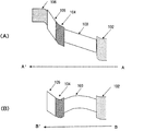
図1(A)〜図2(B)は、実施形態1の半導体装置10を説明する図である。半導体装置10は、npn形のヘテロ構造バイポーラトランジスタ(HBT)である。図1(A)と図1(B)は、それぞれ半導体装置10の断面と上面を模式的に示した図である。
101は半絶縁性のInP基板、
102はn形InPサブコレクタ層(n−InPサブコレクタ層と記載する。)、
103は低濃度のInGaAsコレクタ層、
104はn形InGaAsP電界制御層(n−InGaAsP電界制御層と記載する。)、
105は低濃度のInGaAsP中間層、
106は高濃度p形InGaAsベース層(p+−InGaAsベース層と記載する。)、
107はn形InPエミッタ層(n−InPエミッタ層と記載する。)、
108、109、110は、それぞれ、エミッタ電極、ベース電極、コレクタ電極
である。
(Embodiment 1)
1A to 2B are diagrams illustrating the
101 is a semi-insulating InP substrate,
103 is a low concentration InGaAs collector layer,
105 is a low concentration InGaAsP intermediate layer,
半導体装置10は、
InGaAsコレクタ層103が第1半導体層、
p+−InGaAsベース層106が第2半導体層、
n−InPサブコレクタ層102が第3半導体層、
InGaAsP中間層105が第4半導体層、
n−InPエミッタ層107が第6半導体層である。
The
An
a p + -
the n-
InGaAsP
The n-
ここで、InGaAsコレクタ層103とInGaAsP中間層105の低濃度とは、「空乏化したときに当該層内で大きな電界変化を引き起こすような電荷が殆んど生じない程度にドナー又はアクセプタの濃度が低い状態」を意味する。すなわち、InGaAsコレクタ層103とInGaAsP中間層105は、他のいずれのドーピング層と比較してもドナー又はアクセプタの濃度が低く、当該層をノンドープとしても半導体装置10は本発明の効果を得ることができる。また、p+−InGaAsベース層106の高濃度とは、「ベース電極109とオーミックコンタクトが可能な程度にアクセプタ濃度が高い」を意味する。例えば、p+−InGaAsベース層106は不純物濃度を1019/cm3以上とすることが好ましい。
Here, the low concentration of the
まず、半導体装置10の製造方法について説明する。半導体装置10を製作するには、まず、半絶縁性のInP基板101上に、102〜107の各半導体層をMO−VPE法によりエピタキシャル成長する。デバイスの製作は、まず、n−InPエミッタ層107のメサ、p+−InGaAsベース層106のメサ、低濃度のInGaAsP中間層105、n−InGaAsP電界制御層104、InGaAsコレクタ層103を含むコレクタメサ、n−InPサブコレクタ層102メサを、順次、4段のメサとして化学エッチング法により形成する。ここで、p+−InGaAsベース層106の加工の際に、その下層の低濃度のInGaAsP中間層105との界面でエッチングを停止しやすくするため、すなわち、低濃度のInGaAsP中間層105のエッチング速度をp+−InGaAsベース層106よりも相対的に小さくしておく。具体的には、低濃度のInGaAsP中間層105のバンドギャップエネルギーを1eV程度以上にする。
First, a method for manufacturing the
最後に、エミッタ電極108、ベース電極109、コレクタ電極110を形成する。これらの引き出し電極、層間の絶縁層、パッドなどは図示していないが、必要に応じてこれらも形成する。
Finally, an
図1(B)は上面図である。InP基板101側からn−InPサブコレクタ層102を含むサブコレクタメサ、InGaAsコレクタ層103からInGaAsP中間層105を含むコレクタメサ、p+−InGaAsベース層106を含むベースメサ、n−InPエミッタ層107を含むエミッタメサが形成されている。そして、上方にあるメサほど小さくなっており、コレクタメサの外周はサブコレクタメサの外周の内側にあり、ベースメサの外周はコレクタメサの外周の内側にあり、エミッタメサの外周はベースメサの内側にある。なお、各メサを矩形にしているが、その形状は矩形に限るものではない。
FIG. 1B is a top view. A subcollector mesa including an n-
半導体装置10のエミッタ電極108、ベース電極109、コレクタ電極110に適正なバイアス電圧(典型的にはエミッタに対して,ベースを+0.6〜0.8V程度,コレクタを+0.3〜3V程度)を印加して動作状態とした際の、ベース・コレクタ接合の活性部分(A−A’断面)及び周辺部分(B−B’断面)のバンドダイアグラムをそれぞれ図2(A)と図2(B)に示す。
Appropriate bias voltages for the
製造時に、図2(A)のようにp+−InGaAsベース層106の一部から、n−InPサブコレクタ層102の一部にわたり空乏化するようにn−InGaAsP電界制御層104のドーピング濃度を調整しておく。後述のようにn2−i−p部分の電位段差が適切な範囲(0.2V〜1.0V)となるように、例えば、n−InGaAsP電界制御層104の厚さは20〜40nmであり、そのドーピング濃度は2〜5×10¹⁷/cm3に調整される。
At the time of manufacturing, the doping concentration of the n-InGaAsP electric
半導体装置10の場合、導電形の配置は、基板側から、n1(n形)−i(真性)−n2(n形)−i(真性)−p(p形)の順となる。ここで、n2−i−p部分の電位段差が適切な範囲(0.2V〜1.0V)となることが重要であり、通常はおおむね0.5V〜0.8Vとすることが好ましい。この電位段差が大きすぎると、デバイス動作を維持できる最小のバイアス電圧(HBTの場合はベース・コレクタ電圧)が上昇してしまう。この段差は、HBTの動作にとって必要なものではないが、この電圧段差が応答特性を大きく変えるものではない。
In the case of the
一方、周辺部のB−B’断面においては、n−InPサブコレクタ層102から低濃度のInGaAsP中間層105まで、n1−i−n2−iの接続であり、p形の層は存在しない(図2(B))。ベース・コレクタ接合に逆バイアス電圧が印加された状態において、たとえn−InGaAsP電界制御層104の表面側の空乏化が多少生じても、その下部に電子が残留して中性層が残り、その下部への電界の進入をスクリーニングするため、低濃度のInGaAsコレクタ層103の電位降下は生じない。すなわち、コレクタメサのメサ側面(InGaAsコレクタ層103の側面)には電圧がかからないので、メサ側面が原因となる、順方向および逆方向のリーク電流の発生を低減させることができる。
On the other hand, in the BB ′ cross section of the peripheral portion, there is an n 1 -in 2 -i connection from the n-
実施形態1ではnpnトランジスタ構造を説明したが、導電型を反転させることでpnpトランジスタ構造とすることもできる。 Although the npn transistor structure has been described in the first embodiment, a pnp transistor structure can be obtained by inverting the conductivity type.
(実施形態2)
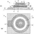
図3(A)〜図4(B)は、実施形態2の半導体装置20を説明する図である。半導体装置20はフォトダイオードである。図3(A)と図3(B)は、それぞれ半導体装置20の断面と上面を模式的に示した図である。
201は半絶縁性のInP基板、
202は高濃度のp形InGaAsP電極層(p+−InGaAsP電極層と記載する。)、
203はp形のInGaAs光吸収層(p−InGaAs光吸収層と記載する。)、
204は低濃度のInGaAs光吸収層(ud.−InGaAs光吸収層と記載する。)、
205はp形InGaAsP電界制御層(p−InGaAsP電界制御層と記載する。)、
206はノンドープInGaAsP中間層(ud.−InGaAsP中間層と記載する。)、
207はn形InGaAsP電界制御層(n−InGaAsP電界制御層と記載する。)、
208は低濃度のInGaAsP電子走行層(n−InGaAsP電子走行層と記載する。)、
209は高濃度のn形InGaAsP電極層(n+−InGaAsP電極層と記載する。)、
210は誘電体反射防止膜、
211はn電極、
212はp電極
である。
(Embodiment 2)
3A to 4B are diagrams illustrating the
201 is a semi-insulating InP substrate,
204 is a low-concentration InGaAs light absorption layer (referred to as ud.-InGaAs light absorption layer);
205 is a p-type InGaAsP electric field control layer (referred to as a p-InGaAsP electric field control layer),
206 is a non-doped InGaAsP intermediate layer (referred to as ud.-InGaAsP intermediate layer),
208 is a low concentration InGaAsP electron transit layer (referred to as an n-InGaAsP electron transit layer),
210 is a dielectric antireflection film,
211 is an n-electrode,
212 is a p-electrode.
半導体装置20は、
ud.−InGaAs光吸収層204が第1半導体層、
p−InGaAs光吸収層203が第2半導体層、
n−InGaAsP電子走行層207が第3半導体層、
ud.−InGaAsP中間層206が第5半導体層である。
The
ud. The InGaAs
The p-InGaAs
n-InGaAsP
ud. The -InGaAsP
ここで、「低濃度」及び「高濃度」とは、実施形態1での説明と同様の意味である。 Here, “low concentration” and “high concentration” have the same meaning as described in the first embodiment.
まず、半導体装置20の製造方法について説明する。半導体装置20を製作するには、まず、半絶縁性のInP基板201上に、202〜209までの各半導体層をMO−VPE法によりエピタキシャル成長する。その後、n+−InGaAsP電極層209、n−InGaAsP電子走行層208、n−InGaAsP電界制御層207からなる上部メサを化学エッチング法により形成する。ここでn−InGaAsP電界制御層207と、ud.−InGaAsP中間層206との組成を変えて、上層のエッチング速度を相対的に大きくして、エッチングが両層の界面付近で停止しやすくすることが好ましい。その後、ud.−InGaAsP中間層206からp−InGaAs光吸収層203までの中間部メサを形成、同様にしてp+−InGaAsP電極層202の下部メサを形成し、電気分離する。上部メサとその下部の中間部メサ内部がデバイスの活性部分(主領域)となる。その後、n電極211、p電極212を形成する。これらの引き出し電極、層間の絶縁層、パッドなどは図示していないが、必要に応じてこれらも形成する。最後に、誘電体反射防止膜210を形成する。
First, a method for manufacturing the
図3(B)は上面図である。InP基板201側からp+−InGaAsP電極層202を含む下部メサ、p−InGaAs光吸収層203からud.−InGaAsP中間層206を含む中間部メサ、n−InGaAsP電界制御層207からn+−InGaAsP電極層209を含む上部メサが形成されている。そして、上方にあるメサほど小さくなっており、中間部メサの外周は下部メサの外周の内側にあり、上部メサの外周は中間部メサの外周にある。なお、各メサを円形にしているが、その形状は円形に限るものではない。
FIG. 3B is a top view. The lower mesa including the p + -
半導体装置20の動作条件は、おおむね通常のpin形フォトダイオードと変わらない。n電極211とp電極212にバイアス電圧を印加したときの活性部分(A−A’断面)及び周辺部分(B−B’断面)のバンドダイアグラムをそれぞれ図4(A)と図4(B)に示す。図4(A)の活性部分は空乏化している。例えば、バイアス電圧は、1.5〜4Vの範囲である。
The operating conditions of the
製造時に、図4(A)のようにud.−InGaAs光吸収層204からn−InGaAsP電子走行層208に到る各層が空乏化するようにp−InGaAsP電界制御層205のドーピング濃度を調整しておく。後述のようにp−i−n部分の電位段差が適切な範囲(0.2V〜1.0V)となるように、p−InGaAsP電界制御層205の厚さは20〜40nmであり、そのドーピング濃度は2〜5×10¹⁷/cm3に調整される。
At the time of manufacture, as shown in FIG. The doping concentration of the p-InGaAsP electric
半導体装置20の場合、導電形の配置は、p−InGaAsP電界制御層205、ud.−InGaAsP中間層206、n−InGaAsP電界制御層207部分のp(p形)−i(真性)−n(n形)となる。このp−i−n部分の電位段差が適切な範囲(0.2V〜1.0V)となることが重要であり、通常はおおむね0.5V〜0.8Vとすることが好ましい。この電位段差が大きすぎると、デバイス動作を維持できる最小のバイアス電圧が上昇してしまう。この電位段差は、フォトダイオードの動作にとって必要なものではなく、従来のフォトダイオードには存在していなかった。半導体装置20は下記効果を得るためにこの電圧段差を設けるが、この電位段差はフォトダイオードの応答特性を大きく変えるものではない。
In the case of the
一方、中間部メサの周辺部(図3(A)のB−B’断面)は、p−InGaAs光吸収層203の側から、p1−i−p2−iの構造となっており、n形層は存在しない(図4(B))。接合に逆バイアス電圧が印加された状態において、たとえp−InGaAsP電界制御層205の表面側の空乏化が多少生じても、その下部にホールが残留して中性層が残るかぎり、その下部への電界の進入をスクリーニングするため、ud.−InGaAs光吸収層204の電位降下は生じない。すなわち、中間部メサのメサ側面(ud.−InGaAs光吸収層204の側面)には電圧がかからないので、メサ側面が原因となる逆方向のリーク電流の発生を低減させることができる。
On the other hand, the peripheral part of the intermediate mesa (BB ′ cross section in FIG. 3A) has a p 1 -i-p 2 -i structure from the p-InGaAs
半導体装置20のフォトダイオードは、p+−InGaAsP電極層202を下部メサに配置した反転形フォトダイオードである。従来、この種のフォトダイオード構造では、p+−InGaAsP電極層202に横方向の抵抗に起因するシリーズ抵抗が比較的高く、高速動作に影響を及ぼす傾向があった。しかし、半導体装置20は、中間部メサ側面のud.−InGaAs光吸収層204には電圧がかからないので、逆方向のリーク電流の増大を引き起こすことなく中間部メサの横方向サイズを縮小することが可能となり、その分シリーズ抵抗を低減することができる。また、中間部メサの縮小は、デバイス全体のサイズの縮小にも貢献し、2個以上のフォトダイオードの距離を近接させることが可能となり、半導体装置20は、アレイ状に高密度に配置可能である。
The photodiode of the
(実施形態3)
図5は、実施形態3の半導体装置30を説明する図である。半導体装置30は、電界吸収効果を使ったリッジ光導波路形の光変調器である。図5は半導体装置30の断面を模式的に示した図である。
301は半絶縁性基板のInP基板、
302はn電極層を兼ねた光クラッド(n−InP光クラッドと記載する。)、
303は光閉じ込め層(ud.−InGaAsP光閉じ込め層と記載する。)、
304は電界吸収効果を持つコア層(InGaAs/InGaAlAs多重量子井戸で構成されている。)、
305は光閉じ込め層(ud.−InGaAsP光閉じ込め層と記載する。)、
306はn形InGaAsP電界制御層(n−InGaAsP電界制御層と記載する。)、
307は接続層(ud.−InGaAsP接続層と記載する。)
308は光クラッド(p−InP光クラッドと記載する。)
309はp形InGaAsP電極層(p+−InGaAsP電極層と記載する。)
310はp電極
311はn電極
である。
(Embodiment 3)
FIG. 5 is a diagram illustrating the
301 is a semi-insulating InP substrate,
302 is an optical clad also serving as an n-electrode layer (referred to as an n-InP optical clad),
303 is an optical confinement layer (referred to as ud.-InGaAsP optical confinement layer),
304 is a core layer having an electroabsorption effect (consisting of InGaAs / InGaAlAs multiple quantum wells),
305 is an optical confinement layer (referred to as ud.-InGaAsP optical confinement layer),
308 is an optical cladding (referred to as a p-InP optical cladding).
310 is a p-
半導体装置30は、
コア層304及びud.−InGaAsP光閉じ込め層305が第1半導体層、
p−InP光クラッド308が第2半導体層、
ud.−InGaAsP光閉じ込め層303が第3半導体層、
ud.−InGaAsP接続層307が第4半導体層である。
The
p-InP
ud. The InGaAsP
ud. The
半導体装置30は、pnの極性は異なるものの、各層の積層配置は実施形態2の半導体装置20に類似している。導波路形の光変調器として機能すべく、半導体装置20のud.−InGaAs光吸収層204、p−InGaAsP電界制御層207が、半導体装置30では、それぞれ、コア層304、p−InP光クラッド308に置き換えされている。
Although the
基板側のn−InP光クラッド302からp−InP光クラッド308まで到る導電形は、実施形態1の半導体装置10と同じく、n1−i−n2−i−pである。すなわち、半導体装置10と同様の構造がリッジ光導波路形の光変調器のコア層と光閉じ込め層として組み込まれている。
It reaches conductivity type from n-InP
ud.−InGaAsP接続層307の上面は、p−InP光クラッド308が配置される部分とp−InP光クラッド308が無い露出部分がある。露出部分のud.−InGaAsP接続層307から下部のメサは、n1−i−n2−iの積層構造となる。したがって、デバイスに逆バイアスを印加した動作状態においても、n−InGaAsP電界制御層306に電子が残留する中性領域が形成され、メサ側面に露出するコア層304の側面は電圧降下が生じない、もしくは、低減される。その結果、メサ側面に起因するリーク電流の発生を抑制することができる。
ud. The upper surface of the -
(本発明の効果)
バンドギャップの小さなInGaAsなどをその内部に含むpn接合は、様々な電子デバイスや光デバイスに採用されている。しかし、高速動作を目的としてメサ形のデバイスとした場合、リーク電流が発生しやすいという課題解決のためデバイスのサイズを大きくせざるを得ないという制約があった。
(Effect of the present invention)
A pn junction including InGaAs having a small band gap therein is employed in various electronic devices and optical devices. However, when a mesa-type device is used for the purpose of high-speed operation, there is a restriction that the size of the device must be increased in order to solve the problem that leakage current is likely to occur.
本発明は、デバイス動作にとって、本来は不要な電位段差(第4半導体層又は第5半導体層)をデバイスの構造内にあえて挿入したものである。この電位段差は、バンドギャップの小さな半導体がメサ側面に露出しても、その部分の電位降下量を抑制し、デバイス動作に不都合なリーク電流を低減できる、という機能をもたらす。この効果は、ヘテロ構造バイポーラトランジスタ、フォトダイオード、及び電界吸収形光変調器などに共通して得られる。また、フォトダイオードにおいては、リーク電流が緩和されるのでデバイスのサイズを縮小することが可能となり、シリーズ抵抗の低減による動作速度の改善のみならず、デバイスを高密度にアレイ状に配置できるという利点も生まれる。 In the present invention, a potential step (a fourth semiconductor layer or a fifth semiconductor layer) that is originally unnecessary for device operation is inserted in the device structure. Even if a semiconductor having a small band gap is exposed on the side surface of the mesa, this potential step provides a function of suppressing the amount of potential drop at that portion and reducing a leakage current that is inconvenient for device operation. This effect is obtained in common with heterostructure bipolar transistors, photodiodes, electroabsorption optical modulators, and the like. In addition, since the leakage current is reduced in the photodiode, the size of the device can be reduced, and not only the operation speed is improved by reducing the series resistance, but also the advantage that the devices can be arranged in a high density array. Is also born.
(他の実施形態)
実施形態1〜3においては、各層の半導体材料としてInP、InGaAs、InGaAsPを用いた半導体デバイス構造について説明したが、各層の半導体材料は上記に限らず、他の半導体材料を用いたデバイスにも同様に応用できる。
(Other embodiments)
In the first to third embodiments, the semiconductor device structure using InP, InGaAs, or InGaAsP as the semiconductor material of each layer has been described. However, the semiconductor material of each layer is not limited to the above, and the same applies to devices using other semiconductor materials. It can be applied to.
10、20、30:半導体装置
50:HBT
60:フォトダイオード
101:InP基板、
102:n−InPサブコレクタ層
103:InGaAsコレクタ層
104:n−InGaAsP電界制御層
105:InGaAsP中間層
106:p+−InGaAsベース層
107:n−InPエミッタ層
108:エミッタ電極
109:ベース電極
110:コレクタ電極
201:InP基板
202:p+−InGaAsP電極層
203:p−InGaAs光吸収層
204:ud.−InGaAs光吸収層
205:p−InGaAsP電界制御層
206:ud.−InGaAsP中間層
207:n−InGaAsP電界制御層
208:n−InGaAsP電子走行層
209:n+−InGaAsP電極層
210:誘電体反射防止膜
211:n電極、
212:p電極
301:InP基板、
302:n−InP光クラッド
303:ud.−InGaAsP光閉じ込め層
304:コア層
305:ud.−InGaAsP光閉じ込め層
306:n−InGaAsP電界制御層
307:ud.−InGaAsP接続層
308:p−InP光クラッド
309:p+−InGaAsP電極層
310:p電極
311:n電極
501:半絶縁性InP基板
502:InPサブコレクタ層
503:n形InGaAsコレクタ層
506:p形InGaAsベース層
507:n形InPエミッタ層
508:エミッタ電極
509:ベース電極
510:コレクタ電極
601:半絶縁性InP
602:n形InPコンタクト層
603:InGaAs光吸収層
604:InGaAsP表面カバー層
605:p形InPコンタクト層
606:p電極
607:n電極
10, 20, 30: Semiconductor device 50: HBT
60: Photodiode 101: InP substrate,
102: n-InP subcollector layer 103: InGaAs collector layer
104: n-InGaAsP electric field control layer 105: InGaAsP intermediate layer 106: p + -InGaAs base layer 107: n-InP emitter layer 108: emitter electrode 109: base electrode 110: collector electrode 201: InP substrate 202: p + -InGaAsP Electrode layer 203: p-InGaAs light absorption layer 204: ud. -InGaAs light absorption layer 205: p-InGaAsP electric field control layer 206: ud. InGaAsP intermediate layer 207: n-InGaAsP electric field control layer 208: n-InGaAsP electron transit layer 209: n + -InGaAsP electrode layer 210: dielectric antireflection film 211: n electrode,
212: p-electrode 301: InP substrate,
302: n-InP optical cladding 303: ud. InGaAsP optical confinement layer 304: core layer 305: ud. InGaAsP optical confinement layer 306: n-InGaAsP electric field control layer 307: ud. -InGaAsP connection layer 308: p-InP optical cladding 309: p + -InGaAsP electrode layer 310: p electrode 311: n electrode 501: semi-insulating InP substrate 502: InP subcollector layer 503: n-type InGaAs collector layer 506: p InGaAs base layer 507: n-type InP emitter layer 508: emitter electrode 509: base electrode 510: collector electrode 601: semi-insulating InP
602: n-type InP contact layer 603: InGaAs light absorption layer 604: InGaAsP surface cover layer 605: p-type InP contact layer 606: p-electrode 607: n-electrode
Claims (8)
前記基板側から前記第3半導体層、前記第1半導体層、前記第4a半導体層、前記第4b半導体層、前記第2半導体層の順で積層しており、
前記第1半導体層及び前記第4b半導体層は、不純物濃度が前記第2半導体層及び前記第3半導体層より低濃度であり、
前記第4a半導体層及び前記第4b半導体層は、バンドギャップが前記第1半導体層及び前記第2半導体層より大きく、
前記第2半導体層の外周が前記第4b半導体層の外周より内側にあることを特徴とする半導体装置。 A first semiconductor layer, a p-type second semiconductor layer, an n-type third semiconductor layer, an n-type fourth a semiconductor layer, and a fourth b semiconductor layer are stacked in parallel with the substrate surface on one side of the substrate. A semiconductor device,
The third semiconductor layer, the first semiconductor layer, the 4a semiconductor layer, the 4b semiconductor layer, and the second semiconductor layer are stacked in this order from the substrate side.
The first semiconductor layer and the fourth b semiconductor layer have an impurity concentration lower than that of the second semiconductor layer and the third semiconductor layer,
The 4a semiconductor layer and the 4b semiconductor layer have a band gap larger than that of the first semiconductor layer and the second semiconductor layer,
A semiconductor device, wherein an outer periphery of the second semiconductor layer is inside an outer periphery of the fourth b semiconductor layer.
前記基板側から前記第2半導体層、前記第1半導体層、前記第5a半導体層、前記第5b半導体層、前記第3半導体層の順で積層しており、
前記第1半導体層及び前記第5b半導体層は、不純物濃度が前記第2半導体層及び前記第3半導体層より低濃度であり、
前記第5a半導体層及び前記第5b半導体層は、バンドギャップが前記第1半導体層及び前記第2半導体層より大きく、
前記第3半導体層の外周が前記第5b半導体層の外周より内側にあることを特徴とする半導体装置。 A first semiconductor layer, a p-type second semiconductor layer, an n-type third semiconductor layer, a p-type 5a semiconductor layer, and a 5b semiconductor layer are stacked in parallel with the substrate surface on one side of the substrate. A semiconductor device,
The second semiconductor layer, the first semiconductor layer, the 5a semiconductor layer, the 5b semiconductor layer, and the third semiconductor layer are stacked in this order from the substrate side,
The first semiconductor layer and the 5b semiconductor layer have a lower impurity concentration than the second semiconductor layer and the third semiconductor layer,
The 5a semiconductor layer and the 5b semiconductor layer have a band gap larger than that of the first semiconductor layer and the second semiconductor layer,
A semiconductor device, wherein an outer periphery of the third semiconductor layer is inside an outer periphery of the fifth b semiconductor layer.
前記基板側から前記第3半導体層、前記第1半導体層、前記第4a半導体層、前記第4b半導体層、前記第2半導体層の順で積層しており、
前記第1半導体層及び前記第4b半導体層は、不純物濃度が前記第2半導体層及び前記第3半導体層より低濃度であり、
前記第2半導体層の外周が前記第4b半導体層の外周より内側にあることを特徴とする半導体装置。 A first semiconductor layer, a p-type second semiconductor layer, an n-type third semiconductor layer, an n-type fourth a semiconductor layer, and a fourth b semiconductor layer are stacked in parallel with the substrate surface on one side of the substrate. A semiconductor device,
The third semiconductor layer, the first semiconductor layer, the 4a semiconductor layer, the 4b semiconductor layer, and the second semiconductor layer are stacked in this order from the substrate side.
The first semiconductor layer and the fourth b semiconductor layer have an impurity concentration lower than that of the second semiconductor layer and the third semiconductor layer,
A semiconductor device, wherein an outer periphery of the second semiconductor layer is inside an outer periphery of the fourth b semiconductor layer.
Priority Applications (5)
| Application Number | Priority Date | Filing Date | Title |
|---|---|---|---|
| JP2011012277A JP5649219B2 (en) | 2011-01-24 | 2011-01-24 | Semiconductor device |
| CN201280010887.1A CN103403848B (en) | 2011-01-24 | 2012-01-20 | Semiconductor device |
| EP12739690.1A EP2669934B1 (en) | 2011-01-24 | 2012-01-20 | Semiconductor device |
| US13/981,050 US8754445B2 (en) | 2011-01-24 | 2012-01-20 | Semiconductor device |
| PCT/JP2012/051178 WO2012102196A1 (en) | 2011-01-24 | 2012-01-20 | Semiconductor device |
Applications Claiming Priority (1)
| Application Number | Priority Date | Filing Date | Title |
|---|---|---|---|
| JP2011012277A JP5649219B2 (en) | 2011-01-24 | 2011-01-24 | Semiconductor device |
Publications (2)
| Publication Number | Publication Date |
|---|---|
| JP2012156206A JP2012156206A (en) | 2012-08-16 |
| JP5649219B2 true JP5649219B2 (en) | 2015-01-07 |
Family
ID=46580765
Family Applications (1)
| Application Number | Title | Priority Date | Filing Date |
|---|---|---|---|
| JP2011012277A Active JP5649219B2 (en) | 2011-01-24 | 2011-01-24 | Semiconductor device |
Country Status (5)
| Country | Link |
|---|---|
| US (1) | US8754445B2 (en) |
| EP (1) | EP2669934B1 (en) |
| JP (1) | JP5649219B2 (en) |
| CN (1) | CN103403848B (en) |
| WO (1) | WO2012102196A1 (en) |
Families Citing this family (7)
| Publication number | Priority date | Publication date | Assignee | Title |
|---|---|---|---|---|
| SG11201606994XA (en) * | 2014-02-26 | 2016-09-29 | Toray Industries | Polyimide resin, resin composition using same, and laminated film |
| FR3053836B1 (en) * | 2016-07-08 | 2019-07-05 | Thales | RADIATION DETECTOR AND ASSOCIATED OMAGER |
| US9726841B1 (en) * | 2016-07-12 | 2017-08-08 | Inphi Corporation | Integrated photo detector, method of making the same |
| CN109786246A (en) * | 2017-11-10 | 2019-05-21 | 中芯国际集成电路制造(上海)有限公司 | Fin bipolar junction transistor and forming method thereof |
| US10727948B2 (en) | 2018-04-05 | 2020-07-28 | Nokia Solutions And Networks Oy | Communication system employing surface-coupled optical devices |
| US10411807B1 (en) | 2018-04-05 | 2019-09-10 | Nokia Solutions And Networks Oy | Optical transmitter having an array of surface-coupled electro-absorption modulators |
| US10739622B2 (en) * | 2018-12-28 | 2020-08-11 | Juniper Networks, Inc. | Integrated optoelectronic device with heater |
Family Cites Families (15)
| Publication number | Priority date | Publication date | Assignee | Title |
|---|---|---|---|---|
| JPS60242671A (en) * | 1984-05-16 | 1985-12-02 | Nippon Telegr & Teleph Corp <Ntt> | Hetero-junction bipolar transistor |
| JPH05243252A (en) * | 1992-02-27 | 1993-09-21 | Nec Corp | Maufacture of bipolar transistor |
| JP3016302B2 (en) * | 1992-04-23 | 2000-03-06 | 日本電気株式会社 | Pnpn semiconductor device and its driving circuit |
| JPH07254612A (en) * | 1994-03-14 | 1995-10-03 | Furukawa Electric Co Ltd:The | Heterojunction bipolar transistor |
| US6677619B1 (en) * | 1997-01-09 | 2004-01-13 | Nichia Chemical Industries, Ltd. | Nitride semiconductor device |
| JP3246401B2 (en) * | 1997-07-15 | 2002-01-15 | 日本電気株式会社 | Heterojunction bipolar transistor |
| JP4093304B2 (en) * | 2002-06-26 | 2008-06-04 | Nttエレクトロニクス株式会社 | Avalanche photodiode |
| US6927412B2 (en) * | 2002-11-21 | 2005-08-09 | Ricoh Company, Ltd. | Semiconductor light emitter |
| US6998320B2 (en) * | 2003-04-23 | 2006-02-14 | Triquint Semiconductor, Inc. | Passivation layer for group III-V semiconductor devices |
| US7142342B2 (en) * | 2003-06-02 | 2006-11-28 | Avago Technologies Fiber Ip (Singapore) Pte. Ltd. | Electroabsorption modulator |
| JP4127815B2 (en) * | 2003-11-10 | 2008-07-30 | 日本電信電話株式会社 | Avalanche photodiode |
| US7115918B2 (en) * | 2004-02-11 | 2006-10-03 | Xindium Technologies, Inc. | Collector layer structure for a double hetero-junction bipolar transistor for power amplification applications |
| JP5025330B2 (en) * | 2007-05-22 | 2012-09-12 | 三菱電機株式会社 | Semiconductor light receiving element and manufacturing method thereof |
| JP2009021454A (en) * | 2007-07-13 | 2009-01-29 | Yokogawa Electric Corp | Semiconductor optical element |
| JP4728386B2 (en) | 2008-12-17 | 2011-07-20 | Nttエレクトロニクス株式会社 | Avalanche photodiode |
-
2011
- 2011-01-24 JP JP2011012277A patent/JP5649219B2/en active Active
-
2012
- 2012-01-20 EP EP12739690.1A patent/EP2669934B1/en active Active
- 2012-01-20 CN CN201280010887.1A patent/CN103403848B/en active Active
- 2012-01-20 US US13/981,050 patent/US8754445B2/en active Active
- 2012-01-20 WO PCT/JP2012/051178 patent/WO2012102196A1/en active Application Filing
Also Published As
| Publication number | Publication date |
|---|---|
| WO2012102196A1 (en) | 2012-08-02 |
| US20130313608A1 (en) | 2013-11-28 |
| CN103403848A (en) | 2013-11-20 |
| EP2669934B1 (en) | 2020-08-26 |
| CN103403848B (en) | 2016-02-24 |
| JP2012156206A (en) | 2012-08-16 |
| EP2669934A1 (en) | 2013-12-04 |
| US8754445B2 (en) | 2014-06-17 |
| EP2669934A4 (en) | 2018-01-24 |
Similar Documents
| Publication | Publication Date | Title |
|---|---|---|
| JP5649219B2 (en) | Semiconductor device | |
| US7829915B2 (en) | Avalanche photodiode | |
| US5557117A (en) | Heterojunction bipolar transistor and integrated circuit device using the same | |
| JP4728386B2 (en) | Avalanche photodiode | |
| US4682196A (en) | Multi-layered semi-conductor photodetector | |
| US20080121867A1 (en) | Avalanche Photodiode | |
| US20100189154A1 (en) | Semiconductor optical device | |
| JP5631668B2 (en) | Avalanche photodiode | |
| US7855400B2 (en) | Semiconductor light detecting element and method for manufacturing the semiconductor light detecting element | |
| JP5433948B2 (en) | Semiconductor photo detector | |
| JP5327892B2 (en) | Avalanche photodiode | |
| US20100133637A1 (en) | Avalanche photodiode | |
| US5880489A (en) | Semiconductor photodetector | |
| JP5746222B2 (en) | Opto-electronic devices | |
| US6692837B2 (en) | Semi-insulating substrate, semiconductor optical device and fabrication method of semiconductor thin film | |
| JPH0513882A (en) | Semiconductor optical element using wide band gap material for p-n current blocking layer | |
| JP5303793B2 (en) | Photodiode | |
| JP2014110380A (en) | Array-type light receiving element and method for manufacturing array-type light receiving element | |
| US9911889B2 (en) | Method for fabricating a heterojunction schottky gate bipolar transistor | |
| JP2014060190A (en) | Semiconductor device and semiconductor device manufacturing method | |
| JPH11133367A (en) | Semiconductor optical modulation device and its production | |
| WO2023201209A1 (en) | Suppression of phototransistor gain in an optical modulator | |
| US20180254300A1 (en) | Photodiode matrix with isolated cathodes | |
| JPWO2010035508A1 (en) | Semiconductor light receiving element and manufacturing method thereof | |
| JP2016004936A (en) | Light-receiving element and epitaxial wafer |
Legal Events
| Date | Code | Title | Description |
|---|---|---|---|
| A621 | Written request for application examination |
Free format text: JAPANESE INTERMEDIATE CODE: A621 Effective date: 20130215 |
|
| A131 | Notification of reasons for refusal |
Free format text: JAPANESE INTERMEDIATE CODE: A131 Effective date: 20140408 |
|
| A521 | Request for written amendment filed |
Free format text: JAPANESE INTERMEDIATE CODE: A523 Effective date: 20140530 |
|
| A131 | Notification of reasons for refusal |
Free format text: JAPANESE INTERMEDIATE CODE: A131 Effective date: 20140617 |
|
| A521 | Request for written amendment filed |
Free format text: JAPANESE INTERMEDIATE CODE: A523 Effective date: 20140808 |
|
| A131 | Notification of reasons for refusal |
Free format text: JAPANESE INTERMEDIATE CODE: A131 Effective date: 20140826 |
|
| A521 | Request for written amendment filed |
Free format text: JAPANESE INTERMEDIATE CODE: A523 Effective date: 20141008 |
|
| TRDD | Decision of grant or rejection written | ||
| A01 | Written decision to grant a patent or to grant a registration (utility model) |
Free format text: JAPANESE INTERMEDIATE CODE: A01 Effective date: 20141105 |
|
| A61 | First payment of annual fees (during grant procedure) |
Free format text: JAPANESE INTERMEDIATE CODE: A61 Effective date: 20141110 |
|
| R150 | Certificate of patent or registration of utility model |
Ref document number: 5649219 Country of ref document: JP Free format text: JAPANESE INTERMEDIATE CODE: R150 |
|
| R250 | Receipt of annual fees |
Free format text: JAPANESE INTERMEDIATE CODE: R250 |
|
| R250 | Receipt of annual fees |
Free format text: JAPANESE INTERMEDIATE CODE: R250 |
|
| R250 | Receipt of annual fees |
Free format text: JAPANESE INTERMEDIATE CODE: R250 |
|
| R250 | Receipt of annual fees |
Free format text: JAPANESE INTERMEDIATE CODE: R250 |
|
| R250 | Receipt of annual fees |
Free format text: JAPANESE INTERMEDIATE CODE: R250 |
|
| R250 | Receipt of annual fees |
Free format text: JAPANESE INTERMEDIATE CODE: R250 |
|
| S533 | Written request for registration of change of name |
Free format text: JAPANESE INTERMEDIATE CODE: R313533 |
|
| R350 | Written notification of registration of transfer |
Free format text: JAPANESE INTERMEDIATE CODE: R350 |
|
| R250 | Receipt of annual fees |
Free format text: JAPANESE INTERMEDIATE CODE: R250 |