EP3557565A1 - Anzeigetafel und verfahren zur herstellung eines anzeigesubstrat - Google Patents
Anzeigetafel und verfahren zur herstellung eines anzeigesubstrat Download PDFInfo
- Publication number
- EP3557565A1 EP3557565A1 EP19166452.3A EP19166452A EP3557565A1 EP 3557565 A1 EP3557565 A1 EP 3557565A1 EP 19166452 A EP19166452 A EP 19166452A EP 3557565 A1 EP3557565 A1 EP 3557565A1
- Authority
- EP
- European Patent Office
- Prior art keywords
- light emitting
- substrate
- driving
- emitting element
- display device
- Prior art date
- Legal status (The legal status is an assumption and is not a legal conclusion. Google has not performed a legal analysis and makes no representation as to the accuracy of the status listed.)
- Granted
Links
Images




Classifications
-
- G—PHYSICS
- G09—EDUCATION; CRYPTOGRAPHY; DISPLAY; ADVERTISING; SEALS
- G09G—ARRANGEMENTS OR CIRCUITS FOR CONTROL OF INDICATING DEVICES USING STATIC MEANS TO PRESENT VARIABLE INFORMATION
- G09G3/00—Control arrangements or circuits, of interest only in connection with visual indicators other than cathode-ray tubes
- G09G3/20—Control arrangements or circuits, of interest only in connection with visual indicators other than cathode-ray tubes for presentation of an assembly of a number of characters, e.g. a page, by composing the assembly by combination of individual elements arranged in a matrix no fixed position being assigned to or needed to be assigned to the individual characters or partial characters
-
- G—PHYSICS
- G09—EDUCATION; CRYPTOGRAPHY; DISPLAY; ADVERTISING; SEALS
- G09G—ARRANGEMENTS OR CIRCUITS FOR CONTROL OF INDICATING DEVICES USING STATIC MEANS TO PRESENT VARIABLE INFORMATION
- G09G3/00—Control arrangements or circuits, of interest only in connection with visual indicators other than cathode-ray tubes
- G09G3/20—Control arrangements or circuits, of interest only in connection with visual indicators other than cathode-ray tubes for presentation of an assembly of a number of characters, e.g. a page, by composing the assembly by combination of individual elements arranged in a matrix no fixed position being assigned to or needed to be assigned to the individual characters or partial characters
- G09G3/2085—Special arrangements for addressing the individual elements of the matrix, other than by driving respective rows and columns in combination
- G09G3/2088—Special arrangements for addressing the individual elements of the matrix, other than by driving respective rows and columns in combination with use of a plurality of processors, each processor controlling a number of individual elements of the matrix
-
- G—PHYSICS
- G09—EDUCATION; CRYPTOGRAPHY; DISPLAY; ADVERTISING; SEALS
- G09G—ARRANGEMENTS OR CIRCUITS FOR CONTROL OF INDICATING DEVICES USING STATIC MEANS TO PRESENT VARIABLE INFORMATION
- G09G3/00—Control arrangements or circuits, of interest only in connection with visual indicators other than cathode-ray tubes
- G09G3/20—Control arrangements or circuits, of interest only in connection with visual indicators other than cathode-ray tubes for presentation of an assembly of a number of characters, e.g. a page, by composing the assembly by combination of individual elements arranged in a matrix no fixed position being assigned to or needed to be assigned to the individual characters or partial characters
- G09G3/22—Control arrangements or circuits, of interest only in connection with visual indicators other than cathode-ray tubes for presentation of an assembly of a number of characters, e.g. a page, by composing the assembly by combination of individual elements arranged in a matrix no fixed position being assigned to or needed to be assigned to the individual characters or partial characters using controlled light sources
- G09G3/30—Control arrangements or circuits, of interest only in connection with visual indicators other than cathode-ray tubes for presentation of an assembly of a number of characters, e.g. a page, by composing the assembly by combination of individual elements arranged in a matrix no fixed position being assigned to or needed to be assigned to the individual characters or partial characters using controlled light sources using electroluminescent panels
- G09G3/32—Control arrangements or circuits, of interest only in connection with visual indicators other than cathode-ray tubes for presentation of an assembly of a number of characters, e.g. a page, by composing the assembly by combination of individual elements arranged in a matrix no fixed position being assigned to or needed to be assigned to the individual characters or partial characters using controlled light sources using electroluminescent panels semiconductive, e.g. using light-emitting diodes [LED]
- G09G3/3208—Control arrangements or circuits, of interest only in connection with visual indicators other than cathode-ray tubes for presentation of an assembly of a number of characters, e.g. a page, by composing the assembly by combination of individual elements arranged in a matrix no fixed position being assigned to or needed to be assigned to the individual characters or partial characters using controlled light sources using electroluminescent panels semiconductive, e.g. using light-emitting diodes [LED] organic, e.g. using organic light-emitting diodes [OLED]
- G09G3/3225—Control arrangements or circuits, of interest only in connection with visual indicators other than cathode-ray tubes for presentation of an assembly of a number of characters, e.g. a page, by composing the assembly by combination of individual elements arranged in a matrix no fixed position being assigned to or needed to be assigned to the individual characters or partial characters using controlled light sources using electroluminescent panels semiconductive, e.g. using light-emitting diodes [LED] organic, e.g. using organic light-emitting diodes [OLED] using an active matrix
- G09G3/3233—Control arrangements or circuits, of interest only in connection with visual indicators other than cathode-ray tubes for presentation of an assembly of a number of characters, e.g. a page, by composing the assembly by combination of individual elements arranged in a matrix no fixed position being assigned to or needed to be assigned to the individual characters or partial characters using controlled light sources using electroluminescent panels semiconductive, e.g. using light-emitting diodes [LED] organic, e.g. using organic light-emitting diodes [OLED] using an active matrix with pixel circuitry controlling the current through the light-emitting element
-
- G—PHYSICS
- G09—EDUCATION; CRYPTOGRAPHY; DISPLAY; ADVERTISING; SEALS
- G09G—ARRANGEMENTS OR CIRCUITS FOR CONTROL OF INDICATING DEVICES USING STATIC MEANS TO PRESENT VARIABLE INFORMATION
- G09G3/00—Control arrangements or circuits, of interest only in connection with visual indicators other than cathode-ray tubes
- G09G3/20—Control arrangements or circuits, of interest only in connection with visual indicators other than cathode-ray tubes for presentation of an assembly of a number of characters, e.g. a page, by composing the assembly by combination of individual elements arranged in a matrix no fixed position being assigned to or needed to be assigned to the individual characters or partial characters
- G09G3/34—Control arrangements or circuits, of interest only in connection with visual indicators other than cathode-ray tubes for presentation of an assembly of a number of characters, e.g. a page, by composing the assembly by combination of individual elements arranged in a matrix no fixed position being assigned to or needed to be assigned to the individual characters or partial characters by control of light from an independent source
- G09G3/3406—Control of illumination source
- G09G3/342—Control of illumination source using several illumination sources separately controlled corresponding to different display panel areas, e.g. along one dimension such as lines
- G09G3/3426—Control of illumination source using several illumination sources separately controlled corresponding to different display panel areas, e.g. along one dimension such as lines the different display panel areas being distributed in two dimensions, e.g. matrix
-
- G—PHYSICS
- G09—EDUCATION; CRYPTOGRAPHY; DISPLAY; ADVERTISING; SEALS
- G09G—ARRANGEMENTS OR CIRCUITS FOR CONTROL OF INDICATING DEVICES USING STATIC MEANS TO PRESENT VARIABLE INFORMATION
- G09G3/00—Control arrangements or circuits, of interest only in connection with visual indicators other than cathode-ray tubes
- G09G3/20—Control arrangements or circuits, of interest only in connection with visual indicators other than cathode-ray tubes for presentation of an assembly of a number of characters, e.g. a page, by composing the assembly by combination of individual elements arranged in a matrix no fixed position being assigned to or needed to be assigned to the individual characters or partial characters
- G09G3/34—Control arrangements or circuits, of interest only in connection with visual indicators other than cathode-ray tubes for presentation of an assembly of a number of characters, e.g. a page, by composing the assembly by combination of individual elements arranged in a matrix no fixed position being assigned to or needed to be assigned to the individual characters or partial characters by control of light from an independent source
- G09G3/36—Control arrangements or circuits, of interest only in connection with visual indicators other than cathode-ray tubes for presentation of an assembly of a number of characters, e.g. a page, by composing the assembly by combination of individual elements arranged in a matrix no fixed position being assigned to or needed to be assigned to the individual characters or partial characters by control of light from an independent source using liquid crystals
-
- H—ELECTRICITY
- H10—SEMICONDUCTOR DEVICES; ELECTRIC SOLID-STATE DEVICES NOT OTHERWISE PROVIDED FOR
- H10K—ORGANIC ELECTRIC SOLID-STATE DEVICES
- H10K59/00—Integrated devices, or assemblies of multiple devices, comprising at least one organic light-emitting element covered by group H10K50/00
- H10K59/10—OLED displays
- H10K59/12—Active-matrix OLED [AMOLED] displays
- H10K59/131—Interconnections, e.g. wiring lines or terminals
-
- G—PHYSICS
- G09—EDUCATION; CRYPTOGRAPHY; DISPLAY; ADVERTISING; SEALS
- G09G—ARRANGEMENTS OR CIRCUITS FOR CONTROL OF INDICATING DEVICES USING STATIC MEANS TO PRESENT VARIABLE INFORMATION
- G09G2300/00—Aspects of the constitution of display devices
- G09G2300/04—Structural and physical details of display devices
- G09G2300/0404—Matrix technologies
- G09G2300/0413—Details of dummy pixels or dummy lines in flat panels
-
- G—PHYSICS
- G09—EDUCATION; CRYPTOGRAPHY; DISPLAY; ADVERTISING; SEALS
- G09G—ARRANGEMENTS OR CIRCUITS FOR CONTROL OF INDICATING DEVICES USING STATIC MEANS TO PRESENT VARIABLE INFORMATION
- G09G2300/00—Aspects of the constitution of display devices
- G09G2300/04—Structural and physical details of display devices
- G09G2300/0421—Structural details of the set of electrodes
- G09G2300/0426—Layout of electrodes and connections
-
- G—PHYSICS
- G09—EDUCATION; CRYPTOGRAPHY; DISPLAY; ADVERTISING; SEALS
- G09G—ARRANGEMENTS OR CIRCUITS FOR CONTROL OF INDICATING DEVICES USING STATIC MEANS TO PRESENT VARIABLE INFORMATION
- G09G2300/00—Aspects of the constitution of display devices
- G09G2300/08—Active matrix structure, i.e. with use of active elements, inclusive of non-linear two terminal elements, in the pixels together with light emitting or modulating elements
- G09G2300/0809—Several active elements per pixel in active matrix panels
- G09G2300/0819—Several active elements per pixel in active matrix panels used for counteracting undesired variations, e.g. feedback or autozeroing
-
- G—PHYSICS
- G09—EDUCATION; CRYPTOGRAPHY; DISPLAY; ADVERTISING; SEALS
- G09G—ARRANGEMENTS OR CIRCUITS FOR CONTROL OF INDICATING DEVICES USING STATIC MEANS TO PRESENT VARIABLE INFORMATION
- G09G2310/00—Command of the display device
- G09G2310/02—Addressing, scanning or driving the display screen or processing steps related thereto
- G09G2310/0264—Details of driving circuits
-
- G—PHYSICS
- G09—EDUCATION; CRYPTOGRAPHY; DISPLAY; ADVERTISING; SEALS
- G09G—ARRANGEMENTS OR CIRCUITS FOR CONTROL OF INDICATING DEVICES USING STATIC MEANS TO PRESENT VARIABLE INFORMATION
- G09G2320/00—Control of display operating conditions
- G09G2320/02—Improving the quality of display appearance
- G09G2320/0233—Improving the luminance or brightness uniformity across the screen
-
- G—PHYSICS
- G09—EDUCATION; CRYPTOGRAPHY; DISPLAY; ADVERTISING; SEALS
- G09G—ARRANGEMENTS OR CIRCUITS FOR CONTROL OF INDICATING DEVICES USING STATIC MEANS TO PRESENT VARIABLE INFORMATION
- G09G2330/00—Aspects of power supply; Aspects of display protection and defect management
- G09G2330/08—Fault-tolerant or redundant circuits, or circuits in which repair of defects is prepared
-
- G—PHYSICS
- G09—EDUCATION; CRYPTOGRAPHY; DISPLAY; ADVERTISING; SEALS
- G09G—ARRANGEMENTS OR CIRCUITS FOR CONTROL OF INDICATING DEVICES USING STATIC MEANS TO PRESENT VARIABLE INFORMATION
- G09G2330/00—Aspects of power supply; Aspects of display protection and defect management
- G09G2330/10—Dealing with defective pixels
-
- H—ELECTRICITY
- H10—SEMICONDUCTOR DEVICES; ELECTRIC SOLID-STATE DEVICES NOT OTHERWISE PROVIDED FOR
- H10K—ORGANIC ELECTRIC SOLID-STATE DEVICES
- H10K59/00—Integrated devices, or assemblies of multiple devices, comprising at least one organic light-emitting element covered by group H10K50/00
- H10K59/10—OLED displays
- H10K59/12—Active-matrix OLED [AMOLED] displays
-
- H—ELECTRICITY
- H10—SEMICONDUCTOR DEVICES; ELECTRIC SOLID-STATE DEVICES NOT OTHERWISE PROVIDED FOR
- H10K—ORGANIC ELECTRIC SOLID-STATE DEVICES
- H10K59/00—Integrated devices, or assemblies of multiple devices, comprising at least one organic light-emitting element covered by group H10K50/00
- H10K59/80—Constructional details
- H10K59/86—Series electrical configurations of multiple OLEDs
Definitions
- the present disclosure relates to a display device and a related manufacturing method of a display substrate, and more particularly, to a display device structure and a related manufacturing method of a display substrate that can increase the yield of the display device.
- Flat display and curved display device have gradually become the main products in the display device market due to characteristics of light weight and thin thickness, such as for applying to household televisions, personal computer monitors, and portable electronic devices such as phones, digital cameras and tablet computers.
- the design of the light source of flat display device and curved panel display device may include disposing conductive wires, electronic elements and light emitting elements on a substrate, and the electronic elements and conductive wires are used for transmitting signals to control the brightness or darkness of the display device.
- the inspection of the electronic elements is performed after the above elements are manufactured, and the corresponding light emitting elements will not emit light normally if any defect of the conductive wire or the electronic device occurs, which results in that the whole substrate has to be discarded.
- the present disclosure aims at providing a display device and related manufacturing method which may increase the stability of the transistor and/or may additionally improve the light uniformity of the display substrate.
- the display device includes a substrate and a light emitting unit, wherein the light emitting unit includes at least one light emitting element and at least two driving arrays.
- the at least one light emitting element is disposed on the substrate, and the at least one light emitting element has a first terminal and a second terminal.
- the at least two driving arrays are disposed on the substrate, wherein one of the at least two driving arrays is electrically connected to the first terminal of the at least one light emitting element.
- a manufacturing method of a display substrate includes providing a substrate, disposing at least two driving arrays on the substrate, inspecting at least one of the at least two driving arrays to confirm that at least one of the at least two driving arrays is qualified, disposing at least one light emitting element on the substrate, disposing at least one conductive element on the substrate, and electrically connecting the at least one light emitting element to one of the at least two driving arrays that is qualified.
- a manufacturing method of a display substrate is further provided by the present disclosure.
- the manufacturing method includes providing a substrate, disposing at least two driving arrays on the substrate, disposing at least one light emitting element on the substrate, electrically connecting the at least one light emitting element to one of the at least two driving arrays, and inspecting the at least one of the at least two driving arrays.
- the method further includes when an inspection result confirmed that the one of the at least two driving array is unqualified, removing the electrical connection between the unqualified driving array and the light emitting element and electrically connecting the light emitting element to another one of the at least two driving arrays.
- the corresponding features, areas, regions, steps, operations and/or components would be pointed to existence, but not limiting the existence or addition of one or more corresponding or other features, areas, regions, steps, operations and/or components.
- the corresponding component such as layer or area is referred to "on another component (or the variant thereof)” or “extend to another component”
- the component is referred to “directly on another component (or the variant thereof)” or “directly extend to another component”
- any component does not exist between them.
- the component is referred to “be coupled to another component (or the variant thereof)"
- it may be directly connected to another component, or may be indirectly connected (such as electrically connected) to another component through other component or components.
- liquid crystal display LCD
- electroluminescent display ELD
- organic light emitting diode display OLED display
- inorganic light emitting diode display LED display
- quantum dot display QD display
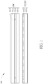
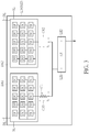
- FIG. 1 to FIG. 4 are schematic diagrams of structure and arrangement of elements of a display device according to a first embodiment of the present disclosure, wherein FIG. 1 is a cross-sectional schematic diagram of a structure of the display device according to the first embodiment of the present disclosure, FIG. 2 is a top-view schematic diagram of the substrate of the display device shown in FIG. 1 , FIG. 3 is an element arrangement schematic diagram of a single light emitting unit shown in FIG. 2 , and FIG. 4 is a partial equivalent circuit schematic diagram of a single driving array shown in FIG. 3 .
- the present disclosure provides a display device 100.
- the display device 100 may for example be a display such as (but not limited to) a liquid crystal display (LCD) that includes a backlight source 102 and a display panel 104.
- the display panel 104 for example may include a first substrate 1041, a second substrate 1042 and a display media layer 1043 between the first substrate 1041 and the second substrate 1042, and a sealant layer 1044 may be disposed between the first substrate 1041 and the second substrate 1042 to fix the first substrate 1041 and the second substrate 1042.
- the display media layer 1043 may be a liquid crystal layer
- the first substrate 1041 and the second substrate 1042 may be a transparent substrate respectively.
- the first substrate 1041 and the second substrate 1042 may independently be a hard substrate such as a glass substrate, a quartz substrate, and a sapphire substrate or a flexible substrate such as a plastic substrate that includes polyimide (PI), polycarbonate (PC) or polyethylene terephthalate (PET), but not limited thereto.
- PI polyimide
- PC polycarbonate
- PET polyethylene terephthalate
- some of the elements on the surfaces of the first substrate 1041 and the second substrate 1042 of FIG. 1 are omitted, such as circuit arrays, conductive lines, color filters, light shielding layer, but not limited thereto.
- the backlight source 102 of the present disclosure includes at least one light emitting unit LU disposed on the surface of a substrate 1021.
- the backlight source 102 of this embodiment may be an active-type backlight source that includes a plurality of light emitting units LU arranged in an array on the substrate 1021.
- the light emitting units LU arranged in an array and the related circuits are illustrated as a light emitting array layer 1022 in FIG. 1 .
- the display panel 104 is disposed at a side of the substrate 1021, wherein the display panel 104 in this embodiment is disposed at the side of the substrate 1021 that has light emitting units LU or light emitting array layer 1022 disposed thereon, but not limited thereto.
- the material of the substrate 1021 of the present disclosure may be equal to or not equal to the first substrate 1041 and the second substrate 1042, and the material of the substrate 1021 may refer to the material of the first substrate 1041 and the second substrate 1042 described above and not be described redundantly.
- the light emitting array layer 1022 includes at least one light emitting element LE and at least two driving arrays disposed on the substrate 1021, wherein the symbols DA1 and DA2 respectively represent one of the two driving arrays.
- one light emitting unit LU in this embodiment has two driving arrays DA1, DA2 and one light emitting element LE. That is, at least two driving arrays DA1, DA2 and at least one light emitting element LE compose a light emitting unit LU.
- the light emitting element LE has a first terminal LE1 and a second terminal LE2, wherein the first terminal LE1 and the second terminal LE2 for example may respectively be the anode and cathode of the light emitting element LE, but not limited thereto.
- the light emitting element LE may be any light emitting element, such as (but not limited to) a normal size light emitting diode (normal LED), a mini size light emitting diode (mini LED), a micro size light emitting diode (micro LED), an organic light emitting diode (OLED) or a quantum light emitting diode (QLED).
- Each of the driving arrays DA1, DA2 includes at least one driving unit DU.
- each of the driving arrays DA1, DA2 is electrically connected to the first terminal LE1 of the light emitting element LE, and the other one of the driving arrays DA1, DA2 is electrically isolated from the light emitting element LE.
- each of the driving arrays DA1, DA2 includes a plurality of driving units DU, and the driving units DU are electrically connected to each other in parallel and arranged in their corresponding driving array DA1 or DA2.
- the driving units DU connected in parallel may increase the total output current of one single driving array DA1 or DA2, so as to increase the brightness of the light emitting element LE.
- one driving array DA1 or DA2 may include 1 to 108 driving units DU arranged in an array, or may include 1 to 168 driving units DU arranged in an array, but not limited thereto.
- the light emitting unit LU of the display device 100 further includes a conductive element CE disposed between one of the at least two driving arrays DA1, DA2 and the light emitting element LE, and the conductive element CE is electrically connected between one of the driving arrays DA1, DA2 and the light emitting element LE.
- the conductive element CE of the present disclosure may include a zero-ohm resistor (a resistor with zero resistance), a conductive line or a Zener diode.
- the conductive element CE in this embodiment is a zero-ohm resistor, but not limited thereto.
- any appropriate conductive element with a low resistance, a resistance approaching to zero, or nearly without causing voltage drop may be applied to the conductive element CE of the present disclosure.
- the resistance of the conductive element CE may be in the range between 10 million ohms and 0 ohm, in the range between 50 ohms and 0 ohm, or in the range between 5 ohms and 0 ohm.
- the driving array DA1 includes at least one data line DL and at least one scan line SL, and the data line DL and the scan line SL are electrically connected to one or more corresponding driving units DU in the driving array DA1.
- Each of the driving units DU includes a first transistor TFT1, a second transistor TFT2 and a capacitor CST.
- the first transistor TFT1 may serve as a switch element of the driving unit DU and may include a gate electrode GE1, a source electrode SE1, and a drain electrode DE1.
- the gate electrode GE1 is electrically connected to the corresponding scan line SL
- the source electrode SE1 is electrically connected to the corresponding data line DL.
- the second transistor TFT2 may serve as a driving element of the driving unit DU and may include a gate electrode GE2, a source electrode SE2, and a drain electrode DE2.
- the gate electrode GE2 is electrically connected to the drain electrode DE1 of the first transistor TFT1
- the source electrode SE2 is electrically connected to an output terminal OE of the driving unit DU
- the drain electrode DE2 is electrically connected to a working voltage source Vdd.
- a first electrode of a capacitor CST is electrically connected to the drain electrode DE1 of the first transistor TFT1 and the gate electrode GE2 of the second transistor TFT2, and a second electrode of the capacitor CST is electrically connected to the output terminal OE of the driving unit DU and the source electrode SE2 of the second transistor TFT2.
- the driving unit DU is not limited to the design of having two transistors and one capacitor (2T1C).
- the driving unit DU may include various numbers of transistors and capacitors.
- the driving unit DU may include (but not limited to) seven transistors and one capacitor (7T1C).
- the second transistor TFT2 of the driving unit DU may be a transistor having four terminal-electrodes, and therefore the second transistor TFT2 further includes a fourth electrode FE which is electrically connected to the second electrode of the capacitor CST, the source electrode SE2 of the second transistor TFT2 and the output terminal OE of the driving unit DU at the same time.
- the present disclosure may reduce the variation of the threshold voltage Vt through electrically connecting the fourth electrode FE and the source electrode SE2 of the second transistor TFT2.
- the design of the present disclosure makes the fourth electrode FE of the second transistor TFT2 be electrically connected to the source electrode SE2 of the second transistor TFT2 and the output terminal OE of the driving unit DU, that is, be electrically connected to the light emitting element LE, so as to provide a compensation effect to the light emitting element LE through the voltage VG' of the fourth electrode FE and mitigate the mura phenomenon of non-uniform brightness resulted from the variations of the voltage Vf of each light emitting element LE in prior art.
- the present disclosure is not limited to the above description.
- the second transistor TFT2 may not include the fourth electrode FE.
- one of the advantages of disposing at least two driving arrays DA1 and DA2 in the light emitting unit LU is that when one of the driving arrays DA1 and DA2 has defects, another one of the driving arrays DA1 and DA2 may serve as a spare driving array, so as to increase the fabrication yield of the light emitting unit LU.
- Such design may avoid discarding the whole substrate 1021 with all the light emitting units LU due to any defect of the driving array DA1 or the driving array DA2, and thus the manufacturing cost can be lowered.
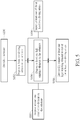
- the present disclosure also provides a manufacturing method of the display substrate 200, such as (but not limited to) the manufacturing method of disposing the conductive element CE after disposing the light emitting element LE or disposing the conductive element CE before the light emitting element LE, as shown in FIG. 5 .
- the above-mentioned display substrate 200 means a substrate that can provide light source, and the display substrate 200 may even be a substrate that can provide light with different brightness or different color in different regions.
- the display substrate 200 in this embodiment can serves as the backlight source 102 in FIG. 1 .
- the manufacturing method of the substrate 200 includes:
- every light emitting unit LU includes at least one light emitting element LE and at least two driving arrays DA1, DA2 (that is, at least one light emitting element LE and at least two driving arrays DA1, DA2 compose one light emitting unit LU), and a predetermined position CR1 and a predetermined position CR2 for disposing the conductive element CE may be reserved between the light emitting element LE and the driving arrays DA1, DA2.
- the light emitting unit LU can be defined as the following: when the conductive element CE is disposed on the predetermined position CR1 or CR2, the conductive element CE will not cross over (will not be electrically connected to) other conductive lines that are in the same layer as the conductive element CE. Accordingly, the light emitting element LE and the driving arrays DA1 and DA2 that have the above-mentioned characteristic of without crossing over other conductive lines will be considered as belonging to the same light emitting unit LU.
- the driving array DA1 passes the inspection and is qualified (Step S104)
- the conductive element CE will be disposed at the predetermined position CR1.
- the driving array DA1 is electrically connected to the light emitting element LE.
- the driving array DA2 is electrically isolated from the light emitting element LE and the driving array DA2 may be considered as a redundant array.
- a further inspection to the driving array DA2 may be performed. If the driving array DA2 is confirmed to pass the inspection and be a qualified driving array, the conductive element CE may be disposed at the predetermined position CR2 to electrically connect the driving array DA2 to the light emitting element LE.
- the driving array DA1 may be considered as a redundant array because it is electrically isolated from the light emitting element LE, and meanwhile the driving array DA2 can be considered as the driving array of the light emitting element LE since it is electrically connected to the light emitting element LE.
- the procedure of disposing the conductive element CE may be performed before or after Step S106.
- the procedure of Step S104 of inspecting the quality of the driving arrays DA1, DA2 may be performed before or after Step S106 of disposing the light emitting element LE on the substrate 1021.
- the method of inspecting the driving arrays DA1, DA2 may for example include inspecting the current and/or the voltage of the driving arrays DA1, DA2 through a probe and pin(s) or connection pad(s) on the substrate 1021, so as to discover whether the driving arrays DA1, DA2 are qualified or have defects.
- FIG. 5 illustrates that the conductive element CE is disposed after or before disposing the light emitting element LE on the substrate 1021, for instance.
- the display device and the manufacturing method of the display substrate of the present disclosure are not limited to the above embodiments.
- the following description will detail other embodiments or variant embodiments of the present disclosure.
- the same components are denoted by the same symbols in the following, and the repeated part will not be redundantly described.
- each element or material in the following embodiments of the present disclosure may refer to the above embodiments, therefore will not be redundantly described.
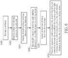
- FIG. 6 is a schematic diagram of process flow of a manufacturing method of a display substrate according to another embodiment of the present disclosure.
- the manufacturing method of the display substrate of this embodiment includes the following steps:
- one of the two driving arrays DA1, DA2 is electrically connected to the light emitting element LE, after manufacturing the light emitting element LE or during manufacturing the light emitting element LE).
- the conductive electrode CE can be disposed at the predetermined position CR1 to electrically connect the driving array DA1 to the light emitting element LE.
- the inspection step is performed in order to find out whether the light emitting element LE can emit light normally or not by providing a signal to the light emitting element LE for example, so as to confirm whether the driving array DA1 electrically connected thereto is qualified or not.
- the method of the present disclosure further includes forming an open circuit between the driving array DA1 and the light emitting element LE, such as using laser to cut the conductive line, and then disposing the conductive element CE at the predetermined position CR2, in order to electrically connect the driving array DA2 to the light emitting element LE to enable the light emitting element LE to emit light normally.
- FIG. 7 is an element arrangement schematic diagram of a light emitting unit of the display device according to a second embodiment of the present disclosure
- FIG. 8 is a partial equivalent circuit schematic diagram of one single driving array of the light emitting unit shown in FIG. 7
- one single light emitting unit LU may include more than one light emitting elements LE that are electrically connected in series.
- the conductive elements CE are disposed in each light emitting unit LU to correspond to the driving arrays DA1, DA2 respectively.
- the conductive elements CE may for example be resistors with zero resistance or with a resistance approaching to zero, and open circuits are formed between one or two terminals of the conductive elements CE and the driving arrays DA1, DA2 or the light emitting element LE.
- a predetermined position CR11 is reserved between the driving array DA1 and the corresponding conductive element CE
- a predetermined position CR21 is reserved between the driving array DA2 and the corresponding conductive element CE
- a predetermined position CR12 and a predetermined position CR22 are reserved between the two conductive elements CE and the light emitting element LE.
- conductive elements such as conductive lines or other elements that have low resistance
- the conductive elements CE1, CE2 are disposed respectively in the predetermined positions CR11, CR12 after the inspection process, so as to electrically connect the driving array DA1 to the light emitting element LE.
- the conductive element CE may be disposed on the substrate 1021 together with the light emitting element LE when disposing the light emitting element LE on the surface of the substrate 1021 through surface mounting technology (SMT), thus no additional cost to manufacture the conductive element CE.
- the driving units DU are connected to each other in parallel and are arranged in one single driving array DA1 or DA2, such as in the driving array DA1,.
- the positions of the elements in the driving unit DU may be mirror-symmetric, such as being mirror-symmetric in pairs, but not limited thereto.
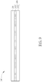
- FIG. 9 is a cross-sectional schematic diagram of a structure of a display device according to a third embodiment of the present disclosure
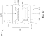
- FIG. 10 is a partial-enlargement schematic diagram illustrating a cross-section of the display device shown in FIG. 9
- the display device 100' in this embodiment is a self-luminous display device and includes a display substrate 200, wherein the display substrate 200 may include the substrate 1021 and the light emitting array layer 1022 as mentioned in the above embodiments or variant embodiments.
- the light emitting array layer 1022 in this embodiment includes a plurality of light emitting units LU arranged in an array, and each light emitting unit LU includes at least two driving arrays and at least one light emitting element LE disposed on the surface of the substrate 1021, wherein the included elements, the arrangement and the electrical connection relationship of each of the light emitting units LU may refer to the above description and will not be described redundantly.
- the light emitting element LE of this embodiment may be an OLED, but not limited thereto.
- the light emitting element LE may be other suitable elements, such as mini LED and micro LED. As shown in FIG.
- the light emitting element LE includes a first terminal LE1, a second terminal LE2 and a light emitting layer LE3, wherein the first terminal LE1 and the second terminal LE2 may respectively serve as the anode and the cathode of the light emitting element LE.
- a second transistor TFT2 in the same light emitting unit LU disposed on the substrate 1021 is illustrated in FIG. 10 , while other transistors that may exist in the light emitting unit LU are omitted in FIG. 10 .
- the second transistor TFT2 in this embodiment is a top-gate type thin film transistor as an example; however, the second transistor TFT2 may be a bottom-gate type thin film transistor in a variant embodiment.
- one light emitting unit LU may be considered as one sub pixel PX of the display device 100'.
- the brightness of the light emitting element LE of each sub pixel PX may be controlled by the corresponding scan line and data line, and each sub pixel PX may have a light emitting element LE with non-identified color disposed therein as needed, so as to display colorful images.
- one light emitting unit LU includes more than one light emitting elements LE, all of the plural light emitting elements LE in one single light emitting unit LU may have the same color.
- the display device 100' in this embodiment may further include another substrate 106 disposed on the light emitting array layer 1022 to provide protection.
- the another substrate 106 may also be a protection layer (such as a barrier layer), a glass or an inorganic-organic-inorganic (IOI) packaging layer without particular limitation, which has a mainly function of protecting the light emitting array or blocking moisture and oxygen.
- a protection layer such as a barrier layer
- a glass or an inorganic-organic-inorganic (IOI) packaging layer without particular limitation, which has a mainly function of protecting the light emitting array or blocking moisture and oxygen.
- the substrate of the present disclosure that has the driving arrays and the light emitting elements disposed thereon may serve as a backlight source of the display panel in some embodiments; while the substrate itself may serve as the display panel that can produce one single color or multiple colors to display images in some other embodiments.
- the display device or the display substrate in the present disclosure has two or more driving arrays corresponding to the same light emitting element disposed on the substrate. When one of the driving arrays is failed, another driving array that functions normally may be selected to be electrically connected to the light emitting element, such that the light emitting element can emit light normally and the whole light emitting unit may function effectively.
- the driving unit in the present disclosure has a driving transistor with four terminal electrodes (i.e., the second transistor mentioned above), which may increase the stability of the transistor and/or may additionally improve the light uniformity of the display substrate.
Landscapes
- Engineering & Computer Science (AREA)
- Physics & Mathematics (AREA)
- Computer Hardware Design (AREA)
- General Physics & Mathematics (AREA)
- Theoretical Computer Science (AREA)
- Chemical & Material Sciences (AREA)
- Crystallography & Structural Chemistry (AREA)
- Microelectronics & Electronic Packaging (AREA)
- Electroluminescent Light Sources (AREA)
- Devices For Indicating Variable Information By Combining Individual Elements (AREA)
Priority Applications (1)
| Application Number | Priority Date | Filing Date | Title |
|---|---|---|---|
| EP23186882.9A EP4254392A3 (de) | 2018-04-19 | 2019-04-01 | Anzeigetafel und verfahren zur herstellung eines anzeigesubstrat |
Applications Claiming Priority (2)
| Application Number | Priority Date | Filing Date | Title |
|---|---|---|---|
| US201862659712P | 2018-04-19 | 2018-04-19 | |
| CN201810427605.7A CN110400543A (zh) | 2018-04-19 | 2018-05-07 | 显示设备 |
Related Child Applications (2)
| Application Number | Title | Priority Date | Filing Date |
|---|---|---|---|
| EP23186882.9A Division EP4254392A3 (de) | 2018-04-19 | 2019-04-01 | Anzeigetafel und verfahren zur herstellung eines anzeigesubstrat |
| EP23186882.9A Division-Into EP4254392A3 (de) | 2018-04-19 | 2019-04-01 | Anzeigetafel und verfahren zur herstellung eines anzeigesubstrat |
Publications (2)
| Publication Number | Publication Date |
|---|---|
| EP3557565A1 true EP3557565A1 (de) | 2019-10-23 |
| EP3557565B1 EP3557565B1 (de) | 2023-09-06 |
Family
ID=66049019
Family Applications (2)
| Application Number | Title | Priority Date | Filing Date |
|---|---|---|---|
| EP23186882.9A Withdrawn EP4254392A3 (de) | 2018-04-19 | 2019-04-01 | Anzeigetafel und verfahren zur herstellung eines anzeigesubstrat |
| EP19166452.3A Active EP3557565B1 (de) | 2018-04-19 | 2019-04-01 | Anzeigetafel und verfahren zur herstellung eines anzeigesubstrat |
Family Applications Before (1)
| Application Number | Title | Priority Date | Filing Date |
|---|---|---|---|
| EP23186882.9A Withdrawn EP4254392A3 (de) | 2018-04-19 | 2019-04-01 | Anzeigetafel und verfahren zur herstellung eines anzeigesubstrat |
Country Status (2)
| Country | Link |
|---|---|
| US (1) | US10930196B2 (de) |
| EP (2) | EP4254392A3 (de) |
Families Citing this family (1)
| Publication number | Priority date | Publication date | Assignee | Title |
|---|---|---|---|---|
| TWI806538B (zh) * | 2022-04-07 | 2023-06-21 | 友達光電股份有限公司 | 顯示裝置 |
Citations (2)
| Publication number | Priority date | Publication date | Assignee | Title |
|---|---|---|---|---|
| US20040066146A1 (en) * | 2002-07-16 | 2004-04-08 | Lg.Philips Lcd Co., Ltd. | Organic electroluminescent device having backup driving unit |
| EP3163559A1 (de) * | 2014-06-27 | 2017-05-03 | BOE Technology Group Co., Ltd. | Pixelschaltung, anzeigetafel und anzeigevorrichtung |
Family Cites Families (10)
| Publication number | Priority date | Publication date | Assignee | Title |
|---|---|---|---|---|
| US8698706B1 (en) | 2001-10-23 | 2014-04-15 | Imaging Systems Technology, Inc. | Organic electroluminescent display device driving method and apparatus |
| GB0226401D0 (en) * | 2002-11-12 | 2002-12-18 | Koninkl Philips Electronics Nv | Electroluminescent devices and their manufacture |
| TWI328213B (en) * | 2005-12-16 | 2010-08-01 | Chi Mei El Corp | Plate display and pixel circuitry |
| TW200725073A (en) * | 2005-12-23 | 2007-07-01 | Innolux Display Corp | Liquid crystal display device |
| TWI356386B (en) * | 2006-08-04 | 2012-01-11 | Ritdisplay Corp | Active matrix organic electro-luminescence display |
| KR20110098845A (ko) * | 2008-12-23 | 2011-09-01 | 프라운호퍼 게젤샤프트 쭈르 푀르데룽 데어 안겐반텐 포르슝 에. 베. | 인간에 대한 일주 효력을 가지는 디스플레이 시스템 |
| CN106663406A (zh) * | 2014-06-05 | 2017-05-10 | 寇平公司 | 有源矩阵led像素驱动电路和布局方法 |
| KR102203999B1 (ko) * | 2014-07-08 | 2021-01-19 | 삼성디스플레이 주식회사 | 유기 발광 표시 패널 및 이를 포함하는 유기 발광 표시 장치 |
| US10181284B2 (en) * | 2015-03-13 | 2019-01-15 | Boe Technology Group Co., Ltd. | Pixel driving circuit and repairing method thereof and display apparatus |
| CN107591125A (zh) * | 2017-10-26 | 2018-01-16 | 京东方科技集团股份有限公司 | 一种电致发光元件的驱动电路和驱动方法、显示装置 |
-
2019
- 2019-03-25 US US16/364,154 patent/US10930196B2/en active Active
- 2019-04-01 EP EP23186882.9A patent/EP4254392A3/de not_active Withdrawn
- 2019-04-01 EP EP19166452.3A patent/EP3557565B1/de active Active
Patent Citations (2)
| Publication number | Priority date | Publication date | Assignee | Title |
|---|---|---|---|---|
| US20040066146A1 (en) * | 2002-07-16 | 2004-04-08 | Lg.Philips Lcd Co., Ltd. | Organic electroluminescent device having backup driving unit |
| EP3163559A1 (de) * | 2014-06-27 | 2017-05-03 | BOE Technology Group Co., Ltd. | Pixelschaltung, anzeigetafel und anzeigevorrichtung |
Also Published As
| Publication number | Publication date |
|---|---|
| EP4254392A3 (de) | 2023-11-15 |
| US20190325807A1 (en) | 2019-10-24 |
| EP3557565B1 (de) | 2023-09-06 |
| US10930196B2 (en) | 2021-02-23 |
| EP4254392A2 (de) | 2023-10-04 |
Similar Documents
| Publication | Publication Date | Title |
|---|---|---|
| KR102763273B1 (ko) | 디스플레이 장치 | |
| US11315454B2 (en) | Display device | |
| EP3934383B1 (de) | Substrat für lichtemissionssubstrat, anzeigevorrichtung und verfahren zur reparatur einer anzeigevorrichtung | |
| KR100884455B1 (ko) | 유기전계발광 표시장치 및 그 모기판 | |
| US9214479B2 (en) | Light emitting diode display panel | |
| WO2018120754A1 (zh) | Oled阵列基板、显示装置及其暗点修复方法 | |
| KR102702297B1 (ko) | 표시 장치 | |
| KR20190053347A (ko) | 엘이디 구동 유닛들이 형성된 tft 기판을 갖는 엘이디 디스플레이 장치 | |
| US9361820B2 (en) | Apparatus and method for inspecting short circuit defects | |
| US7888683B2 (en) | Organic light emitting display and method for making the same | |
| KR102013319B1 (ko) | 평판 표시 장치 및 이의 제조 방법 | |
| US20160358533A1 (en) | Self-compensating circuit for faulty display pixels | |
| CN102447075B (zh) | 显示面板 | |
| KR20160082883A (ko) | 디스플레이 장치 | |
| US20110157114A1 (en) | Electroluminescence device | |
| US9405162B2 (en) | Active matrix display device with auxiliary repair line | |
| JP7326470B2 (ja) | 表示装置 | |
| CN110689818B (zh) | 电子装置及电子装置的修复方法 | |
| US11195828B2 (en) | Semiconductor device | |
| KR20140118005A (ko) | 유기 발광 표시 장치 및 그 제조 방법 | |
| EP3557565B1 (de) | Anzeigetafel und verfahren zur herstellung eines anzeigesubstrat | |
| KR20230033251A (ko) | 표시 장치 | |
| KR102463349B1 (ko) | 표시장치 | |
| CN110400543A (zh) | 显示设备 | |
| US20260075705A1 (en) | Mother board for display device and display device |
Legal Events
| Date | Code | Title | Description |
|---|---|---|---|
| PUAI | Public reference made under article 153(3) epc to a published international application that has entered the european phase |
Free format text: ORIGINAL CODE: 0009012 |
|
| STAA | Information on the status of an ep patent application or granted ep patent |
Free format text: STATUS: THE APPLICATION HAS BEEN PUBLISHED |
|
| AK | Designated contracting states |
Kind code of ref document: A1 Designated state(s): AL AT BE BG CH CY CZ DE DK EE ES FI FR GB GR HR HU IE IS IT LI LT LU LV MC MK MT NL NO PL PT RO RS SE SI SK SM TR |
|
| AX | Request for extension of the european patent |
Extension state: BA ME |
|
| STAA | Information on the status of an ep patent application or granted ep patent |
Free format text: STATUS: REQUEST FOR EXAMINATION WAS MADE |
|
| 17P | Request for examination filed |
Effective date: 20200422 |
|
| RBV | Designated contracting states (corrected) |
Designated state(s): AL AT BE BG CH CY CZ DE DK EE ES FI FR GB GR HR HU IE IS IT LI LT LU LV MC MK MT NL NO PL PT RO RS SE SI SK SM TR |
|
| STAA | Information on the status of an ep patent application or granted ep patent |
Free format text: STATUS: EXAMINATION IS IN PROGRESS |
|
| 17Q | First examination report despatched |
Effective date: 20201104 |
|
| GRAP | Despatch of communication of intention to grant a patent |
Free format text: ORIGINAL CODE: EPIDOSNIGR1 |
|
| STAA | Information on the status of an ep patent application or granted ep patent |
Free format text: STATUS: GRANT OF PATENT IS INTENDED |
|
| RIC1 | Information provided on ipc code assigned before grant |
Ipc: G09G 3/3233 20160101ALI20230307BHEP Ipc: G09G 3/34 20060101ALI20230307BHEP Ipc: G09G 3/36 20060101ALI20230307BHEP Ipc: G09G 3/20 20060101AFI20230307BHEP |
|
| INTG | Intention to grant announced |
Effective date: 20230330 |
|
| GRAS | Grant fee paid |
Free format text: ORIGINAL CODE: EPIDOSNIGR3 |
|
| GRAA | (expected) grant |
Free format text: ORIGINAL CODE: 0009210 |
|
| STAA | Information on the status of an ep patent application or granted ep patent |
Free format text: STATUS: THE PATENT HAS BEEN GRANTED |
|
| AK | Designated contracting states |
Kind code of ref document: B1 Designated state(s): AL AT BE BG CH CY CZ DE DK EE ES FI FR GB GR HR HU IE IS IT LI LT LU LV MC MK MT NL NO PL PT RO RS SE SI SK SM TR |
|
| REG | Reference to a national code |
Ref country code: GB Ref legal event code: FG4D |
|
| REG | Reference to a national code |
Ref country code: CH Ref legal event code: EP |
|
| REG | Reference to a national code |
Ref country code: DE Ref legal event code: R096 Ref document number: 602019036577 Country of ref document: DE |
|
| REG | Reference to a national code |
Ref country code: IE Ref legal event code: FG4D |
|
| REG | Reference to a national code |
Ref country code: LT Ref legal event code: MG9D |
|
| REG | Reference to a national code |
Ref country code: NL Ref legal event code: MP Effective date: 20230906 |
|
| PG25 | Lapsed in a contracting state [announced via postgrant information from national office to epo] |
Ref country code: GR Free format text: LAPSE BECAUSE OF FAILURE TO SUBMIT A TRANSLATION OF THE DESCRIPTION OR TO PAY THE FEE WITHIN THE PRESCRIBED TIME-LIMIT Effective date: 20231207 |
|
| PG25 | Lapsed in a contracting state [announced via postgrant information from national office to epo] |
Ref country code: SE Free format text: LAPSE BECAUSE OF FAILURE TO SUBMIT A TRANSLATION OF THE DESCRIPTION OR TO PAY THE FEE WITHIN THE PRESCRIBED TIME-LIMIT Effective date: 20230906 Ref country code: RS Free format text: LAPSE BECAUSE OF FAILURE TO SUBMIT A TRANSLATION OF THE DESCRIPTION OR TO PAY THE FEE WITHIN THE PRESCRIBED TIME-LIMIT Effective date: 20230906 Ref country code: NO Free format text: LAPSE BECAUSE OF FAILURE TO SUBMIT A TRANSLATION OF THE DESCRIPTION OR TO PAY THE FEE WITHIN THE PRESCRIBED TIME-LIMIT Effective date: 20231206 Ref country code: LV Free format text: LAPSE BECAUSE OF FAILURE TO SUBMIT A TRANSLATION OF THE DESCRIPTION OR TO PAY THE FEE WITHIN THE PRESCRIBED TIME-LIMIT Effective date: 20230906 Ref country code: LT Free format text: LAPSE BECAUSE OF FAILURE TO SUBMIT A TRANSLATION OF THE DESCRIPTION OR TO PAY THE FEE WITHIN THE PRESCRIBED TIME-LIMIT Effective date: 20230906 Ref country code: HR Free format text: LAPSE BECAUSE OF FAILURE TO SUBMIT A TRANSLATION OF THE DESCRIPTION OR TO PAY THE FEE WITHIN THE PRESCRIBED TIME-LIMIT Effective date: 20230906 Ref country code: GR Free format text: LAPSE BECAUSE OF FAILURE TO SUBMIT A TRANSLATION OF THE DESCRIPTION OR TO PAY THE FEE WITHIN THE PRESCRIBED TIME-LIMIT Effective date: 20231207 Ref country code: FI Free format text: LAPSE BECAUSE OF FAILURE TO SUBMIT A TRANSLATION OF THE DESCRIPTION OR TO PAY THE FEE WITHIN THE PRESCRIBED TIME-LIMIT Effective date: 20230906 |
|
| REG | Reference to a national code |
Ref country code: AT Ref legal event code: MK05 Ref document number: 1609608 Country of ref document: AT Kind code of ref document: T Effective date: 20230906 |
|
| PG25 | Lapsed in a contracting state [announced via postgrant information from national office to epo] |
Ref country code: NL Free format text: LAPSE BECAUSE OF FAILURE TO SUBMIT A TRANSLATION OF THE DESCRIPTION OR TO PAY THE FEE WITHIN THE PRESCRIBED TIME-LIMIT Effective date: 20230906 |
|
| PG25 | Lapsed in a contracting state [announced via postgrant information from national office to epo] |
Ref country code: IS Free format text: LAPSE BECAUSE OF FAILURE TO SUBMIT A TRANSLATION OF THE DESCRIPTION OR TO PAY THE FEE WITHIN THE PRESCRIBED TIME-LIMIT Effective date: 20240106 |
|
| PG25 | Lapsed in a contracting state [announced via postgrant information from national office to epo] |
Ref country code: AT Free format text: LAPSE BECAUSE OF FAILURE TO SUBMIT A TRANSLATION OF THE DESCRIPTION OR TO PAY THE FEE WITHIN THE PRESCRIBED TIME-LIMIT Effective date: 20230906 |
|
| PG25 | Lapsed in a contracting state [announced via postgrant information from national office to epo] |
Ref country code: ES Free format text: LAPSE BECAUSE OF FAILURE TO SUBMIT A TRANSLATION OF THE DESCRIPTION OR TO PAY THE FEE WITHIN THE PRESCRIBED TIME-LIMIT Effective date: 20230906 |
|
| PG25 | Lapsed in a contracting state [announced via postgrant information from national office to epo] |
Ref country code: SM Free format text: LAPSE BECAUSE OF FAILURE TO SUBMIT A TRANSLATION OF THE DESCRIPTION OR TO PAY THE FEE WITHIN THE PRESCRIBED TIME-LIMIT Effective date: 20230906 Ref country code: RO Free format text: LAPSE BECAUSE OF FAILURE TO SUBMIT A TRANSLATION OF THE DESCRIPTION OR TO PAY THE FEE WITHIN THE PRESCRIBED TIME-LIMIT Effective date: 20230906 Ref country code: IS Free format text: LAPSE BECAUSE OF FAILURE TO SUBMIT A TRANSLATION OF THE DESCRIPTION OR TO PAY THE FEE WITHIN THE PRESCRIBED TIME-LIMIT Effective date: 20240106 Ref country code: ES Free format text: LAPSE BECAUSE OF FAILURE TO SUBMIT A TRANSLATION OF THE DESCRIPTION OR TO PAY THE FEE WITHIN THE PRESCRIBED TIME-LIMIT Effective date: 20230906 Ref country code: EE Free format text: LAPSE BECAUSE OF FAILURE TO SUBMIT A TRANSLATION OF THE DESCRIPTION OR TO PAY THE FEE WITHIN THE PRESCRIBED TIME-LIMIT Effective date: 20230906 Ref country code: CZ Free format text: LAPSE BECAUSE OF FAILURE TO SUBMIT A TRANSLATION OF THE DESCRIPTION OR TO PAY THE FEE WITHIN THE PRESCRIBED TIME-LIMIT Effective date: 20230906 Ref country code: AT Free format text: LAPSE BECAUSE OF FAILURE TO SUBMIT A TRANSLATION OF THE DESCRIPTION OR TO PAY THE FEE WITHIN THE PRESCRIBED TIME-LIMIT Effective date: 20230906 Ref country code: PT Free format text: LAPSE BECAUSE OF FAILURE TO SUBMIT A TRANSLATION OF THE DESCRIPTION OR TO PAY THE FEE WITHIN THE PRESCRIBED TIME-LIMIT Effective date: 20240108 Ref country code: SK Free format text: LAPSE BECAUSE OF FAILURE TO SUBMIT A TRANSLATION OF THE DESCRIPTION OR TO PAY THE FEE WITHIN THE PRESCRIBED TIME-LIMIT Effective date: 20230906 |
|
| PG25 | Lapsed in a contracting state [announced via postgrant information from national office to epo] |
Ref country code: PL Free format text: LAPSE BECAUSE OF FAILURE TO SUBMIT A TRANSLATION OF THE DESCRIPTION OR TO PAY THE FEE WITHIN THE PRESCRIBED TIME-LIMIT Effective date: 20230906 Ref country code: IT Free format text: LAPSE BECAUSE OF FAILURE TO SUBMIT A TRANSLATION OF THE DESCRIPTION OR TO PAY THE FEE WITHIN THE PRESCRIBED TIME-LIMIT Effective date: 20230906 |
|
| REG | Reference to a national code |
Ref country code: DE Ref legal event code: R097 Ref document number: 602019036577 Country of ref document: DE |
|
| PG25 | Lapsed in a contracting state [announced via postgrant information from national office to epo] |
Ref country code: DK Free format text: LAPSE BECAUSE OF FAILURE TO SUBMIT A TRANSLATION OF THE DESCRIPTION OR TO PAY THE FEE WITHIN THE PRESCRIBED TIME-LIMIT Effective date: 20230906 |
|
| PLBE | No opposition filed within time limit |
Free format text: ORIGINAL CODE: 0009261 |
|
| STAA | Information on the status of an ep patent application or granted ep patent |
Free format text: STATUS: NO OPPOSITION FILED WITHIN TIME LIMIT |
|
| PG25 | Lapsed in a contracting state [announced via postgrant information from national office to epo] |
Ref country code: DK Free format text: LAPSE BECAUSE OF FAILURE TO SUBMIT A TRANSLATION OF THE DESCRIPTION OR TO PAY THE FEE WITHIN THE PRESCRIBED TIME-LIMIT Effective date: 20230906 Ref country code: SI Free format text: LAPSE BECAUSE OF FAILURE TO SUBMIT A TRANSLATION OF THE DESCRIPTION OR TO PAY THE FEE WITHIN THE PRESCRIBED TIME-LIMIT Effective date: 20230906 |
|
| 26N | No opposition filed |
Effective date: 20240607 |
|
| REG | Reference to a national code |
Ref country code: DE Ref legal event code: R082 Ref document number: 602019036577 Country of ref document: DE Representative=s name: STRAUS, ALEXANDER, DIPL.-CHEM.UNIV. DR.PHIL., DE |
|
| PG25 | Lapsed in a contracting state [announced via postgrant information from national office to epo] |
Ref country code: BG Free format text: LAPSE BECAUSE OF FAILURE TO SUBMIT A TRANSLATION OF THE DESCRIPTION OR TO PAY THE FEE WITHIN THE PRESCRIBED TIME-LIMIT Effective date: 20230906 |
|
| PG25 | Lapsed in a contracting state [announced via postgrant information from national office to epo] |
Ref country code: MC Free format text: LAPSE BECAUSE OF FAILURE TO SUBMIT A TRANSLATION OF THE DESCRIPTION OR TO PAY THE FEE WITHIN THE PRESCRIBED TIME-LIMIT Effective date: 20230906 |
|
| PG25 | Lapsed in a contracting state [announced via postgrant information from national office to epo] |
Ref country code: MC Free format text: LAPSE BECAUSE OF FAILURE TO SUBMIT A TRANSLATION OF THE DESCRIPTION OR TO PAY THE FEE WITHIN THE PRESCRIBED TIME-LIMIT Effective date: 20230906 Ref country code: BG Free format text: LAPSE BECAUSE OF FAILURE TO SUBMIT A TRANSLATION OF THE DESCRIPTION OR TO PAY THE FEE WITHIN THE PRESCRIBED TIME-LIMIT Effective date: 20230906 |
|
| REG | Reference to a national code |
Ref country code: CH Ref legal event code: PL |
|
| PG25 | Lapsed in a contracting state [announced via postgrant information from national office to epo] |
Ref country code: LU Free format text: LAPSE BECAUSE OF NON-PAYMENT OF DUE FEES Effective date: 20240401 |
|
| REG | Reference to a national code |
Ref country code: BE Ref legal event code: MM Effective date: 20240430 |
|
| PG25 | Lapsed in a contracting state [announced via postgrant information from national office to epo] |
Ref country code: LU Free format text: LAPSE BECAUSE OF NON-PAYMENT OF DUE FEES Effective date: 20240401 |
|
| PG25 | Lapsed in a contracting state [announced via postgrant information from national office to epo] |
Ref country code: BE Free format text: LAPSE BECAUSE OF NON-PAYMENT OF DUE FEES Effective date: 20240430 |
|
| PG25 | Lapsed in a contracting state [announced via postgrant information from national office to epo] |
Ref country code: BE Free format text: LAPSE BECAUSE OF NON-PAYMENT OF DUE FEES Effective date: 20240430 Ref country code: CH Free format text: LAPSE BECAUSE OF NON-PAYMENT OF DUE FEES Effective date: 20240430 |
|
| PG25 | Lapsed in a contracting state [announced via postgrant information from national office to epo] |
Ref country code: IE Free format text: LAPSE BECAUSE OF NON-PAYMENT OF DUE FEES Effective date: 20240401 |
|
| PGFP | Annual fee paid to national office [announced via postgrant information from national office to epo] |
Ref country code: DE Payment date: 20250402 Year of fee payment: 7 |
|
| PGFP | Annual fee paid to national office [announced via postgrant information from national office to epo] |
Ref country code: FR Payment date: 20250401 Year of fee payment: 7 |
|
| PG25 | Lapsed in a contracting state [announced via postgrant information from national office to epo] |
Ref country code: CY Free format text: LAPSE BECAUSE OF FAILURE TO SUBMIT A TRANSLATION OF THE DESCRIPTION OR TO PAY THE FEE WITHIN THE PRESCRIBED TIME-LIMIT; INVALID AB INITIO Effective date: 20190401 |
|
| PG25 | Lapsed in a contracting state [announced via postgrant information from national office to epo] |
Ref country code: HU Free format text: LAPSE BECAUSE OF FAILURE TO SUBMIT A TRANSLATION OF THE DESCRIPTION OR TO PAY THE FEE WITHIN THE PRESCRIBED TIME-LIMIT; INVALID AB INITIO Effective date: 20190401 |
|
| PG25 | Lapsed in a contracting state [announced via postgrant information from national office to epo] |
Ref country code: TR Free format text: LAPSE BECAUSE OF FAILURE TO SUBMIT A TRANSLATION OF THE DESCRIPTION OR TO PAY THE FEE WITHIN THE PRESCRIBED TIME-LIMIT Effective date: 20230906 |
|
| PGFP | Annual fee paid to national office [announced via postgrant information from national office to epo] |
Ref country code: GB Payment date: 20260324 Year of fee payment: 8 |