EP3556912B1 - Group iii nitride semiconductor substrate and production method for group iii nitride semiconductor substrate - Google Patents
Group iii nitride semiconductor substrate and production method for group iii nitride semiconductor substrate Download PDFInfo
- Publication number
- EP3556912B1 EP3556912B1 EP17885108.5A EP17885108A EP3556912B1 EP 3556912 B1 EP3556912 B1 EP 3556912B1 EP 17885108 A EP17885108 A EP 17885108A EP 3556912 B1 EP3556912 B1 EP 3556912B1
- Authority
- EP
- European Patent Office
- Prior art keywords
- nitride semiconductor
- group iii
- iii nitride
- plane
- semiconductor layer
- Prior art date
- Legal status (The legal status is an assumption and is not a legal conclusion. Google has not performed a legal analysis and makes no representation as to the accuracy of the status listed.)
- Active
Links
Images






Classifications
-
- C—CHEMISTRY; METALLURGY
- C30—CRYSTAL GROWTH
- C30B—SINGLE-CRYSTAL GROWTH; UNIDIRECTIONAL SOLIDIFICATION OF EUTECTIC MATERIAL OR UNIDIRECTIONAL DEMIXING OF EUTECTOID MATERIAL; REFINING BY ZONE-MELTING OF MATERIAL; PRODUCTION OF A HOMOGENEOUS POLYCRYSTALLINE MATERIAL WITH DEFINED STRUCTURE; SINGLE CRYSTALS OR HOMOGENEOUS POLYCRYSTALLINE MATERIAL WITH DEFINED STRUCTURE; AFTER-TREATMENT OF SINGLE CRYSTALS OR A HOMOGENEOUS POLYCRYSTALLINE MATERIAL WITH DEFINED STRUCTURE; APPARATUS THEREFOR
- C30B29/00—Single crystals or homogeneous polycrystalline material with defined structure characterised by the material or by their shape
- C30B29/10—Inorganic compounds or compositions
- C30B29/40—AIIIBV compounds wherein A is B, Al, Ga, In or Tl and B is N, P, As, Sb or Bi
- C30B29/403—AIII-nitrides
- C30B29/406—Gallium nitride
-
- C—CHEMISTRY; METALLURGY
- C30—CRYSTAL GROWTH
- C30B—SINGLE-CRYSTAL GROWTH; UNIDIRECTIONAL SOLIDIFICATION OF EUTECTIC MATERIAL OR UNIDIRECTIONAL DEMIXING OF EUTECTOID MATERIAL; REFINING BY ZONE-MELTING OF MATERIAL; PRODUCTION OF A HOMOGENEOUS POLYCRYSTALLINE MATERIAL WITH DEFINED STRUCTURE; SINGLE CRYSTALS OR HOMOGENEOUS POLYCRYSTALLINE MATERIAL WITH DEFINED STRUCTURE; AFTER-TREATMENT OF SINGLE CRYSTALS OR A HOMOGENEOUS POLYCRYSTALLINE MATERIAL WITH DEFINED STRUCTURE; APPARATUS THEREFOR
- C30B25/00—Single-crystal growth by chemical reaction of reactive gases, e.g. chemical vapour-deposition growth
- C30B25/02—Epitaxial-layer growth
- C30B25/18—Epitaxial-layer growth characterised by the substrate
-
- H—ELECTRICITY
- H10—SEMICONDUCTOR DEVICES; ELECTRIC SOLID-STATE DEVICES NOT OTHERWISE PROVIDED FOR
- H10D—INORGANIC ELECTRIC SEMICONDUCTOR DEVICES
- H10D62/00—Semiconductor bodies, or regions thereof, of devices having potential barriers
- H10D62/80—Semiconductor bodies, or regions thereof, of devices having potential barriers characterised by the materials
- H10D62/85—Semiconductor bodies, or regions thereof, of devices having potential barriers characterised by the materials being Group III-V materials, e.g. GaAs
- H10D62/8503—Nitride Group III-V materials, e.g. AlN or GaN
-
- C—CHEMISTRY; METALLURGY
- C23—COATING METALLIC MATERIAL; COATING MATERIAL WITH METALLIC MATERIAL; CHEMICAL SURFACE TREATMENT; DIFFUSION TREATMENT OF METALLIC MATERIAL; COATING BY VACUUM EVAPORATION, BY SPUTTERING, BY ION IMPLANTATION OR BY CHEMICAL VAPOUR DEPOSITION, IN GENERAL; INHIBITING CORROSION OF METALLIC MATERIAL OR INCRUSTATION IN GENERAL
- C23C—COATING METALLIC MATERIAL; COATING MATERIAL WITH METALLIC MATERIAL; SURFACE TREATMENT OF METALLIC MATERIAL BY DIFFUSION INTO THE SURFACE, BY CHEMICAL CONVERSION OR SUBSTITUTION; COATING BY VACUUM EVAPORATION, BY SPUTTERING, BY ION IMPLANTATION OR BY CHEMICAL VAPOUR DEPOSITION, IN GENERAL
- C23C16/00—Chemical coating by decomposition of gaseous compounds, without leaving reaction products of surface material in the coating, i.e. chemical vapour deposition [CVD] processes
- C23C16/02—Pretreatment of the material to be coated
- C23C16/0209—Pretreatment of the material to be coated by heating
-
- C—CHEMISTRY; METALLURGY
- C23—COATING METALLIC MATERIAL; COATING MATERIAL WITH METALLIC MATERIAL; CHEMICAL SURFACE TREATMENT; DIFFUSION TREATMENT OF METALLIC MATERIAL; COATING BY VACUUM EVAPORATION, BY SPUTTERING, BY ION IMPLANTATION OR BY CHEMICAL VAPOUR DEPOSITION, IN GENERAL; INHIBITING CORROSION OF METALLIC MATERIAL OR INCRUSTATION IN GENERAL
- C23C—COATING METALLIC MATERIAL; COATING MATERIAL WITH METALLIC MATERIAL; SURFACE TREATMENT OF METALLIC MATERIAL BY DIFFUSION INTO THE SURFACE, BY CHEMICAL CONVERSION OR SUBSTITUTION; COATING BY VACUUM EVAPORATION, BY SPUTTERING, BY ION IMPLANTATION OR BY CHEMICAL VAPOUR DEPOSITION, IN GENERAL
- C23C16/00—Chemical coating by decomposition of gaseous compounds, without leaving reaction products of surface material in the coating, i.e. chemical vapour deposition [CVD] processes
- C23C16/02—Pretreatment of the material to be coated
- C23C16/0272—Deposition of sub-layers, e.g. to promote the adhesion of the main coating
-
- C—CHEMISTRY; METALLURGY
- C23—COATING METALLIC MATERIAL; COATING MATERIAL WITH METALLIC MATERIAL; CHEMICAL SURFACE TREATMENT; DIFFUSION TREATMENT OF METALLIC MATERIAL; COATING BY VACUUM EVAPORATION, BY SPUTTERING, BY ION IMPLANTATION OR BY CHEMICAL VAPOUR DEPOSITION, IN GENERAL; INHIBITING CORROSION OF METALLIC MATERIAL OR INCRUSTATION IN GENERAL
- C23C—COATING METALLIC MATERIAL; COATING MATERIAL WITH METALLIC MATERIAL; SURFACE TREATMENT OF METALLIC MATERIAL BY DIFFUSION INTO THE SURFACE, BY CHEMICAL CONVERSION OR SUBSTITUTION; COATING BY VACUUM EVAPORATION, BY SPUTTERING, BY ION IMPLANTATION OR BY CHEMICAL VAPOUR DEPOSITION, IN GENERAL
- C23C16/00—Chemical coating by decomposition of gaseous compounds, without leaving reaction products of surface material in the coating, i.e. chemical vapour deposition [CVD] processes
- C23C16/22—Chemical coating by decomposition of gaseous compounds, without leaving reaction products of surface material in the coating, i.e. chemical vapour deposition [CVD] processes characterised by the deposition of inorganic material, other than metallic material
- C23C16/30—Deposition of compounds, mixtures or solid solutions, e.g. borides, carbides, nitrides
- C23C16/301—AIII BV compounds, where A is Al, Ga, In or Tl and B is N, P, As, Sb or Bi
- C23C16/303—Nitrides
-
- C—CHEMISTRY; METALLURGY
- C23—COATING METALLIC MATERIAL; COATING MATERIAL WITH METALLIC MATERIAL; CHEMICAL SURFACE TREATMENT; DIFFUSION TREATMENT OF METALLIC MATERIAL; COATING BY VACUUM EVAPORATION, BY SPUTTERING, BY ION IMPLANTATION OR BY CHEMICAL VAPOUR DEPOSITION, IN GENERAL; INHIBITING CORROSION OF METALLIC MATERIAL OR INCRUSTATION IN GENERAL
- C23C—COATING METALLIC MATERIAL; COATING MATERIAL WITH METALLIC MATERIAL; SURFACE TREATMENT OF METALLIC MATERIAL BY DIFFUSION INTO THE SURFACE, BY CHEMICAL CONVERSION OR SUBSTITUTION; COATING BY VACUUM EVAPORATION, BY SPUTTERING, BY ION IMPLANTATION OR BY CHEMICAL VAPOUR DEPOSITION, IN GENERAL
- C23C16/00—Chemical coating by decomposition of gaseous compounds, without leaving reaction products of surface material in the coating, i.e. chemical vapour deposition [CVD] processes
- C23C16/22—Chemical coating by decomposition of gaseous compounds, without leaving reaction products of surface material in the coating, i.e. chemical vapour deposition [CVD] processes characterised by the deposition of inorganic material, other than metallic material
- C23C16/30—Deposition of compounds, mixtures or solid solutions, e.g. borides, carbides, nitrides
- C23C16/34—Nitrides
-
- C—CHEMISTRY; METALLURGY
- C30—CRYSTAL GROWTH
- C30B—SINGLE-CRYSTAL GROWTH; UNIDIRECTIONAL SOLIDIFICATION OF EUTECTIC MATERIAL OR UNIDIRECTIONAL DEMIXING OF EUTECTOID MATERIAL; REFINING BY ZONE-MELTING OF MATERIAL; PRODUCTION OF A HOMOGENEOUS POLYCRYSTALLINE MATERIAL WITH DEFINED STRUCTURE; SINGLE CRYSTALS OR HOMOGENEOUS POLYCRYSTALLINE MATERIAL WITH DEFINED STRUCTURE; AFTER-TREATMENT OF SINGLE CRYSTALS OR A HOMOGENEOUS POLYCRYSTALLINE MATERIAL WITH DEFINED STRUCTURE; APPARATUS THEREFOR
- C30B25/00—Single-crystal growth by chemical reaction of reactive gases, e.g. chemical vapour-deposition growth
- C30B25/02—Epitaxial-layer growth
- C30B25/18—Epitaxial-layer growth characterised by the substrate
- C30B25/183—Epitaxial-layer growth characterised by the substrate being provided with a buffer layer, e.g. a lattice matching layer
-
- C—CHEMISTRY; METALLURGY
- C30—CRYSTAL GROWTH
- C30B—SINGLE-CRYSTAL GROWTH; UNIDIRECTIONAL SOLIDIFICATION OF EUTECTIC MATERIAL OR UNIDIRECTIONAL DEMIXING OF EUTECTOID MATERIAL; REFINING BY ZONE-MELTING OF MATERIAL; PRODUCTION OF A HOMOGENEOUS POLYCRYSTALLINE MATERIAL WITH DEFINED STRUCTURE; SINGLE CRYSTALS OR HOMOGENEOUS POLYCRYSTALLINE MATERIAL WITH DEFINED STRUCTURE; AFTER-TREATMENT OF SINGLE CRYSTALS OR A HOMOGENEOUS POLYCRYSTALLINE MATERIAL WITH DEFINED STRUCTURE; APPARATUS THEREFOR
- C30B25/00—Single-crystal growth by chemical reaction of reactive gases, e.g. chemical vapour-deposition growth
- C30B25/02—Epitaxial-layer growth
- C30B25/18—Epitaxial-layer growth characterised by the substrate
- C30B25/186—Epitaxial-layer growth characterised by the substrate being specially pre-treated by, e.g. chemical or physical means
-
- C—CHEMISTRY; METALLURGY
- C30—CRYSTAL GROWTH
- C30B—SINGLE-CRYSTAL GROWTH; UNIDIRECTIONAL SOLIDIFICATION OF EUTECTIC MATERIAL OR UNIDIRECTIONAL DEMIXING OF EUTECTOID MATERIAL; REFINING BY ZONE-MELTING OF MATERIAL; PRODUCTION OF A HOMOGENEOUS POLYCRYSTALLINE MATERIAL WITH DEFINED STRUCTURE; SINGLE CRYSTALS OR HOMOGENEOUS POLYCRYSTALLINE MATERIAL WITH DEFINED STRUCTURE; AFTER-TREATMENT OF SINGLE CRYSTALS OR A HOMOGENEOUS POLYCRYSTALLINE MATERIAL WITH DEFINED STRUCTURE; APPARATUS THEREFOR
- C30B29/00—Single crystals or homogeneous polycrystalline material with defined structure characterised by the material or by their shape
- C30B29/10—Inorganic compounds or compositions
- C30B29/38—Nitrides
-
- H—ELECTRICITY
- H10—SEMICONDUCTOR DEVICES; ELECTRIC SOLID-STATE DEVICES NOT OTHERWISE PROVIDED FOR
- H10D—INORGANIC ELECTRIC SEMICONDUCTOR DEVICES
- H10D62/00—Semiconductor bodies, or regions thereof, of devices having potential barriers
- H10D62/40—Crystalline structures
- H10D62/405—Orientations of crystalline planes
-
- H—ELECTRICITY
- H10—SEMICONDUCTOR DEVICES; ELECTRIC SOLID-STATE DEVICES NOT OTHERWISE PROVIDED FOR
- H10P—GENERIC PROCESSES OR APPARATUS FOR THE MANUFACTURE OR TREATMENT OF DEVICES COVERED BY CLASS H10
- H10P14/00—Formation of materials, e.g. in the shape of layers or pillars
- H10P14/20—Formation of materials, e.g. in the shape of layers or pillars of semiconductor materials
-
- H—ELECTRICITY
- H10—SEMICONDUCTOR DEVICES; ELECTRIC SOLID-STATE DEVICES NOT OTHERWISE PROVIDED FOR
- H10P—GENERIC PROCESSES OR APPARATUS FOR THE MANUFACTURE OR TREATMENT OF DEVICES COVERED BY CLASS H10
- H10P14/00—Formation of materials, e.g. in the shape of layers or pillars
- H10P14/20—Formation of materials, e.g. in the shape of layers or pillars of semiconductor materials
- H10P14/24—Formation of materials, e.g. in the shape of layers or pillars of semiconductor materials using chemical vapour deposition [CVD]
-
- H—ELECTRICITY
- H10—SEMICONDUCTOR DEVICES; ELECTRIC SOLID-STATE DEVICES NOT OTHERWISE PROVIDED FOR
- H10P—GENERIC PROCESSES OR APPARATUS FOR THE MANUFACTURE OR TREATMENT OF DEVICES COVERED BY CLASS H10
- H10P14/00—Formation of materials, e.g. in the shape of layers or pillars
- H10P14/20—Formation of materials, e.g. in the shape of layers or pillars of semiconductor materials
- H10P14/29—Formation of materials, e.g. in the shape of layers or pillars of semiconductor materials characterised by the substrates
- H10P14/2901—Materials
-
- H—ELECTRICITY
- H10—SEMICONDUCTOR DEVICES; ELECTRIC SOLID-STATE DEVICES NOT OTHERWISE PROVIDED FOR
- H10P—GENERIC PROCESSES OR APPARATUS FOR THE MANUFACTURE OR TREATMENT OF DEVICES COVERED BY CLASS H10
- H10P14/00—Formation of materials, e.g. in the shape of layers or pillars
- H10P14/20—Formation of materials, e.g. in the shape of layers or pillars of semiconductor materials
- H10P14/29—Formation of materials, e.g. in the shape of layers or pillars of semiconductor materials characterised by the substrates
- H10P14/2901—Materials
- H10P14/2921—Materials being crystalline insulating materials
-
- H—ELECTRICITY
- H10—SEMICONDUCTOR DEVICES; ELECTRIC SOLID-STATE DEVICES NOT OTHERWISE PROVIDED FOR
- H10P—GENERIC PROCESSES OR APPARATUS FOR THE MANUFACTURE OR TREATMENT OF DEVICES COVERED BY CLASS H10
- H10P14/00—Formation of materials, e.g. in the shape of layers or pillars
- H10P14/20—Formation of materials, e.g. in the shape of layers or pillars of semiconductor materials
- H10P14/29—Formation of materials, e.g. in the shape of layers or pillars of semiconductor materials characterised by the substrates
- H10P14/2924—Structures
-
- H—ELECTRICITY
- H10—SEMICONDUCTOR DEVICES; ELECTRIC SOLID-STATE DEVICES NOT OTHERWISE PROVIDED FOR
- H10P—GENERIC PROCESSES OR APPARATUS FOR THE MANUFACTURE OR TREATMENT OF DEVICES COVERED BY CLASS H10
- H10P14/00—Formation of materials, e.g. in the shape of layers or pillars
- H10P14/20—Formation of materials, e.g. in the shape of layers or pillars of semiconductor materials
- H10P14/29—Formation of materials, e.g. in the shape of layers or pillars of semiconductor materials characterised by the substrates
- H10P14/2926—Crystal orientations
-
- H—ELECTRICITY
- H10—SEMICONDUCTOR DEVICES; ELECTRIC SOLID-STATE DEVICES NOT OTHERWISE PROVIDED FOR
- H10P—GENERIC PROCESSES OR APPARATUS FOR THE MANUFACTURE OR TREATMENT OF DEVICES COVERED BY CLASS H10
- H10P14/00—Formation of materials, e.g. in the shape of layers or pillars
- H10P14/20—Formation of materials, e.g. in the shape of layers or pillars of semiconductor materials
- H10P14/32—Formation of materials, e.g. in the shape of layers or pillars of semiconductor materials characterised by intermediate layers between substrates and deposited layers
- H10P14/3202—Materials thereof
- H10P14/3214—Materials thereof being Group IIIA-VA semiconductors
- H10P14/3216—Nitrides
-
- H—ELECTRICITY
- H10—SEMICONDUCTOR DEVICES; ELECTRIC SOLID-STATE DEVICES NOT OTHERWISE PROVIDED FOR
- H10P—GENERIC PROCESSES OR APPARATUS FOR THE MANUFACTURE OR TREATMENT OF DEVICES COVERED BY CLASS H10
- H10P14/00—Formation of materials, e.g. in the shape of layers or pillars
- H10P14/20—Formation of materials, e.g. in the shape of layers or pillars of semiconductor materials
- H10P14/34—Deposited materials, e.g. layers
- H10P14/3402—Deposited materials, e.g. layers characterised by the chemical composition
- H10P14/3414—Deposited materials, e.g. layers characterised by the chemical composition being group IIIA-VIA materials
- H10P14/3416—Nitrides
-
- H—ELECTRICITY
- H10—SEMICONDUCTOR DEVICES; ELECTRIC SOLID-STATE DEVICES NOT OTHERWISE PROVIDED FOR
- H10P—GENERIC PROCESSES OR APPARATUS FOR THE MANUFACTURE OR TREATMENT OF DEVICES COVERED BY CLASS H10
- H10P14/00—Formation of materials, e.g. in the shape of layers or pillars
- H10P14/20—Formation of materials, e.g. in the shape of layers or pillars of semiconductor materials
- H10P14/34—Deposited materials, e.g. layers
- H10P14/3466—Crystal orientation
-
- H—ELECTRICITY
- H10—SEMICONDUCTOR DEVICES; ELECTRIC SOLID-STATE DEVICES NOT OTHERWISE PROVIDED FOR
- H10P—GENERIC PROCESSES OR APPARATUS FOR THE MANUFACTURE OR TREATMENT OF DEVICES COVERED BY CLASS H10
- H10P14/00—Formation of materials, e.g. in the shape of layers or pillars
- H10P14/20—Formation of materials, e.g. in the shape of layers or pillars of semiconductor materials
- H10P14/36—Formation of materials, e.g. in the shape of layers or pillars of semiconductor materials characterised by treatments done before the formation of the materials
Definitions
- the present invention relates to a group III nitride semiconductor substrate and a method for manufacturing a group III nitride semiconductor substrate.
- Patent Document 1 Patent Document 2
- Patent Document 3 As disclosed in Patent Document 1 and Patent Document 2, in a case where a device (for example, an optical device, an electronic device, or the like) is formed over the c-plane of a group III nitride semiconductor crystal, the internal quantum efficiency is reduced due to a piezoelectric field. Therefore, attempts are being made to form devices over so-called semipolar planes (planes different from polar planes and non-polar planes).
- semipolar planes planes different from polar planes and non-polar planes.
- Patent Document 3 discloses a group III nitride semiconductor substrate comprising a sapphire substrate and a group III nitride semiconductor layer positioned over the main surface of the sapphire substrate, wherein, inter alia, the projected [01-10] axis of GaN and the projected [0001] axis of the sapphire substrate are perpendicular to each other in the plan view of the main surface of the sapphire substrate.
- the present inventors have newly discovered that, in a case where a group III nitride semiconductor is grown as a thick film over a substrate, in which a sapphire substrate and a group III nitride semiconductor layer having a semipolar plane as an exposed surface are laminated, over the exposed surface thereof, cracks may occur in the group III nitride semiconductor layer, which may cause the semiconductor substrate layer to be peeled off from the sapphire substrate. In some cases, cracks may also occur on the sapphire substrate side.
- the present invention has an object of providing a new technique for growing a group III nitride semiconductor as a thick film over a substrate, in which a sapphire substrate and a group III nitride semiconductor layer having a semipolar plane as an exposed surface are laminated, over the exposed surface thereof.
- a group III nitride semiconductor substrate comprising a sapphire substrate having a semipolar plane as a main surface, a group III nitride semiconductor layer positioned over the main surface, and a buffer layer interposed between the sapphire substrate and the group III nitride semiconductor layer, wherein a ⁇ 0002> direction of the sapphire substrate and a ⁇ 10-10> direction of the group III nitride semiconductor layer do not intersect at right angles in a plan view in a direction perpendicular to the main surface, wherein the main surface is a plane obtained by inclining a ⁇ 10-10 ⁇ plane at any angle of more than 0.0° and 10.5° or less in a direction in which the ⁇ 10-10 ⁇ plane is parallel with an a-plane, and the group III nitride semiconductor layer has a semipolar plane inclined from a -C-plane at 38.0° or more and 53.0° or less to a -a-
- a method for manufacturing a group III nitride semiconductor substrate comprising: a preparation step of preparing a group III nitride semiconductor substrate having a sapphire substrate having a semipolar plane as a main surface, and a group III nitride semiconductor layer positioned over the main surface, in which a ⁇ 0002> direction of the sapphire substrate and a ⁇ 10-10> direction of the group III nitride semiconductor layer do not intersect at right angles in a plan view in a direction perpendicular to the main surface, and a growth step of epitaxially growing a group III nitride semiconductor over the group III nitride semiconductor layer, wherein the preparation step comprises:
- the present invention realizes a new technique for growing a group III nitride semiconductor as a thick film over a substrate, in which a sapphire substrate and a group III nitride semiconductor layer having a semipolar plane as an exposed surface are laminated, over the exposed surface thereof.
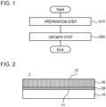
- the flow chart of Fig. 1 shows an example of the processing flow of the method for manufacturing a group III nitride semiconductor substrate of the present embodiment. As illustrated, the method for manufacturing a group III nitride semiconductor substrate of the present embodiment has a preparation step S10 and a growth step S20.
- the group III nitride semiconductor substrate (template substrate) in which a sapphire substrate having a semipolar plane as a main surface, and a group III nitride semiconductor layer positioned over the main surface are laminated is prepared.
- the group III nitride semiconductor substrate has the characteristic that a ⁇ 0002> direction of a sapphire substrate and a ⁇ 10-10> direction of the group III nitride semiconductor layer do not intersect at right angles in a plan view in a direction perpendicular to the main surface of the sapphire substrate.
- the semipolar plane is a plane different from a polar plane (c-plane) and non-polar planes (a-plane and m-plane).
- template group III nitride semiconductor substrate referred to below as “template group III nitride semiconductor substrate"
- Fig. 2 shows a schematic side surface view of an example of the template group III nitride semiconductor substrate 1.
- the template group III nitride semiconductor substrate 1 has a sapphire substrate 10, a buffer layer 20, and a group III nitride semiconductor layer 30.
- the template group III nitride semiconductor substrate 1 may include other layers in addition to the sapphire substrate 10 and the group III nitride semiconductor layer 30.
- the sapphire substrate 10, a buffer layer 20, and the group III nitride semiconductor layer 30 are laminated in this order.
- a layer other than the buffer layer 20 may be interposed between the sapphire substrate 10 and the group III nitride semiconductor layer 30.
- the group III nitride semiconductor layer 30 As described in detail below, in the example of the method for manufacturing the template group III nitride semiconductor substrate 1 shown in Fig. 2 , it is possible to include a step of supplying a gas including any of Al, Ti, Cu, and V over a main surface 11 of the sapphire substrate 10, before forming the buffer layer 20 over the sapphire substrate 10.
- a film of the above metals, a metal carbide film of aluminum carbide, titanium carbide, copper carbide, or vanadium carbide, which is a reaction film with a hydrocarbon compound such as methane, ethylene, ethane, or the like generated from an organometallic raw material, or the like may or may not be formed between the sapphire substrate 10 and the buffer layer 20.
- the metal film may be uniformly spread over the entire main surface 11 of the sapphire substrate 10 or may be dotted over the main surface 11.
- the main surface 11 of the sapphire substrate 10 is a semipolar plane, wherein the main surface 11 is a plane obtained by inclining the ⁇ 10-10 ⁇ plane at any angle of more than 0.0° and 10.5° or less in the direction in which the ⁇ 10-10 ⁇ plane is parallel with the a-plane.
- the thickness of the sapphire substrate 10 is, for example, 250 ⁇ m or more.
- the diameter of the sapphire substrate 10 is, for example, 2.54 cm (1 inch) or more.
- the buffer layer 20 is, for example, an AlN layer or a TiN layer.
- the thickness of the buffer layer 20 is, for example, 20 nm or more and 300 nm or less.
- the group III nitride semiconductor layer 30 is positioned over the main surface 11 of the sapphire substrate 10 with the buffer layer 20 interposed therebetween.
- the group III nitride semiconductor layer 30 is formed of a group III nitride semiconductor crystal (for example, GaN crystal).
- the thickness of the group III nitride semiconductor layer 30 is, for example, 1 ⁇ m or more and 20 ⁇ m or less.
- a growth plane 31 (exposed surface) of the group III nitride semiconductor layer 30 is a semipolar plane inclined from a -C-plane at 38.0° or more and 53.0° or less to the -a-plane direction and -16.0° or more and 16.0° or less to the m-plane direction.
- the growth plane 31 is a plane obtained by inclining the ⁇ 11-23 ⁇ plane (for example, (-1-12-3) plane) at any angle of -16.0° or more and 16.0° or less in a direction in which the ⁇ 11-23 ⁇ is parallel with the m-plane.
- Fig. 3 shows a schematic plan view of an example of the template group III nitride semiconductor substrate 1.
- This diagram shows a state in which the template group III nitride semiconductor substrate 1 is observed from the side of the group III nitride semiconductor layer 30 in a plan view in a direction perpendicular to the main surface 11 of the sapphire substrate 10.
- the ⁇ 0002> direction of the sapphire substrate 10 and the ⁇ 10-10> direction of the group III nitride semiconductor layer 30 observed in a plan view are shown.
- the illustrated arrows indicate the directions in which each of the ⁇ 0002> direction of the sapphire substrate 10 and the ⁇ 10-10> direction of the group III nitride semiconductor layer 30 are projected over a plane in parallel with the main surface 11.
- the template group III nitride semiconductor substrate 1 has a characteristic that a ⁇ 0002> direction of the sapphire substrate 10 (a direction in which the ⁇ 0002> direction is projected over a surface in parallel with the main surface 11) and a ⁇ 10-10> direction of the group III nitride semiconductor layer 30 (a direction in which the ⁇ 10-10> direction projected over a surface in parallel with the main surface 11) do not intersect at right angles in a plan view in a direction perpendicular to the main surface 11.
- the angle formed by the ⁇ 0002> direction of the sapphire substrate 10 and the ⁇ 10-10> direction of the group III nitride semiconductor layer 30 in a plan view in the direction perpendicular to the main surface 11 is not orthogonal, but, for example, as shown in the following Examples, it is possible to set the angle to 44.5° or more and 45.5° or less.
- a group III nitride semiconductor for example, GaN crystal
- a group III nitride semiconductor for example, GaN crystal
- the method for growing the group III nitride semiconductor in the growth step S20 is a matter of design.
- the method for growing the group III nitride semiconductor it is possible to select, for example, vapor phase epitaxial growth (for example, hydride vapor phase epitaxy (HVPE) , metal organic chemical vapor deposition (MOCVD), molecular beam epitaxy (MBE)), liquid phase epitaxial growth, solid phase epitaxial growth, and the like. It is possible to set these growth conditions according to the related art.
- the growth step S20 it is possible to grow a group III nitride semiconductor as a thick film. It is possible to set the thickness of the group III nitride semiconductor layer 40 to, for example, 50 ⁇ m or more and 1000 ⁇ m or less, preferably 100 ⁇ m or more and 1000 ⁇ m or less, and more preferably 500 ⁇ m or more and 1000 ⁇ m or less.
- the growth plane 41 is similarly a semipolar plane.
- the growth plane 41 is a plane obtained by inclining the ⁇ 11-23 ⁇ plane (for example, (-1-12-3) plane) at any angle of more than 0° to 10.0° or less in a direction in which the ⁇ 11-23 ⁇ plane is parallel with the m-plane.
- the method for manufacturing a group III nitride semiconductor substrate of the present embodiment over the template III group nitride semiconductor substrate 1 in which the sapphire substrate 10 and group III nitride semiconductor layer 30 are laminated and in addition, the buffer layer 20 is laminated, it is possible to manufacture a group III nitride semiconductor substrate (refer to Fig. 4 ) in which the group III nitride semiconductor layer 40 is formed.
- the group III nitride semiconductor layer 40 is formed over the template III group nitride semiconductor substrate 1 in which the relative orientation relationship between the ⁇ 0002> direction of the sapphire substrate 10 and the ⁇ 10-10> direction of the group III nitride semiconductor layer 30 is a characteristic relationship (there is no intersection thereof at right angles in a plan view in a direction perpendicular to the main surface 11).
- the group III nitride semiconductor layer 40 is formed over the template group III nitride semiconductor substrate 1 in which the ⁇ 0002> direction of the sapphire substrate 10 and the ⁇ 10-10> direction of the group III nitride semiconductor layer 30 have the characteristic relationship above, even if the group III nitride semiconductor layer 40 is grown as a thick film of 50 ⁇ m or more and 1000 ⁇ m or less, cracks are not easily generated in the group III nitride semiconductor layer 30 and the group III nitride semiconductor layer 40.
- the present embodiment it is possible to grow a group III nitride semiconductor as a thick film over the exposed surface (the growth plane 31) of the template group III nitride semiconductor substrate 1 in which the sapphire substrate 10 and the group III nitride semiconductor layer 30 having a semipolar plane as the exposed surface (the growth plane 31) are laminated.
- the group III nitride semiconductor substrate obtained by the manufacturing method of the present embodiment for example, as a substrate for forming devices such as optical devices and electronic devices.
- the group III nitride semiconductor substrate obtained by the manufacturing method of the present embodiment for example, it is possible to separate the group III nitride semiconductor layer 40 from the sapphire substrate 10 or the like by any means, and to use the group III nitride semiconductor layer 40 as a free-standing substrate.
- the flow chart of Fig. 5 shows an example of the processing flow of the method for manufacturing a group III nitride semiconductor substrate of the present embodiment.
- the method for manufacturing the template group III nitride semiconductor substrate 1 of the present embodiment has a sapphire substrate preparation step S11, a heating step S12, a pre-step S13, a buffer layer forming step S14, and a group III nitride semiconductor layer forming step S15.
- the preparation step S10 shown in Fig. 1 may include these steps.
- the method for manufacturing the template group III nitride semiconductor substrate 1 described below is merely an example. As long as the template III group nitride semiconductor substrate 1 prepared in preparation step S10 is provided with the conditions described above, the template III group nitride semiconductor substrate 1 is not limited to being obtained by the above manufacturing method.
- the sapphire substrate 10 in which the main surface 11 is a semipolar plane is prepared.
- the sapphire substrate 10 is prepared in which the main surface 11 is a plane obtained by inclining the ⁇ 10-10 ⁇ plane at any angle of more than 0.0° and 10.5° or less in a direction in which the ⁇ 10-10 ⁇ plane is parallel with the a-plane.
- the diameter of the sapphire substrate 10 is, for example, 2.54 cm (1 inch) or more.
- the thickness of the sapphire substrate 10 is, for example, 250 ⁇ m or more.
- the sapphire substrate 10 is heated while performing a nitriding treatment.
- the sapphire substrate 10 is heated under the following conditions.
- a gas (pre-treatment gas) including any of Al, Ti, Cu, and V is supplied over the sapphire substrate 10 and NH 3 is not supplied.
- the pre-treatment gas is, for example, trimethylaluminum or the like.
- the gas is supplied under the following conditions.
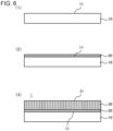
- buffer layer forming step S14 after the pre-treatment step S13 as shown in Fig. 6 (2), the buffer layer 20 is formed over the main surface 11 of the sapphire substrate 10.
- the buffer layer 20 is an AlN layer
- an AlN crystal is epitaxially grown under the following conditions to form the buffer layer 20.
- the buffer layer 20 with a film thickness of 20 nm or more and 300 nm or less is formed.
- the group III nitride semiconductor layer 30 is formed over the buffer layer 20.
- a group III nitride semiconductor crystal for example, GaN
- the group III nitride semiconductor layer 30 having a thickness of 10 ⁇ m or more and 15 ⁇ m or less is formed.
- the template group III nitride semiconductor substrate 1 of the present embodiment having the characteristics described above is obtained.
- the template group III nitride semiconductor substrate 1 it is possible to grow a group III nitride semiconductor (the group III nitride semiconductor layer 40) as a thick film over an exposed surface (growth plane 31) of the substrate (template group III nitride semiconductor substrate 1) in which the sapphire substrate 10 and the group III nitride semiconductor layer 30 having a semipolar plane as the exposed surface (the growth plane 31) are laminated.
- Template group III nitride semiconductor substrates corresponding to each of Example 1, Comparative Example 1, and Comparative Example 2 were prepared.
- a group III nitride semiconductor substrate was manufactured as follows.
- sapphire substrate was prepared (sapphire substrate preparation step S11).
- the prepared sapphire substrate was heated under the following conditions (heating step S12).
- the pre-step S13 was performed on the sapphire substrate after the heating step S12 under the following conditions.
- an AlN layer (buffer layer) having a film thickness of 150 nm was formed over the main surface (exposed surface) of the sapphire substrate under the following conditions.
- GaN layer (a group III nitride semiconductor layer) with a thickness of 15 ⁇ m was formed over the buffer layer 20 under the following conditions.
- the template group III nitride semiconductor substrate of Example 1 was manufactured.
- Fig. 7 is a view showing the relationship (polarity coordinates measurement results) between a ⁇ 0002> direction of a sapphire substrate and a ⁇ 10-10> direction of the group III nitride semiconductor layer (GaN) in a plan view in a direction perpendicular to the main surface of the sapphire substrate.
- the relationship is "non-intersecting at right angles". The angle formed by the above was 44.5° or more and 45.5° or less.
- a template group III nitride semiconductor substrate was manufactured with the buffer layer forming step S14 and the group III nitride semiconductor layer forming step S15 set to the following growth conditions.
- the heating step S12 and the pre-step S13 were the same as in Example 1.
- Fig. 8 shows the relationship (polarity coordinates measurement results) between a ⁇ 0002> direction of a sapphire substrate and a ⁇ 10-10> direction of the group III nitride semiconductor layer (GaN) in a plan view in a direction perpendicular to the main surface of the sapphire substrate. As illustrated, in Comparative Example 1, the relationship is "intersecting with each other at right angles".
- a template group III nitride semiconductor substrate was manufactured with the same manufacturing method as Comparative Example 1.
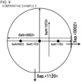
- Fig. 9 shows the relationship (polarity coordinates measurement results) between a ⁇ 0002> direction of a sapphire substrate and a ⁇ 10-10> direction of the group III nitride semiconductor layer (GaN) in a plan view in a direction perpendicular to the main surface of the sapphire substrate. As illustrated, in Comparative Example 2, the relationship is "intersecting each other at right angles".
- a GaN layer having a film thickness of 200 ⁇ m was formed under the following conditions.
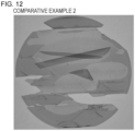
- Fig. 10 to Fig. 12 show the appearance of group III nitride semiconductor substrates in which a GaN layer was grown as a thick film over a template group III nitride semiconductor substrate.
- Fig. 10 shows the group III nitride semiconductor substrate of Example 1
- Fig. 11 shows Comparative Example 1
- Fig. 12 shows Comparative Example 2.
- Example 1 it is understood that it is possible to manufacture a template group III nitride semiconductor substrate having a sapphire substrate having a semipolar plane as a main surface, and a group III nitride semiconductor layer positioned over the main surface, in which a ⁇ 0002> direction of the sapphire substrate and a ⁇ 10-10> direction of the group III nitride semiconductor layer do not intersect at right angles in a plan view in a direction perpendicular to the main surface.
Landscapes
- Chemical & Material Sciences (AREA)
- Engineering & Computer Science (AREA)
- Materials Engineering (AREA)
- Metallurgy (AREA)
- Organic Chemistry (AREA)
- General Chemical & Material Sciences (AREA)
- Chemical Kinetics & Catalysis (AREA)
- Crystallography & Structural Chemistry (AREA)
- Inorganic Chemistry (AREA)
- Mechanical Engineering (AREA)
- Chemical Vapour Deposition (AREA)
- Crystals, And After-Treatments Of Crystals (AREA)
Description
- The present invention relates to a group III nitride semiconductor substrate and a method for manufacturing a group III nitride semiconductor substrate.
- Related techniques are disclosed in
Patent Document 1,Patent Document 2, andPatent Document 3. As disclosed inPatent Document 1 andPatent Document 2, in a case where a device (for example, an optical device, an electronic device, or the like) is formed over the c-plane of a group III nitride semiconductor crystal, the internal quantum efficiency is reduced due to a piezoelectric field. Therefore, attempts are being made to form devices over so-called semipolar planes (planes different from polar planes and non-polar planes).Patent Document 3 discloses a group III nitride semiconductor substrate comprising a sapphire substrate and a group III nitride semiconductor layer positioned over the main surface of the sapphire substrate, wherein, inter alia, the projected [01-10] axis of GaN and the projected [0001] axis of the sapphire substrate are perpendicular to each other in the plan view of the main surface of the sapphire substrate. -
- [Patent Document 1]
Japanese Patent Application Publication No. 2012-160755 - [Patent Document 2]
Japanese Patent Application Publication No. 2016-12717 - [Patent Document 3]
European Patent Application Publication No. 1 182 697 A2 - The present inventors have newly discovered that, in a case where a group III nitride semiconductor is grown as a thick film over a substrate, in which a sapphire substrate and a group III nitride semiconductor layer having a semipolar plane as an exposed surface are laminated, over the exposed surface thereof, cracks may occur in the group III nitride semiconductor layer, which may cause the semiconductor substrate layer to be peeled off from the sapphire substrate. In some cases, cracks may also occur on the sapphire substrate side.
- The present invention has an object of providing a new technique for growing a group III nitride semiconductor as a thick film over a substrate, in which a sapphire substrate and a group III nitride semiconductor layer having a semipolar plane as an exposed surface are laminated, over the exposed surface thereof.
- According to a first aspect of the present invention, there is provided a group III nitride semiconductor substrate comprising a sapphire substrate having a semipolar plane as a main surface, a group III nitride semiconductor layer positioned over the main surface, and a buffer layer interposed between the sapphire substrate and the group III nitride semiconductor layer, wherein a <0002> direction of the sapphire substrate and a <10-10> direction of the group III nitride semiconductor layer do not intersect at right angles in a plan view in a direction perpendicular to the main surface, wherein the main surface is a plane obtained by inclining a {10-10} plane at any angle of more than 0.0° and 10.5° or less in a direction in which the {10-10} plane is parallel with an a-plane, and the group III nitride semiconductor layer has a semipolar plane inclined from a -C-plane at 38.0° or more and 53.0° or less to a -a-plane direction and at -16.0° or more and 16.0° or less to a m-plane direction as an exposed surface.
- In addition, according to a second aspect of the present invention, there is provided a method for manufacturing a group III nitride semiconductor substrate, the method comprising: a preparation step of preparing a group III nitride semiconductor substrate having a sapphire substrate having a semipolar plane as a main surface, and a group III nitride semiconductor layer positioned over the main surface, in which a <0002> direction of the sapphire substrate and a <10-10> direction of the group III nitride semiconductor layer do not intersect at right angles in a plan view in a direction perpendicular to the main surface, and a growth step of epitaxially growing a group III nitride semiconductor over the group III nitride semiconductor layer, wherein the preparation step comprises:
- a sapphire substrate preparation step of preparing a sapphire substrate in which the main surface is a plane obtained by inclining a {10-10} plane at any angle of more than 0.0° and 10.5° or less in a direction in which the {10-10} plane is parallel with an a-plane;
- a heating step of heating the sapphire substrate while performing a nitriding treatment;
- a pre-step of supplying a gas including any of Al, Ti, Cu, and V without supplying NH3 over the sapphire substrate after the heating step;
- a buffer layer forming step of forming a buffer layer over the main surface after the pre-step, wherein, in the buffer layer forming step, the buffer layer is formed at a growth temperature of 800°C or higher and 950°C or lower; and
- a group III nitride semiconductor layer forming step of forming a group III nitride semiconductor layer over the buffer layer.
- Preferred embodiments of the first and second aspects of the invention are set forth in
claims 2 and 4. - The present invention realizes a new technique for growing a group III nitride semiconductor as a thick film over a substrate, in which a sapphire substrate and a group III nitride semiconductor layer having a semipolar plane as an exposed surface are laminated, over the exposed surface thereof.
- The objects described above, other objects, characteristics, and advantages will become clearer from the preferred embodiments described below and the following associated drawings.
-
Fig. 1 is a flow chart showing an example of a processing flow of a method for manufacturing a group III nitride semiconductor substrate of the present embodiment. -
Fig. 2 is a schematic side surface view of an example of a template group IIInitride semiconductor substrate 1 of the present embodiment. -
Fig. 3 is a schematic plan view of an example of the template group IIInitride semiconductor substrate 1 of the present embodiment. -
Fig. 4 is a schematic side surface view of an example of the group III nitride semiconductor substrate of the present embodiment obtained by forming a group IIInitride semiconductor layer 40 over the template group IIInitride semiconductor substrate 1 of the present embodiment. -
Fig. 5 is a flow chart showing an example of a processing flow of a method for manufacturing the template group IIInitride semiconductor substrate 1 of the present embodiment. -
Fig. 6 is a step diagram showing an example of a processing flow of a method for manufacturing the template group IIInitride semiconductor substrate 1 of the present embodiment. -
Fig. 7 is a view showing a relationship in a group III nitride semiconductor substrate of Example 1 between a <0002> direction of a sapphire substrate and a <10-10> direction of a group III nitride semiconductor layer in a plan view in a direction perpendicular to the main surface of the sapphire substrate. -
Fig. 8 is a view showing the relationship in a group III nitride semiconductor substrate of Comparative Example 1 between a <0002> direction of a sapphire substrate and a <10-10> direction of a group III nitride semiconductor layer in a plan view in a direction perpendicular to the main surface of the sapphire substrate. -
Fig. 9 is a view showing the relationship in a group III nitride semiconductor substrate of Comparative Example 2 between a <0002> direction of a sapphire substrate and a <10-10> direction of a group III nitride semiconductor layer in a plan view in a direction perpendicular to the main surface of the sapphire substrate. -
Fig. 10 is a view showing a state after a group III nitride semiconductor layer is grown as a thick film over the group III nitride semiconductor substrate of Example 1. -
Fig. 11 is a view showing a state after a group III nitride semiconductor layer is grown as a thick film over the group III nitride semiconductor substrate of Comparative Example 1. -
Fig. 12 is a view showing a state after a group III nitride semiconductor layer is grown as a thick film over the group III nitride semiconductor substrate of Comparative Example 2. - A description will be given below of embodiments of a group III nitride semiconductor substrate and a method for manufacturing a group III nitride semiconductor substrate of the present invention using the drawings. The drawings are merely schematic views for illustrating the configuration of the invention, and the size, shape, and number of each member, the ratios of sizes of different members, and the like are not limited to the illustrated examples.
- The flow chart of
Fig. 1 shows an example of the processing flow of the method for manufacturing a group III nitride semiconductor substrate of the present embodiment. As illustrated, the method for manufacturing a group III nitride semiconductor substrate of the present embodiment has a preparation step S10 and a growth step S20. - In the preparation step S10, the group III nitride semiconductor substrate (template substrate) in which a sapphire substrate having a semipolar plane as a main surface, and a group III nitride semiconductor layer positioned over the main surface are laminated is prepared. The group III nitride semiconductor substrate has the characteristic that a <0002> direction of a sapphire substrate and a <10-10> direction of the group III nitride semiconductor layer do not intersect at right angles in a plan view in a direction perpendicular to the main surface of the sapphire substrate. The semipolar plane is a plane different from a polar plane (c-plane) and non-polar planes (a-plane and m-plane).
- A detailed description will be given of a group III nitride semiconductor substrate (referred to below as "template group III nitride semiconductor substrate") to be prepared in preparation step S10.
-
Fig. 2 shows a schematic side surface view of an example of the template group IIInitride semiconductor substrate 1. As shown inFig. 2 , the template group IIInitride semiconductor substrate 1 has asapphire substrate 10, abuffer layer 20, and a group IIInitride semiconductor layer 30. The template group IIInitride semiconductor substrate 1 may include other layers in addition to thesapphire substrate 10 and the group IIInitride semiconductor layer 30. In the illustrated example, thesapphire substrate 10, abuffer layer 20, and the group IIInitride semiconductor layer 30 are laminated in this order. - A layer other than the
buffer layer 20 may be interposed between thesapphire substrate 10 and the group IIInitride semiconductor layer 30. As described in detail below, in the example of the method for manufacturing the template group IIInitride semiconductor substrate 1 shown inFig. 2 , it is possible to include a step of supplying a gas including any of Al, Ti, Cu, and V over amain surface 11 of thesapphire substrate 10, before forming thebuffer layer 20 over thesapphire substrate 10. As a result of this step, a film of the above metals, a metal carbide film of aluminum carbide, titanium carbide, copper carbide, or vanadium carbide, which is a reaction film with a hydrocarbon compound such as methane, ethylene, ethane, or the like generated from an organometallic raw material, or the like may or may not be formed between thesapphire substrate 10 and thebuffer layer 20. In a case where the metal film is formed, the metal film may be uniformly spread over the entiremain surface 11 of thesapphire substrate 10 or may be dotted over themain surface 11. - The
main surface 11 of thesapphire substrate 10 is a semipolar plane, wherein themain surface 11 is a plane obtained by inclining the {10-10} plane at any angle of more than 0.0° and 10.5° or less in the direction in which the {10-10} plane is parallel with the a-plane. The thickness of thesapphire substrate 10 is, for example, 250 µm or more. In addition, the diameter of thesapphire substrate 10 is, for example, 2.54 cm (1 inch) or more. - The
buffer layer 20 is, for example, an AlN layer or a TiN layer. The thickness of thebuffer layer 20 is, for example, 20 nm or more and 300 nm or less. - The group III
nitride semiconductor layer 30 is positioned over themain surface 11 of thesapphire substrate 10 with thebuffer layer 20 interposed therebetween. The group IIInitride semiconductor layer 30 is formed of a group III nitride semiconductor crystal (for example, GaN crystal). The thickness of the group IIInitride semiconductor layer 30 is, for example, 1 µm or more and 20 µm or less. - A growth plane 31 (exposed surface) of the group III
nitride semiconductor layer 30 is a semipolar plane inclined from a -C-plane at 38.0° or more and 53.0° or less to the -a-plane direction and -16.0° or more and 16.0° or less to the m-plane direction. For example, thegrowth plane 31 is a plane obtained by inclining the {11-23} plane (for example, (-1-12-3) plane) at any angle of -16.0° or more and 16.0° or less in a direction in which the {11-23} is parallel with the m-plane. -
Fig. 3 shows a schematic plan view of an example of the template group IIInitride semiconductor substrate 1. This diagram shows a state in which the template group IIInitride semiconductor substrate 1 is observed from the side of the group IIInitride semiconductor layer 30 in a plan view in a direction perpendicular to themain surface 11 of thesapphire substrate 10. In the diagram, the <0002> direction of thesapphire substrate 10 and the <10-10> direction of the group IIInitride semiconductor layer 30 observed in a plan view are shown. The illustrated arrows indicate the directions in which each of the <0002> direction of thesapphire substrate 10 and the <10-10> direction of the group IIInitride semiconductor layer 30 are projected over a plane in parallel with themain surface 11. - As shown in the diagram, the template group III
nitride semiconductor substrate 1 has a characteristic that a <0002> direction of the sapphire substrate 10 (a direction in which the <0002> direction is projected over a surface in parallel with the main surface 11) and a <10-10> direction of the group III nitride semiconductor layer 30 (a direction in which the <10-10> direction projected over a surface in parallel with the main surface 11) do not intersect at right angles in a plan view in a direction perpendicular to themain surface 11. - It is only necessary that the angle formed by the <0002> direction of the
sapphire substrate 10 and the <10-10> direction of the group IIInitride semiconductor layer 30 in a plan view in the direction perpendicular to themain surface 11 is not orthogonal, but, for example, as shown in the following Examples, it is possible to set the angle to 44.5° or more and 45.5° or less. - Returning to
Fig. 1 , in the growth step S20, a group III nitride semiconductor (for example, GaN crystal) is epitaxially grown over thegrowth plane 31 of the group IIInitride semiconductor layer 30. As a result, as shown inFig. 4 , it is possible to obtain a group III nitride semiconductor substrate in which the group IIInitride semiconductor layer 40 is formed over the group IIInitride semiconductor layer 30 of the template III groupnitride semiconductor substrate 1. - The method for growing the group III nitride semiconductor in the growth step S20 is a matter of design. As the method for growing the group III nitride semiconductor, it is possible to select, for example, vapor phase epitaxial growth (for example, hydride vapor phase epitaxy (HVPE) , metal organic chemical vapor deposition (MOCVD), molecular beam epitaxy (MBE)), liquid phase epitaxial growth, solid phase epitaxial growth, and the like. It is possible to set these growth conditions according to the related art.
- As shown in the following examples, even if the group III nitride semiconductor is grown as a thick film over the template III group
nitride semiconductor substrate 1 of the present embodiment, problems such as cracking and peeling are not easily generated. For this reason, in the growth step S20, it is possible to grow a group III nitride semiconductor as a thick film. It is possible to set the thickness of the group IIInitride semiconductor layer 40 to, for example, 50 µm or more and 1000 µm or less, preferably 100 µm or more and 1000 µm or less, and more preferably 500 µm or more and 1000 µm or less. - In the group III
nitride semiconductor layer 40 obtained by epitaxial growth over thegrowth plane 31 of the group IIInitride semiconductor layer 30, thegrowth plane 41 is similarly a semipolar plane. For example, thegrowth plane 41 is a plane obtained by inclining the {11-23} plane (for example, (-1-12-3) plane) at any angle of more than 0° to 10.0° or less in a direction in which the {11-23} plane is parallel with the m-plane. - As described above, according to the method for manufacturing a group III nitride semiconductor substrate of the present embodiment, over the template III group
nitride semiconductor substrate 1 in which thesapphire substrate 10 and group IIInitride semiconductor layer 30 are laminated and in addition, thebuffer layer 20 is laminated, it is possible to manufacture a group III nitride semiconductor substrate (refer toFig. 4 ) in which the group IIInitride semiconductor layer 40 is formed. - In addition, in the manufacturing method of the present embodiment, the group III
nitride semiconductor layer 40 is formed over the template III groupnitride semiconductor substrate 1 in which the relative orientation relationship between the <0002> direction of thesapphire substrate 10 and the <10-10> direction of the group IIInitride semiconductor layer 30 is a characteristic relationship (there is no intersection thereof at right angles in a plan view in a direction perpendicular to the main surface 11). - As shown in the following Examples, in a case where the <0002> direction of the
sapphire substrate 10 and the <10-10> direction of the group IIInitride semiconductor layer 30 intersect at right angles each other in a plan view in the direction perpendicular to themain surface 11, when the group IIInitride semiconductor layer 40 is grown as a thick film of 50 µm or more, the group IIInitride semiconductor layer 30 and the group IIInitride semiconductor layer 40 are easily cracked. Then, due to these cracks, the group IIInitride semiconductor layer 30 and the group IIInitride semiconductor layer 40 are separated, and a problem of unintentional peeling from thesapphire substrate 10 is easily generated. - In the case of the present embodiment in which the group III
nitride semiconductor layer 40 is formed over the template group IIInitride semiconductor substrate 1 in which the <0002> direction of thesapphire substrate 10 and the <10-10> direction of the group IIInitride semiconductor layer 30 have the characteristic relationship above, even if the group IIInitride semiconductor layer 40 is grown as a thick film of 50 µm or more and 1000 µm or less, cracks are not easily generated in the group IIInitride semiconductor layer 30 and the group IIInitride semiconductor layer 40. - That is, according to the present embodiment, it is possible to grow a group III nitride semiconductor as a thick film over the exposed surface (the growth plane 31) of the template group III
nitride semiconductor substrate 1 in which thesapphire substrate 10 and the group IIInitride semiconductor layer 30 having a semipolar plane as the exposed surface (the growth plane 31) are laminated. - It is possible to use the group III nitride semiconductor substrate obtained by the manufacturing method of the present embodiment, for example, as a substrate for forming devices such as optical devices and electronic devices. In addition, in the group III nitride semiconductor substrate obtained by the manufacturing method of the present embodiment, for example, it is possible to separate the group III
nitride semiconductor layer 40 from thesapphire substrate 10 or the like by any means, and to use the group IIInitride semiconductor layer 40 as a free-standing substrate. - Next, a description will be given of an example of a method for manufacturing the template group III
nitride semiconductor substrate 1 of the present embodiment. The flow chart ofFig. 5 shows an example of the processing flow of the method for manufacturing a group III nitride semiconductor substrate of the present embodiment. As illustrated, the method for manufacturing the template group IIInitride semiconductor substrate 1 of the present embodiment has a sapphire substrate preparation step S11, a heating step S12, a pre-step S13, a buffer layer forming step S14, and a group III nitride semiconductor layer forming step S15. For example, the preparation step S10 shown inFig. 1 may include these steps. - The method for manufacturing the template group III
nitride semiconductor substrate 1 described below is merely an example. As long as the template III groupnitride semiconductor substrate 1 prepared in preparation step S10 is provided with the conditions described above, the template III groupnitride semiconductor substrate 1 is not limited to being obtained by the above manufacturing method. - In the sapphire substrate preparation step S11, as shown in
Fig. 6 (1), thesapphire substrate 10 in which themain surface 11 is a semipolar plane is prepared. In the sapphire substrate preparation step S11, thesapphire substrate 10 is prepared in which themain surface 11 is a plane obtained by inclining the {10-10} plane at any angle of more than 0.0° and 10.5° or less in a direction in which the {10-10} plane is parallel with the a-plane. - The diameter of the
sapphire substrate 10 is, for example, 2.54 cm (1 inch) or more. In addition, the thickness of thesapphire substrate 10 is, for example, 250 µm or more. - In the heating step S12, the
sapphire substrate 10 is heated while performing a nitriding treatment. For example, thesapphire substrate 10 is heated under the following conditions. - Temperature: 800°C or higher and 1200°C or lower
- Pressure: 67 hPa (50 torr) or more and 333 hPa (250 torr) or less
- Heat treatment time: 15 minutes
- Carrier gas: H2, N2
- H2 (carrier gas) supply rate: 8.5 slm or more and 9.5 slm or less
- N2 (carrier gas) supply rate: 1.0 slm or more and 2.0 slm or less
- NH3 supply rate: 15 slm or more and 20 slm or less
- In the pre-step S13, after the heating step S12, a gas (pre-treatment gas) including any of Al, Ti, Cu, and V is supplied over the
sapphire substrate 10 and NH3 is not supplied. The pre-treatment gas is, for example, trimethylaluminum or the like. For example, the gas is supplied under the following conditions. - Temperature: 500°C or higher and 1000°C or lower
- Pressure: 40 hPa (30 torr) or more and 267 hPa (200 torr) or less
- Treatment time: 10 seconds
- Carrier gas: H2, N2
- H2 (carrier gas) supply rate: 8.5 slm or more and 9.5 slm or less
- N2 (carrier gas) supply rate: 1.0 slm or more and 2.0 slm or less
- NH3 supply rate: 0 slm
- Pre-treatment gas (example: trimethyl aluminum) supply rate: 85 ccm or more and 95 ccm or less
- In buffer layer forming step S14, after the pre-treatment step S13 as shown in
Fig. 6 (2), thebuffer layer 20 is formed over themain surface 11 of thesapphire substrate 10. In a case where thebuffer layer 20 is an AlN layer, for example, an AlN crystal is epitaxially grown under the following conditions to form thebuffer layer 20. As a result, thebuffer layer 20 with a film thickness of 20 nm or more and 300 nm or less is formed. - Growth method: MOCVD method
- Growth temperature: 800°C or higher and 950°C or lower
- Pressure: 40 hPa (30 torr) or more and 267 hPa (200 torr) or less
- V/III ratio: 4000 or more and 6000 or less
- TMAl supply rate: 20 ccm or more and 500 ccm or less
- NH3 supply rate: 2.5 slm or more and 7.5 slm or less
- Carrier gas: H2, N2
- H2 (carrier gas) supply rate: 8.5 slm or more and 9.5 slm or less
- N2 (carrier gas) supply rate: 1.0 slm or more and 2.0 slm or less
- In the group III nitride semiconductor layer forming step S15, as shown in
Fig. 6 (3), the group IIInitride semiconductor layer 30 is formed over thebuffer layer 20. For example, a group III nitride semiconductor crystal (for example, GaN) is epitaxially grown under the following growth conditions to form the group IIInitride semiconductor layer 30. As a result, the group IIInitride semiconductor layer 30 having a thickness of 10 µm or more and 15 µm or less is formed. - Growth method: MOCVD method
- Growth temperature: 800°C or higher to 1025°C or lower
- Pressure: 40 hPa (30 torr) or more and 267 hPa (200 torr) or less
- V/III ratio: 200 or more and 500 or less
- TMGa supply rate: 50 ccm or more and 1000 ccm or less
- NH3 supply rate: 9.0 slm or more and 11.0 slm or less
- Carrier gas: H2, N2
- H2 (carrier gas) supply rate: 13.0 slm or more and 14.0 slm or less
- N2 (carrier gas) supply rate: 1.0 slm or more and 2.0 slm or less
- Thus, the template group III
nitride semiconductor substrate 1 of the present embodiment having the characteristics described above is obtained. By using the template group IIInitride semiconductor substrate 1, it is possible to grow a group III nitride semiconductor (the group III nitride semiconductor layer 40) as a thick film over an exposed surface (growth plane 31) of the substrate (template group III nitride semiconductor substrate 1) in which thesapphire substrate 10 and the group IIInitride semiconductor layer 30 having a semipolar plane as the exposed surface (the growth plane 31) are laminated. - Template group III nitride semiconductor substrates corresponding to each of Example 1, Comparative Example 1, and Comparative Example 2 were prepared.
- A template group III nitride semiconductor substrate having a sapphire substrate having a semipolar plane as a main surface, and a group III nitride semiconductor layer positioned over the main surface, in which a <0002> direction of the sapphire substrate and a <10-10> direction of the group III nitride semiconductor layer "do not intersect at right angles" in a plan view in a direction perpendicular to the main surface, was prepared. Specifically, a group III nitride semiconductor substrate was manufactured as follows.
- First, the following sapphire substrate was prepared (sapphire substrate preparation step S11).
- Main surface (exposed surface): A plane obtained by inclining the (10-10) plane at 2.0° in the direction in which the (10-10) plane is parallel with the a-plane
- Thickness: 430 µm
- Diameter: 5.08 cm (2 inches)
- The prepared sapphire substrate was heated under the following conditions (heating step S12).
- Temperature: 1000°C to 1050°C
- Pressure: 267 hPa (200 torr)
- Heat treatment time: 15 minutes
- Carrier gas: H2, N2
- H2 (carrier gas) supply rate: 9 slm
- N2 (carrier gas) supply rate: 1.5 slm
- NH3 supply rate: 20 slm
- The pre-step S13 was performed on the sapphire substrate after the heating step S12 under the following conditions.
- Temperature: 900 to 930°C
- Pressure: 133 hPa (100 torr)
- Treatment time: 10 seconds
- Carrier gas: H2, N2
- H2 (carrier gas) supply rate: 9 slm
- N2 (carrier gas) supply rate: 1.5 slm
- NH3 supply rate: 0 slm
- Pre-treatment gas (trimethylaluminum) supply rate: 90 sccm
- After the heat treatment, an AlN layer (buffer layer) having a film thickness of 150 nm was formed over the main surface (exposed surface) of the sapphire substrate under the following conditions.
- Growth method: MOCVD method
- Growth temperature: 900 to 930°C
- Pressure: 133 hPa (100 torr)
- V/III ratio: 5184
- TMAl supply rate: 90 ccm
- NH3 supply rate: 5 slm
- Carrier gas: H2, N2
- H2 (carrier gas) supply rate: 9 slm
- N2 (carrier gas) supply rate: 1.5 slm
- Thereafter, a GaN layer (a group III nitride semiconductor layer) with a thickness of 15 µm was formed over the
buffer layer 20 under the following conditions. - Growth method: MOCVD method
- Growth temperature: 900 to 1020° C (continuous change)
- Pressure: 133 hPa (100 torr)
- V/III ratio: 321
- TMGa supply rate: 50 to 500 sccm (continuous change)
- NH3 supply rate: 5 to 10 slm (continuous change)
- Carrier gas: H2, N2
- H2 (carrier gas) supply rate: 13.5 slm
- N2 (carrier gas) supply rate: 1.5 slm
- As described above, the template group III nitride semiconductor substrate of Example 1 was manufactured.
-
Fig. 7 is a view showing the relationship (polarity coordinates measurement results) between a <0002> direction of a sapphire substrate and a <10-10> direction of the group III nitride semiconductor layer (GaN) in a plan view in a direction perpendicular to the main surface of the sapphire substrate. As illustrated, in Example 1, the relationship is "non-intersecting at right angles". The angle formed by the above was 44.5° or more and 45.5° or less. - A template group III nitride semiconductor substrate having a sapphire substrate having a semipolar plane as a main surface, and a group III nitride semiconductor layer positioned over the main surface, in which a <0002> direction of the sapphire substrate and a <10-10> direction of the group III nitride semiconductor layer "intersect at right angles" in a plan view in a direction perpendicular to the main surface, was prepared.
- Specifically, using a sapphire substrate in which the main surface (exposed surface) is a plane obtained by inclining the (10-10) plane at 2.0° in the direction in which the (10-10) plane is parallel with the first surface, a template group III nitride semiconductor substrate was manufactured with the buffer layer forming step S14 and the group III nitride semiconductor layer forming step S15 set to the following growth conditions. The heating step S12 and the pre-step S13 were the same as in Example 1.
- Buffer layer forming step S14
- Growth method: MOCVD method
- Growth temperature: 1050 to 1075°C
- Pressure: 133 hPa (100 torr)
- V/III ratio: 5184
- TMAl supply rate: 90 ccm
- NH3 supply rate: 5 slm
- Carrier gas: H2, N2
- H2 (carrier gas) supply rate: 9 slm
- N2 (carrier gas) supply rate: 1.5 slm
- Group III nitride semiconductor layer forming step S15
- Growth method: MOCVD method
- Growth temperature: 1075 to 1100°C (continuous change)
- Pressure: 13h3 hPa (100 torr)
- V/III ratio: 321
- TMGa supply rate: 50 to 500 sccm (continuous change)
- NH3 supply rate: 5 to 10 slm (continuous change)
- Carrier gas: H2, N2
- H2 (carrier gas) supply rate: 13.5 slm
- N2 (carrier gas) supply rate: 1.5 slm
-
Fig. 8 shows the relationship (polarity coordinates measurement results) between a <0002> direction of a sapphire substrate and a <10-10> direction of the group III nitride semiconductor layer (GaN) in a plan view in a direction perpendicular to the main surface of the sapphire substrate. As illustrated, in Comparative Example 1, the relationship is "intersecting with each other at right angles". - A template group III nitride semiconductor substrate having a sapphire substrate having a semipolar plane as a main surface, and a group III nitride semiconductor layer positioned over the main surface, in which a <0002> direction of the sapphire substrate and a <10-10> direction of the group III nitride semiconductor layer "intersect at right angles" in a plan view in a direction perpendicular to the main surface, was prepared.
- Specifically, using a sapphire substrate having a main surface (exposed surface) obtained by inclining the (10-10) plane at 5.0° in the direction in which the (10-10) plane is parallel with the a-plane, a template group III nitride semiconductor substrate was manufactured with the same manufacturing method as Comparative Example 1.
-
Fig. 9 shows the relationship (polarity coordinates measurement results) between a <0002> direction of a sapphire substrate and a <10-10> direction of the group III nitride semiconductor layer (GaN) in a plan view in a direction perpendicular to the main surface of the sapphire substrate. As illustrated, in Comparative Example 2, the relationship is "intersecting each other at right angles". - Over each of the template group III nitride semiconductor substrates of Example 1 and Comparative Example 1 and Comparative Example 2 prepared in (1), a GaN layer having a film thickness of 200 µm was formed under the following conditions.
- Growth method: HVPE method
- Growth temperature: 1040° C
- Pressure: 985 hPa
- V/III ratio: 10
- GaCl supply rate: 200 sccm
- NH3 supply rate: 2 slm
- Carrier gas: H2
- H2 (carrier gas) supply rate: 8 slm
-
Fig. 10 to Fig. 12 show the appearance of group III nitride semiconductor substrates in which a GaN layer was grown as a thick film over a template group III nitride semiconductor substrate.Fig. 10 shows the group III nitride semiconductor substrate of Example 1,Fig. 11 shows Comparative Example 1, andFig. 12 shows Comparative Example 2. - From
Fig. 10 to Fig. 12 , no cracks are generated in the group III nitride semiconductor substrate in Example 1. On the other hand, in Comparative Example 1 and Comparative Example 2, it was confirmed that cracks were generated in the group III nitride semiconductor layer, which caused parts to peel off from the sapphire substrate. Cracks were generated in the group III nitride semiconductor layer starting from the m-plane which is the cleavage plane of GaN. - In addition, in Comparative Example 1 and Comparative Example 2, cracks were also generated in parts of the sapphire substrate.
- From the above results, between a case where a group III nitride semiconductor is grown as a thick film over a template group III nitride semiconductor substrate having a sapphire substrate having a semipolar plane as a main surface, and a group III nitride semiconductor layer positioned over the main surface, in which a <0002> direction of the sapphire substrate and a <10-10> direction of the group III nitride semiconductor layer do not intersect at right angles in a plan view in a direction perpendicular to the main surface, and a case where a group III nitride semiconductor is grown as a thick film over a template group III nitride semiconductor substrate in which the above intersect at right angles, it is understood that problems such as cracks or peeling are less likely to occur when growing a group III nitride semiconductor as a thick film over a template group III nitride semiconductor substrate in which the above do not intersect at right angles.
- In addition, according to the manufacturing method of Example 1, it is understood that it is possible to manufacture a template group III nitride semiconductor substrate having a sapphire substrate having a semipolar plane as a main surface, and a group III nitride semiconductor layer positioned over the main surface, in which a <0002> direction of the sapphire substrate and a <10-10> direction of the group III nitride semiconductor layer do not intersect at right angles in a plan view in a direction perpendicular to the main surface.
Claims (4)
- A group III nitride semiconductor substrate comprising:a sapphire substrate having a semipolar plane as a main surface;a group III nitride semiconductor layer positioned over the main surface; anda buffer layer interposed between the sapphire substrate and the group III nitride semiconductor layer,wherein a <0002> direction of the sapphire substrate and a <10-10> direction of the group III nitride semiconductor layer do not intersect at right angles in a plan view in a direction perpendicular to the main surface,wherein the main surface is a plane obtained by inclining a {10-10} plane at any angle of more than 0.0° and 10.5° or less in a direction in which the {10-10} plane is parallel with an a-plane, andthe group III nitride semiconductor layer has a semipolar plane inclined from a -C-plane at 38.0° or more and 53.0° or less to a -a-plane direction and at -16.0° or more and 16.0° or less to a m-plane direction as an exposed surface.
- The group III nitride semiconductor substrate according to claim 1, further comprising:
a group III nitride semiconductor layer with a film thickness of 50 µm or more and 1000 µm or less over the group III nitride semiconductor layer. - A method for manufacturing a group III nitride semiconductor substrate, the method comprising:a preparation step of preparing a group III nitride semiconductor substrate having a sapphire substrate having a semipolar plane as a main surface, and a group III nitride semiconductor layer positioned over the main surface, in which a <0002> direction of the sapphire substrate and a <10-10> direction of the group III nitride semiconductor layer do not intersect at right angles in a plan view in a direction perpendicular to the main surface; anda growth step of epitaxially growing a group III nitride semiconductor over the group III nitride semiconductor layer,wherein the preparation step comprises:a sapphire substrate preparation step of preparing a sapphire substrate in which the main surface is a plane obtained by inclining a {10-10} plane at any angle of more than 0.0° and 10.5° or less in a direction in which the {10-10} plane is parallel with an a-plane;a heating step of heating the sapphire substrate while performing a nitriding treatment;a pre-step of supplying a gas including any of Al, Ti, Cu, and V without supplying NH3 over the sapphire substrate after the heating step;a buffer layer forming step of forming a buffer layer over the main surface after the pre-step, wherein, in the buffer layer forming step, the buffer layer is formed at a growth temperature of 800°C or higher and 950°C or lower; anda group III nitride semiconductor layer forming step of forming a group III nitride semiconductor layer over the buffer layer.
- The method for manufacturing a group III nitride semiconductor substrate according to claim 3,
wherein, in the growth step, a group III nitride semiconductor layer with a film thickness of 50 µm or more and 1000 µm or less is formed over the group III nitride semiconductor layer.
Applications Claiming Priority (2)
| Application Number | Priority Date | Filing Date | Title |
|---|---|---|---|
| JP2016245357A JP6306677B1 (en) | 2016-12-19 | 2016-12-19 | Group III nitride semiconductor substrate and method for manufacturing group III nitride semiconductor substrate |
| PCT/JP2017/045392 WO2018117051A1 (en) | 2016-12-19 | 2017-12-18 | Group iii nitride semiconductor substrate and production method for group iii nitride semiconductor substrate |
Publications (3)
| Publication Number | Publication Date |
|---|---|
| EP3556912A1 EP3556912A1 (en) | 2019-10-23 |
| EP3556912A4 EP3556912A4 (en) | 2020-09-09 |
| EP3556912B1 true EP3556912B1 (en) | 2024-03-06 |
Family
ID=61828571
Family Applications (1)
| Application Number | Title | Priority Date | Filing Date |
|---|---|---|---|
| EP17885108.5A Active EP3556912B1 (en) | 2016-12-19 | 2017-12-18 | Group iii nitride semiconductor substrate and production method for group iii nitride semiconductor substrate |
Country Status (8)
| Country | Link |
|---|---|
| US (1) | US10910474B2 (en) |
| EP (1) | EP3556912B1 (en) |
| JP (1) | JP6306677B1 (en) |
| KR (1) | KR102535767B1 (en) |
| CN (1) | CN110088364B (en) |
| PL (1) | PL3556912T3 (en) |
| TW (1) | TWI738944B (en) |
| WO (1) | WO2018117051A1 (en) |
Families Citing this family (1)
| Publication number | Priority date | Publication date | Assignee | Title |
|---|---|---|---|---|
| JP7084784B2 (en) | 2018-05-25 | 2022-06-15 | 株式会社アルファ | Inside handle device |
Family Cites Families (11)
| Publication number | Priority date | Publication date | Assignee | Title |
|---|---|---|---|---|
| US6586819B2 (en) | 2000-08-14 | 2003-07-01 | Nippon Telegraph And Telephone Corporation | Sapphire substrate, semiconductor device, electronic component, and crystal growing method |
| JP2008297138A (en) * | 2007-05-30 | 2008-12-11 | Sumitomo Metal Mining Co Ltd | Group III nitride compound semiconductor manufacturing substrate and manufacturing method thereof |
| JP4935700B2 (en) * | 2008-02-01 | 2012-05-23 | 豊田合成株式会社 | Group III nitride compound semiconductor manufacturing method, wafer, group III nitride compound semiconductor device |
| US8507304B2 (en) * | 2009-07-17 | 2013-08-13 | Applied Materials, Inc. | Method of forming a group III-nitride crystalline film on a patterned substrate by hydride vapor phase epitaxy (HVPE) |
| KR20130035995A (en) * | 2010-02-10 | 2013-04-09 | 다카후미 야오 | Structural body, and method for producing semiconductor substrate |
| WO2012020559A1 (en) | 2010-08-09 | 2012-02-16 | パナソニック株式会社 | Semiconductor light-emitting device |
| JP5573632B2 (en) | 2010-11-25 | 2014-08-20 | 豊田合成株式会社 | Group III nitride semiconductor light emitting device |
| US9343525B2 (en) * | 2012-09-11 | 2016-05-17 | Tokuyama Corporation | Aluminum nitride substrate and group-III nitride laminate |
| JP6346457B2 (en) * | 2013-03-08 | 2018-06-20 | 国立大学法人山口大学 | Method for manufacturing gallium nitride crystal free-standing substrate |
| JP2015032730A (en) | 2013-08-05 | 2015-02-16 | パナソニック株式会社 | Nitride semiconductor structure and method of manufacturing the same |
| JP6573154B2 (en) * | 2014-06-05 | 2019-09-11 | パナソニックIpマネジメント株式会社 | Nitride semiconductor structure, electronic device with nitride semiconductor structure, light emitting device with nitride semiconductor structure, and method for manufacturing nitride semiconductor structure |
-
2016
- 2016-12-19 JP JP2016245357A patent/JP6306677B1/en active Active
-
2017
- 2017-12-18 PL PL17885108.5T patent/PL3556912T3/en unknown
- 2017-12-18 KR KR1020197018810A patent/KR102535767B1/en active Active
- 2017-12-18 US US16/470,545 patent/US10910474B2/en active Active
- 2017-12-18 EP EP17885108.5A patent/EP3556912B1/en active Active
- 2017-12-18 WO PCT/JP2017/045392 patent/WO2018117051A1/en not_active Ceased
- 2017-12-18 CN CN201780078733.9A patent/CN110088364B/en not_active Expired - Fee Related
- 2017-12-19 TW TW106144642A patent/TWI738944B/en active
Also Published As
| Publication number | Publication date |
|---|---|
| JP2018100189A (en) | 2018-06-28 |
| WO2018117051A1 (en) | 2018-06-28 |
| US20190348504A1 (en) | 2019-11-14 |
| JP6306677B1 (en) | 2018-04-04 |
| US10910474B2 (en) | 2021-02-02 |
| PL3556912T3 (en) | 2024-06-24 |
| KR102535767B1 (en) | 2023-05-22 |
| EP3556912A4 (en) | 2020-09-09 |
| KR20190098986A (en) | 2019-08-23 |
| TWI738944B (en) | 2021-09-11 |
| CN110088364B (en) | 2021-07-30 |
| TW201839188A (en) | 2018-11-01 |
| CN110088364A (en) | 2019-08-02 |
| EP3556912A1 (en) | 2019-10-23 |
Similar Documents
| Publication | Publication Date | Title |
|---|---|---|
| US7670933B1 (en) | Nanowire-templated lateral epitaxial growth of non-polar group III nitrides | |
| EP2037013B1 (en) | Method for preparing substrate for growing gallium nitride and method for preparing gallium nitride substrate | |
| JP4335187B2 (en) | Nitride semiconductor device manufacturing method | |
| WO2004061969A1 (en) | Growth of planar, non-polar a-plane gallium nitride by hydride vapor phase epitaxy | |
| US20090184398A1 (en) | Group iii nitride compound semiconductor device | |
| JP2005343713A (en) | III-V nitride semiconductor free-standing substrate, method of manufacturing the same, and III-V nitride semiconductor | |
| US20150332914A1 (en) | Semiconductor substrate, method of manufacturing semiconductor substrate, and semiconductor device | |
| TW201839189A (en) | Method for producing group III nitride semiconductor substrate and group III nitride semiconductor substrate | |
| JP6871878B2 (en) | Method for manufacturing group III nitride semiconductor substrate | |
| US11011374B2 (en) | Group III nitride semiconductor substrate and method for manufacturing group III nitride semiconductor substrate | |
| JP2018154523A (en) | Group III nitride semiconductor substrate | |
| US10910474B2 (en) | Group III nitride semiconductor substrate and method for manufacturing group III nitride semiconductor substrate | |
| JP7055595B2 (en) | Method for manufacturing group III nitride semiconductor substrate and group III nitride semiconductor substrate | |
| CN102893374A (en) | Structural body, and method for producing semiconductor substrate | |
| US11680339B2 (en) | Method of manufacturing group III nitride semiconductor substrate, group III nitride semiconductor substrate, and bulk crystal | |
| JP6934802B2 (en) | Method for manufacturing group III nitride semiconductor substrate and group III nitride semiconductor substrate | |
| JP2012020934A (en) | Method for producing nitride semiconductor substrate | |
| JP6894825B2 (en) | Method for manufacturing group III nitride semiconductor substrate and group III nitride semiconductor substrate | |
| JP7084123B2 (en) | Group III nitride semiconductor substrate |
Legal Events
| Date | Code | Title | Description |
|---|---|---|---|
| STAA | Information on the status of an ep patent application or granted ep patent |
Free format text: STATUS: THE INTERNATIONAL PUBLICATION HAS BEEN MADE |
|
| PUAI | Public reference made under article 153(3) epc to a published international application that has entered the european phase |
Free format text: ORIGINAL CODE: 0009012 |
|
| STAA | Information on the status of an ep patent application or granted ep patent |
Free format text: STATUS: REQUEST FOR EXAMINATION WAS MADE |
|
| 17P | Request for examination filed |
Effective date: 20190704 |
|
| AK | Designated contracting states |
Kind code of ref document: A1 Designated state(s): AL AT BE BG CH CY CZ DE DK EE ES FI FR GB GR HR HU IE IS IT LI LT LU LV MC MK MT NL NO PL PT RO RS SE SI SK SM TR |
|
| AX | Request for extension of the european patent |
Extension state: BA ME |
|
| DAV | Request for validation of the european patent (deleted) | ||
| DAX | Request for extension of the european patent (deleted) | ||
| A4 | Supplementary search report drawn up and despatched |
Effective date: 20200811 |
|
| RIC1 | Information provided on ipc code assigned before grant |
Ipc: C30B 25/18 20060101ALI20200805BHEP Ipc: C30B 29/40 20060101ALI20200805BHEP Ipc: H01L 21/205 20060101ALI20200805BHEP Ipc: C30B 29/38 20060101AFI20200805BHEP Ipc: C23C 16/34 20060101ALI20200805BHEP Ipc: C23C 16/30 20060101ALI20200805BHEP |
|
| STAA | Information on the status of an ep patent application or granted ep patent |
Free format text: STATUS: EXAMINATION IS IN PROGRESS |
|
| 17Q | First examination report despatched |
Effective date: 20230309 |
|
| GRAP | Despatch of communication of intention to grant a patent |
Free format text: ORIGINAL CODE: EPIDOSNIGR1 |
|
| STAA | Information on the status of an ep patent application or granted ep patent |
Free format text: STATUS: GRANT OF PATENT IS INTENDED |
|
| RIC1 | Information provided on ipc code assigned before grant |
Ipc: H01L 21/02 20060101ALI20230524BHEP Ipc: C23C 16/02 20060101ALI20230524BHEP Ipc: C30B 29/40 20060101ALI20230524BHEP Ipc: C23C 16/30 20060101ALI20230524BHEP Ipc: H01L 21/205 20060101ALI20230524BHEP Ipc: C30B 25/18 20060101ALI20230524BHEP Ipc: C23C 16/34 20060101ALI20230524BHEP Ipc: C30B 29/38 20060101AFI20230524BHEP |
|
| INTG | Intention to grant announced |
Effective date: 20230628 |
|
| GRAJ | Information related to disapproval of communication of intention to grant by the applicant or resumption of examination proceedings by the epo deleted |
Free format text: ORIGINAL CODE: EPIDOSDIGR1 |
|
| STAA | Information on the status of an ep patent application or granted ep patent |
Free format text: STATUS: EXAMINATION IS IN PROGRESS |
|
| INTC | Intention to grant announced (deleted) | ||
| RIN1 | Information on inventor provided before grant (corrected) |
Inventor name: ISHIHARA, YUJIRO Inventor name: NAKAGAWA, TAKUYA Inventor name: GOTO, HIROKI Inventor name: FUJIYAMA, YASUHARU Inventor name: SUMIDA, YASUNOBU |
|
| GRAS | Grant fee paid |
Free format text: ORIGINAL CODE: EPIDOSNIGR3 |
|
| STAA | Information on the status of an ep patent application or granted ep patent |
Free format text: STATUS: GRANT OF PATENT IS INTENDED |
|
| GRAP | Despatch of communication of intention to grant a patent |
Free format text: ORIGINAL CODE: EPIDOSNIGR1 |
|
| INTG | Intention to grant announced |
Effective date: 20231128 |
|
| RAP3 | Party data changed (applicant data changed or rights of an application transferred) |
Owner name: FURUKAWA CO., LTD. |
|
| P01 | Opt-out of the competence of the unified patent court (upc) registered |
Effective date: 20231206 |
|
| GRAA | (expected) grant |
Free format text: ORIGINAL CODE: 0009210 |
|
| STAA | Information on the status of an ep patent application or granted ep patent |
Free format text: STATUS: THE PATENT HAS BEEN GRANTED |
|
| AK | Designated contracting states |
Kind code of ref document: B1 Designated state(s): AL AT BE BG CH CY CZ DE DK EE ES FI FR GB GR HR HU IE IS IT LI LT LU LV MC MK MT NL NO PL PT RO RS SE SI SK SM TR |
|
| REG | Reference to a national code |
Ref country code: GB Ref legal event code: FG4D |
|
| REG | Reference to a national code |
Ref country code: CH Ref legal event code: EP |
|
| REG | Reference to a national code |
Ref country code: DE Ref legal event code: R096 Ref document number: 602017079877 Country of ref document: DE |
|
| REG | Reference to a national code |
Ref country code: IE Ref legal event code: FG4D |
|
| REG | Reference to a national code |
Ref country code: LT Ref legal event code: MG9D |
|
| PG25 | Lapsed in a contracting state [announced via postgrant information from national office to epo] |
Ref country code: LT Free format text: LAPSE BECAUSE OF FAILURE TO SUBMIT A TRANSLATION OF THE DESCRIPTION OR TO PAY THE FEE WITHIN THE PRESCRIBED TIME-LIMIT Effective date: 20240306 |
|
| REG | Reference to a national code |
Ref country code: NL Ref legal event code: MP Effective date: 20240306 |
|
| PG25 | Lapsed in a contracting state [announced via postgrant information from national office to epo] |
Ref country code: GR Free format text: LAPSE BECAUSE OF FAILURE TO SUBMIT A TRANSLATION OF THE DESCRIPTION OR TO PAY THE FEE WITHIN THE PRESCRIBED TIME-LIMIT Effective date: 20240607 |
|
| PG25 | Lapsed in a contracting state [announced via postgrant information from national office to epo] |
Ref country code: RS Free format text: LAPSE BECAUSE OF FAILURE TO SUBMIT A TRANSLATION OF THE DESCRIPTION OR TO PAY THE FEE WITHIN THE PRESCRIBED TIME-LIMIT Effective date: 20240606 Ref country code: HR Free format text: LAPSE BECAUSE OF FAILURE TO SUBMIT A TRANSLATION OF THE DESCRIPTION OR TO PAY THE FEE WITHIN THE PRESCRIBED TIME-LIMIT Effective date: 20240306 |
|
| PG25 | Lapsed in a contracting state [announced via postgrant information from national office to epo] |
Ref country code: ES Free format text: LAPSE BECAUSE OF FAILURE TO SUBMIT A TRANSLATION OF THE DESCRIPTION OR TO PAY THE FEE WITHIN THE PRESCRIBED TIME-LIMIT Effective date: 20240306 |
|
| PG25 | Lapsed in a contracting state [announced via postgrant information from national office to epo] |
Ref country code: RS Free format text: LAPSE BECAUSE OF FAILURE TO SUBMIT A TRANSLATION OF THE DESCRIPTION OR TO PAY THE FEE WITHIN THE PRESCRIBED TIME-LIMIT Effective date: 20240606 Ref country code: NO Free format text: LAPSE BECAUSE OF FAILURE TO SUBMIT A TRANSLATION OF THE DESCRIPTION OR TO PAY THE FEE WITHIN THE PRESCRIBED TIME-LIMIT Effective date: 20240606 Ref country code: LT Free format text: LAPSE BECAUSE OF FAILURE TO SUBMIT A TRANSLATION OF THE DESCRIPTION OR TO PAY THE FEE WITHIN THE PRESCRIBED TIME-LIMIT Effective date: 20240306 Ref country code: HR Free format text: LAPSE BECAUSE OF FAILURE TO SUBMIT A TRANSLATION OF THE DESCRIPTION OR TO PAY THE FEE WITHIN THE PRESCRIBED TIME-LIMIT Effective date: 20240306 Ref country code: GR Free format text: LAPSE BECAUSE OF FAILURE TO SUBMIT A TRANSLATION OF THE DESCRIPTION OR TO PAY THE FEE WITHIN THE PRESCRIBED TIME-LIMIT Effective date: 20240607 Ref country code: FI Free format text: LAPSE BECAUSE OF FAILURE TO SUBMIT A TRANSLATION OF THE DESCRIPTION OR TO PAY THE FEE WITHIN THE PRESCRIBED TIME-LIMIT Effective date: 20240306 Ref country code: ES Free format text: LAPSE BECAUSE OF FAILURE TO SUBMIT A TRANSLATION OF THE DESCRIPTION OR TO PAY THE FEE WITHIN THE PRESCRIBED TIME-LIMIT Effective date: 20240306 Ref country code: BG Free format text: LAPSE BECAUSE OF FAILURE TO SUBMIT A TRANSLATION OF THE DESCRIPTION OR TO PAY THE FEE WITHIN THE PRESCRIBED TIME-LIMIT Effective date: 20240306 |
|
| REG | Reference to a national code |
Ref country code: AT Ref legal event code: MK05 Ref document number: 1663584 Country of ref document: AT Kind code of ref document: T Effective date: 20240306 |
|
| PG25 | Lapsed in a contracting state [announced via postgrant information from national office to epo] |
Ref country code: SE Free format text: LAPSE BECAUSE OF FAILURE TO SUBMIT A TRANSLATION OF THE DESCRIPTION OR TO PAY THE FEE WITHIN THE PRESCRIBED TIME-LIMIT Effective date: 20240306 Ref country code: LV Free format text: LAPSE BECAUSE OF FAILURE TO SUBMIT A TRANSLATION OF THE DESCRIPTION OR TO PAY THE FEE WITHIN THE PRESCRIBED TIME-LIMIT Effective date: 20240306 |
|
| PG25 | Lapsed in a contracting state [announced via postgrant information from national office to epo] |
Ref country code: NL Free format text: LAPSE BECAUSE OF FAILURE TO SUBMIT A TRANSLATION OF THE DESCRIPTION OR TO PAY THE FEE WITHIN THE PRESCRIBED TIME-LIMIT Effective date: 20240306 |
|
| PG25 | Lapsed in a contracting state [announced via postgrant information from national office to epo] |
Ref country code: NL Free format text: LAPSE BECAUSE OF FAILURE TO SUBMIT A TRANSLATION OF THE DESCRIPTION OR TO PAY THE FEE WITHIN THE PRESCRIBED TIME-LIMIT Effective date: 20240306 |
|
| PG25 | Lapsed in a contracting state [announced via postgrant information from national office to epo] |
Ref country code: IS Free format text: LAPSE BECAUSE OF FAILURE TO SUBMIT A TRANSLATION OF THE DESCRIPTION OR TO PAY THE FEE WITHIN THE PRESCRIBED TIME-LIMIT Effective date: 20240706 |
|
| PG25 | Lapsed in a contracting state [announced via postgrant information from national office to epo] |
Ref country code: SM Free format text: LAPSE BECAUSE OF FAILURE TO SUBMIT A TRANSLATION OF THE DESCRIPTION OR TO PAY THE FEE WITHIN THE PRESCRIBED TIME-LIMIT Effective date: 20240306 Ref country code: PT Free format text: LAPSE BECAUSE OF FAILURE TO SUBMIT A TRANSLATION OF THE DESCRIPTION OR TO PAY THE FEE WITHIN THE PRESCRIBED TIME-LIMIT Effective date: 20240708 |
|
| PG25 | Lapsed in a contracting state [announced via postgrant information from national office to epo] |
Ref country code: CZ Free format text: LAPSE BECAUSE OF FAILURE TO SUBMIT A TRANSLATION OF THE DESCRIPTION OR TO PAY THE FEE WITHIN THE PRESCRIBED TIME-LIMIT Effective date: 20240306 Ref country code: EE Free format text: LAPSE BECAUSE OF FAILURE TO SUBMIT A TRANSLATION OF THE DESCRIPTION OR TO PAY THE FEE WITHIN THE PRESCRIBED TIME-LIMIT Effective date: 20240306 |
|
| PG25 | Lapsed in a contracting state [announced via postgrant information from national office to epo] |
Ref country code: AT Free format text: LAPSE BECAUSE OF FAILURE TO SUBMIT A TRANSLATION OF THE DESCRIPTION OR TO PAY THE FEE WITHIN THE PRESCRIBED TIME-LIMIT Effective date: 20240306 |
|
| PG25 | Lapsed in a contracting state [announced via postgrant information from national office to epo] |
Ref country code: SK Free format text: LAPSE BECAUSE OF FAILURE TO SUBMIT A TRANSLATION OF THE DESCRIPTION OR TO PAY THE FEE WITHIN THE PRESCRIBED TIME-LIMIT Effective date: 20240306 |
|
| PG25 | Lapsed in a contracting state [announced via postgrant information from national office to epo] |
Ref country code: SM Free format text: LAPSE BECAUSE OF FAILURE TO SUBMIT A TRANSLATION OF THE DESCRIPTION OR TO PAY THE FEE WITHIN THE PRESCRIBED TIME-LIMIT Effective date: 20240306 Ref country code: SK Free format text: LAPSE BECAUSE OF FAILURE TO SUBMIT A TRANSLATION OF THE DESCRIPTION OR TO PAY THE FEE WITHIN THE PRESCRIBED TIME-LIMIT Effective date: 20240306 Ref country code: RO Free format text: LAPSE BECAUSE OF FAILURE TO SUBMIT A TRANSLATION OF THE DESCRIPTION OR TO PAY THE FEE WITHIN THE PRESCRIBED TIME-LIMIT Effective date: 20240306 Ref country code: PT Free format text: LAPSE BECAUSE OF FAILURE TO SUBMIT A TRANSLATION OF THE DESCRIPTION OR TO PAY THE FEE WITHIN THE PRESCRIBED TIME-LIMIT Effective date: 20240708 Ref country code: IS Free format text: LAPSE BECAUSE OF FAILURE TO SUBMIT A TRANSLATION OF THE DESCRIPTION OR TO PAY THE FEE WITHIN THE PRESCRIBED TIME-LIMIT Effective date: 20240706 Ref country code: EE Free format text: LAPSE BECAUSE OF FAILURE TO SUBMIT A TRANSLATION OF THE DESCRIPTION OR TO PAY THE FEE WITHIN THE PRESCRIBED TIME-LIMIT Effective date: 20240306 Ref country code: CZ Free format text: LAPSE BECAUSE OF FAILURE TO SUBMIT A TRANSLATION OF THE DESCRIPTION OR TO PAY THE FEE WITHIN THE PRESCRIBED TIME-LIMIT Effective date: 20240306 Ref country code: AT Free format text: LAPSE BECAUSE OF FAILURE TO SUBMIT A TRANSLATION OF THE DESCRIPTION OR TO PAY THE FEE WITHIN THE PRESCRIBED TIME-LIMIT Effective date: 20240306 |
|
| PG25 | Lapsed in a contracting state [announced via postgrant information from national office to epo] |
Ref country code: IT Free format text: LAPSE BECAUSE OF FAILURE TO SUBMIT A TRANSLATION OF THE DESCRIPTION OR TO PAY THE FEE WITHIN THE PRESCRIBED TIME-LIMIT Effective date: 20240306 |
|
| REG | Reference to a national code |
Ref country code: DE Ref legal event code: R097 Ref document number: 602017079877 Country of ref document: DE |
|
| PG25 | Lapsed in a contracting state [announced via postgrant information from national office to epo] |
Ref country code: IT Free format text: LAPSE BECAUSE OF FAILURE TO SUBMIT A TRANSLATION OF THE DESCRIPTION OR TO PAY THE FEE WITHIN THE PRESCRIBED TIME-LIMIT Effective date: 20240306 |
|
| PLBE | No opposition filed within time limit |
Free format text: ORIGINAL CODE: 0009261 |
|
| STAA | Information on the status of an ep patent application or granted ep patent |
Free format text: STATUS: NO OPPOSITION FILED WITHIN TIME LIMIT |
|
| PG25 | Lapsed in a contracting state [announced via postgrant information from national office to epo] |
Ref country code: DK Free format text: LAPSE BECAUSE OF FAILURE TO SUBMIT A TRANSLATION OF THE DESCRIPTION OR TO PAY THE FEE WITHIN THE PRESCRIBED TIME-LIMIT Effective date: 20240306 |
|
| PG25 | Lapsed in a contracting state [announced via postgrant information from national office to epo] |
Ref country code: DK Free format text: LAPSE BECAUSE OF FAILURE TO SUBMIT A TRANSLATION OF THE DESCRIPTION OR TO PAY THE FEE WITHIN THE PRESCRIBED TIME-LIMIT Effective date: 20240306 |
|
| 26N | No opposition filed |
Effective date: 20241209 |
|
| PG25 | Lapsed in a contracting state [announced via postgrant information from national office to epo] |
Ref country code: SI Free format text: LAPSE BECAUSE OF FAILURE TO SUBMIT A TRANSLATION OF THE DESCRIPTION OR TO PAY THE FEE WITHIN THE PRESCRIBED TIME-LIMIT Effective date: 20240306 |
|
| PG25 | Lapsed in a contracting state [announced via postgrant information from national office to epo] |
Ref country code: MC Free format text: LAPSE BECAUSE OF FAILURE TO SUBMIT A TRANSLATION OF THE DESCRIPTION OR TO PAY THE FEE WITHIN THE PRESCRIBED TIME-LIMIT Effective date: 20240306 |
|
| REG | Reference to a national code |
Ref country code: CH Ref legal event code: PL |
|
| PG25 | Lapsed in a contracting state [announced via postgrant information from national office to epo] |
Ref country code: LU Free format text: LAPSE BECAUSE OF NON-PAYMENT OF DUE FEES Effective date: 20241218 |
|
| REG | Reference to a national code |
Ref country code: BE Ref legal event code: MM Effective date: 20241231 |
|
| PG25 | Lapsed in a contracting state [announced via postgrant information from national office to epo] |
Ref country code: BE Free format text: LAPSE BECAUSE OF NON-PAYMENT OF DUE FEES Effective date: 20241231 |
|
| PG25 | Lapsed in a contracting state [announced via postgrant information from national office to epo] |
Ref country code: CH Free format text: LAPSE BECAUSE OF NON-PAYMENT OF DUE FEES Effective date: 20241231 |
|
| PG25 | Lapsed in a contracting state [announced via postgrant information from national office to epo] |
Ref country code: IE Free format text: LAPSE BECAUSE OF NON-PAYMENT OF DUE FEES Effective date: 20241218 |
|
| PGFP | Annual fee paid to national office [announced via postgrant information from national office to epo] |
Ref country code: DE Payment date: 20251028 Year of fee payment: 9 |
|
| PGFP | Annual fee paid to national office [announced via postgrant information from national office to epo] |
Ref country code: GB Payment date: 20251030 Year of fee payment: 9 |
|
| PGFP | Annual fee paid to national office [announced via postgrant information from national office to epo] |
Ref country code: FR Payment date: 20251110 Year of fee payment: 9 |
|
| PGFP | Annual fee paid to national office [announced via postgrant information from national office to epo] |
Ref country code: PL Payment date: 20251028 Year of fee payment: 9 |
|
| PG25 | Lapsed in a contracting state [announced via postgrant information from national office to epo] |
Ref country code: CY Free format text: LAPSE BECAUSE OF FAILURE TO SUBMIT A TRANSLATION OF THE DESCRIPTION OR TO PAY THE FEE WITHIN THE PRESCRIBED TIME-LIMIT Effective date: 20240306 |