EP3554749B1 - Additive manufacturing systems and methods - Google Patents
Additive manufacturing systems and methods Download PDFInfo
- Publication number
- EP3554749B1 EP3554749B1 EP17880406.8A EP17880406A EP3554749B1 EP 3554749 B1 EP3554749 B1 EP 3554749B1 EP 17880406 A EP17880406 A EP 17880406A EP 3554749 B1 EP3554749 B1 EP 3554749B1
- Authority
- EP
- European Patent Office
- Prior art keywords
- layer
- powder
- laser
- laser beam
- article
- Prior art date
- Legal status (The legal status is an assumption and is not a legal conclusion. Google has not performed a legal analysis and makes no representation as to the accuracy of the status listed.)
- Active
Links
- 238000000034 method Methods 0.000 title claims description 16
- 238000004519 manufacturing process Methods 0.000 title claims description 15
- 239000000654 additive Substances 0.000 title claims description 13
- 230000000996 additive effect Effects 0.000 title claims description 13
- 239000000843 powder Substances 0.000 claims description 47
- 238000009826 distribution Methods 0.000 claims description 6
- 230000003287 optical effect Effects 0.000 claims description 5
- 239000002245 particle Substances 0.000 claims description 4
- 238000007711 solidification Methods 0.000 claims description 4
- 230000008023 solidification Effects 0.000 claims description 4
- 238000003892 spreading Methods 0.000 claims description 2
- 229910000601 superalloy Inorganic materials 0.000 claims description 2
- 238000000059 patterning Methods 0.000 claims 1
- 238000005516 engineering process Methods 0.000 description 11
- 238000002844 melting Methods 0.000 description 4
- 230000008018 melting Effects 0.000 description 4
- 229910052751 metal Inorganic materials 0.000 description 4
- 239000002184 metal Substances 0.000 description 4
- 238000010894 electron beam technology Methods 0.000 description 3
- 238000010438 heat treatment Methods 0.000 description 3
- 239000000463 material Substances 0.000 description 3
- 239000000919 ceramic Substances 0.000 description 2
- 238000001816 cooling Methods 0.000 description 2
- 238000005259 measurement Methods 0.000 description 2
- 239000000758 substrate Substances 0.000 description 2
- 239000010409 thin film Substances 0.000 description 2
- 238000010146 3D printing Methods 0.000 description 1
- 238000010521 absorption reaction Methods 0.000 description 1
- 229910052782 aluminium Inorganic materials 0.000 description 1
- XAGFODPZIPBFFR-UHFFFAOYSA-N aluminium Chemical compound [Al] XAGFODPZIPBFFR-UHFFFAOYSA-N 0.000 description 1
- 238000005266 casting Methods 0.000 description 1
- 239000011248 coating agent Substances 0.000 description 1
- 238000000576 coating method Methods 0.000 description 1
- 238000005336 cracking Methods 0.000 description 1
- 230000005684 electric field Effects 0.000 description 1
- 230000008030 elimination Effects 0.000 description 1
- 238000003379 elimination reaction Methods 0.000 description 1
- 239000000835 fiber Substances 0.000 description 1
- 230000005484 gravity Effects 0.000 description 1
- 238000000265 homogenisation Methods 0.000 description 1
- 238000005286 illumination Methods 0.000 description 1
- 238000003384 imaging method Methods 0.000 description 1
- 230000003116 impacting effect Effects 0.000 description 1
- 239000000155 melt Substances 0.000 description 1
- 238000010309 melting process Methods 0.000 description 1
- 150000002739 metals Chemical class 0.000 description 1
- 239000000203 mixture Substances 0.000 description 1
- 230000007935 neutral effect Effects 0.000 description 1
- 239000004033 plastic Substances 0.000 description 1
- 229920003023 plastic Polymers 0.000 description 1
- 229920000642 polymer Polymers 0.000 description 1
- 238000012805 post-processing Methods 0.000 description 1
- 239000012255 powdered metal Substances 0.000 description 1
- 238000002360 preparation method Methods 0.000 description 1
- 238000012545 processing Methods 0.000 description 1
- 238000007493 shaping process Methods 0.000 description 1
- 238000001228 spectrum Methods 0.000 description 1
Images

Classifications
-
- B—PERFORMING OPERATIONS; TRANSPORTING
- B23—MACHINE TOOLS; METAL-WORKING NOT OTHERWISE PROVIDED FOR
- B23K—SOLDERING OR UNSOLDERING; WELDING; CLADDING OR PLATING BY SOLDERING OR WELDING; CUTTING BY APPLYING HEAT LOCALLY, e.g. FLAME CUTTING; WORKING BY LASER BEAM
- B23K26/00—Working by laser beam, e.g. welding, cutting or boring
- B23K26/02—Positioning or observing the workpiece, e.g. with respect to the point of impact; Aligning, aiming or focusing the laser beam
- B23K26/06—Shaping the laser beam, e.g. by masks or multi-focusing
- B23K26/064—Shaping the laser beam, e.g. by masks or multi-focusing by means of optical elements, e.g. lenses, mirrors or prisms
- B23K26/0643—Shaping the laser beam, e.g. by masks or multi-focusing by means of optical elements, e.g. lenses, mirrors or prisms comprising mirrors
-
- B—PERFORMING OPERATIONS; TRANSPORTING
- B22—CASTING; POWDER METALLURGY
- B22F—WORKING METALLIC POWDER; MANUFACTURE OF ARTICLES FROM METALLIC POWDER; MAKING METALLIC POWDER; APPARATUS OR DEVICES SPECIALLY ADAPTED FOR METALLIC POWDER
- B22F10/00—Additive manufacturing of workpieces or articles from metallic powder
- B22F10/30—Process control
- B22F10/36—Process control of energy beam parameters
-
- B—PERFORMING OPERATIONS; TRANSPORTING
- B22—CASTING; POWDER METALLURGY
- B22F—WORKING METALLIC POWDER; MANUFACTURE OF ARTICLES FROM METALLIC POWDER; MAKING METALLIC POWDER; APPARATUS OR DEVICES SPECIALLY ADAPTED FOR METALLIC POWDER
- B22F12/00—Apparatus or devices specially adapted for additive manufacturing; Auxiliary means for additive manufacturing; Combinations of additive manufacturing apparatus or devices with other processing apparatus or devices
- B22F12/40—Radiation means
- B22F12/49—Scanners
-
- B—PERFORMING OPERATIONS; TRANSPORTING
- B23—MACHINE TOOLS; METAL-WORKING NOT OTHERWISE PROVIDED FOR
- B23K—SOLDERING OR UNSOLDERING; WELDING; CLADDING OR PLATING BY SOLDERING OR WELDING; CUTTING BY APPLYING HEAT LOCALLY, e.g. FLAME CUTTING; WORKING BY LASER BEAM
- B23K26/00—Working by laser beam, e.g. welding, cutting or boring
- B23K26/34—Laser welding for purposes other than joining
- B23K26/342—Build-up welding
-
- B—PERFORMING OPERATIONS; TRANSPORTING
- B33—ADDITIVE MANUFACTURING TECHNOLOGY
- B33Y—ADDITIVE MANUFACTURING, i.e. MANUFACTURING OF THREE-DIMENSIONAL [3-D] OBJECTS BY ADDITIVE DEPOSITION, ADDITIVE AGGLOMERATION OR ADDITIVE LAYERING, e.g. BY 3-D PRINTING, STEREOLITHOGRAPHY OR SELECTIVE LASER SINTERING
- B33Y10/00—Processes of additive manufacturing
-
- B—PERFORMING OPERATIONS; TRANSPORTING
- B33—ADDITIVE MANUFACTURING TECHNOLOGY
- B33Y—ADDITIVE MANUFACTURING, i.e. MANUFACTURING OF THREE-DIMENSIONAL [3-D] OBJECTS BY ADDITIVE DEPOSITION, ADDITIVE AGGLOMERATION OR ADDITIVE LAYERING, e.g. BY 3-D PRINTING, STEREOLITHOGRAPHY OR SELECTIVE LASER SINTERING
- B33Y30/00—Apparatus for additive manufacturing; Details thereof or accessories therefor
-
- B—PERFORMING OPERATIONS; TRANSPORTING
- B33—ADDITIVE MANUFACTURING TECHNOLOGY
- B33Y—ADDITIVE MANUFACTURING, i.e. MANUFACTURING OF THREE-DIMENSIONAL [3-D] OBJECTS BY ADDITIVE DEPOSITION, ADDITIVE AGGLOMERATION OR ADDITIVE LAYERING, e.g. BY 3-D PRINTING, STEREOLITHOGRAPHY OR SELECTIVE LASER SINTERING
- B33Y50/00—Data acquisition or data processing for additive manufacturing
- B33Y50/02—Data acquisition or data processing for additive manufacturing for controlling or regulating additive manufacturing processes
-
- B—PERFORMING OPERATIONS; TRANSPORTING
- B22—CASTING; POWDER METALLURGY
- B22F—WORKING METALLIC POWDER; MANUFACTURE OF ARTICLES FROM METALLIC POWDER; MAKING METALLIC POWDER; APPARATUS OR DEVICES SPECIALLY ADAPTED FOR METALLIC POWDER
- B22F10/00—Additive manufacturing of workpieces or articles from metallic powder
- B22F10/20—Direct sintering or melting
- B22F10/28—Powder bed fusion, e.g. selective laser melting [SLM] or electron beam melting [EBM]
-
- B—PERFORMING OPERATIONS; TRANSPORTING
- B22—CASTING; POWDER METALLURGY
- B22F—WORKING METALLIC POWDER; MANUFACTURE OF ARTICLES FROM METALLIC POWDER; MAKING METALLIC POWDER; APPARATUS OR DEVICES SPECIALLY ADAPTED FOR METALLIC POWDER
- B22F12/00—Apparatus or devices specially adapted for additive manufacturing; Auxiliary means for additive manufacturing; Combinations of additive manufacturing apparatus or devices with other processing apparatus or devices
- B22F12/30—Platforms or substrates
-
- B—PERFORMING OPERATIONS; TRANSPORTING
- B22—CASTING; POWDER METALLURGY
- B22F—WORKING METALLIC POWDER; MANUFACTURE OF ARTICLES FROM METALLIC POWDER; MAKING METALLIC POWDER; APPARATUS OR DEVICES SPECIALLY ADAPTED FOR METALLIC POWDER
- B22F12/00—Apparatus or devices specially adapted for additive manufacturing; Auxiliary means for additive manufacturing; Combinations of additive manufacturing apparatus or devices with other processing apparatus or devices
- B22F12/40—Radiation means
- B22F12/44—Radiation means characterised by the configuration of the radiation means
- B22F12/45—Two or more
-
- B—PERFORMING OPERATIONS; TRANSPORTING
- B22—CASTING; POWDER METALLURGY
- B22F—WORKING METALLIC POWDER; MANUFACTURE OF ARTICLES FROM METALLIC POWDER; MAKING METALLIC POWDER; APPARATUS OR DEVICES SPECIALLY ADAPTED FOR METALLIC POWDER
- B22F12/00—Apparatus or devices specially adapted for additive manufacturing; Auxiliary means for additive manufacturing; Combinations of additive manufacturing apparatus or devices with other processing apparatus or devices
- B22F12/50—Means for feeding of material, e.g. heads
- B22F12/52—Hoppers
-
- B—PERFORMING OPERATIONS; TRANSPORTING
- B22—CASTING; POWDER METALLURGY
- B22F—WORKING METALLIC POWDER; MANUFACTURE OF ARTICLES FROM METALLIC POWDER; MAKING METALLIC POWDER; APPARATUS OR DEVICES SPECIALLY ADAPTED FOR METALLIC POWDER
- B22F12/00—Apparatus or devices specially adapted for additive manufacturing; Auxiliary means for additive manufacturing; Combinations of additive manufacturing apparatus or devices with other processing apparatus or devices
- B22F12/60—Planarisation devices; Compression devices
-
- B—PERFORMING OPERATIONS; TRANSPORTING
- B33—ADDITIVE MANUFACTURING TECHNOLOGY
- B33Y—ADDITIVE MANUFACTURING, i.e. MANUFACTURING OF THREE-DIMENSIONAL [3-D] OBJECTS BY ADDITIVE DEPOSITION, ADDITIVE AGGLOMERATION OR ADDITIVE LAYERING, e.g. BY 3-D PRINTING, STEREOLITHOGRAPHY OR SELECTIVE LASER SINTERING
- B33Y70/00—Materials specially adapted for additive manufacturing
-
- Y—GENERAL TAGGING OF NEW TECHNOLOGICAL DEVELOPMENTS; GENERAL TAGGING OF CROSS-SECTIONAL TECHNOLOGIES SPANNING OVER SEVERAL SECTIONS OF THE IPC; TECHNICAL SUBJECTS COVERED BY FORMER USPC CROSS-REFERENCE ART COLLECTIONS [XRACs] AND DIGESTS
- Y02—TECHNOLOGIES OR APPLICATIONS FOR MITIGATION OR ADAPTATION AGAINST CLIMATE CHANGE
- Y02P—CLIMATE CHANGE MITIGATION TECHNOLOGIES IN THE PRODUCTION OR PROCESSING OF GOODS
- Y02P10/00—Technologies related to metal processing
- Y02P10/25—Process efficiency
Definitions
- the present technology relates generally to the use of a micro-mirror technology in additive manufacturing, for example Direct Metal Laser Melting (DMLM) systems and processes, to allow for the creation of full patterns simultaneously to facilitate higher build speeds.
- DMLM Direct Metal Laser Melting
- Additive manufacturing is a technology that enables the "3D-printing" of components of various materials including metals, ceramics and plastics.
- a part is built in a layer-by-layer manner by leveling, for example, metal powder and selectively fusing the powder within a layer using a high-power laser or electron beam. After each layer, more powder is added and the laser patterns the next layer, simultaneously fusing it to the prior layers to fabricate a complete component buried in a powder bed.
- Additive manufacturing systems and processes are used to fabricate precision three-dimensional components from a digital model.
- the laser beam or electron beam is used to scan a layer of powder to sinter and melt the desired pattern in the layers of the powder bed.
- the typical scanning time for such systems per layer is in the range of 70-100 seconds.
- the build can require days of processing time.
- DMLM is in the fabrication and repair of airfoils for gas turbine engines for aircraft. The geometries of the airfoils are difficult to form using conventional casting technologies, thus fabrication of the airfoils using a DMLM process or an electron-beam melting process has been proposed.
- an airfoil or portion thereof such as for a repair, with the required geometries, may be produced.
- the airfoil may require post-processing to provide desired structural characteristics.
- the invention provides an additive manufacturing method according to claim 1 as well as an additive manufacturing system according to claim 8.
- an additive manufacturing system 20 for example a DMLM system 20 includes a build table 22 for holding a powder bed 24, a particle spreader or wiper or recoater bar 26 for spreading the powder bed 24 over the build table 22, a powder supply hopper 30 for supplying powder to the spreader 26, and a powder surplus hopper 32.
- the additive manufacturing system 20 may be configured to build or repair a workpiece 36 in a layer-by-layer fashion.
- a controller 38 may have an integral CAD system for modeling the workpiece 36 into a plurality of layers 40 additively built atop one another generally in a vertical or z-coordinate direction (see arrow 42). As manufactured, each solidified layer 40 corresponds to a layer 44 of the powder bed 24 prior to solidification. The powder bed layer 44 is placed on top of a build surface 46 of the previously solidified layer 40.
- the controller 38 is configured to operate the system 20 through a series of electrical and/or digital signals 48 sent to the system 20 components. For example, the controller 38 may send a signal 48 to a piston 50 of the supply hopper 30 to sequentially push a supply powder 52 upward for receipt by the spreader 26, or alternatively or in addition thereto, the supply hopper 30 may feed powder downward via gravity.
- the spreader 26 may be a wiper, roller or other device that pushes the powder bed layer 44 in the direction 54 or otherwise places the supply powder 52 over the build surface 46 of the workpiece 36 by a predetermined thickness established through downward movement 42 of the build table 22 controlled by the controller 38. Any excess powder 56 may be pushed into the surplus hopper 32 by the spreader 26. It should be appreciated that the powder bed layer 44 may not be composed of a powder but may take the form of any substrate that may be layed or applied across the build surface 46 in preparation for melting.
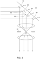
- the controller 38 may send a signal 48 to a laser source 28 to selectively melt the top layer 44 by use of an array 12 of small, individually directed mirrors.
- a wide laser beam 18, or similar illumination e.g. can be from multiple laser sources
- the laser beam 18 or beams may have a power of from about 10 to 60 W.
- Groups of mirrors e.g. 9 to 25 mirrors
- Another group of mirrors for example another group of 9-25 mirrors, may direct the laser power from the array 12 to an adjacent spot.
- This grouping of mirrors may be used to direct the laser power to multiple spots in the pattern, for example enough spots to form the entire pattern, so that the multiple spots of the pattern may be formed simultaneously. In this manner, a larger percentage (e.g. over 10%) to as much as the full pattern (depending on complexity of the layer) may be illuminated simultaneously. This may reduce the layer melt time for the entire layer 40 of the workpiece 36 to under one second.
- the next layer 44 of powder can then be spread over the build surface 46, for example by the wiper 26 or by for example a fluidized bed where the workpiece 36 is lowered into the powder bed by a small step, i.e. by the thickness of the next layer 40.
- Each micro-mirror may be 0.5 to 0.9 mm in size.
- the typical power capacity for such mirrors is rated as 1 to 3 W depending on the coating and the laser wavelength.
- the array 12 can be repointed in a few more milliseconds to achieve over 4000 mm per second build rate.
- the array 12 may be an array of thin-film micro-mirrors and may have, for example, an array of 200 x 200 mirrors, each mirror being 0.5 to 0.9 mm in size.
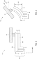
- each micro-mirror 80 may be formed of aluminum.
- the array 12 may use thin film piezoelectric actuators 82 in the form of micro-cantilevers.
- each mirror 80 may be connected to a cantilever 84 through a support post 86.
- the cantilevers 84 may be anchored to an underlying substrate.
- a cantilever 84 includes a supporting layer 88, a bottom electrode 90, a piezoelectric layer 92 and top electrode 94.
- the piezoelectric layer 92 layer shrinks in the horizontal direction and expands in the vertical direction. Since the neutral plane of the cantilever 84 shifts toward the bottom of the electrode 90 due to thickness of the supporting layer 88, the mechanical strain of the piezoelectric layer 92 causes vertical deflection delta 96 of the cantilever 84 and a tilt of angle alpha 98 of the mirror 80 on top of it.
- the mirrors in FIG. 2 are shown at various tilt angles in accordance with the energy distribution patterns determined by controller 38.
- FIGS. 2 and 3 show that the tilt angle alpha 98 of the mirror may be linearly proportional to the applied voltage within a voltage operating range.
- each layer 40 may be stored in the controller 38 and the mirrors 80 of the array 12 may be controlled by the controller to reflect the laser beam or beams 18 and direct the reflected beam or beams 58 onto the powder layer 44 provided over the build surface 46 in the shape of the next layer 40 to be fused (i.e. built).
- imaging optical components 18 provide control of laser beam homogenization and shaping.
- the controller 38 is provided a preselected pattern for each layer 40 and controls the array 12 to modify the beam or beams 18 from the laser source 28 to form the reflected, or output, beam or beams 58.
- the mirrors 80 are continuously moveable for reflecting varying amounts of energy from the laser source 28.
- the controller 38 may be configured to move the mirrors 80 to partially reflective positions to spatially vary the laser beam energy profile.
- a beam spatial profile measurement 122 is made and sent to the controller 38 and compared with a desired spatial profile.
- the controller 38 positions the mirrors 80 to set each mirror 80 to an angle that changes the amount of energy at melt spot in accordance with the desired beam profile.
- the desired profile is uniform across the beam 58 and the mirrors 80 are so set.
- the controller 38 may be configured to monitor the laser beam profile measurement 122 and adjust the array 12 in accordance with the desired profile. Adjustments can be rapidly made on a pulse-by-pulse basis.
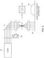
- the optical system may control the energy intensity through continuous changes of the reflection angle of each mirror 80 as shown in FIGS. 2 and 5 .
- the laser energy reflected on the mirror 80 forms an intensity image on the projection stop plane 62 and this image moves along the horizontal axis as the reflection angle changes.
- the system 20 can adjust the power distribution of one spot to the next in a continuous manner.
- the creation of a homogenized laser beam distribution profile 124 with the two-dimensional array 12 with continuously adjustable mirror positions may include all beam energy profiles, from a simple Gaussian shape to complex energy profiles are possible e.g. annular rings and multiple Gaussian beamlets with different peak energy intensities.
- the laser source may instead be any other source of energy beams capable of heating the powder to sufficient temperatures and at sufficient rates.
- Each beam may operate with different frequencies to meet manufacturing objectives. For example, beams with shorter wavelengths may heat up the powder faster than beams with longer wavelengths.
- Different optical frequencies or wavelengths typically requires different types of lasers; for example, CO 2 lasers, diode lasers, and fiber lasers.
- the wavelength, and thus the laser type, for heating and/or melting may be based on the composition of the powder (for example metal or ceramic or polymer). Particles of a powder may have different heat absorption rates impacting melting rates and solidification rates.
- wavelength other properties of the beam may be considered. For example, pulsed laser beams or continuous laser beams may be used to melt the powder.
- the present technology addresses the problem of the long build time for a part which can reach over 24 hours for even a small part.
- the operation is made parallel rather than a serial build of one point at a time as currently done.
- a technical advantage of the present technology is the highly parallel build of an additive part using a micro mirror array to create each segment of the built layer.
- Another technical advantage of the present technology is the ability to control heating and cooling rates by tailoring the laser energy power over time spectrum. Controlling cooling can be used to minimize cracking of some materials.
- a further technical advantage of the present technology is the elimination of geometric errors sometimes associated with scanning galvanometers when building a feature off to the side.
- An even further technical advantage of the present technology is the ability to form some difficult features such as overhang areas simultaneously which may reduce distortions of such features.
- Yet another technical advantage of the present technology is its use with a waterfall type powder delivery (powder falling in a thin sheet in front of a horizontally built part), as a full section would be created at one time. With a point scanning system there may be a need to reduce the speed of the scan to not move faster than the fall rate of the powder.
- a commercial advantage of the present technology is faster build rates.
- the present invention may be applicable to the build function on components, it should be appreciated that the present invention is applicable for the additive manufacturing repair of components.
Description
- The present technology relates generally to the use of a micro-mirror technology in additive manufacturing, for example Direct Metal Laser Melting (DMLM) systems and processes, to allow for the creation of full patterns simultaneously to facilitate higher build speeds.
- Additive manufacturing is a technology that enables the "3D-printing" of components of various materials including metals, ceramics and plastics. In additive manufacturing, a part is built in a layer-by-layer manner by leveling, for example, metal powder and selectively fusing the powder within a layer using a high-power laser or electron beam. After each layer, more powder is added and the laser patterns the next layer, simultaneously fusing it to the prior layers to fabricate a complete component buried in a powder bed. Additive manufacturing systems and processes are used to fabricate precision three-dimensional components from a digital model.
- Current systems and processes are limited in speed by the time needed to fully scan out each part layer in a serial manner using a single scanning mirror to direct a high power laser beam along the outline of one layer of the part to be made. Once the outline of the part is complete, the scanner directs the beam to the region between the inner and outer walls to fill in the material. In each process, the laser melts a thin layer of powdered metal to melt the metal onto the previous layer produced. Once a layer is made, a recoater bar moves across and adds another layer of powder and the process with the laser is repeated. Each layer can take several seconds to a few minute to complete with many thousands of layers needed to make a part.
- An alternate way to build a full section at a time is to use a mask which only lets a small area of a wide beam to the powder at one time. A disadvantage of this approach is it is very laser power inefficient, requiring the dumping of most of the laser power.
- In making a build in current powder bed systems, the laser beam or electron beam is used to scan a layer of powder to sinter and melt the desired pattern in the layers of the powder bed. The typical scanning time for such systems per layer is in the range of 70-100 seconds. For some applications, the build can require days of processing time. One application of DMLM is in the fabrication and repair of airfoils for gas turbine engines for aircraft. The geometries of the airfoils are difficult to form using conventional casting technologies, thus fabrication of the airfoils using a DMLM process or an electron-beam melting process has been proposed. With the layers built upon one another and joined to one another cross-section by cross-section, an airfoil or portion thereof, such as for a repair, with the required geometries, may be produced. The airfoil may require post-processing to provide desired structural characteristics.
-
US 2003/052105 A1 andWO 2016/075801 A1 disclose prior art methods and systems and provide the basis for the preamble of the independent claims. - The invention provides an additive manufacturing method according to claim 1 as well as an additive manufacturing system according to claim 8.
- These and other features, aspects, and advantages of the present invention will become better understood when the following detailed description is read with reference to the accompanying drawings in which like characters represent like parts throughout the drawings, wherein:
-
FIG. 1 schematically depicts a DMLM system according to an example of the present invention; -
FIG. 2 schematically depicts an array of micro-mirrors according to an example of the present invention; -
FIG. 3 schematically depicts an individual micro-mirror of the array according to an example of the present invention; -
FIG. 4 schematically depicts the micro-mirror ofFIG. 3 in a tilted position; and -
FIG. 5 schematically depicts a portion of the system ofFIG. 1 for forming a desired beam profile. - Referring to
FIG. 1 , anadditive manufacturing system 20, for example aDMLM system 20 includes a build table 22 for holding apowder bed 24, a particle spreader or wiper orrecoater bar 26 for spreading thepowder bed 24 over the build table 22, apowder supply hopper 30 for supplying powder to thespreader 26, and apowder surplus hopper 32. Theadditive manufacturing system 20 may be configured to build or repair aworkpiece 36 in a layer-by-layer fashion. - A
controller 38 may have an integral CAD system for modeling theworkpiece 36 into a plurality oflayers 40 additively built atop one another generally in a vertical or z-coordinate direction (see arrow 42). As manufactured, eachsolidified layer 40 corresponds to a layer 44 of thepowder bed 24 prior to solidification. The powder bed layer 44 is placed on top of abuild surface 46 of the previously solidifiedlayer 40. Thecontroller 38 is configured to operate thesystem 20 through a series of electrical and/ordigital signals 48 sent to thesystem 20 components. For example, thecontroller 38 may send asignal 48 to apiston 50 of the supply hopper 30 to sequentially push asupply powder 52 upward for receipt by thespreader 26, or alternatively or in addition thereto, thesupply hopper 30 may feed powder downward via gravity. Thespreader 26 may be a wiper, roller or other device that pushes the powder bed layer 44 in thedirection 54 or otherwise places thesupply powder 52 over thebuild surface 46 of theworkpiece 36 by a predetermined thickness established throughdownward movement 42 of the build table 22 controlled by thecontroller 38. Anyexcess powder 56 may be pushed into thesurplus hopper 32 by thespreader 26. It should be appreciated that the powder bed layer 44 may not be composed of a powder but may take the form of any substrate that may be layed or applied across thebuild surface 46 in preparation for melting. - Once a substantially level powder layer 44 is established over the
build surface 46, thecontroller 38 may send asignal 48 to alaser source 28 to selectively melt the top layer 44 by use of anarray 12 of small, individually directed mirrors. Awide laser beam 18, or similar illumination (e.g. can be from multiple laser sources) is configured to illuminate thearray 12. Thelaser beam 18 or beams may have a power of from about 10 to 60 W. Groups of mirrors (e.g. 9 to 25 mirrors) can direct the laser power from thearray 12 to one spot on the full pattern of the powder bed layer 44 that is spread onto thebuild surface 46 by thewiper 26. Another group of mirrors, for example another group of 9-25 mirrors, may direct the laser power from thearray 12 to an adjacent spot. This grouping of mirrors may be used to direct the laser power to multiple spots in the pattern, for example enough spots to form the entire pattern, so that the multiple spots of the pattern may be formed simultaneously. In this manner, a larger percentage (e.g. over 10%) to as much as the full pattern (depending on complexity of the layer) may be illuminated simultaneously. This may reduce the layer melt time for theentire layer 40 of theworkpiece 36 to under one second. The next layer 44 of powder can then be spread over thebuild surface 46, for example by thewiper 26 or by for example a fluidized bed where theworkpiece 36 is lowered into the powder bed by a small step, i.e. by the thickness of thenext layer 40. Each micro-mirror may be 0.5 to 0.9 mm in size. The typical power capacity for such mirrors is rated as 1 to 3 W depending on the coating and the laser wavelength. For superalloy powders of about 10-60 µm particle sized, to melt one spot requires 10 to 25 W of power in a 0.1 mm spot. For an array of 200 x 200 mirrors, this would permit 1600 to 4000 spots to be illuminated simultaneously. This would be enough to create 20 to over 100 linear mm of a part wall in a few milliseconds. Thearray 12 can be repointed in a few more milliseconds to achieve over 4000 mm per second build rate. - Referring to
FIGS. 1-4 , thearray 12 may be an array of thin-film micro-mirrors and may have, for example, an array of 200 x 200 mirrors, each mirror being 0.5 to 0.9 mm in size. Referring toFIGS. 3 and 4 , each micro-mirror 80 may be formed of aluminum. Thearray 12 may use thin filmpiezoelectric actuators 82 in the form of micro-cantilevers. As shown inFIGS. 3 and 4 , eachmirror 80 may be connected to acantilever 84 through asupport post 86. Thecantilevers 84 may be anchored to an underlying substrate. Acantilever 84 includes a supportinglayer 88, abottom electrode 90, apiezoelectric layer 92 andtop electrode 94. When an electric field is applied between theelectrodes piezoelectric layer 92 layer shrinks in the horizontal direction and expands in the vertical direction. Since the neutral plane of thecantilever 84 shifts toward the bottom of theelectrode 90 due to thickness of the supportinglayer 88, the mechanical strain of thepiezoelectric layer 92 causesvertical deflection delta 96 of thecantilever 84 and a tilt of angle alpha 98 of themirror 80 on top of it. The mirrors inFIG. 2 are shown at various tilt angles in accordance with the energy distribution patterns determined bycontroller 38.FIGS. 2 and3 show that the tilt angle alpha 98 of the mirror may be linearly proportional to the applied voltage within a voltage operating range. - The pattern, or outline, of each
layer 40 may be stored in thecontroller 38 and themirrors 80 of thearray 12 may be controlled by the controller to reflect the laser beam or beams 18 and direct the reflected beam or beams 58 onto the powder layer 44 provided over thebuild surface 46 in the shape of thenext layer 40 to be fused (i.e. built). For operation with thelaser source 26 and thearray 12, imagingoptical components 18 provide control of laser beam homogenization and shaping. As shown inFIG. 1 , thecontroller 38 is provided a preselected pattern for eachlayer 40 and controls thearray 12 to modify the beam or beams 18 from thelaser source 28 to form the reflected, or output, beam or beams 58. Themirrors 80 are continuously moveable for reflecting varying amounts of energy from thelaser source 28. Thecontroller 38 may be configured to move themirrors 80 to partially reflective positions to spatially vary the laser beam energy profile. - To homogenize the spatial intensity distribution of the
laser beam 18, a beamspatial profile measurement 122 is made and sent to thecontroller 38 and compared with a desired spatial profile. Thecontroller 38 positions themirrors 80 to set eachmirror 80 to an angle that changes the amount of energy at melt spot in accordance with the desired beam profile. To homogenize thebeam 58, the desired profile is uniform across thebeam 58 and themirrors 80 are so set. Thecontroller 38 may be configured to monitor the laserbeam profile measurement 122 and adjust thearray 12 in accordance with the desired profile. Adjustments can be rapidly made on a pulse-by-pulse basis. - The optical system may control the energy intensity through continuous changes of the reflection angle of each
mirror 80 as shown inFIGS. 2 and5 . The laser energy reflected on themirror 80 forms an intensity image on theprojection stop plane 62 and this image moves along the horizontal axis as the reflection angle changes. By changing the number of beams directed to one spot or series of spots, thesystem 20 can adjust the power distribution of one spot to the next in a continuous manner. The creation of a homogenized laserbeam distribution profile 124 with the two-dimensional array 12 with continuously adjustable mirror positions may include all beam energy profiles, from a simple Gaussian shape to complex energy profiles are possible e.g. annular rings and multiple Gaussian beamlets with different peak energy intensities. - It should be appreciated that the laser source may instead be any other source of energy beams capable of heating the powder to sufficient temperatures and at sufficient rates. Each beam may operate with different frequencies to meet manufacturing objectives. For example, beams with shorter wavelengths may heat up the powder faster than beams with longer wavelengths. Different optical frequencies or wavelengths typically requires different types of lasers; for example, CO2 lasers, diode lasers, and fiber lasers. The wavelength, and thus the laser type, for heating and/or melting may be based on the composition of the powder (for example metal or ceramic or polymer). Particles of a powder may have different heat absorption rates impacting melting rates and solidification rates. Besides wavelength, other properties of the beam may be considered. For example, pulsed laser beams or continuous laser beams may be used to melt the powder.
- The present technology addresses the problem of the long build time for a part which can reach over 24 hours for even a small part. By making the build with a series of laser pulses, each creating thousands of build points per second, the operation is made parallel rather than a serial build of one point at a time as currently done. A technical advantage of the present technology is the highly parallel build of an additive part using a micro mirror array to create each segment of the built layer. Another technical advantage of the present technology is the ability to control heating and cooling rates by tailoring the laser energy power over time spectrum. Controlling cooling can be used to minimize cracking of some materials. A further technical advantage of the present technology is the elimination of geometric errors sometimes associated with scanning galvanometers when building a feature off to the side. An even further technical advantage of the present technology is the ability to form some difficult features such as overhang areas simultaneously which may reduce distortions of such features. Yet another technical advantage of the present technology is its use with a waterfall type powder delivery (powder falling in a thin sheet in front of a horizontally built part), as a full section would be created at one time. With a point scanning system there may be a need to reduce the speed of the scan to not move faster than the fall rate of the powder. A commercial advantage of the present technology is faster build rates.
- Although the present invention may be applicable to the build function on components, it should be appreciated that the present invention is applicable for the additive manufacturing repair of components.
- It is to be understood that not necessarily all such objects or advantages described above may be achieved in accordance with any particular example. Thus, for example, those skilled in the art will recognize that the systems and techniques described herein may be embodied or carried out in a manner that achieves or optimizes one advantage or group of advantages as taught herein without necessarily achieving other objects or advantages as may be taught or suggested herein.
Claims (12)
- An additive manufacturing method, comprising:patterning a laser beam (18) using a mirror array (12); andreflecting the patterned laser beam (58) from the mirror array (12) onto a powder (44) to melt the powder, wherein the pattern corresponds to a portion of a layer (40) of an article, characterized in that the patterned laser beam (58) comprises a plurality of laser spots, and groups of 9-25 mirrors (80) are configured to provide each laser spot of the patterned laser beam.
- A method according to claim 1, further comprising:
spreading a layer of powder (44) over the layer (40) of the article after solidification of the layer of the article; wherein the method particularly further comprises adjusting a position of a build table (22) that supports the article. - A method according to claim 1, further comprising:
providing a desired distribution profile to the laser beam (18) - A method according to claim 3, further comprising:
controlling an energy intensity of the patterned beam (58) through changes of a reflection angle of each mirror (80). - A method according to claim 1, wherein a power capacity of each mirror (80) is 1 to 3 watts and the groups of mirrors (80) are configured to provide laser spots of 10 to 25 watts; wherein each laser spot is preferably 0.1 mm.
- A method according to claim 1, wherein the pattern corresponds to a 10% to 100% of the layer of the article.
- A method according to claim 1, wherein the powder (52) is a superalloy having a particle size of 10 to 60 µm.
- An additive manufacturing system (20), comprising:a build table (22) configured to support an article to be manufactured from powder;a laser source (28) configured to generate a laser beam (18); anda mirror array (12) configured to pattern the laser beam (18) and reflect the patterned laser beam (58) onto the powder (24) to melt the powder, wherein the pattern corresponds to a portion of a layer (40) of the article, characterized in that the patterned laser beam (58) comprises a plurality of laser spots, and groups of 9-25 mirrors (80) are configured to provide each laser spot of the patterned laser beam
- A system according to claim 8, further comprising:
a powder spreader (26) configured to spread a layer of powder (44) over the layer (40) of the article after solidification of the layer of the article; wherein the build table (22) is particularly configured to move to adjust a position of the build table (22) relative to the powder spreader (26). - A system according to claim 8, further comprising:
an optical system configured to provide a desired distribution profile to the laser beam; wherein the optical system is particularly further configured to control an energy intensity of the patterned beam (58) through changes of a reflection angle of each mirror (80). - A system according to claim 8, wherein a power capacity of each mirror (80) is 1 to 3 watts and the groups of mirrors (80) are configured to provide laser spots of 10 to 25 watts; wherein each laser spot is particularly 0.1 mm.
- A system according to claim 8, wherein the pattern corresponds to a 10% to 100% of the layer (40) of the article.
Priority Applications (1)
| Application Number | Priority Date | Filing Date | Title |
|---|---|---|---|
| EP23201665.9A EP4279274A3 (en) | 2016-12-14 | 2017-11-30 | Additive manufacturing systems and methods |
Applications Claiming Priority (2)
| Application Number | Priority Date | Filing Date | Title |
|---|---|---|---|
| US15/378,116 US10399179B2 (en) | 2016-12-14 | 2016-12-14 | Additive manufacturing systems and methods |
| PCT/US2017/063874 WO2018111564A1 (en) | 2016-12-14 | 2017-11-30 | Additive manufacturing systems and methods |
Related Child Applications (1)
| Application Number | Title | Priority Date | Filing Date |
|---|---|---|---|
| EP23201665.9A Division EP4279274A3 (en) | 2016-12-14 | 2017-11-30 | Additive manufacturing systems and methods |
Publications (3)
| Publication Number | Publication Date |
|---|---|
| EP3554749A1 EP3554749A1 (en) | 2019-10-23 |
| EP3554749A4 EP3554749A4 (en) | 2020-08-05 |
| EP3554749B1 true EP3554749B1 (en) | 2023-11-01 |
Family
ID=62488624
Family Applications (2)
| Application Number | Title | Priority Date | Filing Date |
|---|---|---|---|
| EP23201665.9A Pending EP4279274A3 (en) | 2016-12-14 | 2017-11-30 | Additive manufacturing systems and methods |
| EP17880406.8A Active EP3554749B1 (en) | 2016-12-14 | 2017-11-30 | Additive manufacturing systems and methods |
Family Applications Before (1)
| Application Number | Title | Priority Date | Filing Date |
|---|---|---|---|
| EP23201665.9A Pending EP4279274A3 (en) | 2016-12-14 | 2017-11-30 | Additive manufacturing systems and methods |
Country Status (4)
| Country | Link |
|---|---|
| US (1) | US10399179B2 (en) |
| EP (2) | EP4279274A3 (en) |
| CN (1) | CN110366462A (en) |
| WO (1) | WO2018111564A1 (en) |
Families Citing this family (11)
| Publication number | Priority date | Publication date | Assignee | Title |
|---|---|---|---|---|
| DE102015211999A1 (en) * | 2015-06-29 | 2016-12-29 | Trumpf Werkzeugmaschinen Gmbh + Co. Kg | Laser processing head and laser processing machine with it |
| US10500832B2 (en) * | 2017-01-18 | 2019-12-10 | General Electric Company | Systems and methods for additive manufacturing rotating build platforms |
| GB201807830D0 (en) * | 2018-05-15 | 2018-06-27 | Renishaw Plc | Laser beam scanner |
| US10960607B2 (en) | 2018-12-13 | 2021-03-30 | General Electric Company | Systems and methods for monitoring powder spreading in additive manufacturing systems |
| CA3127485A1 (en) * | 2019-01-24 | 2020-07-30 | Walter Voit | Systems, methods, and materials for ultra-high throughput additive manufacturing |
| US11745289B2 (en) | 2019-02-21 | 2023-09-05 | General Electric Company | Additive manufacturing systems and methods including rotating build platform |
| US11254053B2 (en) | 2019-02-28 | 2022-02-22 | 3D Systems, Inc. | High resolution three-dimensional printing system |
| US11858202B2 (en) * | 2019-03-26 | 2024-01-02 | Lawrence Livermore National Security, Llc | System and method for performing laser powder bed fusion using controlled, supplemental in situ surface heating to control microstructure and residual stresses in formed part |
| CN110142405B (en) * | 2019-03-29 | 2021-06-18 | 西北大学 | Two-dimensional area array laser 3D metal printer and file conversion and printing control method thereof |
| US11872760B2 (en) | 2020-10-29 | 2024-01-16 | Seurat Technologies, Inc. | Distributed flux array |
| US20230347452A1 (en) * | 2022-04-28 | 2023-11-02 | Raytheon Technologies Corporation | Off-axis laser beam measurement for laser powder bed fusion |
Citations (1)
| Publication number | Priority date | Publication date | Assignee | Title |
|---|---|---|---|---|
| US20020008091A1 (en) * | 2000-05-25 | 2002-01-24 | Brandinger Jay J. | Laser beam shaping device and apparatus for material machining |
Family Cites Families (41)
| Publication number | Priority date | Publication date | Assignee | Title |
|---|---|---|---|---|
| WO1988002677A2 (en) | 1986-10-17 | 1988-04-21 | Board Of Regents, The University Of Texas System | Method and apparatus for producing parts by selective sintering |
| CA2108761A1 (en) * | 1992-10-23 | 1994-04-24 | Koichi Haruta | Method and apparatus for welding material by laser beam |
| US6542179B1 (en) | 1998-09-30 | 2003-04-01 | Eastman Kodak Company | Light integrating system with reduced dynamic shading |
| US6002507A (en) | 1998-12-01 | 1999-12-14 | Xerox Corpoation | Method and apparatus for an integrated laser beam scanner |
| US20020071169A1 (en) | 2000-02-01 | 2002-06-13 | Bowers John Edward | Micro-electro-mechanical-system (MEMS) mirror device |
| KR20030078895A (en) | 2001-01-25 | 2003-10-08 | 일진다이아몬드 주식회사 서울지사 | Image compensation methods and apparatus using correction zones |
| US6618184B2 (en) | 2001-04-03 | 2003-09-09 | Agere Systems Inc. | Device for use with a micro-electro-mechanical system (MEMS) optical device and a method of manufacture therefor |
| US6704476B2 (en) | 2001-06-29 | 2004-03-09 | Lucent Technologies Inc. | Optical MEMS switch with imaging system |
| JP2003080604A (en) * | 2001-09-10 | 2003-03-19 | Fuji Photo Film Co Ltd | Laminate shaping apparatus |
| TWI230544B (en) | 2002-07-25 | 2005-04-01 | Veutron Corp | Light source control method and apparatus of image scanner |
| WO2004083778A1 (en) | 2003-03-18 | 2004-09-30 | Hermary Alexander Thomas | Coded-light dual-view profile scanner |
| US7007843B2 (en) | 2003-06-09 | 2006-03-07 | Symbol Technologies, Inc. | Light beam shaping arrangement and method in electro-optical readers |
| US6995830B2 (en) | 2003-12-22 | 2006-02-07 | Asml Netherlands B.V. | Lithographic projection apparatus and device manufacturing method |
| US7923306B2 (en) | 2004-06-18 | 2011-04-12 | Electro Scientific Industries, Inc. | Semiconductor structure processing using multiple laser beam spots |
| CN1603031A (en) * | 2004-11-05 | 2005-04-06 | 华南理工大学 | Selected zone laser melting and rapid forming method for metal parts and apparatus thereof |
| JP4854061B2 (en) | 2005-01-14 | 2012-01-11 | 日東電工株式会社 | Manufacturing method of laser processed product and protective sheet for laser processing |
| US7262408B2 (en) | 2005-06-15 | 2007-08-28 | Board Of Trustees Of Michigan State University | Process and apparatus for modifying a surface in a work region |
| US8102580B2 (en) | 2006-01-30 | 2012-01-24 | Duncan Wayne O | Scanning illumination system and method |
| US8488895B2 (en) | 2006-05-31 | 2013-07-16 | Indiana University Research And Technology Corp. | Laser scanning digital camera with pupil periphery illumination and potential for multiply scattered light imaging |
| KR100696165B1 (en) | 2006-08-28 | 2007-03-20 | 엠텍비젼 주식회사 | Image brightness compensating apparatus and method, recorded medium recorded the program performing it |
| US7843633B2 (en) * | 2007-01-15 | 2010-11-30 | Sumitomo Electric Industries, Ltd. | Laser processing apparatus |
| EP2208354A4 (en) | 2007-10-10 | 2010-12-22 | Gerard Dirk Smits | Image projector with reflected light tracking |
| WO2009054445A1 (en) * | 2007-10-26 | 2009-04-30 | Panasonic Electric Works Co., Ltd. | Production device and production method of metal powder sintered component |
| TWI394443B (en) | 2008-09-19 | 2013-04-21 | Altek Corp | Image brightness correction method |
| ES2700454T5 (en) | 2009-04-28 | 2022-02-28 | Bae Systems Plc | Manufacturing method by adding successive layers |
| US8922780B2 (en) | 2009-05-14 | 2014-12-30 | Andover Photonics, Inc. | Shape measurement using microchip based fringe projection |
| JP5588310B2 (en) | 2009-11-15 | 2014-09-10 | プライムセンス リミテッド | Optical projector with beam monitor |
| CN103358555A (en) | 2012-03-30 | 2013-10-23 | 通用电气公司 | Multi-beam laser scanning system and method for laser rapid prototyping processing equipment |
| US9266192B2 (en) | 2012-05-29 | 2016-02-23 | Electro Scientific Industries, Inc. | Method and apparatus for processing workpieces |
| US9238577B2 (en) | 2012-09-21 | 2016-01-19 | The University Of North Carolina At Charlotte | Dynamic laser beam shaping methods and systems |
| US20140246809A1 (en) | 2013-03-04 | 2014-09-04 | California Institute Of Technology | Systems and methods implementing additive manufacturing processes that utilize multiple build heads |
| JP6359640B2 (en) | 2013-04-26 | 2018-07-18 | ユナイテッド テクノロジーズ コーポレイションUnited Technologies Corporation | Selective laser melting system |
| WO2014179679A1 (en) | 2013-05-03 | 2014-11-06 | United Technologies Corporation | Method of eliminating sub-surface porosity |
| CN103341625B (en) * | 2013-07-10 | 2015-05-13 | 湖南航天工业总公司 | 3D printing manufacturing device and method of metal parts |
| GB201316815D0 (en) * | 2013-09-23 | 2013-11-06 | Renishaw Plc | Additive manufacturing apparatus and method |
| US10532556B2 (en) * | 2013-12-16 | 2020-01-14 | General Electric Company | Control of solidification in laser powder bed fusion additive manufacturing using a diode laser fiber array |
| EP3705300A1 (en) | 2013-12-17 | 2020-09-09 | EOS GmbH Electro Optical Systems | Laser printing system |
| US9999924B2 (en) | 2014-08-22 | 2018-06-19 | Sigma Labs, Inc. | Method and system for monitoring additive manufacturing processes |
| US20170304895A1 (en) | 2014-10-01 | 2017-10-26 | Renishaw Plc | Additive manufacturing apparatus and method |
| JP6840540B2 (en) | 2014-11-14 | 2021-03-10 | 株式会社ニコン | Modeling equipment |
| JP2018524178A (en) * | 2015-06-10 | 2018-08-30 | アイピージー フォトニクス コーポレーション | Multiple beam additive manufacturing |
-
2016
- 2016-12-14 US US15/378,116 patent/US10399179B2/en active Active
-
2017
- 2017-11-30 EP EP23201665.9A patent/EP4279274A3/en active Pending
- 2017-11-30 EP EP17880406.8A patent/EP3554749B1/en active Active
- 2017-11-30 CN CN201780085902.1A patent/CN110366462A/en active Pending
- 2017-11-30 WO PCT/US2017/063874 patent/WO2018111564A1/en unknown
Patent Citations (1)
| Publication number | Priority date | Publication date | Assignee | Title |
|---|---|---|---|---|
| US20020008091A1 (en) * | 2000-05-25 | 2002-01-24 | Brandinger Jay J. | Laser beam shaping device and apparatus for material machining |
Also Published As
| Publication number | Publication date |
|---|---|
| EP3554749A1 (en) | 2019-10-23 |
| EP4279274A2 (en) | 2023-11-22 |
| US20180161925A1 (en) | 2018-06-14 |
| US10399179B2 (en) | 2019-09-03 |
| WO2018111564A1 (en) | 2018-06-21 |
| EP3554749A4 (en) | 2020-08-05 |
| CN110366462A (en) | 2019-10-22 |
| EP4279274A3 (en) | 2023-11-29 |
Similar Documents
| Publication | Publication Date | Title |
|---|---|---|
| EP3554749B1 (en) | Additive manufacturing systems and methods | |
| EP3102389B1 (en) | An additive manufacturing system with a multi-laser beam gun and method of operation | |
| US11027536B2 (en) | Diode laser fiber array for powder bed fabrication or repair | |
| CN105562688B (en) | Production of components by selective laser melting | |
| US10195692B2 (en) | Parallel direct metal laser melting | |
| CN110267796B (en) | Additive manufacturing system and method | |
| US11712765B2 (en) | Diode laser fiber array for contour of powder bed fabrication or repair | |
| US11084097B2 (en) | Additive manufacturing with cell processing recipes | |
| JP2020514140A (en) | Material preheating in additive manufacturing equipment | |
| EP3434396A1 (en) | Pre-fusion laser sintering for metal powder stabilization during additive manufacturing | |
| US20220097174A1 (en) | Variable beam geometry laser-based powder bed fusion | |
| EP3694662A1 (en) | Apparatus and method for producing three-dimensional work pieces |
Legal Events
| Date | Code | Title | Description |
|---|---|---|---|
| STAA | Information on the status of an ep patent application or granted ep patent |
Free format text: STATUS: THE INTERNATIONAL PUBLICATION HAS BEEN MADE |
|
| PUAI | Public reference made under article 153(3) epc to a published international application that has entered the european phase |
Free format text: ORIGINAL CODE: 0009012 |
|
| STAA | Information on the status of an ep patent application or granted ep patent |
Free format text: STATUS: REQUEST FOR EXAMINATION WAS MADE |
|
| 17P | Request for examination filed |
Effective date: 20190614 |
|
| AK | Designated contracting states |
Kind code of ref document: A1 Designated state(s): AL AT BE BG CH CY CZ DE DK EE ES FI FR GB GR HR HU IE IS IT LI LT LU LV MC MK MT NL NO PL PT RO RS SE SI SK SM TR |
|
| AX | Request for extension of the european patent |
Extension state: BA ME |
|
| DAV | Request for validation of the european patent (deleted) | ||
| DAX | Request for extension of the european patent (deleted) | ||
| A4 | Supplementary search report drawn up and despatched |
Effective date: 20200702 |
|
| RIC1 | Information provided on ipc code assigned before grant |
Ipc: B22F 3/105 20060101AFI20200626BHEP Ipc: B33Y 10/00 20150101ALI20200626BHEP Ipc: B33Y 30/00 20150101ALI20200626BHEP |
|
| GRAP | Despatch of communication of intention to grant a patent |
Free format text: ORIGINAL CODE: EPIDOSNIGR1 |
|
| STAA | Information on the status of an ep patent application or granted ep patent |
Free format text: STATUS: GRANT OF PATENT IS INTENDED |
|
| INTG | Intention to grant announced |
Effective date: 20230526 |
|
| P01 | Opt-out of the competence of the unified patent court (upc) registered |
Effective date: 20230530 |
|
| GRAS | Grant fee paid |
Free format text: ORIGINAL CODE: EPIDOSNIGR3 |
|
| GRAA | (expected) grant |
Free format text: ORIGINAL CODE: 0009210 |
|
| STAA | Information on the status of an ep patent application or granted ep patent |
Free format text: STATUS: THE PATENT HAS BEEN GRANTED |
|
| AK | Designated contracting states |
Kind code of ref document: B1 Designated state(s): AL AT BE BG CH CY CZ DE DK EE ES FI FR GB GR HR HU IE IS IT LI LT LU LV MC MK MT NL NO PL PT RO RS SE SI SK SM TR |
|
| REG | Reference to a national code |
Ref country code: GB Ref legal event code: FG4D |
|
| REG | Reference to a national code |
Ref country code: CH Ref legal event code: EP |
|
| REG | Reference to a national code |
Ref country code: IE Ref legal event code: FG4D |
|
| REG | Reference to a national code |
Ref country code: DE Ref legal event code: R096 Ref document number: 602017076153 Country of ref document: DE |
|
| PGFP | Annual fee paid to national office [announced via postgrant information from national office to epo] |
Ref country code: DE Payment date: 20231019 Year of fee payment: 7 |
|
| REG | Reference to a national code |
Ref country code: LT Ref legal event code: MG9D |
|
| REG | Reference to a national code |
Ref country code: NL Ref legal event code: MP Effective date: 20231101 |
|
| PG25 | Lapsed in a contracting state [announced via postgrant information from national office to epo] |
Ref country code: GR Free format text: LAPSE BECAUSE OF FAILURE TO SUBMIT A TRANSLATION OF THE DESCRIPTION OR TO PAY THE FEE WITHIN THE PRESCRIBED TIME-LIMIT Effective date: 20240202 |
|
| PG25 | Lapsed in a contracting state [announced via postgrant information from national office to epo] |
Ref country code: IS Free format text: LAPSE BECAUSE OF FAILURE TO SUBMIT A TRANSLATION OF THE DESCRIPTION OR TO PAY THE FEE WITHIN THE PRESCRIBED TIME-LIMIT Effective date: 20240301 |
|
| PG25 | Lapsed in a contracting state [announced via postgrant information from national office to epo] |
Ref country code: LT Free format text: LAPSE BECAUSE OF FAILURE TO SUBMIT A TRANSLATION OF THE DESCRIPTION OR TO PAY THE FEE WITHIN THE PRESCRIBED TIME-LIMIT Effective date: 20231101 |
|
| REG | Reference to a national code |
Ref country code: AT Ref legal event code: MK05 Ref document number: 1626632 Country of ref document: AT Kind code of ref document: T Effective date: 20231101 |
|
| PG25 | Lapsed in a contracting state [announced via postgrant information from national office to epo] |
Ref country code: NL Free format text: LAPSE BECAUSE OF FAILURE TO SUBMIT A TRANSLATION OF THE DESCRIPTION OR TO PAY THE FEE WITHIN THE PRESCRIBED TIME-LIMIT Effective date: 20231101 |
|
| PG25 | Lapsed in a contracting state [announced via postgrant information from national office to epo] |
Ref country code: AT Free format text: LAPSE BECAUSE OF FAILURE TO SUBMIT A TRANSLATION OF THE DESCRIPTION OR TO PAY THE FEE WITHIN THE PRESCRIBED TIME-LIMIT Effective date: 20231101 |