EP3553819A2 - Mounting structures for integrated device packages - Google Patents
Mounting structures for integrated device packages Download PDFInfo
- Publication number
- EP3553819A2 EP3553819A2 EP19168428.1A EP19168428A EP3553819A2 EP 3553819 A2 EP3553819 A2 EP 3553819A2 EP 19168428 A EP19168428 A EP 19168428A EP 3553819 A2 EP3553819 A2 EP 3553819A2
- Authority
- EP
- European Patent Office
- Prior art keywords
- integrated device
- layer
- carrier
- die
- spacer
- Prior art date
- Legal status (The legal status is an assumption and is not a legal conclusion. Google has not performed a legal analysis and makes no representation as to the accuracy of the status listed.)
- Granted
Links
Images










Classifications
-
- H—ELECTRICITY
- H10—SEMICONDUCTOR DEVICES; ELECTRIC SOLID-STATE DEVICES NOT OTHERWISE PROVIDED FOR
- H10W—GENERIC PACKAGES, INTERCONNECTIONS, CONNECTORS OR OTHER CONSTRUCTIONAL DETAILS OF DEVICES COVERED BY CLASS H10
- H10W40/00—Arrangements for thermal protection or thermal control
- H10W40/40—Arrangements for thermal protection or thermal control involving heat exchange by flowing fluids
- H10W40/47—Arrangements for thermal protection or thermal control involving heat exchange by flowing fluids by flowing liquids, e.g. forced water cooling
-
- B—PERFORMING OPERATIONS; TRANSPORTING
- B81—MICROSTRUCTURAL TECHNOLOGY
- B81B—MICROSTRUCTURAL DEVICES OR SYSTEMS, e.g. MICROMECHANICAL DEVICES
- B81B7/00—Microstructural systems ; Auxiliary parts of microstructural devices or systems
- B81B7/0032—Packages or encapsulation
- B81B7/0045—Packages or encapsulation for reducing stress inside of the package structure
- B81B7/0054—Packages or encapsulation for reducing stress inside of the package structure between other parts not provided for in B81B7/0048 - B81B7/0051
-
- H—ELECTRICITY
- H10—SEMICONDUCTOR DEVICES; ELECTRIC SOLID-STATE DEVICES NOT OTHERWISE PROVIDED FOR
- H10P—GENERIC PROCESSES OR APPARATUS FOR THE MANUFACTURE OR TREATMENT OF DEVICES COVERED BY CLASS H10
- H10P52/00—Grinding, lapping or polishing of wafers, substrates or parts of devices
-
- H—ELECTRICITY
- H10—SEMICONDUCTOR DEVICES; ELECTRIC SOLID-STATE DEVICES NOT OTHERWISE PROVIDED FOR
- H10P—GENERIC PROCESSES OR APPARATUS FOR THE MANUFACTURE OR TREATMENT OF DEVICES COVERED BY CLASS H10
- H10P54/00—Cutting or separating of wafers, substrates or parts of devices
-
- H—ELECTRICITY
- H10—SEMICONDUCTOR DEVICES; ELECTRIC SOLID-STATE DEVICES NOT OTHERWISE PROVIDED FOR
- H10W—GENERIC PACKAGES, INTERCONNECTIONS, CONNECTORS OR OTHER CONSTRUCTIONAL DETAILS OF DEVICES COVERED BY CLASS H10
- H10W42/00—Arrangements for protection of devices
- H10W42/20—Arrangements for protection of devices protecting against electromagnetic or particle radiation, e.g. light, X-rays, gamma-rays or electrons
-
- H—ELECTRICITY
- H10—SEMICONDUCTOR DEVICES; ELECTRIC SOLID-STATE DEVICES NOT OTHERWISE PROVIDED FOR
- H10W—GENERIC PACKAGES, INTERCONNECTIONS, CONNECTORS OR OTHER CONSTRUCTIONAL DETAILS OF DEVICES COVERED BY CLASS H10
- H10W70/00—Package substrates; Interposers; Redistribution layers [RDL]
- H10W70/60—Insulating or insulated package substrates; Interposers; Redistribution layers
- H10W70/611—Insulating or insulated package substrates; Interposers; Redistribution layers for connecting multiple chips together
-
- H—ELECTRICITY
- H10—SEMICONDUCTOR DEVICES; ELECTRIC SOLID-STATE DEVICES NOT OTHERWISE PROVIDED FOR
- H10W—GENERIC PACKAGES, INTERCONNECTIONS, CONNECTORS OR OTHER CONSTRUCTIONAL DETAILS OF DEVICES COVERED BY CLASS H10
- H10W70/00—Package substrates; Interposers; Redistribution layers [RDL]
- H10W70/60—Insulating or insulated package substrates; Interposers; Redistribution layers
- H10W70/62—Insulating or insulated package substrates; Interposers; Redistribution layers characterised by their interconnections
- H10W70/63—Vias, e.g. via plugs
- H10W70/635—Through-vias
-
- H—ELECTRICITY
- H10—SEMICONDUCTOR DEVICES; ELECTRIC SOLID-STATE DEVICES NOT OTHERWISE PROVIDED FOR
- H10W—GENERIC PACKAGES, INTERCONNECTIONS, CONNECTORS OR OTHER CONSTRUCTIONAL DETAILS OF DEVICES COVERED BY CLASS H10
- H10W70/00—Package substrates; Interposers; Redistribution layers [RDL]
- H10W70/60—Insulating or insulated package substrates; Interposers; Redistribution layers
- H10W70/67—Insulating or insulated package substrates; Interposers; Redistribution layers characterised by their insulating layers or insulating parts
- H10W70/68—Shapes or dispositions thereof
- H10W70/685—Shapes or dispositions thereof comprising multiple insulating layers
-
- H—ELECTRICITY
- H10—SEMICONDUCTOR DEVICES; ELECTRIC SOLID-STATE DEVICES NOT OTHERWISE PROVIDED FOR
- H10W—GENERIC PACKAGES, INTERCONNECTIONS, CONNECTORS OR OTHER CONSTRUCTIONAL DETAILS OF DEVICES COVERED BY CLASS H10
- H10W72/00—Interconnections or connectors in packages
- H10W72/701—Tape-automated bond [TAB] connectors
-
- H—ELECTRICITY
- H10—SEMICONDUCTOR DEVICES; ELECTRIC SOLID-STATE DEVICES NOT OTHERWISE PROVIDED FOR
- H10W—GENERIC PACKAGES, INTERCONNECTIONS, CONNECTORS OR OTHER CONSTRUCTIONAL DETAILS OF DEVICES COVERED BY CLASS H10
- H10W90/00—Package configurations
-
- H—ELECTRICITY
- H10—SEMICONDUCTOR DEVICES; ELECTRIC SOLID-STATE DEVICES NOT OTHERWISE PROVIDED FOR
- H10W—GENERIC PACKAGES, INTERCONNECTIONS, CONNECTORS OR OTHER CONSTRUCTIONAL DETAILS OF DEVICES COVERED BY CLASS H10
- H10W90/00—Package configurations
- H10W90/20—Configurations of stacked chips
- H10W90/293—Configurations of stacked chips characterised by non-galvanic coupling between the chips, e.g. capacitive coupling
-
- B—PERFORMING OPERATIONS; TRANSPORTING
- B81—MICROSTRUCTURAL TECHNOLOGY
- B81B—MICROSTRUCTURAL DEVICES OR SYSTEMS, e.g. MICROMECHANICAL DEVICES
- B81B2207/00—Microstructural systems or auxiliary parts thereof
- B81B2207/01—Microstructural systems or auxiliary parts thereof comprising a micromechanical device connected to control or processing electronics, i.e. Smart-MEMS
- B81B2207/012—Microstructural systems or auxiliary parts thereof comprising a micromechanical device connected to control or processing electronics, i.e. Smart-MEMS the micromechanical device and the control or processing electronics being separate parts in the same package
-
- B—PERFORMING OPERATIONS; TRANSPORTING
- B81—MICROSTRUCTURAL TECHNOLOGY
- B81C—PROCESSES OR APPARATUS SPECIALLY ADAPTED FOR THE MANUFACTURE OR TREATMENT OF MICROSTRUCTURAL DEVICES OR SYSTEMS
- B81C2203/00—Forming microstructural systems
- B81C2203/03—Bonding two components
- B81C2203/032—Gluing
-
- H—ELECTRICITY
- H10—SEMICONDUCTOR DEVICES; ELECTRIC SOLID-STATE DEVICES NOT OTHERWISE PROVIDED FOR
- H10W—GENERIC PACKAGES, INTERCONNECTIONS, CONNECTORS OR OTHER CONSTRUCTIONAL DETAILS OF DEVICES COVERED BY CLASS H10
- H10W70/00—Package substrates; Interposers; Redistribution layers [RDL]
- H10W70/40—Leadframes
- H10W70/411—Chip-supporting parts, e.g. die pads
- H10W70/415—Leadframe inner leads serving as die pads
-
- H—ELECTRICITY
- H10—SEMICONDUCTOR DEVICES; ELECTRIC SOLID-STATE DEVICES NOT OTHERWISE PROVIDED FOR
- H10W—GENERIC PACKAGES, INTERCONNECTIONS, CONNECTORS OR OTHER CONSTRUCTIONAL DETAILS OF DEVICES COVERED BY CLASS H10
- H10W70/00—Package substrates; Interposers; Redistribution layers [RDL]
- H10W70/40—Leadframes
- H10W70/411—Chip-supporting parts, e.g. die pads
- H10W70/417—Bonding materials between chips and die pads
-
- H—ELECTRICITY
- H10—SEMICONDUCTOR DEVICES; ELECTRIC SOLID-STATE DEVICES NOT OTHERWISE PROVIDED FOR
- H10W—GENERIC PACKAGES, INTERCONNECTIONS, CONNECTORS OR OTHER CONSTRUCTIONAL DETAILS OF DEVICES COVERED BY CLASS H10
- H10W72/00—Interconnections or connectors in packages
- H10W72/071—Connecting or disconnecting
- H10W72/073—Connecting or disconnecting of die-attach connectors
-
- H—ELECTRICITY
- H10—SEMICONDUCTOR DEVICES; ELECTRIC SOLID-STATE DEVICES NOT OTHERWISE PROVIDED FOR
- H10W—GENERIC PACKAGES, INTERCONNECTIONS, CONNECTORS OR OTHER CONSTRUCTIONAL DETAILS OF DEVICES COVERED BY CLASS H10
- H10W72/00—Interconnections or connectors in packages
- H10W72/071—Connecting or disconnecting
- H10W72/075—Connecting or disconnecting of bond wires
-
- H—ELECTRICITY
- H10—SEMICONDUCTOR DEVICES; ELECTRIC SOLID-STATE DEVICES NOT OTHERWISE PROVIDED FOR
- H10W—GENERIC PACKAGES, INTERCONNECTIONS, CONNECTORS OR OTHER CONSTRUCTIONAL DETAILS OF DEVICES COVERED BY CLASS H10
- H10W72/00—Interconnections or connectors in packages
- H10W72/30—Die-attach connectors
- H10W72/351—Materials of die-attach connectors
- H10W72/353—Materials of die-attach connectors not comprising solid metals or solid metalloids, e.g. ceramics
- H10W72/354—Materials of die-attach connectors not comprising solid metals or solid metalloids, e.g. ceramics comprising polymers
-
- H—ELECTRICITY
- H10—SEMICONDUCTOR DEVICES; ELECTRIC SOLID-STATE DEVICES NOT OTHERWISE PROVIDED FOR
- H10W—GENERIC PACKAGES, INTERCONNECTIONS, CONNECTORS OR OTHER CONSTRUCTIONAL DETAILS OF DEVICES COVERED BY CLASS H10
- H10W72/00—Interconnections or connectors in packages
- H10W72/30—Die-attach connectors
- H10W72/381—Auxiliary members
-
- H—ELECTRICITY
- H10—SEMICONDUCTOR DEVICES; ELECTRIC SOLID-STATE DEVICES NOT OTHERWISE PROVIDED FOR
- H10W—GENERIC PACKAGES, INTERCONNECTIONS, CONNECTORS OR OTHER CONSTRUCTIONAL DETAILS OF DEVICES COVERED BY CLASS H10
- H10W72/00—Interconnections or connectors in packages
- H10W72/60—Strap connectors, e.g. thick copper clips for grounding of power devices
-
- H—ELECTRICITY
- H10—SEMICONDUCTOR DEVICES; ELECTRIC SOLID-STATE DEVICES NOT OTHERWISE PROVIDED FOR
- H10W—GENERIC PACKAGES, INTERCONNECTIONS, CONNECTORS OR OTHER CONSTRUCTIONAL DETAILS OF DEVICES COVERED BY CLASS H10
- H10W72/00—Interconnections or connectors in packages
- H10W72/851—Dispositions of multiple connectors or interconnections
- H10W72/853—On the same surface
-
- H—ELECTRICITY
- H10—SEMICONDUCTOR DEVICES; ELECTRIC SOLID-STATE DEVICES NOT OTHERWISE PROVIDED FOR
- H10W—GENERIC PACKAGES, INTERCONNECTIONS, CONNECTORS OR OTHER CONSTRUCTIONAL DETAILS OF DEVICES COVERED BY CLASS H10
- H10W72/00—Interconnections or connectors in packages
- H10W72/851—Dispositions of multiple connectors or interconnections
- H10W72/874—On different surfaces
- H10W72/884—Die-attach connectors and bond wires
-
- H—ELECTRICITY
- H10—SEMICONDUCTOR DEVICES; ELECTRIC SOLID-STATE DEVICES NOT OTHERWISE PROVIDED FOR
- H10W—GENERIC PACKAGES, INTERCONNECTIONS, CONNECTORS OR OTHER CONSTRUCTIONAL DETAILS OF DEVICES COVERED BY CLASS H10
- H10W74/00—Encapsulations, e.g. protective coatings
-
- H—ELECTRICITY
- H10—SEMICONDUCTOR DEVICES; ELECTRIC SOLID-STATE DEVICES NOT OTHERWISE PROVIDED FOR
- H10W—GENERIC PACKAGES, INTERCONNECTIONS, CONNECTORS OR OTHER CONSTRUCTIONAL DETAILS OF DEVICES COVERED BY CLASS H10
- H10W74/00—Encapsulations, e.g. protective coatings
- H10W74/10—Encapsulations, e.g. protective coatings characterised by their shape or disposition
-
- H—ELECTRICITY
- H10—SEMICONDUCTOR DEVICES; ELECTRIC SOLID-STATE DEVICES NOT OTHERWISE PROVIDED FOR
- H10W—GENERIC PACKAGES, INTERCONNECTIONS, CONNECTORS OR OTHER CONSTRUCTIONAL DETAILS OF DEVICES COVERED BY CLASS H10
- H10W90/00—Package configurations
- H10W90/20—Configurations of stacked chips
- H10W90/22—Configurations of stacked chips the stacked chips being on both top and bottom sides of a package substrate, interposer or RDL
-
- H—ELECTRICITY
- H10—SEMICONDUCTOR DEVICES; ELECTRIC SOLID-STATE DEVICES NOT OTHERWISE PROVIDED FOR
- H10W—GENERIC PACKAGES, INTERCONNECTIONS, CONNECTORS OR OTHER CONSTRUCTIONAL DETAILS OF DEVICES COVERED BY CLASS H10
- H10W90/00—Package configurations
- H10W90/20—Configurations of stacked chips
- H10W90/231—Configurations of stacked chips the stacked chips being on both top and bottom sides of an auxiliary carrier having no electrical connection structure
-
- H—ELECTRICITY
- H10—SEMICONDUCTOR DEVICES; ELECTRIC SOLID-STATE DEVICES NOT OTHERWISE PROVIDED FOR
- H10W—GENERIC PACKAGES, INTERCONNECTIONS, CONNECTORS OR OTHER CONSTRUCTIONAL DETAILS OF DEVICES COVERED BY CLASS H10
- H10W90/00—Package configurations
- H10W90/20—Configurations of stacked chips
- H10W90/271—Configurations of stacked chips the chips having passive surfaces facing each other, i.e. in a back-to-back arrangement
-
- H—ELECTRICITY
- H10—SEMICONDUCTOR DEVICES; ELECTRIC SOLID-STATE DEVICES NOT OTHERWISE PROVIDED FOR
- H10W—GENERIC PACKAGES, INTERCONNECTIONS, CONNECTORS OR OTHER CONSTRUCTIONAL DETAILS OF DEVICES COVERED BY CLASS H10
- H10W90/00—Package configurations
- H10W90/20—Configurations of stacked chips
- H10W90/288—Configurations of stacked chips characterised by arrangements for thermal management of the stacked chips
-
- H—ELECTRICITY
- H10—SEMICONDUCTOR DEVICES; ELECTRIC SOLID-STATE DEVICES NOT OTHERWISE PROVIDED FOR
- H10W—GENERIC PACKAGES, INTERCONNECTIONS, CONNECTORS OR OTHER CONSTRUCTIONAL DETAILS OF DEVICES COVERED BY CLASS H10
- H10W90/00—Package configurations
- H10W90/20—Configurations of stacked chips
- H10W90/291—Configurations of stacked chips characterised by containers, encapsulations, or other housings for the stacked chips
-
- H—ELECTRICITY
- H10—SEMICONDUCTOR DEVICES; ELECTRIC SOLID-STATE DEVICES NOT OTHERWISE PROVIDED FOR
- H10W—GENERIC PACKAGES, INTERCONNECTIONS, CONNECTORS OR OTHER CONSTRUCTIONAL DETAILS OF DEVICES COVERED BY CLASS H10
- H10W90/00—Package configurations
- H10W90/701—Package configurations characterised by the relative positions of pads or connectors relative to package parts
- H10W90/731—Package configurations characterised by the relative positions of pads or connectors relative to package parts of die-attach connectors
- H10W90/732—Package configurations characterised by the relative positions of pads or connectors relative to package parts of die-attach connectors between stacked chips
-
- H—ELECTRICITY
- H10—SEMICONDUCTOR DEVICES; ELECTRIC SOLID-STATE DEVICES NOT OTHERWISE PROVIDED FOR
- H10W—GENERIC PACKAGES, INTERCONNECTIONS, CONNECTORS OR OTHER CONSTRUCTIONAL DETAILS OF DEVICES COVERED BY CLASS H10
- H10W90/00—Package configurations
- H10W90/701—Package configurations characterised by the relative positions of pads or connectors relative to package parts
- H10W90/731—Package configurations characterised by the relative positions of pads or connectors relative to package parts of die-attach connectors
- H10W90/734—Package configurations characterised by the relative positions of pads or connectors relative to package parts of die-attach connectors between a chip and a stacked insulating package substrate, interposer or RDL
-
- H—ELECTRICITY
- H10—SEMICONDUCTOR DEVICES; ELECTRIC SOLID-STATE DEVICES NOT OTHERWISE PROVIDED FOR
- H10W—GENERIC PACKAGES, INTERCONNECTIONS, CONNECTORS OR OTHER CONSTRUCTIONAL DETAILS OF DEVICES COVERED BY CLASS H10
- H10W90/00—Package configurations
- H10W90/701—Package configurations characterised by the relative positions of pads or connectors relative to package parts
- H10W90/731—Package configurations characterised by the relative positions of pads or connectors relative to package parts of die-attach connectors
- H10W90/736—Package configurations characterised by the relative positions of pads or connectors relative to package parts of die-attach connectors between a chip and a stacked lead frame, conducting package substrate or heat sink
-
- H—ELECTRICITY
- H10—SEMICONDUCTOR DEVICES; ELECTRIC SOLID-STATE DEVICES NOT OTHERWISE PROVIDED FOR
- H10W—GENERIC PACKAGES, INTERCONNECTIONS, CONNECTORS OR OTHER CONSTRUCTIONAL DETAILS OF DEVICES COVERED BY CLASS H10
- H10W90/00—Package configurations
- H10W90/701—Package configurations characterised by the relative positions of pads or connectors relative to package parts
- H10W90/751—Package configurations characterised by the relative positions of pads or connectors relative to package parts of bond wires
- H10W90/754—Package configurations characterised by the relative positions of pads or connectors relative to package parts of bond wires between a chip and a stacked insulating package substrate, interposer or RDL
-
- H—ELECTRICITY
- H10—SEMICONDUCTOR DEVICES; ELECTRIC SOLID-STATE DEVICES NOT OTHERWISE PROVIDED FOR
- H10W—GENERIC PACKAGES, INTERCONNECTIONS, CONNECTORS OR OTHER CONSTRUCTIONAL DETAILS OF DEVICES COVERED BY CLASS H10
- H10W90/00—Package configurations
- H10W90/701—Package configurations characterised by the relative positions of pads or connectors relative to package parts
- H10W90/751—Package configurations characterised by the relative positions of pads or connectors relative to package parts of bond wires
- H10W90/756—Package configurations characterised by the relative positions of pads or connectors relative to package parts of bond wires between a chip and a stacked lead frame, conducting package substrate or heat sink
Definitions
- the field relates to mounting structures (e.g., mounting films or tapes) for integrated device packages.
- Various types of integrated device packages include an integrated device die mounted to a carrier, which may comprise a second integrated device die. Stacking the integrated device die on the carrier may introduce stresses on the carrier, or vice versa. Furthermore, in some packages, the carrier (e.g ., an integrated device die) can be wire bonded to another structure, such as a package substrate. In such packages, it can be challenging to provide adequate electrical isolation between portions of the carrier and portions of the integrated device die. Furthermore, stacking the integrated device die on the carrier may induce stresses in the carrier and/or in the die. Accordingly, there remains a continuing need for improved integrated device packages that include a die stacked or mounted on a carrier.
- an integrated device package can comprise a carrier and an integrated device die having a front side and a back side.
- a mounting structure can serve to mount the back side of the integrated device die to the carrier.
- the mounting structure can comprise a first adhesive layer over the carrier and a second element between the back side of the integrated device die and the first adhesive layer.
- the first adhesive layer can comprise a first insulating material that adheres to the carrier.
- the second element can comprise a second insulating material that electrically separates the integrated device die from the carrier and/or from an electrical interconnect connected to the carrier.
- the first insulating material has a first flowable state and a second hardened state.
- the carrier comprises a package substrate.
- the package substrate can comprise a leadframe substrate or a laminate substrate.
- the first layer comprises a die attach film (DAF) or an epoxy paste.
- DAF die attach film
- the first layer can comprises an epoxy paste.
- the second element comprises a solid coating that is applied over the back side of the integrated device die.
- the second element comprises a spacer that is attached to the first layer.
- the spacer can include a pathway to provide at least one of electrical, optical, and fluidic communication between an input terminal and an output terminal of the spacer.
- the pathway can extend vertically through the spacer to provide communication between the carrier and the integrated device die.
- the pathway can include a fiber optic channel.
- the integrated device package can further include a second spacer over the integrated device die.
- the second spacer can include a second pathway. The second pathway can provide communication between the integrated device die and the outside environs.
- a coefficient of thermal expansion (CTE) of the spacer is within at least +/-90% of one or more of a coefficient of expansion of the integrated device die and a coefficient of thermal expansion of the carrier.
- a first exposed sidewall of the first layer defines a first profile
- second exposed sidewall of the second element defines a second profile.
- the first profile comprises a curved or non-linear surface and the second profile comprises a generally planar surface.
- the mounting structure comprises a third layer between the back side of the integrated device die and the second element such that the second element is embedded between the first layer and the third layer.
- the third layer can comprise a third insulating material.
- one or both of the first layer and the second element comprises a polymer.
- the integrated device die is laterally smaller than the mounting structure.
- multi-layer mounting tape for attaching an integrated device die to a carrier and electrically isolating a back side of the integrated device die from the carrier.
- the multi-layer mounting tape can comprise a first layer comprising a first insulating material having a first flowable state and a second hardened state.
- the multi-layer mounting tape can comprise a second layer over the first layer, the second layer comprising a second insulating material.
- the multi-layer mounting tape can comprise a third layer over the second layer, such that the second layer is embedded between the first layer and the third layer, the third layer comprising a third insulating material, the third insulating material having a first flowable state and a second hardened state.
- the first and third layers each comprise a die attach film (DAF).
- DAF die attach film
- the second layer comprises a thermoset polymer.
- a method of manufacturing an integrated device package can include mounting a back side of an integrated device die to a carrier by way of a multi-layer mounting structure, the multi-layer mounting structure comprising a first layer over the carrier and a second element over the first layer.
- the first layer can comprise a first insulating material that adheres to the carrier.
- the second element can comprise a second insulating material that electrically separates the integrated device die from the carrier and/or from an electrical interconnect connected to the carrier.
- the second element comprises a second layer.
- the method can further include applying the second layer to the back side of a wafer that comprises a plurality of device regions. After the applying, dicing the wafer into a plurality of integrated device dies.
- the plurality of integrated device dies comprises the integrated device die.
- the method further includes before the mounting, applying the first layer to a bottom surface of the second layer.
- the method further includes, before the mounting, applying the first layer to a top surface of the carrier.
- the carrier comprises a second integrated device die wire bonded to a package substrate by a bonding wire.
- the method further includes bringing together the integrated device die and the carrier with the multi-layer mounting structure between the integrated device die and the carrier, and causing the first layer in the first flowable state to flow around the bonding wire.
- an integrated device package can include a carrier.
- the integrated device package can also include an integrated device die that has a front side and a back side.
- the integrated device package can further include a mounting structure that serves to mount the back side of the integrated device die to the carrier.
- the mounting structure includes a first adhesive layer over the carrier and a spacer between the back side of the integrated device die and the first adhesive layer.
- the spacer includes a pathway to provide at least one of electrical, optical, and fluidic communication between an input terminal and an output terminal of the spacer.
- the pathway extends vertically through the spacer to provide communication between the carrier and the integrated device die.
- the pathway comprises a fiber optic channel.
- the integrated device package further includes a second spacer over the integrated device die, the second spacer includes a second pathway, the second pathway providing communication between the integrated device die and the outside environs.
- Non-limiting aspects of the disclosure are set out in the following numbered clauses.
- the carrier can comprise another integrated device die or any suitable packaging structure, such as a package substrate.
- the die can be mounted to the carrier by way of a mounting structure (such as a multi-layer mounting structure) or tape (or film) that comprises a first layer of a first insulating material and a second element (e.g. , a second layer or other element) of a second insulating material, with the second element disposed between the first layer and a back side of the integrated device die.
- the first layer can comprise a flowable die attach film (DAF) that has a flowable state and a cured or hardened state.
- DAF flowable die attach film
- the second element can comprise a solid insulating layer that can physically and electrically isolate at least a portion of the carrier from the back side of the integrated device die.
- the carrier can comprise a second integrated device die that can be electrically connected by bond wires to a package substrate (such as a leadframe substrate, a laminate or printed circuit board substrate, a ceramic substrate, a hybrid substrate, glass, etc.).
- a portion of the wire bonds can be disposed between the carrier and the back side of the die.
- the portion of the wire bonds can be embedded in the first layer, but the portion of the wire bonds may not penetrate the second isolating layer ( e.g ., the second element).
- the second layer can therefore serve to physically and electrically isolate the bond wires from the back side of the integrated device die, which can beneficially reduce the risk of shorting out the signals transmitted through the bond wires.
- the second isolating layer can comprise a solid back side coating applied to the back side of the integrated device die.
- the second layer can be disposed or embedded between the first layer and a third layer comprising a third insulating material.
- the third insulating material can comprise the same insulating adhesive material as the first insulating adhesive material of the first layer (e.g ., a DAF).
- the third insulating material can comprise a first flowable state and a second cured or hardened state.
- the third and first insulating materials may differ.
- the first, second, and third layers can comprise a multi-layer mounting structure or tape for attaching a die to a carrier and for electrically isolating a back side of the die from the carrier.
- the second insulating element can comprise a spacer (e.g ., a floating spacer) disposed between the integrated device die and the first layer.
- the spacer can comprise a material that has a coefficient of thermal expansion (CTE) closely matched to the CTE of the integrated device die and/or the carrier.
- CTE coefficient of thermal expansion
- the spacer can server to reduce or eliminate stresses imposed by the die on the carrier, and vice versa.
- the spacer can also serve to electrically isolate the back side of the die from at least a portion of the carrier.
- the spacer can comprise a material that can serve as an inductor or coil (or another structure), or a patterned material that can enhance the electrical characteristics of the package.
- the spacer can have energy-harvesting devices, sensing devices, etc.
- the spacer can comprise a material that is clear, visually transparent, opaque, etc.
- the spacer can comprise a band pass filter that filters certain wavelengths of light.
- the spacer can comprise a laminate substrate.
- FIG 1A is a schematic side view of an integrated device package 1 prior to mounting an integrated device die 2 to a carrier 3.
- the integrated device die 2 can comprise any suitable type of device die that includes active circuitry or components, for example, a processor die with integrated circuitry formed or defined therein, a microelectromechanical systems (MEMS) die, a memory die, a sensor die, etc.
- the die 2 can comprise a front side 6 and a back side 7 opposite the front side 6.
- the active components or circuitry can be provided at or near the front side 6.
- the active components or circuitry can be provided at or near the back side 7.
- an insulating layer 4 can be provided over the back side 7 of the integrated device die 2.
- the insulating layer 4 can comprise a die attach film (DAF) that is deposited, printed ( e.g ., screen printed), or laminated on the back side 7 of the die 2.
- DAF die attach film
- the insulating layer 4 can be spread as a paste or epoxy over the die 2 or the carrier 3.
- the insulating layer 4 can comprise a sheet of insulating material that is applied to the back side 7 of the die 2.
- the carrier 3 comprises a second integrated device die having active circuitry or other components, such as integrated circuitry, microelectromechanical systems (MEMS) components, etc.
- the carrier 3 can comprise a front side 8 and a back side 9 opposite the front side 8.
- the carrier 3 can be mounted to a package substrate (not shown), such as a leadframe substrate, a laminate or printed circuit board (PCB) substrate, a ceramic substrate, a hybrid substrate, glass, etc.
- a package substrate such as a leadframe substrate, a laminate or printed circuit board (PCB) substrate, a ceramic substrate, a hybrid substrate, glass, etc.
- One or more bond wires 5 can electrically connect bond pads on the front side 8 of the carrier 3 to another packaging structure, such as to corresponding leads or pads of the package substrate, or to another integrated device die.
- the carrier 3 can comprise another packaging structure, such as a package substrate ( see , e.g ., Examples 3 and 4 of Figure 6 ).
- Figure 1B is a schematic side view of an integrated device package 1 after the integrated device die 2 is mounted to or stacked on the carrier 3.
- the insulating layer 4 can comprise a flowable state (e.g. , when heated) and a hardened state ( e.g ., when cured, or after settling naturally into the cured state).
- the insulating layer 4 can be heated or melted, for example, to cause the insulating layer 4 to be flowable.
- the insulating layer 4 can change to the flowable state upon heating the package 1, for example, heating to a temperature in a range of 150 °C to 200 °C in some embodiments.
- the insulating layer 4 in the flowable state can flow around the bond wires 5 such that a portion of the bond wires 5 is embedded in the insulating layer 4.
- the insulating layer 4 can change to the hardened or solid state. In some arrangements, the insulating layer 4 can harden as it cools. In other arrangements, the insulating layer 4 can be baked to harden the layer 4. The hardened insulating layer 4 can thereby mechanically couple the die 2 to the carrier 3.
- the bond wires 5 may contact the back side 7 of the integrated device die 7.
- the back side 7 of the die may shift downwardly and contact the bond wire(s) 5 in a region 10 shown in Figure 1B .
- Contact between the back side 7 of the die and the bond wires 5 can cause an electrical short, which can reduce the performance of the package 1 and/or its components.
- the insulating layer 4 may electrically break down without any physical contact, e.g ., in arrangements in which the physical thickness of the layer 4 or the separation between the die 2 and carrier 3 is not large enough relative to the applied voltage.
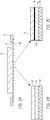
- FIG 2A is a schematic side view of a wafer 2' temporarily mounted to a wafer mount 11 by way of a wafer tape having a structural layer 12 and an insulating adhesive layer 4, according to various embodiments.
- the wafer 2' can comprise a semiconductor wafer that is patterned or formed to comprise a plurality of the integrated device dies, which may be similar to the dies 2 shown in Figures 1A-1B .
- the insulating adhesive layer 4 can be applied over the back side of the wafer 2', and the insulating layer 4 and structural layer 12 can couple the wafer 2' to the wafer mount 11.
- the wafer mount 11 can support the wafer 2' during processing. Examples of the wafer tape include Adwill LE tape manufactured by Lintec Corporation of Japan, and Dicing Die Attach Film manufactured by Henkel AG & Co. of Germany.
- Figure 2B is an enlarged schematic side view of a portion of the wafer 2' coupled with the structural layer 12 of the wafer tape by way of the insulating adhesive layer 4.
- the arrangement shown in Figure 2B can be the same as or similar to the package 1 shown in Figure 1A .
- utilizing the single insulating adhesive layer 4 to mount the die 2 to the carrier 3 may result in shorting of the bond wires 5 and the back side 7 of the die 2.
- Figure 2C is an enlarged schematic side view of a portion of the wafer 2' coupled with the wafer tape by way of a mounting structure 15, according to some embodiments.
- the mounting structure 15 can comprise a first layer 4 of a first insulating adhesive material and a second isolating film or layer 13 of insulating material between the first layer 4 and the wafer 2'.
- the second layer 13 can serve to electrically isolate at least a portion of the carrier 3 ( e.g ., the bond wires 5) from the back side 7 of the die 2.
- the second layer 13 can comprise a back side coat (BSC) layer that is deposited on the back side of the wafer 2', e.g ., by way of lamination, dispensing, screen printed, molded, etc.
- BSC back side coat
- the second layer 13 can comprise any suitable insulating material that is solid or hard enough such that the bond wires 5 do not penetrate the layer 13, and that electrically isolates the wires 5 from the die 2.
- the second layer 13 can comprise a polymer, e.g ., a thermoset polymer, a polyimide film or tape, etc.
- the second layer 13 may not have a flowable state, e.g ., the second layer 13 may comprise a solid material without causing the layer 13 to flow or melt during assembly or manufacturing.
- the second layer 13 can have a flowable state when it is applied to the wafer 2', but can be hardened such that the layer 13 is not flowable after mounting the wafer 2' to the wafer tape.
- the second layer 13 (which, as explained above, can serve as an electrically isolating layer for the package) can comprise a non-penetrating tape which can be applied to the back side 7 of the wafer 2', such as Adwill LC tape manufactured by Lintec Corporation of Japan.
- Figure 3A is a flow chart illustrate a method 29 for manufacturing an integrated device package, according to some embodiments.
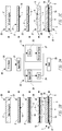
- Figure 3B illustrates a series of schematic side views of the package 1 at various stages of the method 29 shown in Figure 3A , according to one embodiment.
- Figure 3C illustrates a series of schematic side views of the package 1 at various stages of the method 29 shown in Figure 3A , according to another embodiment.
- the method 29 begins in a block 20, in which a wafer 2' having a plurality of integrated device regions is thinned from a back side of the wafer 2' to define the back sides 7 of the dies 2 once the wafer 2' is singulated or diced.
- the wafer 2' can be thinned in any suitable way, for example, by etching, polishing, etc.
- the second back side coat (BSC) or isolating layer 13 can be applied or deposited on the back side 7 of the wafer 2'.
- the second layer 13 can comprise a non-conductive or insulating material that is applied over the back side 7 of the wafer 2' in any suitable way.
- the second isolating layer 13 can be deposited, laminated, screen-printed, molded, or otherwise provided on the back side 7 of the wafer 2'.
- the method 29 moves to a block 22.
- the method 29 includes applying the first insulating adhesive layer 4 (e.g ., a die attach film, or DAF) over the second isolating layer 13 of the wafer 2'.
- the first layer 4 can be applied over the second layer 13 in any suitable manner, e.g ., deposited or screen printed onto the second isolating layer 13.
- the first insulating adhesive layer 4 can form part of the wafer tape (e.g ., the layer 4 may be attached to the structural layer 12 of the wafer tape).
- the wafer 2' can be mounted to the wafer tape, and the structural layer 12 can be removed to leave the insulating adhesive layer 4 attached to the isolating layer 13 on the back side 7 of the wafer 2'.
- the wafer 2' with layers 4, 13 can be diced, e.g ., sawed, punched, etc., to define a plurality of the integrated device dies 2.
- each diced die 2 can be stacked or mounted to the carrier 3.
- the diced die 2 can be brought together with the carrier 3, which can comprise another integrated device die in some embodiments.
- the carrier 3 can comprise a plurality of bond wires 5 configured to electrically connect bond pads on the front surface 8 of the carrier 3 to a packaging structure (such as a package substrate), which is not illustrated in Figure 3B .
- the package 1 can be heated ( e.g ., to a temperature in a range of 150 °C to 200 °C) to cause the first insulating layer 4 to change to the flowable state.
- the heating may not cause the second isolating layer 13 to melt or otherwise be flowable.
- the second layer 13 can have a higher melting point than the first layer 4 in some embodiments. In other embodiments, however, the second layer 13 may not have a higher melting point than the first layer 4.
- the second layer 13 may become a thermoset and may no longer melt. Accordingly, when the first layer 4 is heated and caused to flow, the second layer 13 may not be flowable but may remain solid.
- the first layer 4 can flow around the bonding wires 5 such that portions of the wires 5 are between the die 2 and the carrier 3 and such that the portions of the wires 5 are embedded in the first layer 4.
- the first layer 4 can comprise a sheet of insulating material (e.g., a DAF) applied over the second layer 13.
- the first layer 4 can change to the hardened or cured state to mount or stack the die 2 to the carrier 3.
- the first layer 4 may naturally harden or cure as it cools down.
- the first layer 4 can be baked to cause the layer 4 to harden or cure.
- the method 29 can move to a block 23 including a block 25.
- the wafer 2' with the second BSC isolating layer 13 can be diced to define a plurality of the integrated device dies 2, e.g., by sawing, punching, laser etching, plasma etching, or any other suitable manner.
- the first layer 4 can be dispensed on the front side 8 of the carrier 3.
- the first layer 4 can comprise a flowable epoxy paste or adhesive in the flowable state, and can be dispensed around and/or over the bond wires 5 in any suitable manner.
- the syringe can be heated and the dispensed epoxy material provided in any suitable pattern to control the flow and/or coverage of the epoxy.
- the epoxy or other flowable material can be dispensed between the wires, e.g ., in the middle portion of the die in the area inside or within the wire bond pads.
- the die 2 can be mounted to the carrier 3.
- the die 2 can be brought together against the first layer 4.
- the first layer 4 can harden ( e.g ., by cooling) to mount the die 2 to the carrier 3.
- the die 2 can contact the first layer 4 when the first layer 4 is in the flowable state so as to improve adhesion between the die 2 and the first layer 4.
- the first flowable layer 4 can be applied to the wafer 2' prior to dicing the wafer 2' into the plurality of dies 2.
- the wafer 2' can be diced after applying the second layer 13 and without applying the first layer 4 to the wafer 2'.
- the first layer 4 can be applied to the carrier 3 and flowed around the wires 5 ( e.g ., by way of an epoxy paste).
- the multi-layer mounting structure 15 can comprise a first sidewall 37 at a side surface of the first layer 4 and a second sidewall 36 at a side surface of the second layer 13.
- the first sidewall 37 can have a profile that is generally similar to the profile of the second sidewall 36, because both the first and second layers 4, 13 were diced in the block 26, which create markings indicative of the dicing procedure.
- some differences in the surfaces of the sidewalls 37, 36 may results due to the heating and cooling (and the resulting flowing and hardening) of the first layer 4.
- the sidewall 37 of the first layer 4 may have a curved profile (e.g., concave or convex) due to the flowing of the insulating material of the layer 4.
- the second sidewall 36 may be more planar or straighter than the first sidewall 37 (for example, due to the dicing operation).
- the first and second sidewalls 37, 36 may likewise differ.
- the second sidewall 36 can comprise markings representative of the dicing procedure and may be generally planar or straight.
- the first sidewall 37 can comprise a curved surface due to the flowable nature of the first layer 4.
- the thickness of the first layer 4 can be any suitable thickness sufficient to embed the wire bonds 5. In some embodiments, the thickness of the first layer 4 can be in a range of 25 microns to 100 microns.
- the thickness of the second isolating layer 13 can be any suitable thickness sufficient to prevent penetration of the layer 13 by the bond wires 5 and/or to prevent shorting to the integrated device die 2. In various embodiments, for example, the thickness of the second layer 13 can be in a range of 20 microns to 120 microns, in a range of 25 microns to 100 microns, in a range of 20 microns to 75 microns, in a range of 20 microns to 60 microns, or in a range of 25 microns to 50 microns. In some embodiments, the first layer 4 and the second isolating layer 13 may have different material compositions and an identifiable interface in the final product to indicate the application of multiple layers to form the structure 15.
- the embodiments of Figures 3A-3C can reduce the risk of, or can prevent, the shorting of the wires 5 and the integrated device die 2.
- the second layer 13 can physically and electrically isolate the wires 5 from the die 2.
- the wires 5 may be embedded in the first layer 4, the wires 5 may not penetrate the second layer 13 such that the wires 5 do not contact the back side 7 of the die 2.
- the second layer 13 can advantageously enable the use of increased voltages as compared with other packages ( e.g ., when higher voltage breakdown is desired).
- the second isolating layer 13 can reduce electromigration into the die 2.
- the layer 13 also provides a desired vertical separation distance or spacing between the die 2 and carrier 3.
- the isolating layer 13 may also be tuned in various embodiments to improve radio frequency (RF) performance of various types of systems.
- RF radio frequency
- the dielectric material of the layer 13 (and/or of other layers in the package) between the wires and the die 2 can be selected and/or dimensioned to improve system RF performance.
- the layer 13 (and/or other components) can be patterned or formed to target specific frequencies or wavelengths (or ranges thereof), for example, to act as a filter for attenuating, passing, or enhancing electromagnetic signals at those frequencies or wavelengths. Such embodiments can facilitate communications between the dies.
- various embodiments can improve inductive and/or capacitive performance of the package.
- the layers can be patterned to achieve the aforementioned advantages.
- microfluidic channels can be patterned in the layers (e.g ., including layer 13) so as to provide fluidic communication within the package.
- the layers (e.g ., layer 13) can also be patterned to provided locking features and/or to improve adhesion.
- a layer (such as the isolating layer 13) may be selected and/or dimensioned to have magnetic properties that can enhance performance, provide shielding capabilities, or other suitable functionality.
- the layer 13 can include an optical component to allow for communication between the die 2 and other components of the package or larger system.
- Figure 4A is a schematic side view of a wafer 2' temporarily mounted to a wafer mount 11 by way of a wafer tape 12, according to various embodiments.
- Figure 4B is an enlarged schematic side view of a portion of the wafer 2' coupled with the wafer 12 by way of a mounting structure 15, according to some embodiments.
- the components of Figures 4A-4B may be similar to or the same as like numbered components of Figures 2A and 2C , respectively.
- the undiced wafer 2' can comprise a plurality of device regions that, when diced, define a plurality of the integrated device dies.
- the mounting structure or tape 15 shown in Figure 4B can include at least three insulating layers that comprise an adhesive-insulator-adhesive stack.
- the mounting structure 15 can comprise a first insulating adhesive layer 4a that has a flowable state and a hardened or cured state (e.g ., a DAF or epoxy), and a second, solid isolating layer 13 disposed above the layer 4a between the wafer tape 12 and the wafer 2'.
- the second layer 13 can have a higher melting point than the first layer 4a, which may be similar to or the same material as the first layer 4 of Figure 2C .
- the second layer 13 may not have a higher melting point than the first layer 4a.
- the second layer 13 can comprise a thermoset material that hardens, and does not re-melt, after curing.
- the mounting structure or tape 15 can comprise a third insulating adhesive layer 4b over the second layer 13 and between the second layer 13 and the wafer 2' (and therefore between the second layer 13 and the die 2 after dicing as shown in Figure 5B ).
- the second layer 13 can be embedded or sandwiched between the first and third layers 4a, 4b.
- the third layer 4b can comprise the same material (or a generally similar material) as the first layer 4a.
- the third layer 4b can comprise a third insulating adhesive material that has a flowable state and a hardened or cured state.
- the first and third layers 4a, 4b may comprise different materials.
- providing the first and third layers 4a, 4b that have respective flowable states on opposite sides of the second layer 13 can enable adhesion to both, opposite sides of the structure or tape 15.
- heating the tape 15 of Figure 4B can cause the first and third layers 4a, 4b to flow, and the flowable layers 4a, 4b can contact a carrier and the die 2, respectively.
- the hardened layers 4a, 4b can beneficially improve the adhesion of the die 2' and the carrier to the structure 15.
- the tape 15 can be formed by applying or depositing the films or layers 4a, 4b on the opposite sides of the second insulating layer 13.
- the second layer 13 can be embedded within a flowable material (such as the first flowable layer 4 discussed above) and cut to define the first layer 4a on one side of the second layer 13 and the third layer 4b on the other side of the second layer 13.
- the first layer 4a, the second isolating layer 13, and the third layer 4b may have different material compositions and an identifiable interface in the final product to indicate the application of multiple layers to form the structure 15.
- the thickness of the tape 15 can be in a range of 70 microns to 300 microns, or in a range of 100 microns to 300 microns.
- the thickness of the first insulating adhesive layer 4a can be any suitable thickness, as explained above, for example in a range of 25 microns to 100 microns.
- the thickness of the third layer 4b can be in a range of 25 microns to 100 microns.
- the thickness of the second isolating layer 13 can be in a range of 20 microns to 120 microns, in a range of 25 microns to 100 microns, in a range of 20 microns to 75 microns, in a range of 20 microns to 60 microns, or in a range of 25 microns to 50 microns.
- the thickness of the second isolating layer 13 can be tuned according to various desired electrical characteristics, e.g ., the layer 13 can be made thicker for packages that operate at high voltages so that the thickness can be sufficient so as to avoid electrical breakdown.
- Figure 5A is a flowchart illustrating a method 14 for manufacturing an integrated device package 1, according to some embodiments.
- Figure 5B illustrates a series of schematic side views of the package 1 at various stages of the method 14 shown in Figure 5A , according to one embodiment.
- the method 14 can begin in a block 16 to thin the wafer 2'.
- the wafer 2' can be thinned by way of, for example, etching, polishing, etc.
- the mounting structure or tape 15 can be applied to the back side 7 of the wafer 2'.
- the multi-layered tape 15 can comprise the three layers 4a, 13, 4b described above in connection with Figures 4A-4B , such that the layers 4a, 13, 4b form a multi-layered structure that can be applied to the back side 7 of the entire (or portions of the) wafer 2'.
- the third layer 4b of the multi-layer tape 15 can be attached to the back side 7 of the wafer 2' in any suitable manner to connect the multi-layer mounting structure or tape 15 to the wafer 2'.
- the wafer 2' can be diced in any suitable way (e.g ., sawed, punched, etc.) to define a plurality of the integrated device dies 2.
- the diced die 2 can be stacked or mounted to the carrier 3 by way of the mounting structure or tape 15.
- the first layer 4a can be brought into contact with the bonding wires 5 of the carrier 3.
- the package 1 can be heated to cause the first layer 4A to flow around the bonding wires 5. Once the first layer 4a is cured or hardened, the die 2 can be securely adhered to the carrier 3.
- the second layer 13 can serve to electrically isolate the back side 7 of the die 2 from the carrier 3, e.g. , from the bonding wires 5.
- the use of the three layers 4a, 13, 4b in Figure 5B can beneficially improve adhesion of the die 2 to the multi-layer tape 15 (by way of the adhesion of the third layer 4b to the back side 7 of the die 2), and the adhesion of the multi-layer tape 15 to the carrier 3 (by way of the adhesion of the first layer 4a to the front side 8 of the carrier 3), while preventing or reducing the risk of shorts of the wires 5 to the die 2.
- Figure 6 illustrates four (4) example implementations of the embodiments of the multi-layer mounting structure or tape 15 disclosed herein.
- Example 1 illustrates the embodiments of the integrated device package 1 formed in the process shown in Figures 3B-3C .
- Example 2 illustrates the embodiment of the integrated device package 1 formed in the process shown in Figure 5B .
- the carrier 3 can comprise an additional integrated device die that is electrically connected to a package substrate (not shown) by bond wires 5.
- the carrier 3 can instead comprise a package substrate upon which the integrated device die 2 is mounted.
- the die 2 is mounted to the carrier 3 (package substrate) using the multi-layer mounting structure or tape 15 shown in Figures 3B-3C .
- the die 2 is mounted to the carrier 3 (package substrate) using the multi-layer mounting structure or tape 15 shown in Figure 5B .
- the carrier 3 can comprise a leadframe package substrate having a die pad and/or a plurality of leads. In other embodiments, however, the carrier 3 can comprise other types of package substrates or packaging structures, such as a PCB substrate, a ceramic substrate, etc.
- the embodiments of Examples 3 and 4 can securely adhere the die 2 to the carrier 3, and may reduce processing costs as compared with other processes that mount the die 2 to the package substrate (for example, may obviate the use of other, multi-step mounting processes).
- current processes may utilize multiple (e.g ., two) layers of a screen-printed epoxy paste for mounting the die 2 to the leadframe substrate. Screen-printing may incorporate multiple mechanical and thermal cycles, and may incur substantial processing costs. Utilizing the tape 15 in the devices of Examples 3 and 4 can reduce these manufacturing complexities and costs.
- Figure 7 is a schematic side sectional view of an integrated device package 1 in which the carrier 3 is mounted to a package substrate.
- the package substrate shown in Figure 7 comprises a leadframe substrate having a die pad 32 electrically spaced from a plurality of leads 34.
- the package 1 of Figure 7 illustrates the integrated device die 2 mounted to the carrier 3 (another integrated device die) by way of the multi-layer mounting structure 15 shown and described above in connection with Figures 3B and/or 3C.
- the die 2 can instead be mounted to the carrier 3 by way of the multi-layer mounting structure 15 shown and described in connection with Figure 5B .
- the carrier 3 can be mounted to the die pad 32 by way of a suitable die attach material 33.
- first bonding wires 5a can electrically connect the carrier 3 to the leads 34.
- Second bonding wires 5b can electrically connect the die 2 to the leads 34.
- the die 2 can be flip chip mounted to the carrier 3.
- a molding compound or encapsulant 31 can be provided over upper surfaces of the die pad 32 and leads 34, over the bonding wires 5a, 5b, and over the stacked die 2 and carrier 3.
- the leadframe substrate e.g ., the leads 34 and die pad 32
- Figures 8A-8B illustrate various packages 1 in which an integrated device die 2 is stacked or mounted to a carrier 3 that comprises another integrated device die. Unless otherwise noted, components of Figures 8A-8B may include the same or similar components as like-numbered components shown in Figures 1-7 .
- Figure 8A is a schematic side view of an integrated device package 1 in which the die 2 is mounted to the carrier 3 by only the intervening insulating adhesive layer 4. In Figure 8A , the lateral footprint of the die 2 is smaller than the lateral footprint of the carrier 3.
- Figure 8B is a schematic side view of an integrated device package 1 in which the die 2 is mounted to the carrier 3 by way of an intervening spacer 35, which may comprise silicon or any other suitable material.
- the spacer 35 can be attached to the carrier 3 by a die attach material 33, and the die 2 can be attached to the spacer 35 by a die attach material 33.
- Figures 8A-8B may experience various shortcomings as compared with various other embodiments disclosed herein.
- the bonding wires 5a may not be disposed between the die 2 and the carrier 3, such that there may be a line of sight or open gap between the wires 5a and the die 2. Such a line of sight may cause arcing between the wires 5a and the wires 5b, and/or between the wires 5a and the die 2.
- the die 2 may tilt during assembly and/or use, which can further increase the risk of arcing.
- a gap X may be provided between the spacer 35 and the bond wire 5a, but such an arrangement may nevertheless risk arcing or shorting if the die 2 tilts downwardly, and/or if there is bleedout of the die attach material 33.
- mounting the die 2 to the carrier 3 with the illustrated intervening structures may induce stresses on the carrier 3, and/or vice versa.
- attaching the spacer 35 to the carrier 3 may induce localized stresses in the carrier 3 (and/or in the die 2) around the perimeter of the spacer 35.
- stresses may also be induced in the package 1.
- an enacapsulant or molding compound is provided over the die 2 and carrier 3, these induced stresses may be effectively locked into the package 1.
- Figure 9A is a schematic side view of an integrated device package 1 comprising an integrated device die 2 mounted to a carrier 3 by way of a mounting structure 15 comprising a first insulating layer 4 and a second insulating element comprising a second spacer layer 35 between the first layer 4 and the die 2.
- Figure 9B is a schematic plan view of the integrated device package 1 shown in Figure 9A .
- the components of Figures 9A-9B are the same as or generally similar to like-numbered components of Figures 1A-8B .
- the carrier 3 (which can comprise an integrated device die) can be mounted to the die pad 32 of a leadframe substrate, for example, by way of the die attach material 33.
- One or more wire bonds 5a can be provided to electrically connect bond pads at the front side 8 of the carrier 3 with corresponding leads 34 of the leadframe substrate.
- the die 2 can be mounted or stacked to the carrier 3 by way of a mounting structure 15.
- the mounting structure 15 can comprise a first insulating adhesive layer 4 (which may be the same as or similar to the layers 4 and 4A described above) having a flowable state and a hardened or cured state.
- the mounting structure 15 can further comprise a second insulating element comprising a spacer 35 disposed between the die 2 and the first layer 4.
- the mounting structure 15 includes the spacer 35 and insulating layer 4, but in other embodiments, the mounting structure 15 can include the second isolating layer 13 and/or the third layer 4a described in Figures 3B-3C and 5B .
- the mounting structure 15 can be brought into contact with the bond wires 5a and can be changed into the flowable state (e.g., by heating the package 1).
- the first layer 4 can flow around and over the bond wires 5a.
- the first layer 4 can cure to securely attach the mounting structure 15 to the carrier 3.
- the mounting structure 15 can be formed by attaching or depositing the spacer 35 to the insulating adhesive layer 4, and the mounting structure 15 can subsequently be attached to the carrier 3.
- the insulating adhesive layer 4 can be attached to the carrier 3 (e.g ., flowed around the wire bonds 5 and cured), and the spacer 35 can be applied, deposited or attached to the insulating layer.
- Still other ways of forming the mounting structure 15 may be suitable.
- the integrated device die 2 can be mounted to the spacer 35 of the mounting structure by way of a die attach material 33. Bond pads at the front side 6 of the die 2 can be connected to corresponding leads 34 of the leadframe substrate.
- each layer may comprise any suitable thickness.
- the thickness of the first insulating layer 4 can be in a range of 25 microns to 100 microns.
- the thickness of the spacer 35 can be any suitable thickness for reducing stresses and/or for providing electrical isolation of the die, e.g., the thickness can be in a range of 100 microns to 200 microns.
- the thickness of the die attach material 33 that attaches the carrier 3 to the die attach pad 32 can be in a range of 15 microns to 75 microns, or any other suitable thickness.
- the thickness of the die attach material 33 that attaches the die 2 to the spacer 35 can be in a range of 15 microns to 75 microns, or any other suitable thickness.
- the embodiment shown in Figures 9A-9B may prevent or reduce the risk of shorting the bond wires 5 to the die 2, as explained above.
- the spacer 35 may comprise a material that prevents penetration of the bond wires 5.
- the material of the spacer may be selected so as to closely match a coefficient of thermal expansion (CTE) of the die 2 and/or the carrier 3.
- CTE of the spacer 35 can be within at least +/- 50% of the CTE of the integrated device die 2, within at least +/- 75% of the CTE of the integrated device die 2, within at least +/- 90% of the CTE of the integrated device die 2, or within at least +/- 95% of the CTE of the integrated device die 2.
- the CTE of the spacer 35 can be substantially the same as the CTE of the die 2.
- the CTE of the spacer can be within at least +/- 50% of the CTE of the carrier 3, within at least +/- 75% of the CTE of the carrier 3, within at least +/- 90% of the CTE of the carrier 3, or within at least +/- 95% of the CTE of the carrier 3.
- the CTE of the spacer 35 can be substantially the same as the CTE of the carrier 3.
- matching the CTE of the spacer 35 with the CTE of the carrier 3 and/or die 2 can reduce overall stresses in the package 1.
- the spacer 35 can spread any stresses induced by the die 2 over a larger area, reducing local stress concentrations, such as those created around the perimeter of the spacer 35 shown in Figure 8B .
- the spacer 35 can comprise any suitable material, including, for example, a semiconductor ( e.g ., silicon), a polymer, etc.
- the spacer 35 can comprise a tunable structure, e.g ., a bimetallic strip which can be tuned to achieve a desired CTE.
- the spacer 35 can be tuned to have a desired, predetermined CTE mismatch to induce a particular stress for a particular electrical reaction and/or behavior.
- multiple integrated device dies 2a, 2b (which may comprise the same or different type of integrated device die) can be mounted laterally side-by-side on the spacer 35.
- including multiple dies 2a, 2b on the spacer 35 may improve redundancy for the package 1, for example, if the dies 2a, 2b perform at least some overlapping functions.
- the spacer 35 can create the same stress conditions for the dies 2a, 2b, which may improve the electrical performance of the dies 2a, 2b.
- multiple spacers 35 may be provided.
- multiple dies 2A, 2B, etc. can be mounted to corresponding multiple spacers.
- more than two integrated device dies may be mounted on the spacer 35.
- Figures 10A-13 illustrate embodiments that incorporate a multi-layer mounting structure that comprises the first insulating layer and the spacer 35.
- Figure 10A is a side view of a package 1 in which the integrated device die 2 can be approximately the same lateral size or footprint (in at least one horizontal dimension) as the spacer 35.
- the spacer 35 in Figure 10A may be approximately the same lateral size or footprint (in at least one horizontal dimension) as the carrier 3.
- Figure 10B is a side view of a package 1 that includes two integrated device dies 2, 2' and a carrier 3 (which may also comprise an additional, third integrated device die).
- the integrated device die 2 can be mounted to the carrier 3 by way of the adhesive 4, the spacer 35, and the die attach material 33.
- a second integrated device die 2' can be mounted to the integrated device die 2 by way of a second adhesive 4', a second spacer 35', and a second die attach material 33'.
- the lateral size of the integrated device dies 2, 2' can be the same as the lateral size of the spacer 35.
- the carrier 3 illustrated in Figure 10B can be connected to the die pad 32 via conductive bumps 38.
- the integrated device dies 2, 2' can be wire bonded to the leads 34 by way of bonding wires 5b, 5b'.
- the integrated device die 2 may have a lateral size or footprint that is smaller than the lateral size or footprint of the spacer 35 and/or the carrier 3.
- the spacer 35 may have a lateral size or footprint in at least one lateral dimension that is approximately the same as the lateral size of the carrier 3.
- the integrated device die 2 may have a lateral size or footprint that is smaller than the lateral size or footprint of the spacer 35.
- the lateral size or footprint of the spacer 35 may be smaller than the lateral size or footprint of the carrier 3.
- the integrated device die 2 may have a lateral size or footprint that is larger than the lateral size or footprint of the spacer 35 and/or the carrier 3.
- the spacer 35 is illustrated as being about the same lateral size or footprint as the carrier 3, but in other embodiments, the spacer 35 may have a smaller lateral size than the carrier 3.
- Still other combinations of lateral size and/or footprint of the die 2, the spacer 35, and the carrier 3 may be suitable for the embodiments disclosed herein.
- each of the embodiments of Figures 10A-13 may reduce the risk of electrical shorting or arcing and reduce the overall stresses of the package 1.
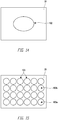
- Figure 14 is a schematic top view of a spacer 35 according to an embodiment.
- the spacer 35 of Figure 14 may be implemented in any of the packages 1 disclosed herein.
- the spacer 35 illustrated in Figure 14 includes an opening 102.
- the opening 102 can enable the use of functionality for other integrated circuit and/or packaging applications.
- the opening 102 may be pattered or formed as desired for the specific application.
- the opening 102 may comprise a hole through a portion of the spacer 25 as illustrated in Figure 14 , or comprise a cavity formed partially through a portion of the spacer 25.
- an insert e.g., an optical insert such as a lens or a filter
- the insert may enable optical communication through the spacer 35 between the die 2 and the carrier 3, or between other stacked components between which the spacer 35 is disposed.
- Figure 15 is a schematic top view of a spacer 35 according to another embodiment.
- the spacer 35 of Figure 15 may be implemented in any of the packages 1 disclosed herein.
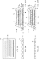
- the spacer 35 illustrated in Figure 15 includes a plurality of openings 103.
- the openings 103 may be filled with a filler material or inserts (e.g., lens or filters).
- the openings 103 can be vertically integrated in the system so as to provide optical or electrical communication between the die 2 and the carrier 3.
- the filler material can be, for example, an epoxy, such as SU-8.
- the spacer 35 can be modified by, for example, using a laser to modify the property of the filler material.
- SU-8 filler material can be modified to allow/prohibit light to pass therethrough.
- openings 103 there are twenty-four (24) openings 103 equally spaced from one another in Figure 15 .
- the spacer 35 may comprise any number of openings 103 with suitable spacings between the openings 103.
- the openings 103 may have any suitable shape and/or size.
- different openings 103a, 103b of the openings 103 can include different filler materials and/or inserts.
- one or more first openings 103a can include a first type of filler material or insert
- one or more second openings 103b can include a second type of filler material or insert.
- the use of different filler materials or inserts in different regions of the spacer 35 can enable different functionalities across the spacer 35.
- Different materials/inserts can be incorporated within the same space, enabling (for example) light of different wavelengths to transmit through different portions of the same spacer/substrate - therefore though the different planes of the vertically integrated structure linking up different components within the system.
- Figure 16 is a schematic top view of a spacer 35 according to another embodiment.
- the spacer 35 of Figure 16 may be implemented with any of the packages 1 disclosed herein.
- the spacer 35 illustrated in Figure 16 includes a pattern of material 104.
- the patterned material 104 may be dispensed on and/or embedded into the spacer 35.
- the pattern of material 104 can comprise a metallic pattern, conductive pattern, insulator pattern, etc.
- the patterned material 104 can comprise a spiral or curved pattern.
- the patterned material 104 may be beneficial for use with magnetic sensor or magnetic switch applications.
- the patterned material 104 may be used as a band pass filter.
- the patterned material 104 may be used in conjunction with packages that harvest energy by, for example, harnessing vibration, light, and/or heat to collect and store energy for other uses.
- Figure 17 is a schematic top view of a spacer 35 according to another embodiment.
- the spacer 35 of Figure 17 may be implemented with any of the packages 1 disclosed herein.
- the spacer 35 illustrated in Figure 17 includes an optical filter 105 formed through at least a portion of a thickness of the spacer 35.
- the filter 105 may be disposed on or into the thickness of the spacer 35, and can be configured to pass or attenuate light at selected optical frequency ranges.
- the spacer 35 illustrated in Figure 17 may be beneficial for use with biomedical applications and/or optical applications, in some embodiments.
- the filter 105 may comprise a wavelength filter, band pass filter, etc.
- Figure 18 is a schematic top view of a spacer 35 according to another embodiment.
- the spacer 35 of Figure 18 may be implemented with any of the packages 1 disclosed herein.
- the spacer 35 illustrated in Figure 18 can be used in fluidic applications, and can includes a fluid pathway 106 patterned or otherwise defined in the spacer 35.
- the fluid pathway 106 may be disposed on or into the spacer 35.
- the fluid pathway 106 can comprise a channel, a via, a track, a microfluidic channel, etc. for conveying fluid through the spacer 35. Fluid can be driven through the fluid pathway 106 along a lateral direction of the spacer 35 (as shown in Figure 18 ) or vertically through the spacer 35.
- the spacer 35 can also include a valve 107 along the fluid pathway 106.
- the valve 107 can be configured to control a flowrate of fluid along the fluid pathway 106.
- the valve 107 can comprise a piezoelectric material.
- the spacer 35 with the fluid pathway 106 may be used in various types of fluidic applications, including, e.g ., a pH sensor, a blood sensor, medical fluids therapy, pharmaceutical tests and devices, food industry tests and devices, polymeric chain reaction (PCR) devices, etc.
- the fluid pathway 106 may be suitably patterned for the desired application.
- the valve 107 may not be incorporated in the spacer 35.
- fluid may flow through the spacer 35 and/or between the spacer 35 and an adjacent layer in the package, without being controlled by the valve 107.
- the fluid pathway 106 e.g., a microfluidic channel
- the fluid pathway 106 can interact with the fluid flowing through the spacer and other layers, in some embodiments.
- one of the layers in a package may monitor the temperature of the fluid and/or extrapolate some other property of the fluid (e.g., magnetic structures detecting some magnetic property, flow rate, and/or an optical property of the fluid).
- the valve 107 can include an optical component (e.g., an optical sensor) to detect an optical property of the fluid.
- FIG 19 is a schematic top view of a spacer 35 according to another embodiment.
- the spacer 35 of Figure 19 may be implemented with any of the packages 1 disclosed herein.
- the spacer 35 illustrated in Figure 19 includes a sensor 108.
- the sensor 108 may be disposed on or into the spacer 35.
- the sensor 108 can comprise a radio frequency identification (RFID) device.
- RFID radio frequency identification
- the sensor 108 may enable a wireless communication between the package 1 and an external device, or between device dies within the package 1.
- the sensor 108 may enable the package for use with an internet of things (IoT) system by wirelessly receiving and/or transmitting information to external devices.
- the sensor 108 may also provide data encryption capabilities for the package 1.
- IoT internet of things
- Figure 20 is a schematic top view of a spacer 35 according to another embodiment.
- the spacer 35 of Figure 20 may be implemented with any of the packages 1 disclosed herein.
- the spacer 35 illustrated in Figure 20 includes a patterned void 109.
- the patterned void 109 may be formed on or into the spacer 35.
- the void 109 may comprise, for example, a trench 110 or a channel 111 as illustrated in Figures 21A and 22A , respectively.
- the spacer 35 with the patterned profile can be beneficial for use a band pass filter, which can filter light of various wavelengths.
- the spacer 35 can comprise silicon, polymer, or any suitable material.
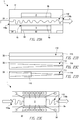
- Figure 21A is a side view of the spacer 35 that includes a plurality of trenches 110 according to an embodiment.
- the spacer 35 of Figure 21A may be implemented with any of the packages 1 disclosed herein.
- the trenches 110 may be formed ( e.g ., etched) into a portion of a thickness of the spacer 35.
- the trenches 110 may be suitably spaced from one another, for example, to provide optical filtering functionality at desired wavelength ranges.
- the trenches 110 may be configured to enable media to traverse laterally and/or vertically through layers of a package.
- the spacer 35 and/or any layer(s) of the package can be connected to an external system and/or component. For example, a specific layer of the package can communicate with an external optical network or the fluid to be analyzed and/or modified can ingress from, for example, the external environment.
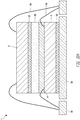
- Figure 21B is a schematic side sectional view of an integrated device package 1 that includes the spacer 35 of Figure 21A .
- the carrier 3 of package 1 is mounted to a package substrate.
- the package 1 of Figure 21B comprises a leadframe substrate having a die pad 32 electrically spaced from a plurality of leads 34.
- the package 1 of Figure 21B illustrates a integrated device die 2 mounted to a carrier 3 (another integrated device die) by way of a multi-layer mounting structure 15 that comprises the spacer 35.
- the multi-layer mounting structure 15 illustrated in Figure 21B includes a first insulating adhesive layer 4a between the carrier 3 and the spacer 35, and a third insulating adhesive layer 4b between the die 2 and the spacer 35.
- the die 2 can instead be mounted to the carrier 3 by way of the multi-layer mounting structure 15 that comprises any number of insulating adhesion layer(s).
- the carrier 3 can be mounted to the die pad 32 by way of a suitable die attach material 33.
- first bonding wires 5a can electrically connect the carrier 3 to the leads 34.
- Second bonding wires 5b can electrically connect the die 2 to the leads 34.
- the die 2 can be flip chip mounted to the carrier 3.
- a molding compound or encapsulant for example, the encapsulant 31 of Figure 7
- the leadframe substrate e.g ., the leads 34 and die pad 32
- the leadframe substrate e.g ., the leads 34 and die pad 32
- the leadframe substrate e.g ., the leads 34 and die pad 32
- the leadframe substrate e.g ., the leads 34 and die pad 32
- Figure 22A is a side view of the spacer 35 that includes a plurality of channels 111 according to an embodiment.
- the spacer 35 of Figure 22A may be implemented with any of the packages 1 disclosed herein.
- the channels 111 can comprise channels disposed laterally through the spacer 35, e.g., parallel to major surfaces of the spacer 35.
- the channels 111 can comprise discrete voids or spaces within the spacer 35.
- the size and spacing of the channels 111 can be selected to provide optical filtering or other suitable types of functionality.
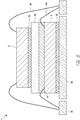
- Figure 22B is a schematic side sectional view of an integrated device package 1 that includes the spacer 35 of Figure 22A .
- the carrier 3 of package 1 is mounted to a package substrate.
- the package 1 of Figure 22B comprises a leadframe substrate having a die pad 32 electrically spaced from a plurality of leads 34.
- the package 1 of Figure 22B illustrates an integrated device die 2 mounted to a carrier 3 (another integrated device die) by way of a multi-layer mounting structure 15 that comprises the spacer 35.
- the multi-layer mounting structure 15 illustrated in Figure 22B includes a first insulating adhesive layer 4a between the carrier 3 and the spacer 35, and a third insulating adhesive layer 4b between the die 2 and the spacer 35.
- the die 2 can instead be mounted to the carrier 3 by way of the multi-layer mounting structure 15 that comprises any number of insulating adhesion layer(s).
- the carrier 3 can be mounted to the die pad 32 by way of a suitable die attach material 33.
- first bonding wires 5a can electrically connect the carrier 3 to the leads 34.
- Second bonding wires 5b can electrically connect the die 2 to the leads 34.
- the die 2 can be flip chip mounted to the carrier 3.
- a molding compound or encapsulant for example, the encapsulant 31 of Figure 7
- the leadframe substrate e.g ., the leads 34 and die pad 32
- the leadframe substrate e.g ., the leads 34 and die pad 32
- the leadframe substrate e.g ., the leads 34 and die pad 32
- the leadframe substrate e.g ., the leads 34 and die pad 32
- the channels 111 may be constructed to enable fluid and/or optical signals to travel along the spacer 35, in some embodiments.
- the trenches 111 may be configured to enable media to traverse laterally and/or vertically through layers of the package 1.
- the spacer 35 and/or any layer(s) of the package 1 can be connected to an external system and/or component.
- a specific layer of the package 1 can communicate with an external optical network.
- a microfluidic channel that is included in the package 1 e.g., within the stacked module/vertically integrated system
- Figure 23A is a schematic side sectional view of an integrated device package 1 according to another embodiment.
- the carrier 3 of the package 1 is mounted to a package substrate.
- the package 1 of Figure 23A comprises a leadframe substrate having a die pad 32 electrically spaced from a plurality of leads 34.
- the package substrate can comprise a laminate substrate.
- the package 1 of Figure 23A illustrates a integrated device die 2 mounted to a carrier 3 (another integrated device die) by way of a multi-layer mounting structure 15 that comprises the spacer 35.
- the multi-layer mounting structure 15 illustrated in Figure 23A includes a first insulating adhesive layer 4a between the carrier 3 and the spacer 35, and a third insulating adhesive layer 4b between the die 2 and the spacer 35.
- the die 2 can instead be mounted to the carrier 3 by way of the multi-layer mounting structure 15 that comprises any number of insulating adhesion layer(s).
- the spacer 35 illustrated in Figure 23A includes a pathway 112 disposed laterally along or within the spacer 35.
- the pathway 112 can comprise any suitable type of pathway, such as a fluidic pathway, a microfluidic pathway, an optical pathway, or an electronic pathway.
- the pathway 112 can accordingly provide fluid, optical, and/or electronic communication along a lateral direction parallel to and between the die 2 and the carrier 3, for example, between input terminal 116a and output terminal 116b.
- the pathway 112 can comprise a fluid piping tube or channel.
- the carrier 3 can be mounted to the die pad 32 by way of a suitable die attach material 33.
- a molding compound or encapsulant 31 can be provided over upper surfaces of the die pad 32 and leads 34, over the stacked die 2 and carrier 3, and over upper and lower surfaces of the spacer 35.
- the spacer 35 can be disposed between portions of the encapsulant 31.
- the leadframe substrate e.g ., the leads 34 and die pad 32
- FIG 23A does not illustrate bonding wires, it should be appreciated that, as explained above, bonding wires can be provided within the layer 4a to connect the carrier 3 to the leads 34.
- the spacer 35 can serve to isolate the bonding wires from other components of the package 1.
- the pathway 112 (e.g., a microfluidic channel) can be used to remove heat from the package 1, in some embodiments.
- the pathway 116 can interact with the fluid flowing through the spacer and other layers, in some embodiments.
- one of the layers in a package e.g., a layer integrated above or below the spacer 35
- can monitor the temperature of the fluid and/or extrapolate some other property of the fluid e.g., magnetic structures detecting some magnetic property, flow rate, an optical property of the fluid flowing through etc.
- Figures 23B-23D illustrate schematic side sectional views of various embodiments of a spacer 35 having a pathway 112.
- the spacer 35 illustrated in Figure 23B includes a pathway 112 that comprises a fiber optic channel 113.
- the pathway 112 of the spacer 35 can be used to enable optical communication laterally through the spacer 35 along the fiber optic channel 113.
- the spacer 35 illustrated in Figure 23C includes a pathway 112 having a tapered channel 114, which may be used with fluidic applications, for example.
- fluid can be driven through the tapered channel 114 laterally along the spacer 35.
- the spacer 35 illustrated in Figure 23D includes the tapered channel 114 with fluidic device 115 (e.g ., a filter or pump) disposed in or along the tapered channel 114.
- the fluidic device 115 can interact with the fluid to filter materials from the fluid or to drive the liquid through the pathway 112.
- the spacer 35 can connect to external networks or devices by way of the terminals 16a, 16b to provide optical, electrical, or fluidic communication with those external networks or devices.
- Figure 23E illustrates a schematic top view of the package 1 of Figure 23A .
- first bonding wires 5a can electrically connect the carrier 3 to the leads 34.
- Second bonding wires 5b can electrically connect the die 2 to the leads 34.
- the die 2 can be flip chip mounted to the carrier 3.
- the spacer 35 can be provided over the bonding wires so as to prevent shorting.
- Figure 24 is a schematic side sectional view of an integrated device package 1 that includes two integrated device dies 2, 2', and a carrier 3 stacked vertically.
- the carrier 3 is mounted to a die pad 32 by way of an adhesive 33, and the carrier 3 is electrically connected to leads 34 by way of bonding wires 5a.
- a multi-layer mounting structure 15 includes a spacer 35a, a first insulating adhesive layer 4a between the carrier 3 and the spacer 35a, and a third insulating adhesive layer 4b between the die 2 and the spacer 35a.
- the spacer 35a illustrated in Figure 24 can be the same or generally similar to the spacer 35 illustrated in Figure 22A .
- lateral channels 111 can be provided through the spacer 35a.
- the channels 111 can provide optical, electrical, or fluidic pathways through the spacer 35a.
- the two integrated device dies 2, 2' are spaced from one another by a spacer 35b that includes a plurality of openings 103.
- the spacer 35b illustrated in Figure 24 can be the same or generally similar to the spacer 35 illustrated in Figure 15 .
- the openings 103 can be filled or unfilled with a filler material.
- the openings 103 can comprise vertical vias, optical pathways, etc.
- the two dies 2, 2' can electrically, optically, and/or fluidly communicate through the openings 103.
- the integrated device die 2 illustrated in Figure 24 is electrically connected to the leads 34 by way of bonding wires 5b.
- a spacer 35c that can be the same or generally similar to the spacer 35 illustrated in Figure 14 is disposed over the integrated device die 2'.
- the spacer 35c can include an opening 102.
- the opening can be filled or unfilled with a filling material.
- the opening 102 can comprise a via, an optical path, etc.
- the opening 102 can be larger than the opening 103, in some embodiments.
- a molding compound or encapsulant 31 can be provided about the stacked spacers 35a-35c, dies 2, 2', and carrier 3.
- the encapsulant 31 can have an opening 120 over the opening 102 of the spacer 35c. In some embodiments, there may be no encapsulant 31 over the spacer 35c. In certain applications, the opening 120 and the opening 102 can allow the integrated device die 2' to communicate with outside environs and/or another device, for example, optically and/or fluidly.
- the integrated device package 1 illustrated in Figure 24 may be suitable for fiber optic communications.
- the spacers 35a, 35b, 35c can comprise any other suitable structures, such as those illustrated in Figures 14-20 , for the use of the integrated device package 1.
- Figure 25A illustrates a schematic side sectional view of a laminate substrate 122.
- the laminate substrate 122 includes a plurality of alternating patterned conductive and non-conductive layers.
- the laminate substrate 122 can comprise a printed circuit board (PCB) substrate.
- the laminate substrate 122 can include various electronic components therein.
- the laminate substrate 122 can include vias, lens, filters, modified areas, voids, cavities, etc.
- Figure 25A shows interconnection terminals 124a, 124b (such as fluid and/or fiber optic connections) coupled to openings 126a, 126b.
- a terminal 124a, 124b and/or an opening 126a, 126b may be provided to any spacer disclosed herein.
- the laminate substrate can communicate (e.g., receive an input or transmit an output), for example, electrically, fluidly, and/or optically, with the outside environment and/or an external system or a device.
- Figure 25B illustrates a schematic side sectional view of the laminate substrate 122 that is mounted on a carrier 128.
- the carrier 128 has a top side or a back side 128a and a bottom side or a front side 128b.
- the front side can comprise an active surface.
- the carrier 128 can include vias 130 extending from the back side 128b to the front side 128b.
- the front side 128b of the carrier can have solder balls 132 to provide electrical communication between the vias 130 and an external device.
- the laminate substrate 122 and the carrier 128 can be in electrical connection.
- the carrier 128 can comprise an application specific integrated circuit (ASIC) with through substrate vias TSVs.
- ASIC application specific integrated circuit
- active circuitry of the ASIC can control or manage functions of the laminate substrate 122.
- FIG 25C illustrate a schematic side sectional view of an integrated device package 1 that includes the laminate substrate 122 and the carrier 128 of Figure 25B , according to an embodiment.
- the integrated device package 1 has a generally similar structure as the integrated device package 1 illustrated in Figure 10A except that the package 1 of Figure 25C includes the laminate substrate 122 and the carrier 128 and a molding compound or encapsulant 31.
- the solder balls 132 of the carrier 128 can electrically connect to corresponding contact pads on the die 2.
- the carrier laminate substrate 122 can be exposed through, and positioned above, the encapsulant 31. Additional devices or dies (not shown) can electrically connect to the top surface of the substrate 122.
- Figure 25D illustrate a schematic side sectional view of an integrated device package 1 that includes the laminate substrate 122 and the carrier 128 of Figure 25B , according to an embodiment.
- the package 1 illustrated in Figure 25D is generally similar to the package 1 illustrated in Figure 25C except that the encapsulant 31 in Figure 25D covers side walls of the laminate substrate 122.
Landscapes
- Engineering & Computer Science (AREA)
- Microelectronics & Electronic Packaging (AREA)
- Computer Hardware Design (AREA)
- Die Bonding (AREA)
- Structures Or Materials For Encapsulating Or Coating Semiconductor Devices Or Solid State Devices (AREA)
- Manufacturing & Machinery (AREA)
- Wire Bonding (AREA)
Abstract
Description
- This application claims priority to
U.S. Provisional Patent Application No. 62/656,840 - The field relates to mounting structures (e.g., mounting films or tapes) for integrated device packages.
- Various types of integrated device packages include an integrated device die mounted to a carrier, which may comprise a second integrated device die. Stacking the integrated device die on the carrier may introduce stresses on the carrier, or vice versa. Furthermore, in some packages, the carrier (e.g., an integrated device die) can be wire bonded to another structure, such as a package substrate. In such packages, it can be challenging to provide adequate electrical isolation between portions of the carrier and portions of the integrated device die. Furthermore, stacking the integrated device die on the carrier may induce stresses in the carrier and/or in the die. Accordingly, there remains a continuing need for improved integrated device packages that include a die stacked or mounted on a carrier.
- In one aspect, an integrated device package is disclosed. The integrated device package (or "package") can comprise a carrier and an integrated device die having a front side and a back side. A mounting structure can serve to mount the back side of the integrated device die to the carrier. The mounting structure can comprise a first adhesive layer over the carrier and a second element between the back side of the integrated device die and the first adhesive layer. The first adhesive layer can comprise a first insulating material that adheres to the carrier. The second element can comprise a second insulating material that electrically separates the integrated device die from the carrier and/or from an electrical interconnect connected to the carrier.
- In one embodiment, the first insulating material has a first flowable state and a second hardened state.
- In one embodiment, the carrier comprises a package substrate. The package substrate can comprise a leadframe substrate or a laminate substrate.
- In one embodiment, the first layer comprises a die attach film (DAF) or an epoxy paste. The first layer can comprises an epoxy paste.
- In one embodiment, the second element comprises a solid coating that is applied over the back side of the integrated device die.
- In one embodiment, the second element comprises a spacer that is attached to the first layer. The spacer can include a pathway to provide at least one of electrical, optical, and fluidic communication between an input terminal and an output terminal of the spacer. The pathway can extend vertically through the spacer to provide communication between the carrier and the integrated device die. The pathway can include a fiber optic channel. The integrated device package can further include a second spacer over the integrated device die. The second spacer can include a second pathway. The second pathway can provide communication between the integrated device die and the outside environs.
- In one embodiment, a coefficient of thermal expansion (CTE) of the spacer is within at least +/-90% of one or more of a coefficient of expansion of the integrated device die and a coefficient of thermal expansion of the carrier.
- In one embodiment, a first exposed sidewall of the first layer defines a first profile, and second exposed sidewall of the second element defines a second profile. The first profile comprises a curved or non-linear surface and the second profile comprises a generally planar surface.
- In one embodiment, the mounting structure comprises a third layer between the back side of the integrated device die and the second element such that the second element is embedded between the first layer and the third layer. The third layer can comprise a third insulating material.
- In one embodiment, one or both of the first layer and the second element comprises a polymer.
- In one embodiment, the integrated device die is laterally smaller than the mounting structure.
- In one aspect, multi-layer mounting tape for attaching an integrated device die to a carrier and electrically isolating a back side of the integrated device die from the carrier is disclosed. The multi-layer mounting tape can comprise a first layer comprising a first insulating material having a first flowable state and a second hardened state. The multi-layer mounting tape can comprise a second layer over the first layer, the second layer comprising a second insulating material. The multi-layer mounting tape can comprise a third layer over the second layer, such that the second layer is embedded between the first layer and the third layer, the third layer comprising a third insulating material, the third insulating material having a first flowable state and a second hardened state.
- In one embodiment, the first and third layers each comprise a die attach film (DAF).
- In one embodiment, the second layer comprises a thermoset polymer.
- In one aspect, a method of manufacturing an integrated device package is disclosed. The method can include mounting a back side of an integrated device die to a carrier by way of a multi-layer mounting structure, the multi-layer mounting structure comprising a first layer over the carrier and a second element over the first layer. The first layer can comprise a first insulating material that adheres to the carrier. The second element can comprise a second insulating material that electrically separates the integrated device die from the carrier and/or from an electrical interconnect connected to the carrier.
- In one embodiment, the second element comprises a second layer. The method can further include applying the second layer to the back side of a wafer that comprises a plurality of device regions. After the applying, dicing the wafer into a plurality of integrated device dies. The plurality of integrated device dies comprises the integrated device die.
- In one embodiment, the method further includes before the mounting, applying the first layer to a bottom surface of the second layer.
- In one embodiment, the method further includes, before the mounting, applying the first layer to a top surface of the carrier.
- In one embodiment, the carrier comprises a second integrated device die wire bonded to a package substrate by a bonding wire. The method further includes bringing together the integrated device die and the carrier with the multi-layer mounting structure between the integrated device die and the carrier, and causing the first layer in the first flowable state to flow around the bonding wire.
- In one aspect, an integrated device package is disclosed. The integrated device package can include a carrier. The integrated device package can also include an integrated device die that has a front side and a back side. The integrated device package can further include a mounting structure that serves to mount the back side of the integrated device die to the carrier. The mounting structure includes a first adhesive layer over the carrier and a spacer between the back side of the integrated device die and the first adhesive layer. The spacer includes a pathway to provide at least one of electrical, optical, and fluidic communication between an input terminal and an output terminal of the spacer.
- In one embodiment, the pathway extends vertically through the spacer to provide communication between the carrier and the integrated device die.
- In one embodiment, the pathway comprises a fiber optic channel.
- In one embodiment, the integrated device package further includes a second spacer over the integrated device die, the second spacer includes a second pathway, the second pathway providing communication between the integrated device die and the outside environs.
- Details of one or more implementations of the subject matter described in this specification are set forth in the accompanying drawings and the description below. Other features, aspects, and advantages will become apparent from the description, the drawings, and the claims. Note that the relative dimensions of the following figures may not be drawn to scale.
- Non-limiting aspects of the disclosure are set out in the following numbered clauses.
- 1. An integrated device package comprising:
- a carrier;
- an integrated device die having a front side and a back side; and
- a mounting structure that serves to mount the back side of the integrated device die to the carrier, the mounting structure comprising a first adhesive layer over the carrier and a second element between the back side of the integrated device die and the first adhesive layer,
- wherein the first adhesive layer comprises a first insulating material that adheres to the carrier,
- wherein the second element comprises a second insulating material that electrically separates the integrated device die from an electrical interconnect connected to the carrier.
- 2. The integrated device package of
Clause 1, wherein the carrier comprises a second integrated device die. - 3. The integrated device package of
Clause 2, wherein the electrical interconnect comprises a bonding wire, the integrated device package further comprising a package substrate, the second integrated device die wire bonded to the package substrate by the bonding wire, wherein a portion of the bonding wire is disposed between the second element and the second integrated device die, the portion of the bonding wire being embedded within the first layer. - 4. The integrated device package of
Clause 3, wherein the bonding wire does not protrude into the second element, and the second element physically and electrically isolates the bonding wire from the back side of the integrated device die. - 5. The integrated device package of
Clause 3 orClause 4, wherein the integrated device die is wire bonded to the package substrate. - 6. The integrated device package of any preceding Clause, wherein the first insulating material has a first flowable state and a second hardened state.
- 7. The integrated device package of any preceding Clause, wherein the carrier comprises a package substrate.
- 8. The integrated device package of
Clause 6, wherein the package substrate comprises a leadframe substrate or a laminate substrate. - 9. The integrated device package of any preceding Clause, wherein the first layer comprises a die attach film (DAF) or an epoxy paste.
- 10. The integrated device package of any preceding Clause, wherein the first layer comprises an epoxy paste.
- 11. The integrated device package of any preceding Clause, wherein the second element comprises a solid coating applied over the back side of the integrated device die.
- 12. The integrated device package of any preceding Clause, wherein the second element comprises a spacer attached to the first layer.
- 13. The integrated device package of
Clause 7, wherein the spacer comprises a pathway to provide at least one of electrical, optical, and fluidic communication between an input terminal and an output terminal of the spacer. - 14. The integrated device package of
Clause 8, wherein the pathway extends vertically through the spacer to provide communication between the carrier and the integrated device die. - 15. The integrated device package of
Clause 8 orClause 14, wherein the pathway comprises a fiber optic channel. - 16. The integrated device package of any of
Clauses 8 to 15, further comprising a second spacer over the integrated device die, the second spacer includes a second pathway, the second pathway providing communication between the integrated device die and the outside environs. - 17. The integrated device package of any of
Clauses 7 to 16, wherein a coefficient of thermal expansion (CTE) of the spacer is within at least +/-90% of one or more of a coefficient of expansion of the integrated device die and a coefficient of thermal expansion of the carrier. - 18. The integrated device package of any preceding Clause, wherein a first exposed sidewall of the first layer defines a first profile and wherein a second exposed sidewall of the second element defines a second profile, wherein the first profile comprises a curved or non-linear surface and the second profile comprises a generally planar surface.
- 19. The integrated device package of any preceding Clause, wherein the mounting structure comprises a third layer between the back side of the integrated device die and the second element such that the second element is embedded between the first layer and the third layer, the third layer comprising a third insulating material.
- 20. The integrated device package of any preceding Clause, wherein one or both of the first layer and the second element comprises a polymer.
- 21. The integrated device package of any preceding Clause, wherein the integrated device die is laterally smaller than the mounting structure.
- 22. A multi-layer mounting tape for attaching an integrated device die to a carrier and electrically isolating a back side of the integrated device die from the carrier, the multi-layer mounting tape comprising:
- a first layer comprising a first insulating material having a first flowable state and a second hardened state;
- a second layer over the first layer, the second layer comprising a second insulating material; and
- a third layer over the second layer, such that the second layer is embedded between the first layer and the third layer, the third layer comprising a third insulating material, the third insulating material having a first flowable state and a second hardened state.
- 23. The multi-layer mounting tape of
Clause 22, wherein the first and third layers each comprise a die attach film (DAF). - 24. The multi-layer mounting tape of
Clause 22 orClause 23, wherein the second layer comprises a thermoset polymer. - 25. A method of manufacturing an integrated device package, the method comprising:
- mounting a back side of an integrated device die to a carrier by way of a multi-layer mounting structure, the multi-layer mounting structure comprising a first layer over the carrier and a second element over the first layer,
- wherein the first layer comprises a first insulating material that adheres to the carrier, and
- wherein the second element comprises a second insulating material that electrically separates the integrated device die from the carrier and/or from an electrical interconnect connected to the carrier.
- 26. The method of
Clause 13, wherein the second element comprises a second layer, the method further comprising applying the second layer to the back side of a wafer comprising a plurality of device regions, and, after the applying, dicing the wafer into a plurality of integrated device dies, the plurality of integrated device dies comprising the integrated device die. - 27. The method of
Clause 13 orClause 26, further comprising, before the mounting, applying the first layer to a bottom surface of the second layer. - 28. The method of any of
Clauses 13 to 27, further comprising, before the mounting, applying the first layer to a top surface of the carrier. - 29. The method of
Clause 15 orClause 28, wherein the carrier comprises a second integrated device die wire bonded to a package substrate by a bonding wire, the method further comprising bringing together the integrated device die and the carrier with the multi-layer mounting structure between the integrated device die and the carrier, and causing the first layer in the first flowable state to flow around the bonding wire. - 30. An integrated device package comprising:
- a carrier;
- an integrated device die having a front side and a back side; and
- a mounting structure that serves to mount the back side of the integrated device die to the carrier, the mounting structure comprising a first adhesive layer over the carrier and a spacer between the back side of the integrated device die and the first adhesive layer,
- wherein the spacer includes a pathway to provide at least one of electrical, optical, and fluidic communication between an input terminal and an output terminal of the spacer.
- 31. The integrated device package of
Clause 30, wherein the pathway extends vertically through the spacer to provide communication between the carrier and the integrated device die. - 32. The integrated device package of
Clause 30 orClause 31, wherein the pathway comprises a fiber optic channel. - 33. The integrated device package of any of
Clauses 30 to 32, further comprises a second spacer over the integrated device die, the second spacer includes a second pathway, the second pathway providing communication between the integrated device die and the outside environs. - Specific implementations of the invention will now be described with reference to the following drawings, which are provided by way of example, and not limitation.
-
Figure 1A is a schematic side view of an integrated device package prior to mounting an integrated device die to a carrier. -
Figure 1B is a schematic side view of an integrated device package after the integrated device die is mounted to or stacked on the carrier. -
Figure 2A is a schematic side view of a wafer temporarily mounted to a wafer mount by way of a wafer film or tape, according to various embodiments. -
Figure 2B is an enlarged schematic side view of a portion of the wafer coupled with the wafer film or tape, with the wafer film or tape comprising an insulating adhesive layer over a structural layer. -
Figure 2C is an enlarged schematic side view of a portion of the wafer coupled with the wafer by way of a mounting structure, according to some embodiments. -
Figure 3A is a flow chart illustrate a method for manufacturing an integrated device package, according to some embodiments. -
Figure 3B illustrates a series of schematic side views of the package at various stages of the method shown inFigure 3A , according to one embodiment. -
Figure 3C illustrates a series of schematic side views of the package at various stages of the method shown inFigure 3A , according to another embodiment. -
Figure 4A is a schematic side view of a wafer temporarily mounted to a wafer mount by way of a wafer tape, according to various other embodiments. -
Figure 4B is an enlarged schematic side view of a portion of the wafer coupled with the wafer by way of a multi-layer mounting structure, according to some embodiments. -
Figure 5A is a flowchart illustrating a method for manufacturing an integrated device package, according to some embodiments. -
Figure 5B illustrates a series of schematic side views of the package at various stages of the method shown inFigure 5A , according to one embodiment. -
Figure 6 illustrates four (4) example implementations of the embodiments of the multi-layer mounting structure or tape disclosed herein. -
Figure 7 is a schematic side sectional view of an integrated device package in which the carrier is mounted to a package substrate. -
Figure 8A is a schematic side view of an integrated device package in which the die is mounted to the carrier by only the intervening insulating adhesive layer. -
Figure 8B is a schematic side view of an integrated device package in which thedie 2 is mounted to the carrier by way of an intervening spacer. -
Figure 9A is a schematic side view of an integrated device package comprising an integrated device die mounted to a carrier by way of a multi-layer mounting structure comprising a first insulating layer and a second spacer layer between the first layer and the die. -
Figure 9B is a schematic plan view of the integrated device package shown inFigure 9A . -
Figure 10A illustrates an integrated device package that incorporates a multi-layer mounting structure that comprises the first insulating layer and the spacer, according to one embodiment. -
Figure 10B illustrates an integrated device package that incorporates a multi-layer mounting structure that comprises the first insulating layer and the spacer, according to another embodiment. -
Figure 11 illustrates an integrated device package that incorporates a multi-layer mounting structure that comprises the first insulating layer and the spacer, according to another embodiment. -
Figure 12 illustrates an integrated device package that incorporates a multi-layer mounting structure that comprises the first insulating layer and the spacer, according to another embodiment. -
Figure 13 illustrates an integrated device package that incorporates a multi-layer mounting structure that comprises the first insulating layer and the spacer, according to another embodiment. -
Figure 14 is a schematic top view of a spacer according to an embodiment. -
Figure 15 is a schematic top view of a spacer according to another embodiment. -
Figure 16 is a schematic top view of a spacer according to another embodiment. -
Figure 17 is a schematic top view of a spacer according to another embodiment. -
Figure 18 is a schematic top view of a spacer according to another embodiment. -
Figure 19 is a schematic top view of a spacer according to another embodiment. -
Figure 20 is a schematic top view of a spacer according to another embodiment. -
Figure 21A is a schematic cross sectional view of a spacer according to an embodiment. -
Figure 21B is a schematic side sectional view of an integrated device package that includes the spacer ofFigure 21A . -
Figure 22A is a schematic cross sectional view of a spacer according to another embodiment. -
Figure 22B is a schematic side sectional view of an integrated device package that includes the spacer ofFigure 22A . -
Figure 23A is a schematic side sectional view of an integrated device package according to an embodiment. -
Figure 23B is a schematic side sectional view of a spacer according to an embodiment. -
Figure 23C is a schematic side sectional view of a spacer according to another embodiment. -
Figure 23D is a schematic side sectional view of a spacer according to another embodiment. -
Figure 23E is a schematic top view of the package ofFigure 23A . -
Figure 24 is a schematic side sectional view of anintegrated device package 1 that includes two integrated device dies and a carrier stacked vertically. -
Figure 25A illustrates a schematic side sectional view of a laminate substrate. -
Figure 25B illustrates a schematic side sectional view of the laminate substrate that is mounted on a carrier. -
Figure 25C illustrate a schematic side sectional view of an integrated device package that includes the laminate substrate and the carrier ofFigure 25B , according to an embodiment. -
Figure 25D illustrate a schematic side sectional view of an integrated device package that includes the laminate substrate and the carrier ofFigure 25B , according to another embodiment. - Various embodiments disclosed herein relate to integrated device packages in which an integrated device die is stacked or mounted to a carrier. The carrier can comprise another integrated device die or any suitable packaging structure, such as a package substrate. The die can be mounted to the carrier by way of a mounting structure (such as a multi-layer mounting structure) or tape (or film) that comprises a first layer of a first insulating material and a second element (e.g., a second layer or other element) of a second insulating material, with the second element disposed between the first layer and a back side of the integrated device die. In some embodiments, the first layer can comprise a flowable die attach film (DAF) that has a flowable state and a cured or hardened state. The second element can comprise a solid insulating layer that can physically and electrically isolate at least a portion of the carrier from the back side of the integrated device die.
- In some embodiments, for example, the carrier can comprise a second integrated device die that can be electrically connected by bond wires to a package substrate (such as a leadframe substrate, a laminate or printed circuit board substrate, a ceramic substrate, a hybrid substrate, glass, etc.). In some embodiments, a portion of the wire bonds (or bond wires) can be disposed between the carrier and the back side of the die. The portion of the wire bonds can be embedded in the first layer, but the portion of the wire bonds may not penetrate the second isolating layer (e.g., the second element). The second layer can therefore serve to physically and electrically isolate the bond wires from the back side of the integrated device die, which can beneficially reduce the risk of shorting out the signals transmitted through the bond wires.
- In some embodiments, the second isolating layer can comprise a solid back side coating applied to the back side of the integrated device die. In some embodiments, the second layer can be disposed or embedded between the first layer and a third layer comprising a third insulating material. In some embodiments, the third insulating material can comprise the same insulating adhesive material as the first insulating adhesive material of the first layer (e.g., a DAF). For example, in some embodiments, the third insulating material can comprise a first flowable state and a second cured or hardened state. In other embodiments, the third and first insulating materials may differ. In various embodiments, therefore, the first, second, and third layers can comprise a multi-layer mounting structure or tape for attaching a die to a carrier and for electrically isolating a back side of the die from the carrier.
- In still other embodiments, the second insulating element can comprise a spacer (e.g., a floating spacer) disposed between the integrated device die and the first layer. In various embodiments, the spacer can comprise a material that has a coefficient of thermal expansion (CTE) closely matched to the CTE of the integrated device die and/or the carrier. Beneficially, therefore, the spacer can server to reduce or eliminate stresses imposed by the die on the carrier, and vice versa. In some embodiments, the spacer can also serve to electrically isolate the back side of the die from at least a portion of the carrier. In some embodiments, the spacer can comprise a material that can serve as an inductor or coil (or another structure), or a patterned material that can enhance the electrical characteristics of the package. For example, in some embodiments, the spacer can have energy-harvesting devices, sensing devices, etc. For example, in some embodiments, the spacer can comprise a material that is clear, visually transparent, opaque, etc. For example, in some embodiments, the spacer can comprise a band pass filter that filters certain wavelengths of light. For example, in some embodiments, the spacer can comprise a laminate substrate.
-
Figure 1A is a schematic side view of anintegrated device package 1 prior to mounting an integrated device die 2 to acarrier 3. The integrated device die 2 can comprise any suitable type of device die that includes active circuitry or components, for example, a processor die with integrated circuitry formed or defined therein, a microelectromechanical systems (MEMS) die, a memory die, a sensor die, etc. Thedie 2 can comprise afront side 6 and aback side 7 opposite thefront side 6. In some embodiments, the active components or circuitry can be provided at or near thefront side 6. In other embodiments, the active components or circuitry can be provided at or near theback side 7. As shown inFigure 1A , an insulatinglayer 4 can be provided over theback side 7 of the integrated device die 2. In some arrangements, the insulatinglayer 4 can comprise a die attach film (DAF) that is deposited, printed (e.g., screen printed), or laminated on theback side 7 of thedie 2. In some arrangements, the insulatinglayer 4 can be spread as a paste or epoxy over thedie 2 or thecarrier 3. In some arrangements, the insulatinglayer 4 can comprise a sheet of insulating material that is applied to theback side 7 of thedie 2. - In
Figure 1A , thecarrier 3 comprises a second integrated device die having active circuitry or other components, such as integrated circuitry, microelectromechanical systems (MEMS) components, etc. As with the integrated device die 2, thecarrier 3 can comprise afront side 8 and aback side 9 opposite thefront side 8. In the embodiment shown inFigure 1A , thecarrier 3 can be mounted to a package substrate (not shown), such as a leadframe substrate, a laminate or printed circuit board (PCB) substrate, a ceramic substrate, a hybrid substrate, glass, etc. One ormore bond wires 5 can electrically connect bond pads on thefront side 8 of thecarrier 3 to another packaging structure, such as to corresponding leads or pads of the package substrate, or to another integrated device die. In other embodiments, however, thecarrier 3 can comprise another packaging structure, such as a package substrate (see, e.g., Examples 3 and 4 ofFigure 6 ). -
Figure 1B is a schematic side view of anintegrated device package 1 after the integrated device die 2 is mounted to or stacked on thecarrier 3. In the arrangement shown inFigure 1B , thedie 2 andcarrier 3 can be physically brought together. The insulatinglayer 4 can comprise a flowable state (e.g., when heated) and a hardened state (e.g., when cured, or after settling naturally into the cured state). In some arrangements, the insulatinglayer 4 can be heated or melted, for example, to cause the insulatinglayer 4 to be flowable. In some arrangements, for example, the insulatinglayer 4 can change to the flowable state upon heating thepackage 1, for example, heating to a temperature in a range of 150 °C to 200 °C in some embodiments. The insulatinglayer 4 in the flowable state can flow around thebond wires 5 such that a portion of thebond wires 5 is embedded in the insulatinglayer 4. The insulatinglayer 4 can change to the hardened or solid state. In some arrangements, the insulatinglayer 4 can harden as it cools. In other arrangements, the insulatinglayer 4 can be baked to harden thelayer 4. The hardened insulatinglayer 4 can thereby mechanically couple thedie 2 to thecarrier 3. - One problem associated with the package of
Figure 1B is that thebond wires 5 may contact theback side 7 of the integrated device die 7. For example, during assembly and/or use of thepackage 1, theback side 7 of the die may shift downwardly and contact the bond wire(s) 5 in aregion 10 shown inFigure 1B . Contact between theback side 7 of the die and thebond wires 5 can cause an electrical short, which can reduce the performance of thepackage 1 and/or its components. In addition, the insulatinglayer 4 may electrically break down without any physical contact, e.g., in arrangements in which the physical thickness of thelayer 4 or the separation between thedie 2 andcarrier 3 is not large enough relative to the applied voltage. - Accordingly, various embodiments herein can beneficially reduce or eliminate the risk of electrical shorting between the
bond wires 5 and thedie 2.Figure 2A is a schematic side view of a wafer 2' temporarily mounted to awafer mount 11 by way of a wafer tape having astructural layer 12 and an insulatingadhesive layer 4, according to various embodiments. The wafer 2' can comprise a semiconductor wafer that is patterned or formed to comprise a plurality of the integrated device dies, which may be similar to the dies 2 shown inFigures 1A-1B . As shown inFigure 2A , the insulatingadhesive layer 4 can be applied over the back side of the wafer 2', and the insulatinglayer 4 andstructural layer 12 can couple the wafer 2' to thewafer mount 11. Thewafer mount 11 can support the wafer 2' during processing. Examples of the wafer tape include Adwill LE tape manufactured by Lintec Corporation of Japan, and Dicing Die Attach Film manufactured by Henkel AG & Co. of Germany. -
Figure 2B is an enlarged schematic side view of a portion of the wafer 2' coupled with thestructural layer 12 of the wafer tape by way of the insulatingadhesive layer 4. After dicing the wafer 2' into a plurality of diced integrated device dies (e.g., thedie 2 ofFigures 1A and 1B ) and removing thestructural layer 12, the arrangement shown inFigure 2B can be the same as or similar to thepackage 1 shown inFigure 1A . For example, as explained above, utilizing the single insulatingadhesive layer 4 to mount thedie 2 to thecarrier 3 may result in shorting of thebond wires 5 and theback side 7 of thedie 2. -
Figure 2C is an enlarged schematic side view of a portion of the wafer 2' coupled with the wafer tape by way of a mountingstructure 15, according to some embodiments. Unlike the arrangement shown inFigure 2B , in the embodiment ofFigure 2C , multiple insulating elements or layers can be used to couple the wafer 2' with the wafer tape. In some embodiments, the mountingstructure 15 can comprise afirst layer 4 of a first insulating adhesive material and a second isolating film orlayer 13 of insulating material between thefirst layer 4 and the wafer 2'. As explained herein, thesecond layer 13 can serve to electrically isolate at least a portion of the carrier 3 (e.g., the bond wires 5) from theback side 7 of thedie 2. - The
second layer 13 can comprise a back side coat (BSC) layer that is deposited on the back side of the wafer 2', e.g., by way of lamination, dispensing, screen printed, molded, etc. Thesecond layer 13 can comprise any suitable insulating material that is solid or hard enough such that thebond wires 5 do not penetrate thelayer 13, and that electrically isolates thewires 5 from thedie 2. In various embodiments, thesecond layer 13 can comprise a polymer, e.g., a thermoset polymer, a polyimide film or tape, etc. Unlike thefirst layer 4, in some embodiments, thesecond layer 13 may not have a flowable state, e.g., thesecond layer 13 may comprise a solid material without causing thelayer 13 to flow or melt during assembly or manufacturing. In other embodiments, thesecond layer 13 can have a flowable state when it is applied to the wafer 2', but can be hardened such that thelayer 13 is not flowable after mounting the wafer 2' to the wafer tape. In some embodiments, the second layer 13 (which, as explained above, can serve as an electrically isolating layer for the package) can comprise a non-penetrating tape which can be applied to theback side 7 of the wafer 2', such as Adwill LC tape manufactured by Lintec Corporation of Japan. -
Figure 3A is a flow chart illustrate amethod 29 for manufacturing an integrated device package, according to some embodiments.Figure 3B illustrates a series of schematic side views of thepackage 1 at various stages of themethod 29 shown inFigure 3A , according to one embodiment.Figure 3C illustrates a series of schematic side views of thepackage 1 at various stages of themethod 29 shown inFigure 3A , according to another embodiment. InFigures 3A-3C , themethod 29 begins in ablock 20, in which a wafer 2' having a plurality of integrated device regions is thinned from a back side of the wafer 2' to define theback sides 7 of the dies 2 once the wafer 2' is singulated or diced. The wafer 2' can be thinned in any suitable way, for example, by etching, polishing, etc. Moving to ablock 21, the second back side coat (BSC) or isolatinglayer 13 can be applied or deposited on theback side 7 of the wafer 2'. As explained above, thesecond layer 13 can comprise a non-conductive or insulating material that is applied over theback side 7 of the wafer 2' in any suitable way. For example, the second isolatinglayer 13 can be deposited, laminated, screen-printed, molded, or otherwise provided on theback side 7 of the wafer 2'. - For the embodiment of
Figure 3B , themethod 29 moves to ablock 22. In theblock 22, and as shown inFigure 3B , themethod 29 includes applying the first insulating adhesive layer 4 (e.g., a die attach film, or DAF) over the second isolatinglayer 13 of the wafer 2'. Thefirst layer 4 can be applied over thesecond layer 13 in any suitable manner, e.g., deposited or screen printed onto the second isolatinglayer 13. For example, as explained above in connection withFigures 2A-2C , the first insulatingadhesive layer 4 can form part of the wafer tape (e.g., thelayer 4 may be attached to thestructural layer 12 of the wafer tape). The wafer 2' can be mounted to the wafer tape, and thestructural layer 12 can be removed to leave the insulatingadhesive layer 4 attached to the isolatinglayer 13 on theback side 7 of the wafer 2'. - In a
block 26, the wafer 2' withlayers block 28, each diced die 2 can be stacked or mounted to thecarrier 3. For example, the diced die 2 can be brought together with thecarrier 3, which can comprise another integrated device die in some embodiments. As shown inFigure 3B , thecarrier 3 can comprise a plurality ofbond wires 5 configured to electrically connect bond pads on thefront surface 8 of thecarrier 3 to a packaging structure (such as a package substrate), which is not illustrated inFigure 3B . Thepackage 1 can be heated (e.g., to a temperature in a range of 150 °C to 200 °C) to cause the first insulatinglayer 4 to change to the flowable state. However, the heating may not cause the second isolatinglayer 13 to melt or otherwise be flowable. Thus, thesecond layer 13 can have a higher melting point than thefirst layer 4 in some embodiments. In other embodiments, however, thesecond layer 13 may not have a higher melting point than thefirst layer 4. For example, once thesecond layer 13 is applied to theback side 7 and hardened, thesecond layer 13 may become a thermoset and may no longer melt. Accordingly, when thefirst layer 4 is heated and caused to flow, thesecond layer 13 may not be flowable but may remain solid. - As shown in
step 28 ofFigure 3B , thefirst layer 4 can flow around thebonding wires 5 such that portions of thewires 5 are between thedie 2 and thecarrier 3 and such that the portions of thewires 5 are embedded in thefirst layer 4. In the embodiment ofFigure 3B , thefirst layer 4 can comprise a sheet of insulating material (e.g., a DAF) applied over thesecond layer 13. Thefirst layer 4 can change to the hardened or cured state to mount or stack thedie 2 to thecarrier 3. For example, in some embodiments, thefirst layer 4 may naturally harden or cure as it cools down. In other embodiments, thefirst layer 4 can be baked to cause thelayer 4 to harden or cure. - Returning to
Figure 3A , after applying the BSC in theblock 21, in an alternative process, themethod 29 can move to ablock 23 including ablock 25. In theblock 25, the wafer 2' with the secondBSC isolating layer 13 can be diced to define a plurality of the integrated device dies 2, e.g., by sawing, punching, laser etching, plasma etching, or any other suitable manner. Moving to ablock 27, thefirst layer 4 can be dispensed on thefront side 8 of thecarrier 3. For example, thefirst layer 4 can comprise a flowable epoxy paste or adhesive in the flowable state, and can be dispensed around and/or over thebond wires 5 in any suitable manner. In some embodiments, for example in embodiments that provide a dispensed material with a syringe or other delivery vessel, the syringe can be heated and the dispensed epoxy material provided in any suitable pattern to control the flow and/or coverage of the epoxy. In various embodiments, the epoxy or other flowable material can be dispensed between the wires, e.g., in the middle portion of the die in the area inside or within the wire bond pads. Moving to theblock 28, thedie 2 can be mounted to thecarrier 3. For example, thedie 2 can be brought together against thefirst layer 4. Thefirst layer 4 can harden (e.g., by cooling) to mount thedie 2 to thecarrier 3. In some embodiments, thedie 2 can contact thefirst layer 4 when thefirst layer 4 is in the flowable state so as to improve adhesion between thedie 2 and thefirst layer 4. - Thus, in
Figure 3B , the firstflowable layer 4 can be applied to the wafer 2' prior to dicing the wafer 2' into the plurality of dies 2. By contrast, inFigure 3C , the wafer 2' can be diced after applying thesecond layer 13 and without applying thefirst layer 4 to the wafer 2'. Instead, as explained above, inFigure 3C , thefirst layer 4 can be applied to thecarrier 3 and flowed around the wires 5 (e.g., by way of an epoxy paste). In thepackage 1 shown atstep 28 inFigure 3B , themulti-layer mounting structure 15 can comprise afirst sidewall 37 at a side surface of thefirst layer 4 and asecond sidewall 36 at a side surface of thesecond layer 13. In some embodiments, thefirst sidewall 37 can have a profile that is generally similar to the profile of thesecond sidewall 36, because both the first andsecond layers block 26, which create markings indicative of the dicing procedure. However, some differences in the surfaces of thesidewalls first layer 4. For example, because thefirst layer 4 flows when heated, thesidewall 37 of thefirst layer 4 may have a curved profile (e.g., concave or convex) due to the flowing of the insulating material of thelayer 4. By contrast, because thesecond layer 13 may not flow when heated (or the melting may be significantly less pronounced than in the first layer 14), thesecond sidewall 36 may be more planar or straighter than the first sidewall 37 (for example, due to the dicing operation). Similarly, in the embodiment ofFigure 3C , at thestep 28, the first andsecond sidewalls Figure 3B , thesecond sidewall 36 can comprise markings representative of the dicing procedure and may be generally planar or straight. By contrast, thefirst sidewall 37 can comprise a curved surface due to the flowable nature of thefirst layer 4. - The thickness of the
first layer 4 can be any suitable thickness sufficient to embed the wire bonds 5. In some embodiments, the thickness of thefirst layer 4 can be in a range of 25 microns to 100 microns. The thickness of the second isolatinglayer 13 can be any suitable thickness sufficient to prevent penetration of thelayer 13 by thebond wires 5 and/or to prevent shorting to the integrated device die 2. In various embodiments, for example, the thickness of thesecond layer 13 can be in a range of 20 microns to 120 microns, in a range of 25 microns to 100 microns, in a range of 20 microns to 75 microns, in a range of 20 microns to 60 microns, or in a range of 25 microns to 50 microns. In some embodiments, thefirst layer 4 and the second isolatinglayer 13 may have different material compositions and an identifiable interface in the final product to indicate the application of multiple layers to form thestructure 15. - Advantageously, the embodiments of
Figures 3A-3C can reduce the risk of, or can prevent, the shorting of thewires 5 and the integrated device die 2. Thesecond layer 13 can physically and electrically isolate thewires 5 from thedie 2. For example, although thewires 5 may be embedded in thefirst layer 4, thewires 5 may not penetrate thesecond layer 13 such that thewires 5 do not contact theback side 7 of thedie 2. Furthermore, in some embodiments, thesecond layer 13 can advantageously enable the use of increased voltages as compared with other packages (e.g., when higher voltage breakdown is desired). The second isolatinglayer 13 can reduce electromigration into thedie 2. Thelayer 13 also provides a desired vertical separation distance or spacing between thedie 2 andcarrier 3. - In addition, the isolating
layer 13 may also be tuned in various embodiments to improve radio frequency (RF) performance of various types of systems. For example, the dielectric material of the layer 13 (and/or of other layers in the package) between the wires and thedie 2 can be selected and/or dimensioned to improve system RF performance. In various embodiments, the layer 13 (and/or other components) can be patterned or formed to target specific frequencies or wavelengths (or ranges thereof), for example, to act as a filter for attenuating, passing, or enhancing electromagnetic signals at those frequencies or wavelengths. Such embodiments can facilitate communications between the dies. In addition, various embodiments can improve inductive and/or capacitive performance of the package. For example, in various embodiments, the layers (e.g., including layer 13) can be patterned to achieve the aforementioned advantages. Moreover, in various embodiments, microfluidic channels can be patterned in the layers (e.g., including layer 13) so as to provide fluidic communication within the package. The layers (e.g., layer 13) can also be patterned to provided locking features and/or to improve adhesion. In some embodiments, a layer (such as the isolating layer 13) may be selected and/or dimensioned to have magnetic properties that can enhance performance, provide shielding capabilities, or other suitable functionality. In some embodiments, thelayer 13 can include an optical component to allow for communication between thedie 2 and other components of the package or larger system. -
Figure 4A is a schematic side view of a wafer 2' temporarily mounted to awafer mount 11 by way of awafer tape 12, according to various embodiments.Figure 4B is an enlarged schematic side view of a portion of the wafer 2' coupled with thewafer 12 by way of a mountingstructure 15, according to some embodiments. Unless otherwise noted, the components ofFigures 4A-4B may be similar to or the same as like numbered components ofFigures 2A and 2C , respectively. For example, as withFigure 2A , inFigure 4A , the undiced wafer 2' can comprise a plurality of device regions that, when diced, define a plurality of the integrated device dies. Unlike the embodiment ofFigure 2C , however, the mounting structure ortape 15 shown inFigure 4B can include at least three insulating layers that comprise an adhesive-insulator-adhesive stack. As withFigure 2C , the mountingstructure 15 can comprise a first insulatingadhesive layer 4a that has a flowable state and a hardened or cured state (e.g., a DAF or epoxy), and a second, solid isolatinglayer 13 disposed above thelayer 4a between thewafer tape 12 and the wafer 2'. As above, in some embodiments, thesecond layer 13 can have a higher melting point than thefirst layer 4a, which may be similar to or the same material as thefirst layer 4 ofFigure 2C . In other embodiments, thesecond layer 13 may not have a higher melting point than thefirst layer 4a. In some embodiments, thesecond layer 13 can comprise a thermoset material that hardens, and does not re-melt, after curing. - Unlike
Figure 2C , inFigure 4B the mounting structure ortape 15 can comprise a third insulatingadhesive layer 4b over thesecond layer 13 and between thesecond layer 13 and the wafer 2' (and therefore between thesecond layer 13 and thedie 2 after dicing as shown inFigure 5B ). As shown inFigure 4B , thesecond layer 13 can be embedded or sandwiched between the first andthird layers third layer 4b can comprise the same material (or a generally similar material) as thefirst layer 4a. For example, thethird layer 4b can comprise a third insulating adhesive material that has a flowable state and a hardened or cured state. In other embodiments, the first andthird layers third layers second layer 13 can enable adhesion to both, opposite sides of the structure ortape 15. Thus, in some embodiments, heating thetape 15 ofFigure 4B can cause the first andthird layers flowable layers die 2, respectively. Once thelayers hardened layers structure 15. - In some embodiments, the
tape 15 can be formed by applying or depositing the films orlayers layer 13. In some embodiments, thesecond layer 13 can be embedded within a flowable material (such as the firstflowable layer 4 discussed above) and cut to define thefirst layer 4a on one side of thesecond layer 13 and thethird layer 4b on the other side of thesecond layer 13. In some embodiments, thefirst layer 4a, the second isolatinglayer 13, and thethird layer 4b may have different material compositions and an identifiable interface in the final product to indicate the application of multiple layers to form thestructure 15. For example, the thickness of thetape 15 can be in a range of 70 microns to 300 microns, or in a range of 100 microns to 300 microns. The thickness of the first insulatingadhesive layer 4a can be any suitable thickness, as explained above, for example in a range of 25 microns to 100 microns. Similarly, the thickness of thethird layer 4b can be in a range of 25 microns to 100 microns. The thickness of the second isolatinglayer 13 can be in a range of 20 microns to 120 microns, in a range of 25 microns to 100 microns, in a range of 20 microns to 75 microns, in a range of 20 microns to 60 microns, or in a range of 25 microns to 50 microns. In various embodiments, the thickness of the second isolatinglayer 13 can be tuned according to various desired electrical characteristics, e.g., thelayer 13 can be made thicker for packages that operate at high voltages so that the thickness can be sufficient so as to avoid electrical breakdown. -
Figure 5A is a flowchart illustrating amethod 14 for manufacturing anintegrated device package 1, according to some embodiments.Figure 5B illustrates a series of schematic side views of thepackage 1 at various stages of themethod 14 shown inFigure 5A , according to one embodiment. As with the embodiment ofFigures 3A-3C , inFigures 5A and 5B , themethod 14 can begin in ablock 16 to thin the wafer 2'. The wafer 2' can be thinned by way of, for example, etching, polishing, etc. Turning to ablock 17 , the mounting structure ortape 15 can be applied to theback side 7 of the wafer 2'. Themulti-layered tape 15 can comprise the threelayers Figures 4A-4B , such that thelayers back side 7 of the entire (or portions of the) wafer 2'. Thethird layer 4b of themulti-layer tape 15 can be attached to theback side 7 of the wafer 2' in any suitable manner to connect the multi-layer mounting structure ortape 15 to the wafer 2'. - Turning to block 18, the wafer 2' can be diced in any suitable way (e.g., sawed, punched, etc.) to define a plurality of the integrated device dies 2. Moving to a
block 19, the diced die 2 can be stacked or mounted to thecarrier 3 by way of the mounting structure ortape 15. For example, as explained above, thefirst layer 4a can be brought into contact with thebonding wires 5 of thecarrier 3. Thepackage 1 can be heated to cause the first layer 4A to flow around thebonding wires 5. Once thefirst layer 4a is cured or hardened, thedie 2 can be securely adhered to thecarrier 3. Furthermore, as explained above in connection withFigures 3A-3C , thesecond layer 13 can serve to electrically isolate theback side 7 of thedie 2 from thecarrier 3, e.g., from thebonding wires 5. The use of the threelayers Figure 5B can beneficially improve adhesion of thedie 2 to the multi-layer tape 15 (by way of the adhesion of thethird layer 4b to theback side 7 of the die 2), and the adhesion of themulti-layer tape 15 to the carrier 3 (by way of the adhesion of thefirst layer 4a to thefront side 8 of the carrier 3), while preventing or reducing the risk of shorts of thewires 5 to thedie 2. -
Figure 6 illustrates four (4) example implementations of the embodiments of the multi-layer mounting structure ortape 15 disclosed herein. Example 1 illustrates the embodiments of theintegrated device package 1 formed in the process shown inFigures 3B-3C . Example 2 illustrates the embodiment of theintegrated device package 1 formed in the process shown inFigure 5B . As explained above, in Examples 1 and 2, thecarrier 3 can comprise an additional integrated device die that is electrically connected to a package substrate (not shown) bybond wires 5. - However, in Examples 3 and 4, the
carrier 3 can instead comprise a package substrate upon which the integrated device die 2 is mounted. In Example 3, thedie 2 is mounted to the carrier 3 (package substrate) using the multi-layer mounting structure ortape 15 shown inFigures 3B-3C . In Example 4, thedie 2 is mounted to the carrier 3 (package substrate) using the multi-layer mounting structure ortape 15 shown inFigure 5B . In Examples 3 and 4, thecarrier 3 can comprise a leadframe package substrate having a die pad and/or a plurality of leads. In other embodiments, however, thecarrier 3 can comprise other types of package substrates or packaging structures, such as a PCB substrate, a ceramic substrate, etc. Beneficially, the embodiments of Examples 3 and 4 can securely adhere thedie 2 to thecarrier 3, and may reduce processing costs as compared with other processes that mount thedie 2 to the package substrate (for example, may obviate the use of other, multi-step mounting processes). For example, current processes may utilize multiple (e.g., two) layers of a screen-printed epoxy paste for mounting thedie 2 to the leadframe substrate. Screen-printing may incorporate multiple mechanical and thermal cycles, and may incur substantial processing costs. Utilizing thetape 15 in the devices of Examples 3 and 4 can reduce these manufacturing complexities and costs. -
Figure 7 is a schematic side sectional view of anintegrated device package 1 in which thecarrier 3 is mounted to a package substrate. The package substrate shown inFigure 7 comprises a leadframe substrate having adie pad 32 electrically spaced from a plurality of leads 34. Thepackage 1 ofFigure 7 illustrates the integrated device die 2 mounted to the carrier 3 (another integrated device die) by way of themulti-layer mounting structure 15 shown and described above in connection withFigures 3B and/or 3C. However, it should be appreciated that thedie 2 can instead be mounted to thecarrier 3 by way of themulti-layer mounting structure 15 shown and described in connection withFigure 5B . Thecarrier 3 can be mounted to thedie pad 32 by way of a suitable die attachmaterial 33. InFigure 7 ,first bonding wires 5a can electrically connect thecarrier 3 to the leads 34.Second bonding wires 5b can electrically connect thedie 2 to the leads 34. In other embodiments, thedie 2 can be flip chip mounted to thecarrier 3. In some embodiments, a molding compound orencapsulant 31 can be provided over upper surfaces of thedie pad 32 and leads 34, over thebonding wires stacked die 2 andcarrier 3. The leadframe substrate (e.g., theleads 34 and die pad 32) can be mounted to a system board or motherboard to connect the package to the larger electronic device or system. -
Figures 8A-8B illustratevarious packages 1 in which an integrated device die 2 is stacked or mounted to acarrier 3 that comprises another integrated device die. Unless otherwise noted, components ofFigures 8A-8B may include the same or similar components as like-numbered components shown inFigures 1-7 .Figure 8A is a schematic side view of anintegrated device package 1 in which thedie 2 is mounted to thecarrier 3 by only the intervening insulatingadhesive layer 4. InFigure 8A , the lateral footprint of thedie 2 is smaller than the lateral footprint of thecarrier 3.Figure 8B is a schematic side view of anintegrated device package 1 in which thedie 2 is mounted to thecarrier 3 by way of an interveningspacer 35, which may comprise silicon or any other suitable material. Thespacer 35 can be attached to thecarrier 3 by a die attachmaterial 33, and thedie 2 can be attached to thespacer 35 by a die attachmaterial 33. - The arrangements of
Figures 8A-8B may experience various shortcomings as compared with various other embodiments disclosed herein. InFigure 8A , thebonding wires 5a may not be disposed between thedie 2 and thecarrier 3, such that there may be a line of sight or open gap between thewires 5a and thedie 2. Such a line of sight may cause arcing between thewires 5a and thewires 5b, and/or between thewires 5a and thedie 2. Furthermore, inFigure 8A , thedie 2 may tilt during assembly and/or use, which can further increase the risk of arcing. Similarly, in the arrangement ofFigure 8B , a gap X may be provided between thespacer 35 and thebond wire 5a, but such an arrangement may nevertheless risk arcing or shorting if thedie 2 tilts downwardly, and/or if there is bleedout of the die attachmaterial 33. Furthermore, in the arrangements shown inFigures 8A-8B , mounting thedie 2 to thecarrier 3 with the illustrated intervening structures may induce stresses on thecarrier 3, and/or vice versa. For example, inFigure 8B , attaching thespacer 35 to thecarrier 3 may induce localized stresses in the carrier 3 (and/or in the die 2) around the perimeter of thespacer 35. Further, if the materials of thespacer 35, thedie 2, and/or thecarrier 3 have different CTEs, and thepackage 1 is heated, stresses may also be induced in thepackage 1. When an enacapsulant or molding compound is provided over thedie 2 andcarrier 3, these induced stresses may be effectively locked into thepackage 1. - Accordingly, there remains a continuing need for improved integrated device packages that reduce the risk of electrical shorting or arcing, and that reduce stresses in the package components.
Figure 9A is a schematic side view of anintegrated device package 1 comprising an integrated device die 2 mounted to acarrier 3 by way of a mountingstructure 15 comprising a first insulatinglayer 4 and a second insulating element comprising asecond spacer layer 35 between thefirst layer 4 and thedie 2.Figure 9B is a schematic plan view of theintegrated device package 1 shown inFigure 9A . Unless otherwise noted, the components ofFigures 9A-9B are the same as or generally similar to like-numbered components ofFigures 1A-8B . As shown inFigure 9A , the carrier 3 (which can comprise an integrated device die) can be mounted to thedie pad 32 of a leadframe substrate, for example, by way of the die attachmaterial 33. One ormore wire bonds 5a can be provided to electrically connect bond pads at thefront side 8 of thecarrier 3 withcorresponding leads 34 of the leadframe substrate. - As discussed above with respect to the embodiments of
Figures 3A-7 , thedie 2 can be mounted or stacked to thecarrier 3 by way of a mountingstructure 15. In the embodiment shown inFigure 9A , the mountingstructure 15 can comprise a first insulating adhesive layer 4 (which may be the same as or similar to thelayers 4 and 4A described above) having a flowable state and a hardened or cured state. The mountingstructure 15 can further comprise a second insulating element comprising aspacer 35 disposed between thedie 2 and thefirst layer 4. InFigure 9A , the mountingstructure 15 includes thespacer 35 and insulatinglayer 4, but in other embodiments, the mountingstructure 15 can include the second isolatinglayer 13 and/or thethird layer 4a described inFigures 3B-3C and5B . The mountingstructure 15 can be brought into contact with thebond wires 5a and can be changed into the flowable state (e.g., by heating the package 1). Thefirst layer 4 can flow around and over thebond wires 5a. Thefirst layer 4 can cure to securely attach the mountingstructure 15 to thecarrier 3. - In various embodiments, the mounting
structure 15 can be formed by attaching or depositing thespacer 35 to the insulatingadhesive layer 4, and the mountingstructure 15 can subsequently be attached to thecarrier 3. In some embodiments, the insulatingadhesive layer 4 can be attached to the carrier 3 (e.g., flowed around thewire bonds 5 and cured), and thespacer 35 can be applied, deposited or attached to the insulating layer. Still other ways of forming the mountingstructure 15 may be suitable. The integrated device die 2 can be mounted to thespacer 35 of the mounting structure by way of a die attachmaterial 33. Bond pads at thefront side 6 of thedie 2 can be connected to corresponding leads 34 of the leadframe substrate. The bond pads at thefront side 6 of thedie 2 can be connected to corresponding leads 34 by way of thebond wires 5b. In the arrangement shown inFigure 9A , each layer may comprise any suitable thickness. For example, the thickness of the first insulatinglayer 4 can be in a range of 25 microns to 100 microns. The thickness of thespacer 35 can be any suitable thickness for reducing stresses and/or for providing electrical isolation of the die, e.g., the thickness can be in a range of 100 microns to 200 microns. The thickness of the die attachmaterial 33 that attaches thecarrier 3 to the die attachpad 32 can be in a range of 15 microns to 75 microns, or any other suitable thickness. The thickness of the die attachmaterial 33 that attaches thedie 2 to thespacer 35 can be in a range of 15 microns to 75 microns, or any other suitable thickness. - Advantageously, the embodiment shown in
Figures 9A-9B may prevent or reduce the risk of shorting thebond wires 5 to thedie 2, as explained above. For example, thespacer 35 may comprise a material that prevents penetration of thebond wires 5. In addition, the material of the spacer may be selected so as to closely match a coefficient of thermal expansion (CTE) of thedie 2 and/or thecarrier 3. For example, in various embodiments, the CTE of thespacer 35 can be within at least +/- 50% of the CTE of the integrated device die 2, within at least +/- 75% of the CTE of the integrated device die 2, within at least +/- 90% of the CTE of the integrated device die 2, or within at least +/- 95% of the CTE of the integrated device die 2. In some embodiments, the CTE of thespacer 35 can be substantially the same as the CTE of thedie 2. The CTE of the spacer can be within at least +/- 50% of the CTE of thecarrier 3, within at least +/- 75% of the CTE of thecarrier 3, within at least +/- 90% of the CTE of thecarrier 3, or within at least +/- 95% of the CTE of thecarrier 3. In some embodiments, the CTE of thespacer 35 can be substantially the same as the CTE of thecarrier 3. Beneficially, therefore, matching the CTE of thespacer 35 with the CTE of thecarrier 3 and/or die 2 can reduce overall stresses in thepackage 1. Furthermore, inFigure 9A , by providing thespacer 35 over a lateral footprint that is wider than thedie 2, thespacer 35 can spread any stresses induced by thedie 2 over a larger area, reducing local stress concentrations, such as those created around the perimeter of thespacer 35 shown inFigure 8B . Thespacer 35 can comprise any suitable material, including, for example, a semiconductor (e.g., silicon), a polymer, etc. In some embodiments, thespacer 35 can comprise a tunable structure, e.g., a bimetallic strip which can be tuned to achieve a desired CTE. In still other embodiments, thespacer 35 can be tuned to have a desired, predetermined CTE mismatch to induce a particular stress for a particular electrical reaction and/or behavior. - Furthermore, as shown in
Figure 9B , multiple integrated device dies 2a, 2b (which may comprise the same or different type of integrated device die) can be mounted laterally side-by-side on thespacer 35. Beneficially, including multiple dies 2a, 2b on thespacer 35 may improve redundancy for thepackage 1, for example, if the dies 2a, 2b perform at least some overlapping functions. Thespacer 35 can create the same stress conditions for the dies 2a, 2b, which may improve the electrical performance of the dies 2a, 2b. In some embodiments, multiple (e.g., two, three, four, etc.)spacers 35 may be provided. For example, multiple dies 2A, 2B, etc. can be mounted to corresponding multiple spacers. In some embodiments, more than two integrated device dies may be mounted on thespacer 35. -
Figures 10A-13 illustrate embodiments that incorporate a multi-layer mounting structure that comprises the first insulating layer and thespacer 35.Figure 10A is a side view of apackage 1 in which the integrated device die 2 can be approximately the same lateral size or footprint (in at least one horizontal dimension) as thespacer 35. Thespacer 35 inFigure 10A may be approximately the same lateral size or footprint (in at least one horizontal dimension) as thecarrier 3.Figure 10B is a side view of apackage 1 that includes two integrated device dies 2, 2' and a carrier 3 (which may also comprise an additional, third integrated device die). In the illustrated embodiment, the integrated device die 2 can be mounted to thecarrier 3 by way of the adhesive 4, thespacer 35, and the die attachmaterial 33. A second integrated device die 2' can be mounted to the integrated device die 2 by way of a second adhesive 4', a second spacer 35', and a second die attach material 33'. As with thepackage 1 illustrated inFigure 10A , and thepackage 1 illustrated inFigure 10B , the lateral size of the integrated device dies 2, 2' can be the same as the lateral size of thespacer 35. However, unlike thecarrier 3 ofFigure 10A , thecarrier 3 illustrated inFigure 10B can be connected to thedie pad 32 via conductive bumps 38. The integrated device dies 2, 2' can be wire bonded to theleads 34 by way ofbonding wires - In contrast to
Figures 10A and10B , inFigure 11 , the integrated device die 2 may have a lateral size or footprint that is smaller than the lateral size or footprint of thespacer 35 and/or thecarrier 3. InFigure 11 , thespacer 35 may have a lateral size or footprint in at least one lateral dimension that is approximately the same as the lateral size of thecarrier 3. InFigure 12 , the integrated device die 2 may have a lateral size or footprint that is smaller than the lateral size or footprint of thespacer 35. The lateral size or footprint of thespacer 35 may be smaller than the lateral size or footprint of thecarrier 3. InFigure 13 , by contrast, the integrated device die 2 may have a lateral size or footprint that is larger than the lateral size or footprint of thespacer 35 and/or thecarrier 3. InFigure 13 , thespacer 35 is illustrated as being about the same lateral size or footprint as thecarrier 3, but in other embodiments, thespacer 35 may have a smaller lateral size than thecarrier 3. Still other combinations of lateral size and/or footprint of thedie 2, thespacer 35, and thecarrier 3 may be suitable for the embodiments disclosed herein. As with the embodiment ofFigures 9A-9B , each of the embodiments ofFigures 10A-13 may reduce the risk of electrical shorting or arcing and reduce the overall stresses of thepackage 1. -
Figure 14 is a schematic top view of aspacer 35 according to an embodiment. Thespacer 35 ofFigure 14 may be implemented in any of thepackages 1 disclosed herein. Thespacer 35 illustrated inFigure 14 includes anopening 102. Theopening 102 can enable the use of functionality for other integrated circuit and/or packaging applications. Theopening 102 may be pattered or formed as desired for the specific application. For example, theopening 102 may comprise a hole through a portion of thespacer 25 as illustrated inFigure 14 , or comprise a cavity formed partially through a portion of thespacer 25. In some embodiments, an insert (e.g., an optical insert such as a lens or a filter) may be disposed within theopening 102. For example, the insert may enable optical communication through thespacer 35 between thedie 2 and thecarrier 3, or between other stacked components between which thespacer 35 is disposed. -
Figure 15 is a schematic top view of aspacer 35 according to another embodiment. Thespacer 35 ofFigure 15 may be implemented in any of thepackages 1 disclosed herein. Thespacer 35 illustrated inFigure 15 includes a plurality ofopenings 103. Theopenings 103 may be filled with a filler material or inserts (e.g., lens or filters). Theopenings 103 can be vertically integrated in the system so as to provide optical or electrical communication between thedie 2 and thecarrier 3. The filler material can be, for example, an epoxy, such as SU-8. In some embodiments, thespacer 35 can be modified by, for example, using a laser to modify the property of the filler material. For example, SU-8 filler material can be modified to allow/prohibit light to pass therethrough. There are twenty-four (24)openings 103 equally spaced from one another inFigure 15 . However, thespacer 35 may comprise any number ofopenings 103 with suitable spacings between theopenings 103. Theopenings 103 may have any suitable shape and/or size. Further,different openings openings 103 can include different filler materials and/or inserts. For example, one or morefirst openings 103a can include a first type of filler material or insert, and one or moresecond openings 103b can include a second type of filler material or insert. Beneficially, the use of different filler materials or inserts in different regions of the spacer 35 (e.g., indifferent openings spacer 35. Different materials/inserts can be incorporated within the same space, enabling (for example) light of different wavelengths to transmit through different portions of the same spacer/substrate - therefore though the different planes of the vertically integrated structure linking up different components within the system. -
Figure 16 is a schematic top view of aspacer 35 according to another embodiment. Thespacer 35 ofFigure 16 may be implemented with any of thepackages 1 disclosed herein. Thespacer 35 illustrated inFigure 16 includes a pattern ofmaterial 104. The patternedmaterial 104 may be dispensed on and/or embedded into thespacer 35. The pattern ofmaterial 104 can comprise a metallic pattern, conductive pattern, insulator pattern, etc. In the illustrated embodiment, the patternedmaterial 104 can comprise a spiral or curved pattern. In some embodiments, the patternedmaterial 104 may be beneficial for use with magnetic sensor or magnetic switch applications. In some embodiments, the patternedmaterial 104 may be used as a band pass filter. In still other embodiments, the patternedmaterial 104 may be used in conjunction with packages that harvest energy by, for example, harnessing vibration, light, and/or heat to collect and store energy for other uses. -
Figure 17 is a schematic top view of aspacer 35 according to another embodiment. Thespacer 35 ofFigure 17 may be implemented with any of thepackages 1 disclosed herein. Thespacer 35 illustrated inFigure 17 includes anoptical filter 105 formed through at least a portion of a thickness of thespacer 35. Thefilter 105 may be disposed on or into the thickness of thespacer 35, and can be configured to pass or attenuate light at selected optical frequency ranges. Thespacer 35 illustrated inFigure 17 may be beneficial for use with biomedical applications and/or optical applications, in some embodiments. Thefilter 105 may comprise a wavelength filter, band pass filter, etc. -
Figure 18 is a schematic top view of aspacer 35 according to another embodiment. Thespacer 35 ofFigure 18 may be implemented with any of thepackages 1 disclosed herein. Thespacer 35 illustrated inFigure 18 can be used in fluidic applications, and can includes afluid pathway 106 patterned or otherwise defined in thespacer 35. Thefluid pathway 106 may be disposed on or into thespacer 35. Thefluid pathway 106 can comprise a channel, a via, a track, a microfluidic channel, etc. for conveying fluid through thespacer 35. Fluid can be driven through thefluid pathway 106 along a lateral direction of the spacer 35 (as shown inFigure 18 ) or vertically through thespacer 35. Thespacer 35 can also include avalve 107 along thefluid pathway 106. Thevalve 107 can be configured to control a flowrate of fluid along thefluid pathway 106. In various embodiments, thevalve 107 can comprise a piezoelectric material. Thespacer 35 with thefluid pathway 106 may be used in various types of fluidic applications, including, e.g., a pH sensor, a blood sensor, medical fluids therapy, pharmaceutical tests and devices, food industry tests and devices, polymeric chain reaction (PCR) devices, etc. Thefluid pathway 106 may be suitably patterned for the desired application. - Alternatively, in some embodiments, the valve 107may not be incorporated in the
spacer 35. In such embodiments, fluid may flow through thespacer 35 and/or between thespacer 35 and an adjacent layer in the package, without being controlled by thevalve 107. The fluid pathway 106 (e.g., a microfluidic channel) can be used to remove heat from the package, in some embodiments. Thefluid pathway 106 can interact with the fluid flowing through the spacer and other layers, in some embodiments. For example, one of the layers in a package (e.g., a layer integrated above or below the spacer 35) may monitor the temperature of the fluid and/or extrapolate some other property of the fluid (e.g., magnetic structures detecting some magnetic property, flow rate, and/or an optical property of the fluid). In some embodiments, thevalve 107 can include an optical component (e.g., an optical sensor) to detect an optical property of the fluid. -
Figure 19 is a schematic top view of aspacer 35 according to another embodiment. Thespacer 35 ofFigure 19 may be implemented with any of thepackages 1 disclosed herein. Thespacer 35 illustrated inFigure 19 includes asensor 108. Thesensor 108 may be disposed on or into thespacer 35. In some embodiments, thesensor 108 can comprise a radio frequency identification (RFID) device. Thesensor 108 may enable a wireless communication between thepackage 1 and an external device, or between device dies within thepackage 1. Thesensor 108 may enable the package for use with an internet of things (IoT) system by wirelessly receiving and/or transmitting information to external devices. Thesensor 108 may also provide data encryption capabilities for thepackage 1. -
Figure 20 is a schematic top view of aspacer 35 according to another embodiment. Thespacer 35 ofFigure 20 may be implemented with any of thepackages 1 disclosed herein. Thespacer 35 illustrated inFigure 20 includes a patternedvoid 109. Thepatterned void 109 may be formed on or into thespacer 35. The void 109 may comprise, for example, atrench 110 or achannel 111 as illustrated inFigures 21A and 22A , respectively. Thespacer 35 with the patterned profile can be beneficial for use a band pass filter, which can filter light of various wavelengths. Thespacer 35 can comprise silicon, polymer, or any suitable material. -
Figure 21A is a side view of thespacer 35 that includes a plurality oftrenches 110 according to an embodiment. Thespacer 35 ofFigure 21A may be implemented with any of thepackages 1 disclosed herein. Thetrenches 110 may be formed (e.g., etched) into a portion of a thickness of thespacer 35. Thetrenches 110 may be suitably spaced from one another, for example, to provide optical filtering functionality at desired wavelength ranges. Thetrenches 110 may be configured to enable media to traverse laterally and/or vertically through layers of a package. Also, thespacer 35 and/or any layer(s) of the package can be connected to an external system and/or component. For example, a specific layer of the package can communicate with an external optical network or the fluid to be analyzed and/or modified can ingress from, for example, the external environment. -
Figure 21B is a schematic side sectional view of anintegrated device package 1 that includes thespacer 35 ofFigure 21A . Thecarrier 3 ofpackage 1 is mounted to a package substrate. Thepackage 1 ofFigure 21B comprises a leadframe substrate having adie pad 32 electrically spaced from a plurality of leads 34. Thepackage 1 ofFigure 21B illustrates a integrated device die 2 mounted to a carrier 3 (another integrated device die) by way of amulti-layer mounting structure 15 that comprises thespacer 35. As withFigures 4B and/or 5B, themulti-layer mounting structure 15 illustrated inFigure 21B includes a first insulatingadhesive layer 4a between thecarrier 3 and thespacer 35, and a third insulatingadhesive layer 4b between thedie 2 and thespacer 35. However, it should be appreciated that thedie 2 can instead be mounted to thecarrier 3 by way of themulti-layer mounting structure 15 that comprises any number of insulating adhesion layer(s). Thecarrier 3 can be mounted to thedie pad 32 by way of a suitable die attachmaterial 33. InFigure 21B ,first bonding wires 5a can electrically connect thecarrier 3 to the leads 34.Second bonding wires 5b can electrically connect thedie 2 to the leads 34. In other embodiments, thedie 2 can be flip chip mounted to thecarrier 3. In some embodiments, a molding compound or encapsulant (for example, theencapsulant 31 ofFigure 7 ) can be provided over upper surfaces of thedie pad 32 and leads 34, over thebonding wires stacked die 2 andcarrier 3. The leadframe substrate (e.g., theleads 34 and die pad 32) can be mounted to a system board or motherboard to connect the package to the larger electronic device or system. -
Figure 22A is a side view of thespacer 35 that includes a plurality ofchannels 111 according to an embodiment. Thespacer 35 ofFigure 22A may be implemented with any of thepackages 1 disclosed herein. As shown inFigure 22B , thechannels 111 can comprise channels disposed laterally through thespacer 35, e.g., parallel to major surfaces of thespacer 35. In other embodiments, thechannels 111 can comprise discrete voids or spaces within thespacer 35. As withFigure 21A , the size and spacing of thechannels 111 can be selected to provide optical filtering or other suitable types of functionality. -
Figure 22B is a schematic side sectional view of anintegrated device package 1 that includes thespacer 35 ofFigure 22A . Thecarrier 3 ofpackage 1 is mounted to a package substrate. Thepackage 1 ofFigure 22B comprises a leadframe substrate having adie pad 32 electrically spaced from a plurality of leads 34. Thepackage 1 ofFigure 22B illustrates an integrated device die 2 mounted to a carrier 3 (another integrated device die) by way of amulti-layer mounting structure 15 that comprises thespacer 35. As withFigures 4B and/or 5B, themulti-layer mounting structure 15 illustrated inFigure 22B includes a first insulatingadhesive layer 4a between thecarrier 3 and thespacer 35, and a third insulatingadhesive layer 4b between thedie 2 and thespacer 35. However, it should be appreciated that thedie 2 can instead be mounted to thecarrier 3 by way of themulti-layer mounting structure 15 that comprises any number of insulating adhesion layer(s). Thecarrier 3 can be mounted to thedie pad 32 by way of a suitable die attachmaterial 33. InFigure 22B ,first bonding wires 5a can electrically connect thecarrier 3 to the leads 34.Second bonding wires 5b can electrically connect thedie 2 to the leads 34. In other embodiments, thedie 2 can be flip chip mounted to thecarrier 3. In some embodiments, a molding compound or encapsulant (for example, theencapsulant 31 ofFigure 7 ) can be provided over upper surfaces of thedie pad 32 and leads 34, over thebonding wires stacked die 2 andcarrier 3. The leadframe substrate (e.g., theleads 34 and die pad 32) can be mounted to a system board or motherboard to connect the package to the larger electronic device or system. - The
channels 111 may be constructed to enable fluid and/or optical signals to travel along thespacer 35, in some embodiments. Thetrenches 111 may be configured to enable media to traverse laterally and/or vertically through layers of thepackage 1. Also, thespacer 35 and/or any layer(s) of thepackage 1 can be connected to an external system and/or component. For example, a specific layer of thepackage 1 can communicate with an external optical network. For example, a microfluidic channel that is included in the package 1 (e.g., within the stacked module/vertically integrated system) can also be connected to an external environment. -
Figure 23A is a schematic side sectional view of anintegrated device package 1 according to another embodiment. Thecarrier 3 of thepackage 1 is mounted to a package substrate. Thepackage 1 ofFigure 23A comprises a leadframe substrate having adie pad 32 electrically spaced from a plurality of leads 34. In other embodiments, the package substrate can comprise a laminate substrate. Thepackage 1 ofFigure 23A illustrates a integrated device die 2 mounted to a carrier 3 (another integrated device die) by way of amulti-layer mounting structure 15 that comprises thespacer 35. - As with
Figures 4B and/or 5B, themulti-layer mounting structure 15 illustrated inFigure 23A includes a first insulatingadhesive layer 4a between thecarrier 3 and thespacer 35, and a third insulatingadhesive layer 4b between thedie 2 and thespacer 35. However, it should be appreciated that thedie 2 can instead be mounted to thecarrier 3 by way of themulti-layer mounting structure 15 that comprises any number of insulating adhesion layer(s). - The
spacer 35 illustrated inFigure 23A includes apathway 112 disposed laterally along or within thespacer 35. Thepathway 112 can comprise any suitable type of pathway, such as a fluidic pathway, a microfluidic pathway, an optical pathway, or an electronic pathway. Thepathway 112 can accordingly provide fluid, optical, and/or electronic communication along a lateral direction parallel to and between thedie 2 and thecarrier 3, for example, betweeninput terminal 116a andoutput terminal 116b. As explained herein, in optical applications, thepathway 112 can comprise a fluid piping tube or channel. - The
carrier 3 can be mounted to thedie pad 32 by way of a suitable die attachmaterial 33. In some embodiments, as illustrated inFigure 23A , a molding compound orencapsulant 31 can be provided over upper surfaces of thedie pad 32 and leads 34, over thestacked die 2 andcarrier 3, and over upper and lower surfaces of thespacer 35. Thus, inFigure 23A , thespacer 35 can be disposed between portions of theencapsulant 31. The leadframe substrate (e.g., theleads 34 and die pad 32) can be mounted to a system board or motherboard to connect the package to the larger electronic device or system. AlthoughFigure 23A does not illustrate bonding wires, it should be appreciated that, as explained above, bonding wires can be provided within thelayer 4a to connect thecarrier 3 to the leads 34. Thespacer 35 can serve to isolate the bonding wires from other components of thepackage 1. - The pathway 112 (e.g., a microfluidic channel) can be used to remove heat from the
package 1, in some embodiments. The pathway 116 can interact with the fluid flowing through the spacer and other layers, in some embodiments. For example, one of the layers in a package (e.g., a layer integrated above or below the spacer 35) can monitor the temperature of the fluid and/or extrapolate some other property of the fluid (e.g., magnetic structures detecting some magnetic property, flow rate, an optical property of the fluid flowing through etc.). -
Figures 23B-23D illustrate schematic side sectional views of various embodiments of aspacer 35 having apathway 112. Thespacer 35 illustrated inFigure 23B includes apathway 112 that comprises afiber optic channel 113. InFigure 23B , therefore, thepathway 112 of thespacer 35 can be used to enable optical communication laterally through thespacer 35 along thefiber optic channel 113. Thespacer 35 illustrated inFigure 23C includes apathway 112 having a taperedchannel 114, which may be used with fluidic applications, for example. InFigure 23C , fluid can be driven through the taperedchannel 114 laterally along thespacer 35. Thespacer 35 illustrated inFigure 23D includes the taperedchannel 114 with fluidic device 115 (e.g., a filter or pump) disposed in or along the taperedchannel 114. Thefluidic device 115 can interact with the fluid to filter materials from the fluid or to drive the liquid through thepathway 112. ForFigures 23A-23D , thespacer 35 can connect to external networks or devices by way of the terminals 16a, 16b to provide optical, electrical, or fluidic communication with those external networks or devices. -
Figure 23E illustrates a schematic top view of thepackage 1 ofFigure 23A . InFigure 23E ,first bonding wires 5a can electrically connect thecarrier 3 to the leads 34.Second bonding wires 5b can electrically connect thedie 2 to the leads 34. In other embodiments, thedie 2 can be flip chip mounted to thecarrier 3. As explained above, thespacer 35 can be provided over the bonding wires so as to prevent shorting. -
Figure 24 is a schematic side sectional view of anintegrated device package 1 that includes two integrated device dies 2, 2', and acarrier 3 stacked vertically. Thecarrier 3 is mounted to adie pad 32 by way of an adhesive 33, and thecarrier 3 is electrically connected to leads 34 by way ofbonding wires 5a. - A
multi-layer mounting structure 15 includes aspacer 35a, a first insulatingadhesive layer 4a between thecarrier 3 and thespacer 35a, and a third insulatingadhesive layer 4b between thedie 2 and thespacer 35a. Thespacer 35a illustrated inFigure 24 can be the same or generally similar to thespacer 35 illustrated inFigure 22A . For example,lateral channels 111 can be provided through thespacer 35a. In various embodiments, thechannels 111 can provide optical, electrical, or fluidic pathways through thespacer 35a. - The two integrated device dies 2, 2' are spaced from one another by a
spacer 35b that includes a plurality ofopenings 103. Thespacer 35b illustrated inFigure 24 can be the same or generally similar to thespacer 35 illustrated inFigure 15 . Theopenings 103 can be filled or unfilled with a filler material. In some embodiments, theopenings 103 can comprise vertical vias, optical pathways, etc. As illustrated, there can be anadhesive layer 4a' between the spacer 35b and the integrated device die 2. In some embodiments, the two dies 2, 2' can electrically, optically, and/or fluidly communicate through theopenings 103. The integrated device die 2 illustrated inFigure 24 is electrically connected to theleads 34 by way ofbonding wires 5b. - A
spacer 35c that can be the same or generally similar to thespacer 35 illustrated inFigure 14 is disposed over the integrated device die 2'. Thespacer 35c can include anopening 102. The opening can be filled or unfilled with a filling material. Theopening 102 can comprise a via, an optical path, etc. Theopening 102 can be larger than theopening 103, in some embodiments. - A molding compound or
encapsulant 31 can be provided about thestacked spacers 35a-35c, dies 2, 2', andcarrier 3. Theencapsulant 31 can have anopening 120 over the opening 102 of thespacer 35c. In some embodiments, there may be noencapsulant 31 over thespacer 35c. In certain applications, theopening 120 and theopening 102 can allow the integrated device die 2' to communicate with outside environs and/or another device, for example, optically and/or fluidly. Theintegrated device package 1 illustrated inFigure 24 may be suitable for fiber optic communications. Thespacers Figures 14-20 , for the use of theintegrated device package 1. -
Figure 25A illustrates a schematic side sectional view of alaminate substrate 122. Thelaminate substrate 122 includes a plurality of alternating patterned conductive and non-conductive layers. In various embodiments, thelaminate substrate 122 can comprise a printed circuit board (PCB) substrate. Further, inFigure 25A , thelaminate substrate 122 can include various electronic components therein. Thelaminate substrate 122 can include vias, lens, filters, modified areas, voids, cavities, etc.Figure 25A showsinterconnection terminals openings opening -
Figure 25B illustrates a schematic side sectional view of thelaminate substrate 122 that is mounted on acarrier 128. Thecarrier 128 has a top side or aback side 128a and a bottom side or afront side 128b. The front side can comprise an active surface. Thecarrier 128 can includevias 130 extending from theback side 128b to thefront side 128b. As illustrated inFigure 25B , thefront side 128b of the carrier can havesolder balls 132 to provide electrical communication between thevias 130 and an external device. Thelaminate substrate 122 and thecarrier 128 can be in electrical connection. In some embodiments, thecarrier 128 can comprise an application specific integrated circuit (ASIC) with through substrate vias TSVs. For example, active circuitry of the ASIC can control or manage functions of thelaminate substrate 122. -
Figure 25C illustrate a schematic side sectional view of anintegrated device package 1 that includes thelaminate substrate 122 and thecarrier 128 ofFigure 25B , according to an embodiment. Theintegrated device package 1 has a generally similar structure as theintegrated device package 1 illustrated inFigure 10A except that thepackage 1 ofFigure 25C includes thelaminate substrate 122 and thecarrier 128 and a molding compound orencapsulant 31. Thesolder balls 132 of thecarrier 128 can electrically connect to corresponding contact pads on thedie 2. As shown, thecarrier laminate substrate 122 can be exposed through, and positioned above, theencapsulant 31. Additional devices or dies (not shown) can electrically connect to the top surface of thesubstrate 122. -
Figure 25D illustrate a schematic side sectional view of anintegrated device package 1 that includes thelaminate substrate 122 and thecarrier 128 ofFigure 25B , according to an embodiment. Thepackage 1 illustrated inFigure 25D is generally similar to thepackage 1 illustrated inFigure 25C except that theencapsulant 31 inFigure 25D covers side walls of thelaminate substrate 122. - Although this invention has been disclosed in the context of certain embodiments and examples, it will be understood by those skilled in the art that the present invention extends beyond the specifically disclosed embodiments to other alternative embodiments and/or uses of the invention and obvious modifications and equivalents thereof. In addition, while several variations of the invention have been shown and described in detail, other modifications, which are within the scope of this invention, will be readily apparent to those of skill in the art based upon this disclosure. It is also contemplated that various combinations or sub-combinations of the specific features and aspects of the embodiments may be made and still fall within the scope of the invention. It should be understood that various features and aspects of the disclosed embodiments can be combined with, or substituted for, one another in order to form varying modes of the disclosed invention. Thus, it is intended that the scope of the present invention herein disclosed should not be limited by the particular disclosed embodiments described above, but should be determined only by a fair reading of the claims that follow.
Claims (15)
- An integrated device package comprising:a carrier;an integrated device die having a front side and a back side; anda mounting structure that serves to mount the back side of the integrated device die to the carrier, the mounting structure comprising a first adhesive layer over the carrier and a second element between the back side of the integrated device die and the first adhesive layer,wherein the first adhesive layer comprises a first insulating material that adheres to the carrier,wherein the second element comprises a second insulating material that electrically separates the integrated device die from an electrical interconnect connected to the carrier.
- The integrated device package of Claim 1, wherein the carrier comprises a second integrated device die.
- The integrated device package of Claim 2, wherein the electrical interconnect comprises a bonding wire, the integrated device package further comprising a package substrate, the second integrated device die wire bonded to the package substrate by the bonding wire, wherein a portion of the bonding wire is disposed between the second element and the second integrated device die, the portion of the bonding wire being embedded within the first layer.
- The integrated device package of Claim 3, wherein the bonding wire does not protrude into the second element, and the second element physically and electrically isolates the bonding wire from the back side of the integrated device die.
- The integrated device package of any preceding Claim, wherein at least one of the following applies:(a) the first insulating material has a first flowable state and a second hardened state;(b) the first layer comprises a die attach film (DAF) or an epoxy paste;(c) the second element comprises a solid coating applied over the back side of the integrated device die.
- The integrated device package of any preceding Claim, wherein the carrier comprises a package substrate, and wherein the package substrate comprises a leadframe substrate or a laminate substrate.
- The integrated device package of any preceding Claim, wherein the second element comprises a spacer attached to the first layer.
- The integrated device package of Claim 7, wherein the spacer comprises a pathway to provide at least one of electrical, optical, and fluidic communication between an input terminal and an output terminal of the spacer.
- The integrated device package of Claim 8, wherein the pathway extends vertically through the spacer to provide communication between the carrier and the integrated device die.
- The integrated device package of Claim 8 or Claim 9, further comprising a second spacer over the integrated device die, the second spacer includes a second pathway, the second pathway providing communication between the integrated device die and the outside environs.
- The integrated device package of any of Claims 7 to 10, wherein a coefficient of thermal expansion (CTE) of the spacer is within at least +/-90% of one or more of a coefficient of expansion of the integrated device die and a coefficient of thermal expansion of the carrier.
- The integrated device package of any preceding Claim, wherein at least one of the following applies:(a) the mounting structure comprises a third layer between the back side of the integrated device die and the second element such that the second element is embedded between the first layer and the third layer, the third layer comprising a third insulating material;(b) one or both of the first layer and the second element comprises a polymer.
- A method of manufacturing an integrated device package, the method comprising:mounting a back side of an integrated device die to a carrier by way of a multi-layer mounting structure, the multi-layer mounting structure comprising a first layer over the carrier and a second element over the first layer,wherein the first layer comprises a first insulating material that adheres to the carrier, andwherein the second element comprises a second insulating material that electrically separates the integrated device die from the carrier and/or from an electrical interconnect connected to the carrier.
- The method of Claim13, wherein the second element comprises a second layer, the method further comprising applying the second layer to the back side of a wafer comprising a plurality of device regions, and, after the applying, dicing the wafer into a plurality of integrated device dies, the plurality of integrated device dies comprising the integrated device die.
- The method of Claim13 or Claim 14, further comprising, before the mounting, applying the first layer to a top surface of the carrier.
Applications Claiming Priority (2)
| Application Number | Priority Date | Filing Date | Title |
|---|---|---|---|
| US201862656840P | 2018-04-12 | 2018-04-12 | |
| US16/366,476 US11127716B2 (en) | 2018-04-12 | 2019-03-27 | Mounting structures for integrated device packages |
Publications (3)
| Publication Number | Publication Date |
|---|---|
| EP3553819A2 true EP3553819A2 (en) | 2019-10-16 |
| EP3553819A3 EP3553819A3 (en) | 2020-01-29 |
| EP3553819B1 EP3553819B1 (en) | 2025-07-09 |
Family
ID=66290182
Family Applications (1)
| Application Number | Title | Priority Date | Filing Date |
|---|---|---|---|
| EP19168428.1A Active EP3553819B1 (en) | 2018-04-12 | 2019-04-10 | Mounting structures for integrated device packages |
Country Status (3)
| Country | Link |
|---|---|
| US (1) | US11127716B2 (en) |
| EP (1) | EP3553819B1 (en) |
| JP (1) | JP6921141B2 (en) |
Families Citing this family (9)
| Publication number | Priority date | Publication date | Assignee | Title |
|---|---|---|---|---|
| JP2021129083A (en) | 2020-02-17 | 2021-09-02 | キオクシア株式会社 | Semiconductor device and method for manufacturing the same |
| DE102020215016A1 (en) | 2020-11-30 | 2022-06-02 | Robert Bosch Gesellschaft mit beschränkter Haftung | Process for manufacturing a semiconductor device and semiconductor device |
| WO2023046901A1 (en) | 2021-09-24 | 2023-03-30 | Analog Devices International Unlimited Company, | Magnetic field sensing based on particle position within container |
| US11940502B2 (en) | 2021-09-24 | 2024-03-26 | Analog Devices International Unlimited Company | Magnetic field sensing based on particle position within container |
| US12613147B2 (en) | 2021-11-12 | 2026-04-28 | Analog Devices International Unlimited Company | Temperature sensing with particles in medium material |
| US20230183880A1 (en) * | 2021-12-15 | 2023-06-15 | Texas Instruments Incorporated | Fluid sensor package |
| US12435803B2 (en) | 2022-05-27 | 2025-10-07 | Analog Devices International Unlimited Company | Flow adjustment based on particle movement in response to magnetic field |
| US12379433B2 (en) | 2022-09-14 | 2025-08-05 | Analog Devices International Unlimited Company | Magnetically sensitive particles and magnetic structure |
| DE102023201988A1 (en) * | 2023-03-06 | 2024-09-12 | Robert Bosch Gesellschaft mit beschränkter Haftung | Micromechanical component |
Citations (1)
| Publication number | Priority date | Publication date | Assignee | Title |
|---|---|---|---|---|
| US20140016270A1 (en) * | 2010-12-30 | 2014-01-16 | Zycube Co., Ltd. | Interposer and semiconductor module using the same |
Family Cites Families (77)
| Publication number | Priority date | Publication date | Assignee | Title |
|---|---|---|---|---|
| US4739443A (en) * | 1985-12-30 | 1988-04-19 | Olin Corporation | Thermally conductive module |
| JPH0278234A (en) | 1988-09-14 | 1990-03-19 | Hitachi Ltd | semiconductor equipment |
| JPH07302772A (en) | 1994-05-10 | 1995-11-14 | Hitachi Ltd | Dicing method, wafer, wafer fixing tape, and semiconductor device |
| JPH08288455A (en) | 1995-04-11 | 1996-11-01 | Oki Electric Ind Co Ltd | Semiconductor device and manufacturing method thereof |
| US5627407A (en) | 1995-04-28 | 1997-05-06 | Lucent Technologies Inc. | Electronic package with reduced bending stress |
| US6005778A (en) * | 1995-06-15 | 1999-12-21 | Honeywell Inc. | Chip stacking and capacitor mounting arrangement including spacers |
| JPH10163386A (en) | 1996-12-03 | 1998-06-19 | Toshiba Corp | Semiconductor device, semiconductor package and mounting circuit device |
| US6166434A (en) | 1997-09-23 | 2000-12-26 | Lsi Logic Corporation | Die clip assembly for semiconductor package |
| US6084308A (en) | 1998-06-30 | 2000-07-04 | National Semiconductor Corporation | Chip-on-chip integrated circuit package and method for making the same |
| US6184064B1 (en) | 2000-01-12 | 2001-02-06 | Micron Technology, Inc. | Semiconductor die back side surface and method of fabrication |
| JP2001308262A (en) | 2000-04-26 | 2001-11-02 | Mitsubishi Electric Corp | Resin-sealed BGA type semiconductor device |
| US6689640B1 (en) | 2000-10-26 | 2004-02-10 | National Semiconductor Corporation | Chip scale pin array |
| JP2002134439A (en) | 2000-10-26 | 2002-05-10 | Matsushita Electric Ind Co Ltd | Method for manufacturing semiconductor chip, resin-encapsulated semiconductor device, and method for manufacturing the same |
| JP3913481B2 (en) | 2001-01-24 | 2007-05-09 | シャープ株式会社 | Semiconductor device and manufacturing method of semiconductor device |
| US6946366B2 (en) | 2000-12-05 | 2005-09-20 | Analog Devices, Inc. | Method and device for protecting micro electromechanical systems structures during dicing of a wafer |
| US7161239B2 (en) | 2000-12-22 | 2007-01-09 | Broadcom Corporation | Ball grid array package enhanced with a thermal and electrical connector |
| KR100401020B1 (en) | 2001-03-09 | 2003-10-08 | 앰코 테크놀로지 코리아 주식회사 | Stacking structure of semiconductor chip and semiconductor package using it |
| US6777786B2 (en) | 2001-03-12 | 2004-08-17 | Fairchild Semiconductor Corporation | Semiconductor device including stacked dies mounted on a leadframe |
| TW502406B (en) | 2001-08-01 | 2002-09-11 | Siliconware Precision Industries Co Ltd | Ultra-thin package having stacked die |
| US7084488B2 (en) | 2001-08-01 | 2006-08-01 | Fairchild Semiconductor Corporation | Packaged semiconductor device and method of manufacture using shaped die |
| JP3912223B2 (en) | 2002-08-09 | 2007-05-09 | 富士通株式会社 | Semiconductor device and manufacturing method thereof |
| US6768196B2 (en) | 2002-09-04 | 2004-07-27 | Analog Devices, Inc. | Packaged microchip with isolation |
| US7166911B2 (en) | 2002-09-04 | 2007-01-23 | Analog Devices, Inc. | Packaged microchip with premolded-type package |
| US7053476B2 (en) | 2002-09-17 | 2006-05-30 | Chippac, Inc. | Semiconductor multi-package module having package stacked over die-down flip chip ball grid array package and having wire bond interconnect between stacked packages |
| US7217594B2 (en) | 2003-02-11 | 2007-05-15 | Fairchild Semiconductor Corporation | Alternative flip chip in leaded molded package design and method for manufacture |
| SG153627A1 (en) | 2003-10-31 | 2009-07-29 | Micron Technology Inc | Reduced footprint packaged microelectronic components and methods for manufacturing such microelectronic components |
| US20050112842A1 (en) | 2003-11-24 | 2005-05-26 | Kang Jung S. | Integrating passive components on spacer in stacked dies |
| US7227245B1 (en) | 2004-02-26 | 2007-06-05 | National Semiconductor Corporation | Die attach pad for use in semiconductor manufacturing and method of making same |
| US7271461B2 (en) | 2004-02-27 | 2007-09-18 | Banpil Photonics | Stackable optoelectronics chip-to-chip interconnects and method of manufacturing |
| US7411281B2 (en) | 2004-06-21 | 2008-08-12 | Broadcom Corporation | Integrated circuit device package having both wire bond and flip-chip interconnections and method of making the same |
| US7492039B2 (en) | 2004-08-19 | 2009-02-17 | Micron Technology, Inc. | Assemblies and multi-chip modules including stacked semiconductor dice having centrally located, wire bonded bond pads |
| US7298026B2 (en) | 2005-05-09 | 2007-11-20 | Stats Chippac Ltd. | Large die package and method for the fabrication thereof |
| JP4617209B2 (en) | 2005-07-07 | 2011-01-19 | 株式会社豊田自動織機 | Heat dissipation device |
| JP4668001B2 (en) | 2005-08-18 | 2011-04-13 | リンテック株式会社 | Dicing / die-bonding sheet and method for manufacturing semiconductor device using the same |
| SG130055A1 (en) | 2005-08-19 | 2007-03-20 | Micron Technology Inc | Microelectronic devices, stacked microelectronic devices, and methods for manufacturing microelectronic devices |
| SG130066A1 (en) | 2005-08-26 | 2007-03-20 | Micron Technology Inc | Microelectronic device packages, stacked microelectronic device packages, and methods for manufacturing microelectronic devices |
| US8536689B2 (en) | 2005-10-03 | 2013-09-17 | Stats Chippac Ltd. | Integrated circuit package system with multi-surface die attach pad |
| US20070152314A1 (en) | 2005-12-30 | 2007-07-05 | Intel Corporation | Low stress stacked die packages |
| US7675180B1 (en) | 2006-02-17 | 2010-03-09 | Amkor Technology, Inc. | Stacked electronic component package having film-on-wire spacer |
| US7494910B2 (en) | 2006-03-06 | 2009-02-24 | Micron Technology, Inc. | Methods of forming semiconductor package |
| TWI288959B (en) * | 2006-03-17 | 2007-10-21 | Chipmos Technologies Inc | Chip package and wafer treating method for making adhesive chips |
| US8022554B2 (en) | 2006-06-15 | 2011-09-20 | Sitime Corporation | Stacked die package for MEMS resonator system |
| US8344487B2 (en) | 2006-06-29 | 2013-01-01 | Analog Devices, Inc. | Stress mitigation in packaged microchips |
| TWI358815B (en) | 2006-09-12 | 2012-02-21 | Chipmos Technologies Inc | Stacked chip package structure with lead-frame hav |
| US20080128879A1 (en) * | 2006-12-01 | 2008-06-05 | Hem Takiar | Film-on-wire bond semiconductor device |
| US7871865B2 (en) | 2007-01-24 | 2011-01-18 | Analog Devices, Inc. | Stress free package and laminate-based isolator package |
| US7939916B2 (en) | 2007-01-25 | 2011-05-10 | Analog Devices, Inc. | Wafer level CSP packaging concept |
| US20080203566A1 (en) | 2007-02-27 | 2008-08-28 | Chao-Yuan Su | Stress buffer layer for packaging process |
| US20080217761A1 (en) | 2007-03-08 | 2008-09-11 | Advanced Chip Engineering Technology Inc. | Structure of semiconductor device package and method of the same |
| US7994645B2 (en) | 2007-07-10 | 2011-08-09 | Stats Chippac Ltd. | Integrated circuit package system with wire-in-film isolation barrier |
| JP2009130060A (en) | 2007-11-21 | 2009-06-11 | Toyota Industries Corp | Heat dissipation device |
| US7956453B1 (en) | 2008-01-16 | 2011-06-07 | Amkor Technology, Inc. | Semiconductor package with patterning layer and method of making same |
| US7723852B1 (en) | 2008-01-21 | 2010-05-25 | Amkor Technology, Inc. | Stacked semiconductor package and method of making same |
| US8563990B2 (en) | 2008-04-07 | 2013-10-22 | Taiwan Semiconductor Manufacturing Company, Ltd. | Electronic device and method of manufacturing an electronic device |
| US8432043B2 (en) | 2008-06-30 | 2013-04-30 | Sandisk Technologies Inc. | Stacked wire bonded semiconductor package with low profile bond line |
| WO2010039855A2 (en) | 2008-09-30 | 2010-04-08 | Analog Devices, Inc. | Vertical mount package for mems sensors |
| US8058715B1 (en) | 2009-01-09 | 2011-11-15 | Amkor Technology, Inc. | Package in package device for RF transceiver module |
| US8390083B2 (en) | 2009-09-04 | 2013-03-05 | Analog Devices, Inc. | System with recessed sensing or processing elements |
| JP2011077108A (en) | 2009-09-29 | 2011-04-14 | Elpida Memory Inc | Semiconductor device |
| TWI401773B (en) | 2010-05-14 | 2013-07-11 | 南茂科技股份有限公司 | Chip packaging device and method of manufacturing same |
| US8680686B2 (en) | 2010-06-29 | 2014-03-25 | Spansion Llc | Method and system for thin multi chip stack package with film on wire and copper wire |
| US8692366B2 (en) | 2010-09-30 | 2014-04-08 | Analog Device, Inc. | Apparatus and method for microelectromechanical systems device packaging |
| US9105588B2 (en) | 2010-10-21 | 2015-08-11 | Taiwan Semiconductor Manufacturing Company, Ltd. | Semiconductor component having a second passivation layer having a first opening exposing a bond pad and a plurality of second openings exposing a top surface of an underlying first passivation layer |
| US8569861B2 (en) | 2010-12-22 | 2013-10-29 | Analog Devices, Inc. | Vertically integrated systems |
| US8704364B2 (en) | 2012-02-08 | 2014-04-22 | Xilinx, Inc. | Reducing stress in multi-die integrated circuit structures |
| ITTO20120154A1 (en) | 2012-02-21 | 2013-08-22 | Stmicroelectronics Malta Ltd | ASSEMBLY PROCEDURE OF AN INTEGRATED DEVICE WITH SEMICONDUCTOR |
| US20140091461A1 (en) | 2012-09-30 | 2014-04-03 | Yuci Shen | Die cap for use with flip chip package |
| TWI455663B (en) | 2012-10-16 | 2014-10-01 | 國立交通大學 | Circuit board with double crystal copper circuit layer and manufacturing method thereof |
| EP2943784A4 (en) | 2013-01-11 | 2016-12-14 | Univ Northeastern | GLYCEMIC MONITORING SYSTEM FOR SALIVA |
| US9496297B2 (en) * | 2013-12-05 | 2016-11-15 | Optiz, Inc. | Sensor package with cooling feature and method of making same |
| EP2947692B1 (en) | 2013-12-20 | 2020-09-23 | Analog Devices, Inc. | Integrated device die and package with stress reduction features |
| US9773740B2 (en) | 2014-11-26 | 2017-09-26 | Stmicroelectronics (Grenoble 2) Sas | Stacked electronic device including a protective wafer bonded to a chip by an infused adhesive |
| US9754849B2 (en) | 2014-12-23 | 2017-09-05 | Intel Corporation | Organic-inorganic hybrid structure for integrated circuit packages |
| US10287161B2 (en) | 2015-07-23 | 2019-05-14 | Analog Devices, Inc. | Stress isolation features for stacked dies |
| US9953933B1 (en) | 2017-03-30 | 2018-04-24 | Stmicroelectronics, Inc. | Flow over wire die attach film and conductive molding compound to provide an electromagnetic interference shield for a semiconductor die |
| US10622311B2 (en) * | 2017-08-10 | 2020-04-14 | International Business Machines Corporation | High-density interconnecting adhesive tape |
| US10256193B1 (en) | 2017-11-29 | 2019-04-09 | Nxp Usa, Inc. | Methods and devices with enhanced grounding and shielding for wire bond structures |
-
2019
- 2019-03-27 US US16/366,476 patent/US11127716B2/en active Active
- 2019-04-10 EP EP19168428.1A patent/EP3553819B1/en active Active
- 2019-04-12 JP JP2019076342A patent/JP6921141B2/en active Active
Patent Citations (1)
| Publication number | Priority date | Publication date | Assignee | Title |
|---|---|---|---|---|
| US20140016270A1 (en) * | 2010-12-30 | 2014-01-16 | Zycube Co., Ltd. | Interposer and semiconductor module using the same |
Also Published As
| Publication number | Publication date |
|---|---|
| JP6921141B2 (en) | 2021-08-18 |
| US11127716B2 (en) | 2021-09-21 |
| EP3553819A3 (en) | 2020-01-29 |
| EP3553819B1 (en) | 2025-07-09 |
| JP2019186552A (en) | 2019-10-24 |
| US20190319011A1 (en) | 2019-10-17 |
Similar Documents
| Publication | Publication Date | Title |
|---|---|---|
| US11127716B2 (en) | Mounting structures for integrated device packages | |
| JP6023253B2 (en) | Vertical integration system | |
| US6701614B2 (en) | Method for making a build-up package of a semiconductor | |
| CN109003963B (en) | Semiconductor packaging and methods of manufacturing same | |
| US9455161B2 (en) | Semiconductor device and methods of manufacturing semiconductor devices | |
| JP5834098B2 (en) | Manufacturing method of micro electromechanical component, micro electro mechanical component and use thereof | |
| CN106340497B (en) | Encapsulated die, microelectronic package containing same, and method of making said microelectronic package | |
| EP2448377B1 (en) | Multi-pattern wiring substrate and electronic device | |
| US7919833B2 (en) | Semiconductor package having a crack-propagation preventing unit | |
| US20090260228A1 (en) | Process for the vertical interconnection of 3d electronic modules by vias | |
| US20170278762A1 (en) | Redirecting solder material to visually inspectable package surface | |
| KR20170002599A (en) | Circuit assemblies with multiple interposer substrates, and methods of fabrication | |
| CN110071048B (en) | Semiconductor package and method of manufacturing the same | |
| KR20090038379A (en) | MEMS unit and its manufacturing method, hermetic assembly of MEMS unit and MEMS device | |
| US20180213647A1 (en) | Solid-State Transition Piece Being Transferable Into an Adhesive State for Embedding a Component in a Component Carrier | |
| EP1806316B1 (en) | Mems device seal using liquid crystal polymer | |
| US20080296709A1 (en) | Chip assembly | |
| CN105280630A (en) | Electronic device comprising an optical sensor chip | |
| KR20140015607A (en) | Semiconductor package and manufacturing method thereof | |
| CN109148310B (en) | Electronic device including stacked chips | |
| US20250167083A1 (en) | Panel level fabrication of stacked electronic device packages with enclosed cavities | |
| KR102409479B1 (en) | Wafer level hermetic package manufacturing method | |
| JP3894935B2 (en) | Semiconductor device and manufacturing method thereof | |
| KR20150041928A (en) | Mems module package and method of fabricating the same |
Legal Events
| Date | Code | Title | Description |
|---|---|---|---|
| PUAI | Public reference made under article 153(3) epc to a published international application that has entered the european phase |
Free format text: ORIGINAL CODE: 0009012 |
|
| STAA | Information on the status of an ep patent application or granted ep patent |
Free format text: STATUS: THE APPLICATION HAS BEEN PUBLISHED |
|
| AK | Designated contracting states |
Kind code of ref document: A2 Designated state(s): AL AT BE BG CH CY CZ DE DK EE ES FI FR GB GR HR HU IE IS IT LI LT LU LV MC MK MT NL NO PL PT RO RS SE SI SK SM TR |
|
| AX | Request for extension of the european patent |
Extension state: BA ME |
|
| PUAL | Search report despatched |
Free format text: ORIGINAL CODE: 0009013 |
|
| AK | Designated contracting states |
Kind code of ref document: A3 Designated state(s): AL AT BE BG CH CY CZ DE DK EE ES FI FR GB GR HR HU IE IS IT LI LT LU LV MC MK MT NL NO PL PT RO RS SE SI SK SM TR |
|
| AX | Request for extension of the european patent |
Extension state: BA ME |
|
| RIC1 | Information provided on ipc code assigned before grant |
Ipc: G02B 5/20 20060101ALI20191220BHEP Ipc: H01L 23/473 20060101ALI20191220BHEP Ipc: H01L 23/49 20060101ALI20191220BHEP Ipc: H01L 21/58 20060101ALI20191220BHEP Ipc: B81C 1/00 20060101ALI20191220BHEP Ipc: H01L 23/552 20060101ALI20191220BHEP Ipc: H01L 25/065 20060101AFI20191220BHEP Ipc: B01L 3/00 20060101ALI20191220BHEP |
|
| STAA | Information on the status of an ep patent application or granted ep patent |
Free format text: STATUS: REQUEST FOR EXAMINATION WAS MADE |
|
| 17P | Request for examination filed |
Effective date: 20200727 |
|
| RBV | Designated contracting states (corrected) |
Designated state(s): AL AT BE BG CH CY CZ DE DK EE ES FI FR GB GR HR HU IE IS IT LI LT LU LV MC MK MT NL NO PL PT RO RS SE SI SK SM TR |
|
| RAP1 | Party data changed (applicant data changed or rights of an application transferred) |
Owner name: ANALOG DEVICES INTERNATIONAL UNLIMITED COMPANY |
|
| STAA | Information on the status of an ep patent application or granted ep patent |
Free format text: STATUS: EXAMINATION IS IN PROGRESS |
|
| 17Q | First examination report despatched |
Effective date: 20220311 |
|
| GRAP | Despatch of communication of intention to grant a patent |
Free format text: ORIGINAL CODE: EPIDOSNIGR1 |
|
| STAA | Information on the status of an ep patent application or granted ep patent |
Free format text: STATUS: GRANT OF PATENT IS INTENDED |
|
| RIC1 | Information provided on ipc code assigned before grant |
Ipc: B81B 7/00 20060101ALI20241009BHEP Ipc: H01L 21/98 20060101ALI20241009BHEP Ipc: H01L 23/538 20060101ALI20241009BHEP Ipc: B81C 1/00 20060101ALI20241009BHEP Ipc: G02B 5/20 20060101ALI20241009BHEP Ipc: B01L 3/00 20060101ALI20241009BHEP Ipc: H01L 23/473 20060101ALI20241009BHEP Ipc: H01L 23/552 20060101ALI20241009BHEP Ipc: H01L 23/49 20060101ALI20241009BHEP Ipc: H01L 21/58 20060101ALI20241009BHEP Ipc: H01L 25/065 20060101AFI20241009BHEP |
|
| INTG | Intention to grant announced |
Effective date: 20241018 |
|
| GRAJ | Information related to disapproval of communication of intention to grant by the applicant or resumption of examination proceedings by the epo deleted |
Free format text: ORIGINAL CODE: EPIDOSDIGR1 |
|
| STAA | Information on the status of an ep patent application or granted ep patent |
Free format text: STATUS: EXAMINATION IS IN PROGRESS |
|
| GRAP | Despatch of communication of intention to grant a patent |
Free format text: ORIGINAL CODE: EPIDOSNIGR1 |
|
| STAA | Information on the status of an ep patent application or granted ep patent |
Free format text: STATUS: GRANT OF PATENT IS INTENDED |
|
| INTC | Intention to grant announced (deleted) | ||
| INTG | Intention to grant announced |
Effective date: 20250131 |
|
| GRAS | Grant fee paid |
Free format text: ORIGINAL CODE: EPIDOSNIGR3 |
|
| GRAA | (expected) grant |
Free format text: ORIGINAL CODE: 0009210 |
|
| STAA | Information on the status of an ep patent application or granted ep patent |
Free format text: STATUS: THE PATENT HAS BEEN GRANTED |
|
| AK | Designated contracting states |
Kind code of ref document: B1 Designated state(s): AL AT BE BG CH CY CZ DE DK EE ES FI FR GB GR HR HU IE IS IT LI LT LU LV MC MK MT NL NO PL PT RO RS SE SI SK SM TR |
|
| REG | Reference to a national code |
Ref country code: GB Ref legal event code: FG4D |
|
| REG | Reference to a national code |
Ref country code: CH Ref legal event code: EP |
|
| REG | Reference to a national code |
Ref country code: IE Ref legal event code: FG4D |
|
| REG | Reference to a national code |
Ref country code: DE Ref legal event code: R096 Ref document number: 602019072208 Country of ref document: DE |
|
| REG | Reference to a national code |
Ref country code: NL Ref legal event code: MP Effective date: 20250709 |
|
| REG | Reference to a national code |
Ref country code: DE Ref legal event code: R079 Ref document number: 602019072208 Country of ref document: DE Free format text: PREVIOUS MAIN CLASS: H01L0025065000 Ipc: H10D0080300000 |
|
| PG25 | Lapsed in a contracting state [announced via postgrant information from national office to epo] |
Ref country code: PT Free format text: LAPSE BECAUSE OF FAILURE TO SUBMIT A TRANSLATION OF THE DESCRIPTION OR TO PAY THE FEE WITHIN THE PRESCRIBED TIME-LIMIT Effective date: 20251110 |
|
| PG25 | Lapsed in a contracting state [announced via postgrant information from national office to epo] |
Ref country code: NL Free format text: LAPSE BECAUSE OF FAILURE TO SUBMIT A TRANSLATION OF THE DESCRIPTION OR TO PAY THE FEE WITHIN THE PRESCRIBED TIME-LIMIT Effective date: 20250709 |
|
| REG | Reference to a national code |
Ref country code: AT Ref legal event code: MK05 Ref document number: 1812728 Country of ref document: AT Kind code of ref document: T Effective date: 20250709 |
|
| PG25 | Lapsed in a contracting state [announced via postgrant information from national office to epo] |
Ref country code: IS Free format text: LAPSE BECAUSE OF FAILURE TO SUBMIT A TRANSLATION OF THE DESCRIPTION OR TO PAY THE FEE WITHIN THE PRESCRIBED TIME-LIMIT Effective date: 20251109 |
|
| PG25 | Lapsed in a contracting state [announced via postgrant information from national office to epo] |
Ref country code: NO Free format text: LAPSE BECAUSE OF FAILURE TO SUBMIT A TRANSLATION OF THE DESCRIPTION OR TO PAY THE FEE WITHIN THE PRESCRIBED TIME-LIMIT Effective date: 20251009 |
|
| REG | Reference to a national code |
Ref country code: LT Ref legal event code: MG9D |
|
| PG25 | Lapsed in a contracting state [announced via postgrant information from national office to epo] |
Ref country code: AT Free format text: LAPSE BECAUSE OF FAILURE TO SUBMIT A TRANSLATION OF THE DESCRIPTION OR TO PAY THE FEE WITHIN THE PRESCRIBED TIME-LIMIT Effective date: 20250709 |
|
| PG25 | Lapsed in a contracting state [announced via postgrant information from national office to epo] |
Ref country code: FI Free format text: LAPSE BECAUSE OF FAILURE TO SUBMIT A TRANSLATION OF THE DESCRIPTION OR TO PAY THE FEE WITHIN THE PRESCRIBED TIME-LIMIT Effective date: 20250709 |
|
| PG25 | Lapsed in a contracting state [announced via postgrant information from national office to epo] |
Ref country code: HR Free format text: LAPSE BECAUSE OF FAILURE TO SUBMIT A TRANSLATION OF THE DESCRIPTION OR TO PAY THE FEE WITHIN THE PRESCRIBED TIME-LIMIT Effective date: 20250709 |
|
| PG25 | Lapsed in a contracting state [announced via postgrant information from national office to epo] |
Ref country code: GR Free format text: LAPSE BECAUSE OF FAILURE TO SUBMIT A TRANSLATION OF THE DESCRIPTION OR TO PAY THE FEE WITHIN THE PRESCRIBED TIME-LIMIT Effective date: 20251010 |
|
| PG25 | Lapsed in a contracting state [announced via postgrant information from national office to epo] |
Ref country code: SE Free format text: LAPSE BECAUSE OF FAILURE TO SUBMIT A TRANSLATION OF THE DESCRIPTION OR TO PAY THE FEE WITHIN THE PRESCRIBED TIME-LIMIT Effective date: 20250709 |
|
| PG25 | Lapsed in a contracting state [announced via postgrant information from national office to epo] |
Ref country code: LV Free format text: LAPSE BECAUSE OF FAILURE TO SUBMIT A TRANSLATION OF THE DESCRIPTION OR TO PAY THE FEE WITHIN THE PRESCRIBED TIME-LIMIT Effective date: 20250709 |
|
| PG25 | Lapsed in a contracting state [announced via postgrant information from national office to epo] |
Ref country code: BG Free format text: LAPSE BECAUSE OF FAILURE TO SUBMIT A TRANSLATION OF THE DESCRIPTION OR TO PAY THE FEE WITHIN THE PRESCRIBED TIME-LIMIT Effective date: 20250709 Ref country code: PL Free format text: LAPSE BECAUSE OF FAILURE TO SUBMIT A TRANSLATION OF THE DESCRIPTION OR TO PAY THE FEE WITHIN THE PRESCRIBED TIME-LIMIT Effective date: 20250709 |
|
| PG25 | Lapsed in a contracting state [announced via postgrant information from national office to epo] |
Ref country code: RS Free format text: LAPSE BECAUSE OF FAILURE TO SUBMIT A TRANSLATION OF THE DESCRIPTION OR TO PAY THE FEE WITHIN THE PRESCRIBED TIME-LIMIT Effective date: 20251009 |
|
| PG25 | Lapsed in a contracting state [announced via postgrant information from national office to epo] |
Ref country code: ES Free format text: LAPSE BECAUSE OF FAILURE TO SUBMIT A TRANSLATION OF THE DESCRIPTION OR TO PAY THE FEE WITHIN THE PRESCRIBED TIME-LIMIT Effective date: 20250709 |
|
| PG25 | Lapsed in a contracting state [announced via postgrant information from national office to epo] |
Ref country code: SM Free format text: LAPSE BECAUSE OF FAILURE TO SUBMIT A TRANSLATION OF THE DESCRIPTION OR TO PAY THE FEE WITHIN THE PRESCRIBED TIME-LIMIT Effective date: 20250709 |
|
| PGFP | Annual fee paid to national office [announced via postgrant information from national office to epo] |
Ref country code: GB Payment date: 20260319 Year of fee payment: 8 |
|
| PG25 | Lapsed in a contracting state [announced via postgrant information from national office to epo] |
Ref country code: DK Free format text: LAPSE BECAUSE OF FAILURE TO SUBMIT A TRANSLATION OF THE DESCRIPTION OR TO PAY THE FEE WITHIN THE PRESCRIBED TIME-LIMIT Effective date: 20250709 |
|
| PG25 | Lapsed in a contracting state [announced via postgrant information from national office to epo] |
Ref country code: IT Free format text: LAPSE BECAUSE OF FAILURE TO SUBMIT A TRANSLATION OF THE DESCRIPTION OR TO PAY THE FEE WITHIN THE PRESCRIBED TIME-LIMIT Effective date: 20250709 |
|
| PGFP | Annual fee paid to national office [announced via postgrant information from national office to epo] |
Ref country code: FR Payment date: 20260319 Year of fee payment: 8 |
|
| PG25 | Lapsed in a contracting state [announced via postgrant information from national office to epo] |
Ref country code: CZ Free format text: LAPSE BECAUSE OF FAILURE TO SUBMIT A TRANSLATION OF THE DESCRIPTION OR TO PAY THE FEE WITHIN THE PRESCRIBED TIME-LIMIT Effective date: 20250709 |
|
| PG25 | Lapsed in a contracting state [announced via postgrant information from national office to epo] |
Ref country code: SK Free format text: LAPSE BECAUSE OF FAILURE TO SUBMIT A TRANSLATION OF THE DESCRIPTION OR TO PAY THE FEE WITHIN THE PRESCRIBED TIME-LIMIT Effective date: 20250709 Ref country code: EE Free format text: LAPSE BECAUSE OF FAILURE TO SUBMIT A TRANSLATION OF THE DESCRIPTION OR TO PAY THE FEE WITHIN THE PRESCRIBED TIME-LIMIT Effective date: 20250709 |
|
| PLBE | No opposition filed within time limit |
Free format text: ORIGINAL CODE: 0009261 |
|
| STAA | Information on the status of an ep patent application or granted ep patent |
Free format text: STATUS: NO OPPOSITION FILED WITHIN TIME LIMIT |