EP3553641A1 - Capacitance-type sensor and device - Google Patents
Capacitance-type sensor and device Download PDFInfo
- Publication number
- EP3553641A1 EP3553641A1 EP17879772.6A EP17879772A EP3553641A1 EP 3553641 A1 EP3553641 A1 EP 3553641A1 EP 17879772 A EP17879772 A EP 17879772A EP 3553641 A1 EP3553641 A1 EP 3553641A1
- Authority
- EP
- European Patent Office
- Prior art keywords
- transparent electrodes
- oxide
- capacitive sensor
- amorphous
- based material
- Prior art date
- Legal status (The legal status is an assumption and is not a legal conclusion. Google has not performed a legal analysis and makes no representation as to the accuracy of the status listed.)
- Withdrawn
Links
Images





Classifications
-
- B—PERFORMING OPERATIONS; TRANSPORTING
- B32—LAYERED PRODUCTS
- B32B—LAYERED PRODUCTS, i.e. PRODUCTS BUILT-UP OF STRATA OF FLAT OR NON-FLAT, e.g. CELLULAR OR HONEYCOMB, FORM
- B32B27/00—Layered products comprising a layer of synthetic resin
- B32B27/06—Layered products comprising a layer of synthetic resin as the main or only constituent of a layer, which is next to another layer of the same or of a different material
- B32B27/08—Layered products comprising a layer of synthetic resin as the main or only constituent of a layer, which is next to another layer of the same or of a different material of synthetic resin
-
- G—PHYSICS
- G06—COMPUTING OR CALCULATING; COUNTING
- G06F—ELECTRIC DIGITAL DATA PROCESSING
- G06F3/00—Input arrangements for transferring data to be processed into a form capable of being handled by the computer; Output arrangements for transferring data from processing unit to output unit, e.g. interface arrangements
- G06F3/01—Input arrangements or combined input and output arrangements for interaction between user and computer
- G06F3/03—Arrangements for converting the position or the displacement of a member into a coded form
- G06F3/041—Digitisers, e.g. for touch screens or touch pads, characterised by the transducing means
- G06F3/044—Digitisers, e.g. for touch screens or touch pads, characterised by the transducing means by capacitive means
- G06F3/0446—Digitisers, e.g. for touch screens or touch pads, characterised by the transducing means by capacitive means using a grid-like structure of electrodes in at least two directions, e.g. using row and column electrodes
-
- B—PERFORMING OPERATIONS; TRANSPORTING
- B32—LAYERED PRODUCTS
- B32B—LAYERED PRODUCTS, i.e. PRODUCTS BUILT-UP OF STRATA OF FLAT OR NON-FLAT, e.g. CELLULAR OR HONEYCOMB, FORM
- B32B15/00—Layered products comprising a layer of metal
- B32B15/04—Layered products comprising a layer of metal comprising metal as the main or only constituent of a layer, which is next to another layer of the same or of a different material
-
- B—PERFORMING OPERATIONS; TRANSPORTING
- B32—LAYERED PRODUCTS
- B32B—LAYERED PRODUCTS, i.e. PRODUCTS BUILT-UP OF STRATA OF FLAT OR NON-FLAT, e.g. CELLULAR OR HONEYCOMB, FORM
- B32B27/00—Layered products comprising a layer of synthetic resin
- B32B27/36—Layered products comprising a layer of synthetic resin comprising polyesters
-
- B—PERFORMING OPERATIONS; TRANSPORTING
- B32—LAYERED PRODUCTS
- B32B—LAYERED PRODUCTS, i.e. PRODUCTS BUILT-UP OF STRATA OF FLAT OR NON-FLAT, e.g. CELLULAR OR HONEYCOMB, FORM
- B32B27/00—Layered products comprising a layer of synthetic resin
- B32B27/36—Layered products comprising a layer of synthetic resin comprising polyesters
- B32B27/365—Layered products comprising a layer of synthetic resin comprising polyesters comprising polycarbonates
-
- B—PERFORMING OPERATIONS; TRANSPORTING
- B32—LAYERED PRODUCTS
- B32B—LAYERED PRODUCTS, i.e. PRODUCTS BUILT-UP OF STRATA OF FLAT OR NON-FLAT, e.g. CELLULAR OR HONEYCOMB, FORM
- B32B7/00—Layered products characterised by the relation between layers; Layered products characterised by the relative orientation of features between layers, or by the relative values of a measurable parameter between layers, i.e. products comprising layers having different physical, chemical or physicochemical properties; Layered products characterised by the interconnection of layers
- B32B7/04—Interconnection of layers
- B32B7/12—Interconnection of layers using interposed adhesives or interposed materials with bonding properties
-
- G—PHYSICS
- G06—COMPUTING OR CALCULATING; COUNTING
- G06F—ELECTRIC DIGITAL DATA PROCESSING
- G06F3/00—Input arrangements for transferring data to be processed into a form capable of being handled by the computer; Output arrangements for transferring data from processing unit to output unit, e.g. interface arrangements
- G06F3/01—Input arrangements or combined input and output arrangements for interaction between user and computer
- G06F3/03—Arrangements for converting the position or the displacement of a member into a coded form
- G06F3/041—Digitisers, e.g. for touch screens or touch pads, characterised by the transducing means
-
- G—PHYSICS
- G06—COMPUTING OR CALCULATING; COUNTING
- G06F—ELECTRIC DIGITAL DATA PROCESSING
- G06F3/00—Input arrangements for transferring data to be processed into a form capable of being handled by the computer; Output arrangements for transferring data from processing unit to output unit, e.g. interface arrangements
- G06F3/01—Input arrangements or combined input and output arrangements for interaction between user and computer
- G06F3/03—Arrangements for converting the position or the displacement of a member into a coded form
- G06F3/041—Digitisers, e.g. for touch screens or touch pads, characterised by the transducing means
- G06F3/044—Digitisers, e.g. for touch screens or touch pads, characterised by the transducing means by capacitive means
- G06F3/0443—Digitisers, e.g. for touch screens or touch pads, characterised by the transducing means by capacitive means using a single layer of sensing electrodes
-
- G—PHYSICS
- G06—COMPUTING OR CALCULATING; COUNTING
- G06F—ELECTRIC DIGITAL DATA PROCESSING
- G06F3/00—Input arrangements for transferring data to be processed into a form capable of being handled by the computer; Output arrangements for transferring data from processing unit to output unit, e.g. interface arrangements
- G06F3/01—Input arrangements or combined input and output arrangements for interaction between user and computer
- G06F3/03—Arrangements for converting the position or the displacement of a member into a coded form
- G06F3/041—Digitisers, e.g. for touch screens or touch pads, characterised by the transducing means
- G06F3/044—Digitisers, e.g. for touch screens or touch pads, characterised by the transducing means by capacitive means
- G06F3/0445—Digitisers, e.g. for touch screens or touch pads, characterised by the transducing means by capacitive means using two or more layers of sensing electrodes, e.g. using two layers of electrodes separated by a dielectric layer
-
- H—ELECTRICITY
- H01—ELECTRIC ELEMENTS
- H01B—CABLES; CONDUCTORS; INSULATORS; SELECTION OF MATERIALS FOR THEIR CONDUCTIVE, INSULATING OR DIELECTRIC PROPERTIES
- H01B1/00—Conductors or conductive bodies characterised by the conductive materials; Selection of materials as conductors
- H01B1/02—Conductors or conductive bodies characterised by the conductive materials; Selection of materials as conductors mainly consisting of metals or alloys
-
- H—ELECTRICITY
- H01—ELECTRIC ELEMENTS
- H01B—CABLES; CONDUCTORS; INSULATORS; SELECTION OF MATERIALS FOR THEIR CONDUCTIVE, INSULATING OR DIELECTRIC PROPERTIES
- H01B1/00—Conductors or conductive bodies characterised by the conductive materials; Selection of materials as conductors
- H01B1/06—Conductors or conductive bodies characterised by the conductive materials; Selection of materials as conductors mainly consisting of other non-metallic substances
- H01B1/08—Conductors or conductive bodies characterised by the conductive materials; Selection of materials as conductors mainly consisting of other non-metallic substances oxides
-
- H—ELECTRICITY
- H01—ELECTRIC ELEMENTS
- H01B—CABLES; CONDUCTORS; INSULATORS; SELECTION OF MATERIALS FOR THEIR CONDUCTIVE, INSULATING OR DIELECTRIC PROPERTIES
- H01B5/00—Non-insulated conductors or conductive bodies characterised by their form
- H01B5/14—Non-insulated conductors or conductive bodies characterised by their form comprising conductive layers or films on insulating-supports
-
- H—ELECTRICITY
- H10—SEMICONDUCTOR DEVICES; ELECTRIC SOLID-STATE DEVICES NOT OTHERWISE PROVIDED FOR
- H10F—INORGANIC SEMICONDUCTOR DEVICES SENSITIVE TO INFRARED RADIATION, LIGHT, ELECTROMAGNETIC RADIATION OF SHORTER WAVELENGTH OR CORPUSCULAR RADIATION
- H10F71/00—Manufacture or treatment of devices covered by this subclass
- H10F71/138—Manufacture of transparent electrodes, e.g. transparent conductive oxides [TCO] or indium tin oxide [ITO] electrodes
-
- H—ELECTRICITY
- H10—SEMICONDUCTOR DEVICES; ELECTRIC SOLID-STATE DEVICES NOT OTHERWISE PROVIDED FOR
- H10F—INORGANIC SEMICONDUCTOR DEVICES SENSITIVE TO INFRARED RADIATION, LIGHT, ELECTROMAGNETIC RADIATION OF SHORTER WAVELENGTH OR CORPUSCULAR RADIATION
- H10F77/00—Constructional details of devices covered by this subclass
- H10F77/20—Electrodes
- H10F77/244—Electrodes made of transparent conductive layers, e.g. transparent conductive oxide [TCO] layers
-
- B—PERFORMING OPERATIONS; TRANSPORTING
- B32—LAYERED PRODUCTS
- B32B—LAYERED PRODUCTS, i.e. PRODUCTS BUILT-UP OF STRATA OF FLAT OR NON-FLAT, e.g. CELLULAR OR HONEYCOMB, FORM
- B32B2250/00—Layers arrangement
- B32B2250/02—2 layers
-
- B—PERFORMING OPERATIONS; TRANSPORTING
- B32—LAYERED PRODUCTS
- B32B—LAYERED PRODUCTS, i.e. PRODUCTS BUILT-UP OF STRATA OF FLAT OR NON-FLAT, e.g. CELLULAR OR HONEYCOMB, FORM
- B32B2250/00—Layers arrangement
- B32B2250/24—All layers being polymeric
- B32B2250/244—All polymers belonging to those covered by group B32B27/36
-
- B—PERFORMING OPERATIONS; TRANSPORTING
- B32—LAYERED PRODUCTS
- B32B—LAYERED PRODUCTS, i.e. PRODUCTS BUILT-UP OF STRATA OF FLAT OR NON-FLAT, e.g. CELLULAR OR HONEYCOMB, FORM
- B32B2255/00—Coating on the layer surface
- B32B2255/10—Coating on the layer surface on synthetic resin layer or on natural or synthetic rubber layer
-
- B—PERFORMING OPERATIONS; TRANSPORTING
- B32—LAYERED PRODUCTS
- B32B—LAYERED PRODUCTS, i.e. PRODUCTS BUILT-UP OF STRATA OF FLAT OR NON-FLAT, e.g. CELLULAR OR HONEYCOMB, FORM
- B32B2255/00—Coating on the layer surface
- B32B2255/20—Inorganic coating
-
- B—PERFORMING OPERATIONS; TRANSPORTING
- B32—LAYERED PRODUCTS
- B32B—LAYERED PRODUCTS, i.e. PRODUCTS BUILT-UP OF STRATA OF FLAT OR NON-FLAT, e.g. CELLULAR OR HONEYCOMB, FORM
- B32B2255/00—Coating on the layer surface
- B32B2255/28—Multiple coating on one surface
-
- B—PERFORMING OPERATIONS; TRANSPORTING
- B32—LAYERED PRODUCTS
- B32B—LAYERED PRODUCTS, i.e. PRODUCTS BUILT-UP OF STRATA OF FLAT OR NON-FLAT, e.g. CELLULAR OR HONEYCOMB, FORM
- B32B2307/00—Properties of the layers or laminate
- B32B2307/40—Properties of the layers or laminate having particular optical properties
- B32B2307/412—Transparent
-
- B—PERFORMING OPERATIONS; TRANSPORTING
- B32—LAYERED PRODUCTS
- B32B—LAYERED PRODUCTS, i.e. PRODUCTS BUILT-UP OF STRATA OF FLAT OR NON-FLAT, e.g. CELLULAR OR HONEYCOMB, FORM
- B32B2457/00—Electrical equipment
- B32B2457/16—Capacitors
-
- B—PERFORMING OPERATIONS; TRANSPORTING
- B82—NANOTECHNOLOGY
- B82Y—SPECIFIC USES OR APPLICATIONS OF NANOSTRUCTURES; MEASUREMENT OR ANALYSIS OF NANOSTRUCTURES; MANUFACTURE OR TREATMENT OF NANOSTRUCTURES
- B82Y30/00—Nanotechnology for materials or surface science, e.g. nanocomposites
-
- G—PHYSICS
- G06—COMPUTING OR CALCULATING; COUNTING
- G06F—ELECTRIC DIGITAL DATA PROCESSING
- G06F2203/00—Indexing scheme relating to G06F3/00 - G06F3/048
- G06F2203/041—Indexing scheme relating to G06F3/041 - G06F3/045
- G06F2203/04102—Flexible digitiser, i.e. constructional details for allowing the whole digitising part of a device to be flexed or rolled like a sheet of paper
-
- G—PHYSICS
- G06—COMPUTING OR CALCULATING; COUNTING
- G06F—ELECTRIC DIGITAL DATA PROCESSING
- G06F2203/00—Indexing scheme relating to G06F3/00 - G06F3/048
- G06F2203/041—Indexing scheme relating to G06F3/041 - G06F3/045
- G06F2203/04111—Cross over in capacitive digitiser, i.e. details of structures for connecting electrodes of the sensing pattern where the connections cross each other, e.g. bridge structures comprising an insulating layer, or vias through substrate
-
- G—PHYSICS
- G06—COMPUTING OR CALCULATING; COUNTING
- G06F—ELECTRIC DIGITAL DATA PROCESSING
- G06F2203/00—Indexing scheme relating to G06F3/00 - G06F3/048
- G06F2203/041—Indexing scheme relating to G06F3/041 - G06F3/045
- G06F2203/04112—Electrode mesh in capacitive digitiser: electrode for touch sensing is formed of a mesh of very fine, normally metallic, interconnected lines that are almost invisible to see. This provides a quite large but transparent electrode surface, without need for ITO or similar transparent conductive material
Definitions
- the present invention relates to capacitive sensors, and particularly to a capacitive sensor having transparent electrodes containing conductive nanowires and a device including such a capacitive sensor.
- PTL 1 discloses a finger-touch sensing panel having X and Y electrodes formed of indium tin oxide (ITO) layers on a transparent glass substrate.
- the finger-touch sensing panel described in PTL 1 has areas where the X and Y electrodes cross each other.
- the Y electrodes are electrically connected together by conductor films via openings.
- the X and Y electrodes cross each other on the substrate, and bridge wiring parts are provided to electrically connect the Y electrodes together, which allows for a reduction in the thickness of the sensing panel.
- the use of a material containing conductive nanowires as a material for transparent electrodes has a problem in that the contact area between the transparent electrodes and bridge wiring parts provided at the intersections of the electrodes is relatively narrow.
- the contact area between the transparent electrodes and bridge wiring parts is relatively narrow.
- the bridge wiring parts are formed of a material containing conductive nanowires, the contacts between the transparent electrodes and the bridge wiring parts are wire-to-wire contacts.
- the bridge wiring parts are formed of, for example, an oxide-based material such as ITO, the contacts between the transparent electrodes and the bridge wiring parts are wire-to-surface contacts.
- the use of a material containing conductive nanowires as a material for the transparent electrodes results in a relatively narrow contact area between the transparent electrodes and the bridge wiring parts.
- the conduction stability may decrease.
- the contact portions may heat up locally and may thus melt and break. That is, although the use of a material containing conductive nanowires as a material for the transparent electrodes improves the deformation performance of the capacitive sensor, its conduction stability and ESD tolerance may decrease.
- the use of a crystalline oxide-based material or metal-based material as a material for the bridge wiring parts may increase the resistance during bending and may also lead to a break in the bridge wiring parts.
- An object of the present invention is to provide a capacitive sensor with superior conduction stability and sufficient invisibility of bridge wiring parts and a device including such a capacitive sensor.
- One aspect of the present invention provides a capacitive sensor including a light-transmissive substrate; a plurality of first transparent electrodes arranged side by side in a sensing region of one main surface of the substrate in a first direction, the first transparent electrodes being light-transmissive; a plurality of second transparent electrodes arranged side by side in the sensing region in a second direction intersecting the first direction, the second transparent electrodes being light-transmissive and containing conductive nanowires; coupling parts provided integrally with the first transparent electrodes and electrically connecting two adjacent first transparent electrodes to each other; and bridge wiring parts provided independently of the second transparent electrodes so as to intersect the coupling parts and electrically connecting two adjacent second transparent electrodes to each other.
- Each of the bridge wiring parts is composed of two contact portions, each in contact with one of the two adjacent second transparent electrodes, and a bridge portion provided continuously with the contact portions and separated from the two adjacent second transparent electrodes.
- Each of the contact portions has a multilayer structure, and a layer including a portion in contact with the second transparent electrode is formed of a zinc-oxide-based material.
- a surface of the bridge portion located farther from the substrate is formed of an amorphous-oxide-based material.
- a layer formed of a zinc-oxide-based material tends to have a lower contact resistance with the second transparent electrodes containing the conductive nanowires than a layer formed of an amorphous-oxide-based material.
- a layer formed of a zinc-oxide-based material is more visible than a layer formed of an amorphous-oxide-based material.
- a layer of each of the contact portions that is farthest from the second transparent electrodes is preferably formed of an amorphous-oxide-based material.
- the bridge portion may be formed of the amorphous-oxide-based material.
- the bridge portion may have a multilayer structure, and a layer provided continuously with the layers closest to the second transparent electrodes and formed of a zinc-oxide-based material may be located closer to the substrate than is a layer formed of the amorphous-oxide-based material.
- the zinc-oxide-based material may include at least one of zinc oxide and indium zinc oxide.
- the conductive nanowires may be at least one selected from the group consisting of gold nanowires, silver nanowires, and copper nanowires.
- the amorphous-oxide-based material may be at least one selected from the group consisting of amorphous ITO, amorphous GZO, amorphous AZO, and amorphous FTO.
- Another aspect of the present invention provides a device including the above capacitive sensor.
- a capacitive sensor with superior conduction stability and sufficient invisibility of bridge wiring parts and a device including such a capacitive sensor can be provided.
- transparent and “light-transmissive” refer to a visible light transmittance of 50% or more (preferably 80% or more). In addition, a haze of 6% or less is suitable.
- block light and “light-blocking” refer to a visible light transmittance of less than 50% (preferably less than 20%).
- a capacitive sensor 1 includes a substrate 2, first transparent electrodes 4, second transparent electrodes 5, coupling parts 7, bridge wiring parts 10, and a protective layer 3.
- An optical clear adhesive layer 30 is disposed between the substrate 2 and the protective layer 3. Insulating layers 20 are disposed between the substrate 2 and the bridge wiring parts 10. As shown in Fig. 3 , the optical clear adhesive layer 30 is disposed between the bridge wiring parts 10 and the protective layer 3 in the areas where the bridge wiring parts 10 are disposed.
- the substrate 2 is light-transmissive and is formed of, for example, a film-shaped transparent substrate such as a polyethylene terephthalate (PET) film or a glass substrate.
- the first transparent electrodes 4 and the second transparent electrodes 5 are disposed on one main surface 2a of the substrate 2. The details will be described later.
- the protective layer 3 is disposed on the side of the bridge wiring parts 10 facing away from the substrate and is light-transmissive. Examples of materials for the protective layer 3 include light-transmissive plastic substrates such as polycarbonate substrates.
- the protective layer 3 is bonded to the substrate 2 with the optical clear adhesive (OCA) layer 30 disposed between the substrate 2 and the protective layer 3.
- the optical clear adhesive (OCA) layer 30 is formed of, for example, an adhesive layer containing an acrylic adhesive or a double-sided acrylic tape.
- the capacitive sensor 1 is composed of a sensing region 11 and a non-sensing region 25 as viewed in the direction normal to the surface on the protective layer 3 side (Z1-Z2 direction).
- the sensing region 11 is a region that can be manipulated by a manipulating object such as a finger.
- the non-sensing region 25 is a frame-shaped region located outside the sensing region 11. In the non-sensing region 25, light is blocked by a decorative layer (not shown).
- first electrode strings 8 and second electrode strings 12 are disposed on the main surface 2a of the substrate 2.
- the first electrode strings 8 are arranged in the sensing region 11 and include a plurality of first transparent electrodes 4.
- the plurality of first transparent electrodes 4 are disposed on the main surface 2a located on the Z1 side (which may be hereinafter abbreviated as "front surface”).
- the individual first transparent electrodes 4 are coupled together via the elongated coupling parts 7 in the Y1-Y2 direction (first direction).
- the coupling parts 7 are formed integrally with the first transparent electrodes 4. The coupling parts 7 electrically connect two adjacent first transparent electrodes 4 to each other.
- the first transparent electrodes 4 and the coupling parts 7 are light-transmissive and are formed of a material containing conductive nanowires.
- the conductive nanowires are at least one selected from the group consisting of gold nanowires, silver nanowires, and copper nanowires.
- the use of a material containing conductive nanowires allows the first transparent electrodes 4 to have high light transmissivity and low electrical resistance.
- the use of a material containing conductive nanowires improves the deformation performance of the capacitive sensor 1.
- the material containing the conductive nanowires includes conductive nanowires and a transparent resin layer.
- the conductive nanowires are dispersed in the resin layer.
- the resin layer ensures the dispersibility of the conductive nanowires.
- materials for the transparent resin layer include polyester resins, acrylic resins, and polyurethane resins.
- a plurality of conductive nanowires are at least partially in contact with each other, thus maintaining the in-plane conductivity of the material containing the conductive nanowires.
- the second electrode strings 12 are arranged in the sensing region 11 and include a plurality of second transparent electrodes 5. As shown in Figs. 3 and 4 , the plurality of second transparent electrodes 5 are disposed on the front surface 2a of the substrate 2. Thus, the second transparent electrodes 5 are disposed on the same surface as the first transparent electrodes 4 (the front surface 2a of the substrate 2). The individual second transparent electrodes 5 are coupled together via the elongated bridge wiring parts 10 in the X1-X2 direction (second direction).
- the second electrode strings 12, which include the plurality of second transparent electrodes 5 coupled together in the X1-X2 direction, are arranged at a distance from each other in the Y1-Y2 direction.
- the bridge wiring parts 10 are formed independently of the second transparent electrodes 5.
- the X1-X2 direction intersects the Y1-Y2 direction. For example, the X1-X2 direction intersects the Y1-Y2 direction perpendicularly.
- the second transparent electrodes 5 are light-transmissive and are formed of a material containing conductive nanowires.
- the conductive nanowires are as described above for the material for the first transparent electrodes 4.
- each of the bridge wiring parts 10 is composed of two contact portions 10A1 and 10A2, each in contact with one of the two adjacent second transparent electrodes 5 and 5, and a bridge portion 10B provided continuously with the contact portions 10A1 and 10A2 and separated from the two adjacent second transparent electrodes 5 and 5.
- each of the contact portions 10A1 and 10A2 has a multilayer structure. Specifically, each of the contact portions 10A1 and 10A2 includes at least a layer in contact with the second transparent electrode 5 and a layer different from that layer and located farther from the second transparent electrode 5.
- each of the bridge wiring parts 10 is composed, in its entirety, of a layer (first layer) 101 including portions in contact with the second transparent electrodes 5 and a second layer 102 located farther than the first layer 101.
- the first layer 101 is formed of a zinc-oxide-based material.
- a layer formed of a zinc-oxide-based material tends to have a lower contact resistance with the second transparent electrodes 5 containing the conductive nanowires.
- the contact resistance tends not to increase after a test is carried out in a high-temperature, hard (e.g., 85°C and a relative humidity of 85%) environment (8585 test) for a long period of time (e.g., 100 hours).
- a layer formed of a zinc-oxide-based material has a lower contact resistance with the second transparent electrodes 5 containing the conductive nanowires after an 8585 test than a layer formed of indium tin oxide (ITO), which is a typical transparent conductive material.
- ITO indium tin oxide
- the use of a zinc-oxide-based material as a material for the layer (first layer) 101 including portions in contact with the second transparent electrodes 5 allows for a reduction in the resistance between the two adjacent second transparent electrodes 5 and 5.
- the zinc-oxide-based material may include at least one of zinc oxide (ZnO) and indium zinc oxide (IZO) or may be composed of zinc oxide (ZnO) or indium zinc oxide (IZO).
- the surface (farther surface) 10a of the bridge wiring parts 10 located farther from the substrate 2 is formed of an amorphous-oxide-based material.
- the farther surface 10a is the surface of the second layer 102; therefore, the second layer 102 is formed of an amorphous-oxide-based material.
- Amorphous-oxide-based materials are less visible than zinc-oxide-based materials. Therefore, if the farther surface 10a is formed of an amorphous-oxide-based material, the visibility of the bridge wiring part 10 can be reduced.
- amorphous-oxide-based materials include amorphous indium tin oxide (ITO), amorphous gallium-doped zinc oxide (GZO), amorphous aluminum-doped zinc oxide (AZO), and amorphous fluorine-doped zinc oxide (FTO).
- ITO indium tin oxide
- GZO gallium-doped zinc oxide
- AZO amorphous aluminum-doped zinc oxide
- FTO fluorine-doped zinc oxide
- Fig. 5 is a partial sectional view, corresponding to Fig. 3 , of a capacitive sensor according to a modification of this embodiment.
- the contact portion 10A1 has a multilayer structure composed of a first layer 101a and the second layer 102
- the contact portion 10A2 has a multilayer structure composed of a first layer 101b and the second layer 102.
- the bridge portion 10B has a single-layer structure composed of the second layer 102.
- the first layers 101a and 101b which are formed of a zinc-oxide-based material, be present in the contact portions 10A1 and 10A2 since the contact resistance with the second transparent electrodes 5 can be reduced.
- the first layers 101a and 101b are more visible than the second layer 102, which is formed of an amorphous-oxide-based material.
- a layer formed of a zinc-oxide-based material need not necessarily be located in the bridge portion 10B, as long as the second layer 102, which is formed of an amorphous-oxide-based material and is therefore relatively invisible, is located in the bridge portion 10B.
- the bridge wiring parts 10 may include layers other than the first layer 101 (101a and 101b), which is formed of a zinc-oxide-based material, and the second layer 102, which is formed of an amorphous-oxide-based material. Examples of such layers include layers formed of metals that have lower resistance and higher transparency than the first layer 101 (101a and 101b) and the second layer 102.
- the insulating layers 20 are disposed over the surfaces of the coupling parts 7 coupling the individual first transparent electrodes 4. As shown in Fig. 3 , the insulating layers 20 fill the spaces between the coupling parts 7 and the second transparent electrodes 5 and also extend to some extent onto the surfaces of the second transparent electrodes 5.
- the insulating layers 20 are formed of, for example, a novolac resin (resist).
- the bridge wiring parts 10 extend from the surfaces 20a of the insulating layers 20 to the surfaces of the second transparent electrodes 5 located on both sides of the insulating layers 20 in the X1-X2 direction.
- the bridge wiring parts 10 electrically connect two adjacent second transparent electrodes 5 to each other.
- the insulating layers 20 are disposed over the surfaces of the coupling parts 7 connecting the individual first transparent electrodes 4, and the bridge wiring parts 10 connecting the individual second transparent electrodes 5 are disposed on the surfaces of the insulating layers 20.
- the insulating layers 20 are disposed between the coupling parts 7 and the bridge wiring parts 10 and electrically insulate the first transparent electrodes 4 from the second transparent electrodes 5.
- the first transparent electrodes 4 and the second transparent electrodes 5 are disposed on the same surface (the front surface 2a of the substrate 2), which allows for a reduction in the thickness of the capacitive sensor 1.
- the coupling parts 7 shown in Figs. 2 to 4 are formed integrally with the first transparent electrodes 4 and extend in the Y1-Y2 direction.
- the bridge wiring parts 10 shown in Figs. 2 to 4 are formed independently of the second transparent electrodes 5 on the surfaces 20a of the insulating layers 20 covering the coupling parts 7 and extend in the X1-X2 direction.
- the coupling parts 7 and the bridge wiring parts 10, however, are not limited to this arrangement.
- the coupling parts 7 may be formed integrally with the first transparent electrodes 4 and may extend in the X1-X2 direction. In this case, the coupling parts 7 electrically connect two adjacent second transparent electrodes 5 to each other.
- the bridge wiring parts 10 may be formed independently of the first transparent electrodes 4 on the surfaces 20a of the insulating layers 20 covering the coupling parts 7 and may extend in the Y1-Y2 direction. In this case, the bridge wiring parts 10 electrically connect two adjacent first transparent electrodes 4 to each other.
- the description of the capacitive sensor 1 according to this embodiment provides an example in which the bridge wiring parts 10 are formed independently of the second transparent electrodes 5 on the surfaces 20a of the insulating layers 20 covering the coupling parts 7 and extend in the X1-X2 direction.
- a plurality of wiring parts 6 routed from the first electrode strings 8 and the second electrode strings 12 are formed in the non-sensing region 25.
- the first electrode strings 8 and the second electrode strings 12 are electrically connected to the wiring parts 6 via connection wiring lines 16.
- the wiring parts 6 are connected to external connection parts 27 electrically connected to a flexible printed board (not shown). That is, the wiring parts 6 electrically connect the first electrode strings 8 and the second electrode strings 12 to the external connection parts 27.
- the external connection parts 27 are electrically connected to the flexible printed board (not shown), for example, via conductive paste.
- the wiring parts 6 are formed of a material including a metal such as Cu, a Cu alloy, a CuNi alloy, Ni, Ag, or Au.
- the connection wiring lines 16 are formed of a transparent conductive material such as ITO and extend from the sensing region 11 into the non-sensing region 25. The wiring parts 6 overlie the connection wiring lines 16 in the non-sensing region 25 and are electrically connected to the connection wiring lines 16.
- the wiring parts 6 are disposed within the non-sensing region 25 of the front surface 2a of the substrate 2.
- the external connection parts 27 are disposed within the non-sensing region 25 of the front surface 2a of the substrate 2.
- Fig. 1 the wiring parts 6 and the external connection parts 27 are shown as visible for ease of understanding; in practice, a light-blocking decorative layer (not shown) is disposed within the non-sensing region 25.
- a light-blocking decorative layer (not shown) is disposed within the non-sensing region 25.
- the decorative layer may be formed of any light-blocking material.
- the decorative layer may have insulating properties.
- a finger which is an example of a manipulating object
- capacitors are formed between the finger and the first transparent electrode 4 close to the finger and between the finger and the second transparent electrode 5 close to the finger.
- the capacitive sensor 1 can calculate the position touched by the finger.
- the capacitive sensor 1 determines the X coordinate of the finger position based on the change in capacitance between the finger and the first electrode strings 8 and determines the Y coordinate of the finger position based on the change in capacitance between the finger and the second electrode strings 12 (self-capacitance sensing type).
- the capacitive sensor 1 may be of mutual capacitance sensing type. Specifically, the capacitive sensor 1 may apply a drive voltage to one electrode string of one of the first electrode strings 8 and the second electrode strings 12 and sense the change in capacitance between the electrodes of the other of the first electrode strings 8 and the second electrode strings 12 and the finger. In this way, the capacitive sensor 1 determines the X coordinate of the finger position using one type of electrode and determines the Y coordinate of the finger position using the other type of electrode.
- FIGs. 6(a) to 7(b) are schematic views of example applications.
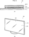
- Fig. 6(a) shows an example application of the capacitive sensor 1 to a touch panel 200.
- the touch panel 200 includes a display panel 210 and the capacitive sensor 1 on the display panel 210.
- the display panel 210 is, for example, a liquid crystal display panel.
- the display panel 210 composed of a liquid crystal display panel includes a drive substrate 211 and a counter substrate 212 that are disposed opposite each other and a liquid crystal layer 213 between the drive substrate 211 and the counter substrate 212.
- a touch sensor 220 is disposed on the front side of the counter substrate 212.
- Fig. 6(b) shows an example electronic device 300 including the touch panel 200.
- the electronic device 300 is, for example, a television.
- the electronic device 300 includes a housing 310 and a display unit 320.
- the touch panel 200 is disposed on the surface of the display unit 320.
- the electronic device 300 is not limited to a television, but may be another device such as a smartphone, cellular phone, or tablet terminal.
- the capacitive sensor 1 may also be applied to other applications, including electrical appliances such as refrigerators and washing machines and transportation equipment such as automobiles and ships.
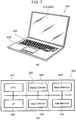
- Fig. 7(a) shows an example computer 400 (notebook computer) including the touch panel 200.
- the computer 400 includes, for example, a display 410, a keyboard 420, and an input pad 430.
- the computer 400 includes a central processing unit 401, a main memory 402, a sub memory 403, an input device 404, an output device 405, and an interface 406.
- the keyboard 420 and the input pad 430 are examples of the input device 404.
- the display 410 is an example of the output device 405.
- the display 410 includes the touch panel 200.
- the touch panel 200 is an example of a combination of the input device 404 and the output device 405.
- the capacitive sensor 1 can accurately determine the contact position and send input instructions to the device.
- this embodiment can provide a method for manufacturing a capacitive sensor by which capacitive sensors including bridge wiring lines at intersections of a plurality of electrode layers can be manufactured with high productivity, and can also provide a capacitive sensor and a photosensitive conductive sheet.
- the optical clear adhesive layer 30 is disposed between the structure including the first electrode strings 8 and the second electrode strings 12 disposed on the substrate 2 and the protective layer 3; however, the present invention is not limited to this configuration.
- the protective layer 3 may be disposed so as to cover the structure including the first electrode strings 8 and the second electrode strings 12 disposed on the substrate 2. This configuration can be obtained, for example, by applying a composition for forming the protective layer 3 to the above structure and curing the coating to form the protective layer 3.
- Fig. 8 is a schematic plan view of an example Kelvin pattern.
- a first sample 5S containing silver nanowires and a second sample 10S formed of zinc oxide were arranged so as to intersect each other.
- the first sample 5S corresponds to the second transparent electrodes 5.
- the second sample 10S corresponds to the first layer 101 (101a and 101b) of the bridge wiring parts 10.
- one of the length L11 of a contact portion P1 in the Y1-Y2 direction and the length L12 of the contact portion P1 in the X1-X2 direction was fixed at 100 ⁇ m, and the other of the length L11 and the length L12 was varied so that the contact portion P1 had varying contact areas. In this way, a plurality of kelvin patterns having contact portions P1 with different contact areas were provided.
- a plurality of kelvin patterns having contact portions P1 with different contact areas were provided as in Example 1 except that the second sample 10S was replaced with two types of comparative samples formed of indium tin oxide (ITO) that were manufactured by different methods.
- ITO indium tin oxide
- kelvin patterns were subjected to an environment test in which they were allowed to stand in an environment with a temperature of 85°C and a relative humidity of 85% for 240 hours (8585 reliability test).
- the electrical resistances Rc (unit: ⁇ ) of the contact portions P1 of the kelvin patterns after the test were measured.
- Fig. 9 is a graph showing the relationship between the contact area and the electrical resistance Rc of the contact portion P1 between the first sample 5S and the second sample 10S or the comparative samples.
- the electrical resistances Rc of the kelvin patterns of Example 1 were lower than those of the kelvin patterns of Comparative Examples 1 and 2 at any contact area.
Landscapes
- Engineering & Computer Science (AREA)
- General Engineering & Computer Science (AREA)
- Theoretical Computer Science (AREA)
- Human Computer Interaction (AREA)
- Physics & Mathematics (AREA)
- General Physics & Mathematics (AREA)
- Position Input By Displaying (AREA)
Abstract
Description
- The present invention relates to capacitive sensors, and particularly to a capacitive sensor having transparent electrodes containing conductive nanowires and a device including such a capacitive sensor.
-
PTL 1 discloses a finger-touch sensing panel having X and Y electrodes formed of indium tin oxide (ITO) layers on a transparent glass substrate. The finger-touch sensing panel described inPTL 1 has areas where the X and Y electrodes cross each other. The Y electrodes are electrically connected together by conductor films via openings. Thus, the X and Y electrodes cross each other on the substrate, and bridge wiring parts are provided to electrically connect the Y electrodes together, which allows for a reduction in the thickness of the sensing panel. - As the market trend, there is a need for curved capacitive sensors and flexible capacitive sensors. Accordingly, for example, materials containing conductive nanowires such as gold nanowires, silver nanowires, and copper nanowires are occasionally used as materials for transparent electrodes in capacitive sensors. Citation List
- PTL 1: Japanese Unexamined Patent Application Publication No.
58-166437 - However, the use of a material containing conductive nanowires as a material for transparent electrodes has a problem in that the contact area between the transparent electrodes and bridge wiring parts provided at the intersections of the electrodes is relatively narrow. Specifically, in the case of conductive nanowires, conductive wires exposed in the surfaces of the transparent electrodes are responsible for ensuring sufficient conductivity and transparency. Therefore, if the bridge wiring parts are formed of a material containing conductive nanowires, the contacts between the transparent electrodes and the bridge wiring parts are wire-to-wire contacts. Alternatively, if the bridge wiring parts are formed of, for example, an oxide-based material such as ITO, the contacts between the transparent electrodes and the bridge wiring parts are wire-to-surface contacts. Thus, the use of a material containing conductive nanowires as a material for the transparent electrodes results in a relatively narrow contact area between the transparent electrodes and the bridge wiring parts.
- Consequently, the conduction stability may decrease. In addition, if a large current flows through the contact portions between the transparent electrodes and the bridge wiring parts in the event of electrostatic discharge (ESD), the contact portions may heat up locally and may thus melt and break. That is, although the use of a material containing conductive nanowires as a material for the transparent electrodes improves the deformation performance of the capacitive sensor, its conduction stability and ESD tolerance may decrease. In addition, the use of a crystalline oxide-based material or metal-based material as a material for the bridge wiring parts may increase the resistance during bending and may also lead to a break in the bridge wiring parts.
- One possible solution to such problems is to increase the contact area between the transparent electrodes and the bridge wiring parts by increasing the size of the bridge wiring parts. Increasing the size of the bridge wiring parts, however, has a problem in that the bridge wiring parts become more visible.
- The present invention has been made to solve the foregoing problems with the conventional art. An object of the present invention is to provide a capacitive sensor with superior conduction stability and sufficient invisibility of bridge wiring parts and a device including such a capacitive sensor.
- One aspect of the present invention provides a capacitive sensor including a light-transmissive substrate; a plurality of first transparent electrodes arranged side by side in a sensing region of one main surface of the substrate in a first direction, the first transparent electrodes being light-transmissive; a plurality of second transparent electrodes arranged side by side in the sensing region in a second direction intersecting the first direction, the second transparent electrodes being light-transmissive and containing conductive nanowires; coupling parts provided integrally with the first transparent electrodes and electrically connecting two adjacent first transparent electrodes to each other; and bridge wiring parts provided independently of the second transparent electrodes so as to intersect the coupling parts and electrically connecting two adjacent second transparent electrodes to each other. Each of the bridge wiring parts is composed of two contact portions, each in contact with one of the two adjacent second transparent electrodes, and a bridge portion provided continuously with the contact portions and separated from the two adjacent second transparent electrodes. Each of the contact portions has a multilayer structure, and a layer including a portion in contact with the second transparent electrode is formed of a zinc-oxide-based material. A surface of the bridge portion located farther from the substrate is formed of an amorphous-oxide-based material.
- A layer formed of a zinc-oxide-based material tends to have a lower contact resistance with the second transparent electrodes containing the conductive nanowires than a layer formed of an amorphous-oxide-based material. On the other hand, a layer formed of a zinc-oxide-based material is more visible than a layer formed of an amorphous-oxide-based material. Accordingly, as described above, the layers of the bridge wiring parts that are in contact with the second transparent electrodes are formed of a zinc-oxide-based material to reduce the contact resistance between the bridge wiring parts and the second transparent electrodes, whereas the surfaces of the bridge wiring parts on the viewer side are formed of an amorphous-oxide-based material to enhance the invisibility of the bridge wiring parts. Thus, a capacitive sensor with superior conduction stability and sufficient invisibility of bridge wiring parts can be provided.
- A layer of each of the contact portions that is farthest from the second transparent electrodes is preferably formed of an amorphous-oxide-based material.
- The bridge portion may be formed of the amorphous-oxide-based material.
- The bridge portion may have a multilayer structure, and a layer provided continuously with the layers closest to the second transparent electrodes and formed of a zinc-oxide-based material may be located closer to the substrate than is a layer formed of the amorphous-oxide-based material.
- The zinc-oxide-based material may include at least one of zinc oxide and indium zinc oxide. The conductive nanowires may be at least one selected from the group consisting of gold nanowires, silver nanowires, and copper nanowires. The amorphous-oxide-based material may be at least one selected from the group consisting of amorphous ITO, amorphous GZO, amorphous AZO, and amorphous FTO.
- Another aspect of the present invention provides a device including the above capacitive sensor.
- According to the present invention, a capacitive sensor with superior conduction stability and sufficient invisibility of bridge wiring parts and a device including such a capacitive sensor can be provided.
-
-
Fig. 1 is a plan view of a capacitive sensor according to an embodiment. -
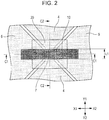
Fig. 2 is an enlarged plan view of an area A1 shown inFig. 1 . -
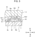
Fig. 3 is a sectional view taken along cross-section C1-C1 shown inFig. 2 . -
Fig. 4 is a sectional view taken along cross-section C2-C2 shown inFig. 2 . -
Fig. 5 is a partial sectional view, corresponding toFig. 3 , of a capacitive sensor according to a modification of the embodiment. -
Figs. 6(a) and 6(b) are schematic views of an example application. -
Figs. 7(a) and 7(b) are schematic views of an example application. -
Fig. 8 is a schematic plan view of an example Kelvin pattern. -
Fig. 9 is a graph showing the relationship between the contact area and the electrical resistance Rc of a contact portion P1. - An embodiment of the present invention will hereinafter be described with reference to the drawings. In the drawings, similar components are denoted by the same reference numerals, and a detailed description thereof is omitted where appropriate.
-
Fig. 1 is a plan view of a capacitive sensor according to this embodiment. -
Fig. 2 is an enlarged plan view of an area A1 shown inFig. 1 . -
Fig. 3 is a sectional view taken along cross-section C1-C1 shown inFig. 2 . -
Fig. 4 is a sectional view taken along cross-section C2-C2 shown inFig. 2 . - Although transparent electrodes are transparent and therefore invisible by nature, the contours of the transparent electrodes are shown in
Figs. 1 and2 for ease of understanding. - As used herein, "transparent" and "light-transmissive" refer to a visible light transmittance of 50% or more (preferably 80% or more). In addition, a haze of 6% or less is suitable. As used herein, "block light" and "light-blocking" refer to a visible light transmittance of less than 50% (preferably less than 20%).
- As shown in
Figs. 1 to 4 , acapacitive sensor 1 according to this embodiment includes asubstrate 2, firsttransparent electrodes 4, secondtransparent electrodes 5,coupling parts 7,bridge wiring parts 10, and aprotective layer 3. An opticalclear adhesive layer 30 is disposed between thesubstrate 2 and theprotective layer 3. Insulatinglayers 20 are disposed between thesubstrate 2 and thebridge wiring parts 10. As shown inFig. 3 , the opticalclear adhesive layer 30 is disposed between thebridge wiring parts 10 and theprotective layer 3 in the areas where thebridge wiring parts 10 are disposed. - The
substrate 2 is light-transmissive and is formed of, for example, a film-shaped transparent substrate such as a polyethylene terephthalate (PET) film or a glass substrate. The firsttransparent electrodes 4 and the secondtransparent electrodes 5 are disposed on onemain surface 2a of thesubstrate 2. The details will be described later. As shown inFig. 3 , theprotective layer 3 is disposed on the side of thebridge wiring parts 10 facing away from the substrate and is light-transmissive. Examples of materials for theprotective layer 3 include light-transmissive plastic substrates such as polycarbonate substrates. Theprotective layer 3 is bonded to thesubstrate 2 with the optical clear adhesive (OCA)layer 30 disposed between thesubstrate 2 and theprotective layer 3. The optical clear adhesive (OCA)layer 30 is formed of, for example, an adhesive layer containing an acrylic adhesive or a double-sided acrylic tape. - As shown in
Fig. 1 , thecapacitive sensor 1 is composed of asensing region 11 and anon-sensing region 25 as viewed in the direction normal to the surface on theprotective layer 3 side (Z1-Z2 direction). Thesensing region 11 is a region that can be manipulated by a manipulating object such as a finger. Thenon-sensing region 25 is a frame-shaped region located outside thesensing region 11. In thenon-sensing region 25, light is blocked by a decorative layer (not shown). Thus, light traveling from the surface on theprotective layer 3 side toward the surface on thesubstrate 2 side of the capacitive sensor 1 (e.g., external light) and light traveling from the surface on thesubstrate 2 side toward the surface on theprotective layer 3 side of the capacitive sensor 1 (e.g., light coming from a backlight of a display device used in combination with the capacitive sensor 1) are unlikely to pass through thenon-sensing region 25. - As shown in
Fig. 1 ,first electrode strings 8 and second electrode strings 12 are disposed on themain surface 2a of thesubstrate 2. Thefirst electrode strings 8 are arranged in thesensing region 11 and include a plurality of firsttransparent electrodes 4. As shown inFigs. 3 and4 , of the main surfaces of thesubstrate 2 to which the direction along the Z1-Z2 direction is normal, the plurality of firsttransparent electrodes 4 are disposed on themain surface 2a located on the Z1 side (which may be hereinafter abbreviated as "front surface"). The individual firsttransparent electrodes 4 are coupled together via theelongated coupling parts 7 in the Y1-Y2 direction (first direction). Thefirst electrode strings 8, which include the plurality of firsttransparent electrodes 4 coupled together in the Y1-Y2 direction, are arranged at a distance from each other in the X1-X2 direction. Thecoupling parts 7 are formed integrally with the firsttransparent electrodes 4. Thecoupling parts 7 electrically connect two adjacent firsttransparent electrodes 4 to each other. - The first
transparent electrodes 4 and thecoupling parts 7 are light-transmissive and are formed of a material containing conductive nanowires. The conductive nanowires are at least one selected from the group consisting of gold nanowires, silver nanowires, and copper nanowires. The use of a material containing conductive nanowires allows the firsttransparent electrodes 4 to have high light transmissivity and low electrical resistance. In addition, the use of a material containing conductive nanowires improves the deformation performance of thecapacitive sensor 1. - The material containing the conductive nanowires includes conductive nanowires and a transparent resin layer. The conductive nanowires are dispersed in the resin layer. The resin layer ensures the dispersibility of the conductive nanowires. Examples of materials for the transparent resin layer include polyester resins, acrylic resins, and polyurethane resins. A plurality of conductive nanowires are at least partially in contact with each other, thus maintaining the in-plane conductivity of the material containing the conductive nanowires.
- The second electrode strings 12 are arranged in the
sensing region 11 and include a plurality of secondtransparent electrodes 5. As shown inFigs. 3 and4 , the plurality of secondtransparent electrodes 5 are disposed on thefront surface 2a of thesubstrate 2. Thus, the secondtransparent electrodes 5 are disposed on the same surface as the first transparent electrodes 4 (thefront surface 2a of the substrate 2). The individual secondtransparent electrodes 5 are coupled together via the elongatedbridge wiring parts 10 in the X1-X2 direction (second direction). The second electrode strings 12, which include the plurality of secondtransparent electrodes 5 coupled together in the X1-X2 direction, are arranged at a distance from each other in the Y1-Y2 direction. Thebridge wiring parts 10 are formed independently of the secondtransparent electrodes 5. The X1-X2 direction intersects the Y1-Y2 direction. For example, the X1-X2 direction intersects the Y1-Y2 direction perpendicularly. - The second
transparent electrodes 5 are light-transmissive and are formed of a material containing conductive nanowires. The conductive nanowires are as described above for the material for the firsttransparent electrodes 4. - As shown in
Fig. 3 , each of thebridge wiring parts 10 is composed of two contact portions 10A1 and 10A2, each in contact with one of the two adjacent secondtransparent electrodes bridge portion 10B provided continuously with the contact portions 10A1 and 10A2 and separated from the two adjacent secondtransparent electrodes - Each of the contact portions 10A1 and 10A2 has a multilayer structure. Specifically, each of the contact portions 10A1 and 10A2 includes at least a layer in contact with the second
transparent electrode 5 and a layer different from that layer and located farther from the secondtransparent electrode 5. In the case of the structure shown inFig. 3 , each of thebridge wiring parts 10 is composed, in its entirety, of a layer (first layer) 101 including portions in contact with the secondtransparent electrodes 5 and asecond layer 102 located farther than thefirst layer 101. - The
first layer 101 is formed of a zinc-oxide-based material. Although the reason is not fully understood, a layer formed of a zinc-oxide-based material tends to have a lower contact resistance with the secondtransparent electrodes 5 containing the conductive nanowires. In particular, the contact resistance tends not to increase after a test is carried out in a high-temperature, hard (e.g., 85°C and a relative humidity of 85%) environment (8585 test) for a long period of time (e.g., 100 hours). Specifically, a layer formed of a zinc-oxide-based material has a lower contact resistance with the secondtransparent electrodes 5 containing the conductive nanowires after an 8585 test than a layer formed of indium tin oxide (ITO), which is a typical transparent conductive material. Thus, the use of a zinc-oxide-based material as a material for the layer (first layer) 101 including portions in contact with the secondtransparent electrodes 5 allows for a reduction in the resistance between the two adjacent secondtransparent electrodes - The surface (farther surface) 10a of the
bridge wiring parts 10 located farther from thesubstrate 2 is formed of an amorphous-oxide-based material. In the case of the structure shown inFig. 3 , thefarther surface 10a is the surface of thesecond layer 102; therefore, thesecond layer 102 is formed of an amorphous-oxide-based material. Amorphous-oxide-based materials are less visible than zinc-oxide-based materials. Therefore, if thefarther surface 10a is formed of an amorphous-oxide-based material, the visibility of thebridge wiring part 10 can be reduced. Specific examples of amorphous-oxide-based materials include amorphous indium tin oxide (ITO), amorphous gallium-doped zinc oxide (GZO), amorphous aluminum-doped zinc oxide (AZO), and amorphous fluorine-doped zinc oxide (FTO). -
Fig. 5 is a partial sectional view, corresponding toFig. 3 , of a capacitive sensor according to a modification of this embodiment. As shown inFig. 5 , in each of thebridge wiring parts 10 of the capacitive sensor according to this modification, the contact portion 10A1 has a multilayer structure composed of a first layer 101a and thesecond layer 102, and the contact portion 10A2 has a multilayer structure composed of afirst layer 101b and thesecond layer 102. In contrast, thebridge portion 10B has a single-layer structure composed of thesecond layer 102. It is preferred that thefirst layers 101a and 101b, which are formed of a zinc-oxide-based material, be present in the contact portions 10A1 and 10A2 since the contact resistance with the secondtransparent electrodes 5 can be reduced. However, thefirst layers 101a and 101b are more visible than thesecond layer 102, which is formed of an amorphous-oxide-based material. Thus, a layer formed of a zinc-oxide-based material need not necessarily be located in thebridge portion 10B, as long as thesecond layer 102, which is formed of an amorphous-oxide-based material and is therefore relatively invisible, is located in thebridge portion 10B. - The
bridge wiring parts 10 may include layers other than the first layer 101 (101a and 101b), which is formed of a zinc-oxide-based material, and thesecond layer 102, which is formed of an amorphous-oxide-based material. Examples of such layers include layers formed of metals that have lower resistance and higher transparency than the first layer 101 (101a and 101b) and thesecond layer 102. - As shown in
Figs. 2 to 4 , the insulatinglayers 20 are disposed over the surfaces of thecoupling parts 7 coupling the individual firsttransparent electrodes 4. As shown inFig. 3 , the insulatinglayers 20 fill the spaces between thecoupling parts 7 and the secondtransparent electrodes 5 and also extend to some extent onto the surfaces of the secondtransparent electrodes 5. The insulating layers 20 are formed of, for example, a novolac resin (resist). - As shown in
Figs. 3 and4 , thebridge wiring parts 10 extend from thesurfaces 20a of the insulatinglayers 20 to the surfaces of the secondtransparent electrodes 5 located on both sides of the insulatinglayers 20 in the X1-X2 direction. Thebridge wiring parts 10 electrically connect two adjacent secondtransparent electrodes 5 to each other. - As shown in
Figs. 3 and4 , the insulatinglayers 20 are disposed over the surfaces of thecoupling parts 7 connecting the individual firsttransparent electrodes 4, and thebridge wiring parts 10 connecting the individual secondtransparent electrodes 5 are disposed on the surfaces of the insulating layers 20. Thus, the insulatinglayers 20 are disposed between thecoupling parts 7 and thebridge wiring parts 10 and electrically insulate the firsttransparent electrodes 4 from the secondtransparent electrodes 5. In this embodiment, the firsttransparent electrodes 4 and the secondtransparent electrodes 5 are disposed on the same surface (thefront surface 2a of the substrate 2), which allows for a reduction in the thickness of thecapacitive sensor 1. - The
coupling parts 7 shown inFigs. 2 to 4 are formed integrally with the firsttransparent electrodes 4 and extend in the Y1-Y2 direction. Thebridge wiring parts 10 shown inFigs. 2 to 4 are formed independently of the secondtransparent electrodes 5 on thesurfaces 20a of the insulatinglayers 20 covering thecoupling parts 7 and extend in the X1-X2 direction. Thecoupling parts 7 and thebridge wiring parts 10, however, are not limited to this arrangement. For example, thecoupling parts 7 may be formed integrally with the firsttransparent electrodes 4 and may extend in the X1-X2 direction. In this case, thecoupling parts 7 electrically connect two adjacent secondtransparent electrodes 5 to each other. Thebridge wiring parts 10 may be formed independently of the firsttransparent electrodes 4 on thesurfaces 20a of the insulatinglayers 20 covering thecoupling parts 7 and may extend in the Y1-Y2 direction. In this case, thebridge wiring parts 10 electrically connect two adjacent firsttransparent electrodes 4 to each other. The description of thecapacitive sensor 1 according to this embodiment provides an example in which thebridge wiring parts 10 are formed independently of the secondtransparent electrodes 5 on thesurfaces 20a of the insulatinglayers 20 covering thecoupling parts 7 and extend in the X1-X2 direction. - As shown in
Fig. 1 , a plurality ofwiring parts 6 routed from thefirst electrode strings 8 and the second electrode strings 12 are formed in thenon-sensing region 25. Thefirst electrode strings 8 and the second electrode strings 12 are electrically connected to thewiring parts 6 via connection wiring lines 16. Thewiring parts 6 are connected toexternal connection parts 27 electrically connected to a flexible printed board (not shown). That is, thewiring parts 6 electrically connect thefirst electrode strings 8 and the second electrode strings 12 to theexternal connection parts 27. Theexternal connection parts 27 are electrically connected to the flexible printed board (not shown), for example, via conductive paste. - The
wiring parts 6 are formed of a material including a metal such as Cu, a Cu alloy, a CuNi alloy, Ni, Ag, or Au. Theconnection wiring lines 16 are formed of a transparent conductive material such as ITO and extend from thesensing region 11 into thenon-sensing region 25. Thewiring parts 6 overlie theconnection wiring lines 16 in thenon-sensing region 25 and are electrically connected to the connection wiring lines 16. - The
wiring parts 6 are disposed within thenon-sensing region 25 of thefront surface 2a of thesubstrate 2. As with thewiring parts 6, theexternal connection parts 27 are disposed within thenon-sensing region 25 of thefront surface 2a of thesubstrate 2. - In
Fig. 1 , thewiring parts 6 and theexternal connection parts 27 are shown as visible for ease of understanding; in practice, a light-blocking decorative layer (not shown) is disposed within thenon-sensing region 25. Thus, as thecapacitive sensor 1 is viewed from theprotective layer 3 side, thewiring parts 6 and theexternal connection parts 27 are hidden and made invisible by the decorative layer. The decorative layer may be formed of any light-blocking material. The decorative layer may have insulating properties. - As shown in
Fig. 3 , for example, when a finger, which is an example of a manipulating object, touches thesurface 3a of theprotective layer 3 of thecapacitive sensor 1 according to this embodiment, capacitors are formed between the finger and the firsttransparent electrode 4 close to the finger and between the finger and the secondtransparent electrode 5 close to the finger. Based on the resulting change in capacitance, thecapacitive sensor 1 can calculate the position touched by the finger. Thecapacitive sensor 1 determines the X coordinate of the finger position based on the change in capacitance between the finger and thefirst electrode strings 8 and determines the Y coordinate of the finger position based on the change in capacitance between the finger and the second electrode strings 12 (self-capacitance sensing type). - Alternatively, the
capacitive sensor 1 may be of mutual capacitance sensing type. Specifically, thecapacitive sensor 1 may apply a drive voltage to one electrode string of one of thefirst electrode strings 8 and the second electrode strings 12 and sense the change in capacitance between the electrodes of the other of thefirst electrode strings 8 and the second electrode strings 12 and the finger. In this way, thecapacitive sensor 1 determines the X coordinate of the finger position using one type of electrode and determines the Y coordinate of the finger position using the other type of electrode. - Next, example applications of the
capacitive sensor 1 according to this embodiment will be described.Figs. 6(a) to 7(b) are schematic views of example applications. -
Fig. 6(a) shows an example application of thecapacitive sensor 1 to atouch panel 200. Thetouch panel 200 includes adisplay panel 210 and thecapacitive sensor 1 on thedisplay panel 210. Thedisplay panel 210 is, for example, a liquid crystal display panel. Thedisplay panel 210 composed of a liquid crystal display panel includes a drive substrate 211 and acounter substrate 212 that are disposed opposite each other and aliquid crystal layer 213 between the drive substrate 211 and thecounter substrate 212. Atouch sensor 220 is disposed on the front side of thecounter substrate 212. -
Fig. 6(b) shows an exampleelectronic device 300 including thetouch panel 200. Theelectronic device 300 is, for example, a television. Theelectronic device 300 includes ahousing 310 and adisplay unit 320. Thetouch panel 200 is disposed on the surface of thedisplay unit 320. Theelectronic device 300 is not limited to a television, but may be another device such as a smartphone, cellular phone, or tablet terminal. Thecapacitive sensor 1 may also be applied to other applications, including electrical appliances such as refrigerators and washing machines and transportation equipment such as automobiles and ships. -
Fig. 7(a) shows an example computer 400 (notebook computer) including thetouch panel 200. Thecomputer 400 includes, for example, adisplay 410, akeyboard 420, and aninput pad 430. As shown inFig. 7(b) , thecomputer 400 includes acentral processing unit 401, amain memory 402, asub memory 403, aninput device 404, anoutput device 405, and aninterface 406. Thekeyboard 420 and theinput pad 430 are examples of theinput device 404. Thedisplay 410 is an example of theoutput device 405. Thedisplay 410 includes thetouch panel 200. Thetouch panel 200 is an example of a combination of theinput device 404 and theoutput device 405. - If the
capacitive sensor 1 according to this embodiment is applied to such a device, thecapacitive sensor 1 can accurately determine the contact position and send input instructions to the device. - As described above, this embodiment can provide a method for manufacturing a capacitive sensor by which capacitive sensors including bridge wiring lines at intersections of a plurality of electrode layers can be manufactured with high productivity, and can also provide a capacitive sensor and a photosensitive conductive sheet.
- Although embodiments and example applications thereof have been described above, these examples are not intended to limit the present invention. For example, suitable additions, deletions, and design changes to the elements of the foregoing embodiments and example applications thereof and suitable combinations of the features of the embodiments that are made by those skilled in the art are also included in the scope of the present invention as long as they possess the spirit of the present invention. For example, in the foregoing description, the optical
clear adhesive layer 30 is disposed between the structure including thefirst electrode strings 8 and the second electrode strings 12 disposed on thesubstrate 2 and theprotective layer 3; however, the present invention is not limited to this configuration. Theprotective layer 3 may be disposed so as to cover the structure including thefirst electrode strings 8 and the second electrode strings 12 disposed on thesubstrate 2. This configuration can be obtained, for example, by applying a composition for forming theprotective layer 3 to the above structure and curing the coating to form theprotective layer 3. - The present invention will now be more specifically described with reference to the following Example and other examples, although they are not intended to limit the scope of the present invention.
-
Fig. 8 is a schematic plan view of an example Kelvin pattern. Using the kelvin pattern shown inFig. 8 , afirst sample 5S containing silver nanowires and asecond sample 10S formed of zinc oxide were arranged so as to intersect each other. Thefirst sample 5S corresponds to the secondtransparent electrodes 5. Thesecond sample 10S corresponds to the first layer 101 (101a and 101b) of thebridge wiring parts 10. In this test, one of the length L11 of a contact portion P1 in the Y1-Y2 direction and the length L12 of the contact portion P1 in the X1-X2 direction was fixed at 100 µm, and the other of the length L11 and the length L12 was varied so that the contact portion P1 had varying contact areas. In this way, a plurality of kelvin patterns having contact portions P1 with different contact areas were provided. - A plurality of kelvin patterns having contact portions P1 with different contact areas were provided as in Example 1 except that the
second sample 10S was replaced with two types of comparative samples formed of indium tin oxide (ITO) that were manufactured by different methods. (Measurement Example) Electrical Resistance Measurement after 8585 Reliability Test - The kelvin patterns were subjected to an environment test in which they were allowed to stand in an environment with a temperature of 85°C and a relative humidity of 85% for 240 hours (8585 reliability test). The electrical resistances Rc (unit: Ω) of the contact portions P1 of the kelvin patterns after the test were measured.
Fig. 9 is a graph showing the relationship between the contact area and the electrical resistance Rc of the contact portion P1 between thefirst sample 5S and thesecond sample 10S or the comparative samples. - As shown in
Fig. 9 , the electrical resistances Rc of the kelvin patterns of Example 1 were lower than those of the kelvin patterns of Comparative Examples 1 and 2 at any contact area. -
- 1
- capacitive sensor
- 2
- substrate
- 2a
- main surface (front surface)
- 3
- protective layer
- 3a
- surface
- 4
- first transparent electrode
- 5
- second transparent electrode
- 5S
- first sample
- 6
- wiring part
- 7
- coupling part
- 8
- first electrode string
- 10
- bridge wiring part
- 10A1, 10A2
- contact portion
- 10B
- bridge portion
- 101, 101a, 101b
- first layer
- 10a
- farther surface
- 102
- second layer
- 10S
- second sample
- 11
- sensing region
- 12
- second electrode string
- 16
- connection wiring line
- 20
- insulating layer
- 20a
- surface
- 25
- non-sensing region
- 27
- external connection part
- 30
- optical clear adhesive layer
- A1
- area
- C1
- cross-section
- C2
- cross-section
- L11
- size
- L12
- size
- P1
- contact portion
- 200
- touch panel
- 210
- display panel
- 211
- drive substrate
- 212
- counter substrate
- 213
- liquid crystal layer
- 220
- touch sensor
- 300
- electronic device
- 310
- housing
- 320
- display unit
- 400
- computer
- 410
- display
- 420
- keyboard
- 430
- input pad
- 401
- central processing unit
- 402
- main memory
- 403
- sub memory
- 404
- input device
- 405
- output device
- 406
- interface
Claims (8)
- A capacitive sensor comprising:a light-transmissive substrate;a plurality of first transparent electrodes arranged side by side in a sensing region of one main surface of the substrate in a first direction, the first transparent electrodes being light-transmissive;a plurality of second transparent electrodes arranged side by side in the sensing region in a second direction intersecting the first direction, the second transparent electrodes being light-transmissive and comprising conductive nanowires;coupling parts provided integrally with the first transparent electrodes and electrically connecting two adjacent first transparent electrodes to each other; andbridge wiring parts provided independently of the second transparent electrodes so as to intersect the coupling parts and electrically connecting two adjacent second transparent electrodes to each other,wherein each of the bridge wiring parts comprises two contact portions, each in contact with one of the two adjacent second transparent electrodes, and a bridge portion provided continuously with the contact portions and separated from the two adjacent second transparent electrodes,each of the contact portions has a multilayer structure, and a layer including a portion in contact with the second transparent electrode comprises a zinc-oxide-based material, anda surface of the bridge portion located farther from the substrate comprises an amorphous-oxide-based material.
- The capacitive sensor according to Claim 1, wherein a layer of each of the contact portions that is farthest from the second transparent electrodes comprises an amorphous-oxide-based material.
- The capacitive sensor according to Claim 1 or 2, wherein the bridge portion comprises the amorphous-oxide-based material.
- The capacitive sensor according to any one of Claims 1 to 3, wherein the bridge portion has a multilayer structure, and a layer provided continuously with the layers closest to the second transparent electrodes and comprising a zinc-oxide-based material is located closer to the substrate than is a layer comprising the amorphous-oxide-based material.
- The capacitive sensor according to Claim 1, wherein the zinc-oxide-based material comprises at least one of zinc oxide and indium zinc oxide.
- The capacitive sensor according to Claim 1, wherein the conductive nanowires are at least one selected from the group consisting of gold nanowires, silver nanowires, and copper nanowires.
- The capacitive sensor according to Claim 1 or 2, wherein the amorphous-oxide-based material is at least one selected from the group consisting of amorphous ITO, amorphous GZO, amorphous AZO, and amorphous FTO.
- A device comprising the capacitive sensor according to any one of Claims 1 to 7.
Applications Claiming Priority (2)
| Application Number | Priority Date | Filing Date | Title |
|---|---|---|---|
| JP2016240674 | 2016-12-12 | ||
| PCT/JP2017/039153 WO2018110123A1 (en) | 2016-12-12 | 2017-10-30 | Capacitance-type sensor and device |
Publications (2)
| Publication Number | Publication Date |
|---|---|
| EP3553641A1 true EP3553641A1 (en) | 2019-10-16 |
| EP3553641A4 EP3553641A4 (en) | 2020-06-24 |
Family
ID=62558569
Family Applications (1)
| Application Number | Title | Priority Date | Filing Date |
|---|---|---|---|
| EP17879772.6A Withdrawn EP3553641A4 (en) | 2016-12-12 | 2017-10-30 | Capacitance-type sensor and device |
Country Status (6)
| Country | Link |
|---|---|
| US (1) | US10684735B2 (en) |
| EP (1) | EP3553641A4 (en) |
| JP (1) | JP6735850B2 (en) |
| KR (1) | KR20190065390A (en) |
| CN (1) | CN110023892A (en) |
| WO (1) | WO2018110123A1 (en) |
Families Citing this family (5)
| Publication number | Priority date | Publication date | Assignee | Title |
|---|---|---|---|---|
| DE112020004388T5 (en) | 2019-09-18 | 2022-06-02 | Alps Alpine Co., Ltd. | Electrostatic capacitance sensor and input device |
| WO2021075304A1 (en) * | 2019-10-18 | 2021-04-22 | 富士フイルム株式会社 | Transparent multilayer body and image display device |
| TW202201772A (en) * | 2020-06-22 | 2022-01-01 | 瑞典商斯莫勒科技公司 | Image sensor with nanostructure-based capacitors |
| TWI770800B (en) * | 2021-02-02 | 2022-07-11 | 大陸商宸美(廈門)光電有限公司 | Electronic device |
| US11513646B2 (en) | 2021-03-02 | 2022-11-29 | Tpk Advanced Solutions Inc. | Electronic device |
Family Cites Families (9)
| Publication number | Priority date | Publication date | Assignee | Title |
|---|---|---|---|---|
| JPS58166437A (en) | 1982-03-26 | 1983-10-01 | Fujitsu Ltd | Manufacture of finger touch type coordinate detection panel |
| CN102243553B (en) * | 2010-05-16 | 2015-06-10 | 宸鸿科技(厦门)有限公司 | Capacitive touch panel and method for reducing visuality of metal conductor of capacitive touch panel |
| JP5865819B2 (en) * | 2012-02-10 | 2016-02-17 | アルプス電気株式会社 | Input device |
| JP5803825B2 (en) * | 2012-06-28 | 2015-11-04 | 日立化成株式会社 | Capacitive coupling type touch panel and manufacturing method thereof |
| CN104699285B (en) * | 2013-12-09 | 2017-11-21 | 宸鸿科技(厦门)有限公司 | Touch-control sensing structure and forming method thereof |
| JP2015118537A (en) * | 2013-12-18 | 2015-06-25 | 大日本印刷株式会社 | Display device with touch panel sensor and touch position detection function |
| KR102263975B1 (en) * | 2014-12-16 | 2021-06-11 | 삼성디스플레이 주식회사 | Touch panel and method of manufacturing the same |
| CN106919278A (en) * | 2015-12-28 | 2017-07-04 | 宸鸿科技(厦门)有限公司 | Contact panel |
| KR102285533B1 (en) * | 2016-10-06 | 2021-08-03 | 알프스 알파인 가부시키가이샤 | capacitive sensor |
-
2017
- 2017-10-30 WO PCT/JP2017/039153 patent/WO2018110123A1/en not_active Ceased
- 2017-10-30 JP JP2018556238A patent/JP6735850B2/en not_active Expired - Fee Related
- 2017-10-30 EP EP17879772.6A patent/EP3553641A4/en not_active Withdrawn
- 2017-10-30 CN CN201780072509.9A patent/CN110023892A/en not_active Withdrawn
- 2017-10-30 KR KR1020197013382A patent/KR20190065390A/en not_active Abandoned
-
2019
- 2019-05-16 US US16/414,288 patent/US10684735B2/en not_active Expired - Fee Related
Also Published As
| Publication number | Publication date |
|---|---|
| WO2018110123A1 (en) | 2018-06-21 |
| EP3553641A4 (en) | 2020-06-24 |
| US20190272054A1 (en) | 2019-09-05 |
| KR20190065390A (en) | 2019-06-11 |
| CN110023892A (en) | 2019-07-16 |
| US10684735B2 (en) | 2020-06-16 |
| JP6735850B2 (en) | 2020-08-05 |
| JPWO2018110123A1 (en) | 2019-07-11 |
Similar Documents
| Publication | Publication Date | Title |
|---|---|---|
| US10684735B2 (en) | Capacitive sensor and device | |
| US10048820B2 (en) | Touch panel and manufacturing method thereof | |
| CN103186271B (en) | Contact panel and preparation method thereof | |
| US20180210575A1 (en) | Touch screen, method for manufacturing touch screen, and touch display device | |
| EP2333649A2 (en) | Capacitive touch device structure | |
| JP3153971U (en) | Touchpad | |
| KR102285533B1 (en) | capacitive sensor | |
| TWI628563B (en) | Touch-sensing electrode and touch screen panel including the same | |
| CN110858107A (en) | touch display device | |
| JP2013178738A (en) | Input device | |
| CN109074195B (en) | Electrostatic capacitance type sensor | |
| TWI486859B (en) | Capacitive touch panel structure | |
| US20140320758A1 (en) | Touch panel | |
| CN105468184A (en) | Transparent electrode layer laminate and touch screen panel comprising same | |
| TW201530410A (en) | Touch sensor | |
| CN202217247U (en) | Jumper structure arranged on flexible substrate, and flexible touch induction plate | |
| CN111596789A (en) | Touch panel, touch display panel and touch display device | |
| CN104714678A (en) | Touch panel, touch display device and manufacturing method of touch panel | |
| CN204203938U (en) | Touch panel structure | |
| TW201349072A (en) | Capacitive touch panel unit |
Legal Events
| Date | Code | Title | Description |
|---|---|---|---|
| STAA | Information on the status of an ep patent application or granted ep patent |
Free format text: STATUS: THE INTERNATIONAL PUBLICATION HAS BEEN MADE |
|
| PUAI | Public reference made under article 153(3) epc to a published international application that has entered the european phase |
Free format text: ORIGINAL CODE: 0009012 |
|
| STAA | Information on the status of an ep patent application or granted ep patent |
Free format text: STATUS: REQUEST FOR EXAMINATION WAS MADE |
|
| 17P | Request for examination filed |
Effective date: 20190611 |
|
| AK | Designated contracting states |
Kind code of ref document: A1 Designated state(s): AL AT BE BG CH CY CZ DE DK EE ES FI FR GB GR HR HU IE IS IT LI LT LU LV MC MK MT NL NO PL PT RO RS SE SI SK SM TR |
|
| AX | Request for extension of the european patent |
Extension state: BA ME |
|
| DAV | Request for validation of the european patent (deleted) | ||
| DAX | Request for extension of the european patent (deleted) | ||
| A4 | Supplementary search report drawn up and despatched |
Effective date: 20200528 |
|
| RIC1 | Information provided on ipc code assigned before grant |
Ipc: B32B 7/12 20060101ALI20200520BHEP Ipc: B32B 27/08 20060101ALI20200520BHEP Ipc: B32B 27/36 20060101ALI20200520BHEP Ipc: G06F 3/044 20060101AFI20200520BHEP |
|
| STAA | Information on the status of an ep patent application or granted ep patent |
Free format text: STATUS: THE APPLICATION HAS BEEN WITHDRAWN |
|
| 18W | Application withdrawn |
Effective date: 20201112 |