EP3553555A1 - 3d-sensorsystem - Google Patents
3d-sensorsystem Download PDFInfo
- Publication number
- EP3553555A1 EP3553555A1 EP18181799.0A EP18181799A EP3553555A1 EP 3553555 A1 EP3553555 A1 EP 3553555A1 EP 18181799 A EP18181799 A EP 18181799A EP 3553555 A1 EP3553555 A1 EP 3553555A1
- Authority
- EP
- European Patent Office
- Prior art keywords
- sensing system
- mems
- light source
- scanning mirror
- scan
- Prior art date
- Legal status (The legal status is an assumption and is not a legal conclusion. Google has not performed a legal analysis and makes no representation as to the accuracy of the status listed.)
- Withdrawn
Links
- 239000000725 suspension Substances 0.000 claims description 6
- 238000004377 microelectronic Methods 0.000 claims description 3
- 230000004913 activation Effects 0.000 claims description 2
- 230000000295 complement effect Effects 0.000 claims description 2
- 239000004065 semiconductor Substances 0.000 claims description 2
- 238000010586 diagram Methods 0.000 description 18
- 238000000034 method Methods 0.000 description 12
- 238000005516 engineering process Methods 0.000 description 5
- 238000002366 time-of-flight method Methods 0.000 description 3
- 239000007787 solid Substances 0.000 description 2
- XUIMIQQOPSSXEZ-UHFFFAOYSA-N Silicon Chemical compound [Si] XUIMIQQOPSSXEZ-UHFFFAOYSA-N 0.000 description 1
- 230000003190 augmentative effect Effects 0.000 description 1
- 230000001419 dependent effect Effects 0.000 description 1
- 238000011161 development Methods 0.000 description 1
- 230000018109 developmental process Effects 0.000 description 1
- 230000000694 effects Effects 0.000 description 1
- 230000001815 facial effect Effects 0.000 description 1
- 238000005305 interferometry Methods 0.000 description 1
- 238000004519 manufacturing process Methods 0.000 description 1
- 230000010355 oscillation Effects 0.000 description 1
- 229910052710 silicon Inorganic materials 0.000 description 1
- 239000010703 silicon Substances 0.000 description 1
- 235000012431 wafers Nutrition 0.000 description 1
Images





Classifications
-
- G—PHYSICS
- G02—OPTICS
- G02B—OPTICAL ELEMENTS, SYSTEMS OR APPARATUS
- G02B26/00—Optical devices or arrangements for the control of light using movable or deformable optical elements
- G02B26/08—Optical devices or arrangements for the control of light using movable or deformable optical elements for controlling the direction of light
- G02B26/0816—Optical devices or arrangements for the control of light using movable or deformable optical elements for controlling the direction of light by means of one or more reflecting elements
- G02B26/0833—Optical devices or arrangements for the control of light using movable or deformable optical elements for controlling the direction of light by means of one or more reflecting elements the reflecting element being a micromechanical device, e.g. a MEMS mirror, DMD
-
- G—PHYSICS
- G01—MEASURING; TESTING
- G01S—RADIO DIRECTION-FINDING; RADIO NAVIGATION; DETERMINING DISTANCE OR VELOCITY BY USE OF RADIO WAVES; LOCATING OR PRESENCE-DETECTING BY USE OF THE REFLECTION OR RERADIATION OF RADIO WAVES; ANALOGOUS ARRANGEMENTS USING OTHER WAVES
- G01S1/00—Beacons or beacon systems transmitting signals having a characteristic or characteristics capable of being detected by non-directional receivers and defining directions, positions, or position lines fixed relatively to the beacon transmitters; Receivers co-operating therewith
- G01S1/70—Beacons or beacon systems transmitting signals having a characteristic or characteristics capable of being detected by non-directional receivers and defining directions, positions, or position lines fixed relatively to the beacon transmitters; Receivers co-operating therewith using electromagnetic waves other than radio waves
- G01S1/703—Details
- G01S1/7032—Transmitters
-
- G—PHYSICS
- G01—MEASURING; TESTING
- G01S—RADIO DIRECTION-FINDING; RADIO NAVIGATION; DETERMINING DISTANCE OR VELOCITY BY USE OF RADIO WAVES; LOCATING OR PRESENCE-DETECTING BY USE OF THE REFLECTION OR RERADIATION OF RADIO WAVES; ANALOGOUS ARRANGEMENTS USING OTHER WAVES
- G01S17/00—Systems using the reflection or reradiation of electromagnetic waves other than radio waves, e.g. lidar systems
- G01S17/02—Systems using the reflection of electromagnetic waves other than radio waves
- G01S17/06—Systems determining position data of a target
- G01S17/42—Simultaneous measurement of distance and other co-ordinates
-
- G—PHYSICS
- G01—MEASURING; TESTING
- G01S—RADIO DIRECTION-FINDING; RADIO NAVIGATION; DETERMINING DISTANCE OR VELOCITY BY USE OF RADIO WAVES; LOCATING OR PRESENCE-DETECTING BY USE OF THE REFLECTION OR RERADIATION OF RADIO WAVES; ANALOGOUS ARRANGEMENTS USING OTHER WAVES
- G01S5/00—Position-fixing by co-ordinating two or more direction or position line determinations; Position-fixing by co-ordinating two or more distance determinations
- G01S5/16—Position-fixing by co-ordinating two or more direction or position line determinations; Position-fixing by co-ordinating two or more distance determinations using electromagnetic waves other than radio waves
-
- G—PHYSICS
- G01—MEASURING; TESTING
- G01S—RADIO DIRECTION-FINDING; RADIO NAVIGATION; DETERMINING DISTANCE OR VELOCITY BY USE OF RADIO WAVES; LOCATING OR PRESENCE-DETECTING BY USE OF THE REFLECTION OR RERADIATION OF RADIO WAVES; ANALOGOUS ARRANGEMENTS USING OTHER WAVES
- G01S7/00—Details of systems according to groups G01S13/00, G01S15/00, G01S17/00
- G01S7/48—Details of systems according to groups G01S13/00, G01S15/00, G01S17/00 of systems according to group G01S17/00
- G01S7/481—Constructional features, e.g. arrangements of optical elements
- G01S7/4817—Constructional features, e.g. arrangements of optical elements relating to scanning
-
- H—ELECTRICITY
- H04—ELECTRIC COMMUNICATION TECHNIQUE
- H04N—PICTORIAL COMMUNICATION, e.g. TELEVISION
- H04N13/00—Stereoscopic video systems; Multi-view video systems; Details thereof
- H04N13/20—Image signal generators
- H04N13/204—Image signal generators using stereoscopic image cameras
- H04N13/254—Image signal generators using stereoscopic image cameras in combination with electromagnetic radiation sources for illuminating objects
-
- H—ELECTRICITY
- H04—ELECTRIC COMMUNICATION TECHNIQUE
- H04N—PICTORIAL COMMUNICATION, e.g. TELEVISION
- H04N13/00—Stereoscopic video systems; Multi-view video systems; Details thereof
- H04N13/20—Image signal generators
- H04N13/296—Synchronisation thereof; Control thereof
Definitions
- the present invention is related to a 3D sensing system using ToF and MEMS techniques.
- ADAS advanced driver assistance systems
- VR virtual reality
- AR augmented reality
- ADAS advanced driver assistance systems
- DR virtual reality
- AR augmented reality
- a triangulation based 3D sensing system utilizes a stereoscopic technique, a structured light technique or a laser triangulation technique.
- a time-delay based 3D sensing system utilizes a time-of-flight (ToF) technique or an interferometry technique.
- TOF time-of-flight
- a laser In a ToF 3D sensing system, a laser is used to emit a pulse of light and the amount of time before the reflected light is seen by a detector is measured. Since the speed of light is a known factor, the round-trip time of the pulse of laser may be converted into distance. Therefore, how to increase the scan accuracy and reduce the scan time is essential to a ToF 3D sensing system.
- the present invention aims at providing a 3D sensing system capable of increasing scan accuracy and reducing scan time.
- the claimed 3D sensing system includes a light source, an MEMS scanning mirror, an MEMS controller, one or multiple sensors, and a micro control unit.
- the MEMS scanning mirror is arranged to reflect a light provided by the first light source.
- the MEMS controller is configured to control an angle of the MEMS scanning mirror in order to scan a plane.
- the one or multiple sensors is configured to record a time when detecting the light reflected by the first MEMS scanning mirror.
- the micro control unit is configured to calculate a location of the one or multiple sensors based on the time recorded by the one or multiple sensors.
- FIG. 1 is a functional diagram illustrating a 3D sensing system 100 according to an embodiment of the present invention.
- the 3D sensing system 100 adopts TOF technique and includes one or multiple light sources TX 1 ⁇ TX M , a micro electro mechanical (MEMS) scanning mirror 20, one or multiple sensors SR 1 ⁇ SR N disposed on a single object 30, an MEMS controller 40, and a micro control unit (MCU) 50, wherein M and N are positive integers.
- MEMS micro electro mechanical
- the MEMS technology is a process technology in which mechanical and electro-mechanical devices, structures, circuits, sensors or actuators are constructed on silicon wafers using special micro-fabrication techniques.
- the operation of MEMS devices may be actuated using electrostriction, thermoelectric, piezoelectric or piezoresistive effect.
- FIGs. 2 and 3 are diagrams illustrating the operation of the MEMS scanning mirror 20 according to an embodiment of the present invention.
- the MEMS scanning mirror 20 may include a micro-electronic coil 23, a reflecting mirror 24, a reflecting mirror flexure suspension 25, a gimbal frame 26, and a gimbal frame flexure suspension 27.
- magnetic moment may be generated on the gimbal frame 26, thereby providing magnetic torques on specific rotational axes.
- One of the magnetic torques provided by the gimbal frame 26 allows the gimbal frame 26 to rotate around the gimbal frame flexure suspension 27, thereby enabling the reflecting mirror 24 to rotate in the direction indicated by arrow S1, as depicted in FIG. 2 .
- the other one of the magnetic torques provided by the gimbal frame 26 actuates the reflecting mirror 24 to operate in a resonance oscillation mode and to rotate around the reflecting mirror flexure suspension 25, thereby enabling the reflecting mirror 24 to rotate in the direction indicated by arrow S2, as depicted in FIG. 2 .
- FIG. 4 is a diagram illustrating the operation of the 3D sensing system 100 according to an embodiment of the present invention.
- the 3D sensing system 100 includes one light source TX 1 and three sensors SR 1 ⁇ SR 3 , wherein the object 30 on which the sensors SR 1 ⁇ SR 3 are disposed is a hand-held user control device.
- the MEMS scanning mirror 20 can reflect the light provided by the light source TX 1 in order to scan a specific plane (such as a plane in front of the user), wherein the horizontal scan angle range is ⁇ and the vertical scan angle range is ⁇ .
- the MCU 50 (not shown in FIG. 4 ) can calculate the time difference for acquiring the positions of the sensors SR 1 ⁇ SR 3 , thereby responding to the user command given by the object 30.
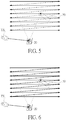
- FIGs. 5-7 are diagrams illustrating the scan method of the 3D sensing system 100 according to embodiments of the present invention.
- a vertical axis and a horizontal axis are defined based on scan timing and scan sequence in the present invention.
- the movement of the MEMS scanning mirror 20 is indicated by arrows, wherein the solid arrows represent the actual scan lines when the light source TX 1 is emitting light and the dotted arrows represent the movement of the MEMS scanning mirror 20 without scanning (the light source TX 1 is off).
- FIG. 5 depicts the embodiment in which a single laser light source TX 1 is used to perform uni-directional scan.
- the MEMS scanning mirror 20 After scanning from the start point to the end point of a current scan line, the MEMS scanning mirror 20 is configured to move from the end point of the current scan line to the start point of a subsequent scan line without scanning (indicated by the dotted arrows) and then resume scanning from the start point to the end point of the subsequent scan line.
- the refresh rate of each frame is 60Hz
- the specific scan plane includes 500 scan lines in the horizontal direction
- FIG.6 depicts the embodiment in which a single laser light source TX 1 is used to perform bi-directional scan.
- the MEMS scanning mirror 20 is configured to continue scanning from the end point of the current scan line to the start point of a subsequent scan line (indicated by the solid arrows).
- the refresh rate of each frame is 60Hz
- the specific scan plane includes 500*2 scan lines in the horizontal direction
- FIG.7 depicts the embodiment in which multiple laser light sources TX 1 ⁇ TX M are used to perform uni-directional scan.
- the light sources TX 1 ⁇ TX 8 may provide light of different pulse width modulations (PWM), wavelengths, frequencies or intensities so that the MEMS scanning mirror 20 can simultaneously scan 8 scan lines.
- PWM pulse width modulations
- FIG. 8 is a functional diagram illustrating a 3D sensing system 200 according to another embodiment of the present invention.
- the 3D sensing system 200 adopts ToF technique and includes one or multiple light modules LG 1 ⁇ LG P , one or multiple sensors SR 1 ⁇ SR N disposed on multiple objects, an MEMS controller 40, and an MCU 50.
- the light modules LG 1 ⁇ LG P each include one or multiple light sources TX 1 ⁇ TX M , one or multiple MEMS scanning mirrors, and a modulation controller, wherein M, N and P are positive integers.
- the light modules LG 1 includes a light source TX 1 , an MEMS scanning mirror 21, and a modulation controller 81 for dynamic tracking a first object 31 on which the sensors SR 1 ⁇ SR 3 are disposed.
- the light modules LG 2 includes a light source TX 2 , an MEMS scanning mirror 22, and a modulation controller 82 for dynamic tracking a second object 32 on which the sensors SR 4 ⁇ SR 6 are disposed.
- the MCU 50 is further configured to synchronize the data captured by each sensor and the activation time of each light source.
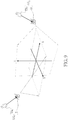
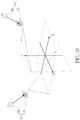
- FIG. 11 is a diagram illustrating the operation of the 3D sensing system 200 according to an embodiment of the present invention.
- the 3D sensing system 200 includes two light modules LG 1 ⁇ LG 2 and six sensors SR 1 ⁇ SR 6 , wherein the first object 31 on which the sensors SR 1 ⁇ SR 3 are disposed is a hand-held control device, and the second object 32 on which the sensors SR 4 ⁇ SR 6 are disposed is a head-mounted display. As depicted in FIGs.
- the MEMS scanning mirror 21 in the light modules LG 1 can reflect the light provided by the light source TX 1 in order to scan the XZ-plane of the object (such as a plane in front of the user), and the MEMS scanning mirror 22 in the light modules LG 2 can reflect the light provided by the light source TX 2 in order to scan the YZ-plane of the object (such as a plane on one lateral side of the user).
- the light sources TX 1 ⁇ TX 2 may provide light of different PWMs, wavelengths, frequencies or intensities so as to be distinguishable to the sensors SR1-SR6.
- the light modules LG 1 and LG 2 may also be used to scan odd/even scan lines in an interleaving manner or in opposite directions for increasing scan accuracy.
- the light sources TX 1 ⁇ TX M may be light emitting diodes (LED) or vertical cavity surface emitting lasers (VCSEL).
- the sensors SR 1 ⁇ SR 2 may be charge coupled devices (CCD) or complementary metal-oxide-semiconductor (CMOS).
- CCD charge coupled devices
- CMOS complementary metal-oxide-semiconductor
- the type of the light sources TX 1 ⁇ TX M or the sensors SR 1 ⁇ SR N does not limit the scope of the present invention.
- the present invention provides a 3D sensing system which adopts TOF technology.
- Multiple MEMS scanning mirrors may be used for scanning, and multiple light sources may be used to detect locations on multiple axes or multiple objects, thereby increasing scan accuracy and reducing scan time.
Landscapes
- Physics & Mathematics (AREA)
- Engineering & Computer Science (AREA)
- Electromagnetism (AREA)
- General Physics & Mathematics (AREA)
- Radar, Positioning & Navigation (AREA)
- Remote Sensing (AREA)
- Computer Networks & Wireless Communication (AREA)
- Multimedia (AREA)
- Signal Processing (AREA)
- Optics & Photonics (AREA)
- Length Measuring Devices By Optical Means (AREA)
- Mechanical Optical Scanning Systems (AREA)
- Measurement Of Optical Distance (AREA)
Applications Claiming Priority (1)
| Application Number | Priority Date | Filing Date | Title |
|---|---|---|---|
| TW107112053A TWI653427B (zh) | 2018-04-09 | 2018-04-09 | 三維感測系統 |
Publications (1)
| Publication Number | Publication Date |
|---|---|
| EP3553555A1 true EP3553555A1 (de) | 2019-10-16 |
Family
ID=62874596
Family Applications (1)
| Application Number | Title | Priority Date | Filing Date |
|---|---|---|---|
| EP18181799.0A Withdrawn EP3553555A1 (de) | 2018-04-09 | 2018-07-05 | 3d-sensorsystem |
Country Status (3)
| Country | Link |
|---|---|
| US (1) | US20190310460A1 (de) |
| EP (1) | EP3553555A1 (de) |
| TW (1) | TWI653427B (de) |
Families Citing this family (1)
| Publication number | Priority date | Publication date | Assignee | Title |
|---|---|---|---|---|
| US10788659B2 (en) * | 2018-10-24 | 2020-09-29 | Infinean Technologies Ag | Monitoring of MEMS mirror properties |
Citations (3)
| Publication number | Priority date | Publication date | Assignee | Title |
|---|---|---|---|---|
| US20050253055A1 (en) * | 2004-05-14 | 2005-11-17 | Microvision, Inc., A Corporation Of The State Of Delaware | MEMS device having simplified drive |
| US20150036105A1 (en) * | 2012-12-26 | 2015-02-05 | Citizen Holdings Co., Ltd. | Projection apparatus |
| CN206362922U (zh) * | 2016-12-14 | 2017-07-28 | 北京国承万通信息科技有限公司 | 定位光信号发射系统及定位系统 |
Family Cites Families (7)
| Publication number | Priority date | Publication date | Assignee | Title |
|---|---|---|---|---|
| US6220713B1 (en) * | 1998-10-23 | 2001-04-24 | Compaq Computer Corporation | Projection lens and system |
| JP5012463B2 (ja) * | 2007-12-03 | 2012-08-29 | セイコーエプソン株式会社 | 走査型画像表示システム及び走査型画像表示装置 |
| TWI345381B (en) | 2007-12-31 | 2011-07-11 | E Pin Optical Industry Co Ltd | Mems scan controller with clock frequency and method of control thereof |
| TW200947164A (en) | 2008-05-09 | 2009-11-16 | E Pin Optical Industry Co Ltd | MEMS scan controller with inherence frequency and method of control thereof |
| CN103857981B (zh) | 2011-10-11 | 2017-05-10 | 株式会社尼康 | 形状测定装置、构造物制造系统、形状测定方法、构造物制造方法 |
| CN103676420B (zh) | 2012-09-04 | 2015-08-19 | 光宝科技股份有限公司 | 具有相位检测及补偿功能的激光扫描式投影装置 |
| EP3093194B1 (de) * | 2015-04-24 | 2021-09-22 | Ricoh Company, Ltd. | Informationsbereitstellungsvorrichtung |
-
2018
- 2018-04-09 TW TW107112053A patent/TWI653427B/zh not_active IP Right Cessation
- 2018-06-14 US US16/008,041 patent/US20190310460A1/en not_active Abandoned
- 2018-07-05 EP EP18181799.0A patent/EP3553555A1/de not_active Withdrawn
Patent Citations (3)
| Publication number | Priority date | Publication date | Assignee | Title |
|---|---|---|---|---|
| US20050253055A1 (en) * | 2004-05-14 | 2005-11-17 | Microvision, Inc., A Corporation Of The State Of Delaware | MEMS device having simplified drive |
| US20150036105A1 (en) * | 2012-12-26 | 2015-02-05 | Citizen Holdings Co., Ltd. | Projection apparatus |
| CN206362922U (zh) * | 2016-12-14 | 2017-07-28 | 北京国承万通信息科技有限公司 | 定位光信号发射系统及定位系统 |
Also Published As
| Publication number | Publication date |
|---|---|
| TW201944028A (zh) | 2019-11-16 |
| US20190310460A1 (en) | 2019-10-10 |
| TWI653427B (zh) | 2019-03-11 |
Similar Documents
| Publication | Publication Date | Title |
|---|---|---|
| US11906726B2 (en) | Micromachined mirror assembly having micro mirror array and hybrid driving method thereof | |
| CN105143820B (zh) | 利用多个发射器进行深度扫描 | |
| CN104160240B (zh) | 扫描深度引擎 | |
| US10598771B2 (en) | Depth sensing with multiple light sources | |
| EP3497926B1 (de) | Vorrichtungen und verfahren zur bereitstellung von tiefenkartierung mit abtastlaser-bildprojektion | |
| EP3685209B1 (de) | Hebelsystem zur steuerung von spiegeln eines lidar-senders | |
| KR20190030228A (ko) | 조정 가능한 해상도 깊이 매핑을 위한 장치 및 방법 | |
| EP3218736A1 (de) | Positionsverfolgungssysteme und -verfahren | |
| US11480660B2 (en) | Arrayed MEMS mirrors for large aperture applications | |
| US20200379092A1 (en) | Steered Lidar System with Arrayed Receiver | |
| US11092679B2 (en) | Compensation for laser light source misalignment in a multiple laser scanning TOF sensor system | |
| US11085995B2 (en) | Non-linear springs to unify the dynamic motion of individual elements in a micro-mirror array | |
| US11061201B2 (en) | Non-linear springs to unify the dynamic motion of individual elements in a micro-mirror array | |
| EP3553555A1 (de) | 3d-sensorsystem | |
| US10642025B2 (en) | Method for controlling position of a linear MEMS mirror with variable resolution and/or light intensity | |
| CN115015961B (zh) | 利用李萨如扫描的矩形2d图案生成的方法 | |
| KR102473423B1 (ko) | Tof 카메라 장치 | |
| JP2015040928A (ja) | 光偏向装置、画像形成装置、車両及び光偏向装置の制御方法 | |
| US20230314790A1 (en) | System-level synchronization of microelectromechanical system (mems) mirrors | |
| CN106415361A (zh) | 用于装有万向接头的扫描镜阵列的耦接方案 | |
| CN110412597A (zh) | 三维感测系统 | |
| WO2023048691A1 (en) | Fast and high-resolution lidar with multiaxis and multi- surface polygon scanner | |
| US20190391265A1 (en) | 3d sensing system | |
| US12461358B2 (en) | Piezoelectric micro mirror with corrugated actuator and suspension system | |
| US20250355094A1 (en) | Scanning profiles with intra-scan temporal optimization for lidar sensing |
Legal Events
| Date | Code | Title | Description |
|---|---|---|---|
| PUAI | Public reference made under article 153(3) epc to a published international application that has entered the european phase |
Free format text: ORIGINAL CODE: 0009012 |
|
| STAA | Information on the status of an ep patent application or granted ep patent |
Free format text: STATUS: THE APPLICATION HAS BEEN PUBLISHED |
|
| AK | Designated contracting states |
Kind code of ref document: A1 Designated state(s): AL AT BE BG CH CY CZ DE DK EE ES FI FR GB GR HR HU IE IS IT LI LT LU LV MC MK MT NL NO PL PT RO RS SE SI SK SM TR |
|
| AX | Request for extension of the european patent |
Extension state: BA ME |
|
| STAA | Information on the status of an ep patent application or granted ep patent |
Free format text: STATUS: THE APPLICATION IS DEEMED TO BE WITHDRAWN |
|
| 18D | Application deemed to be withdrawn |
Effective date: 20200603 |