EP3551986B1 - Led light source probe card technology for testing cmos image scan devices - Google Patents
Led light source probe card technology for testing cmos image scan devices Download PDFInfo
- Publication number
- EP3551986B1 EP3551986B1 EP17879336.0A EP17879336A EP3551986B1 EP 3551986 B1 EP3551986 B1 EP 3551986B1 EP 17879336 A EP17879336 A EP 17879336A EP 3551986 B1 EP3551986 B1 EP 3551986B1
- Authority
- EP
- European Patent Office
- Prior art keywords
- led light
- light source
- led
- uniformity
- photodetector
- Prior art date
- Legal status (The legal status is an assumption and is not a legal conclusion. Google has not performed a legal analysis and makes no representation as to the accuracy of the status listed.)
- Active
Links
Images

Classifications
-
- G—PHYSICS
- G01—MEASURING; TESTING
- G01N—INVESTIGATING OR ANALYSING MATERIALS BY DETERMINING THEIR CHEMICAL OR PHYSICAL PROPERTIES
- G01N21/00—Investigating or analysing materials by the use of optical means, i.e. using sub-millimetre waves, infrared, visible or ultraviolet light
- G01N21/84—Systems specially adapted for particular applications
- G01N21/88—Investigating the presence of flaws or contamination
- G01N21/8806—Specially adapted optical and illumination features
-
- G—PHYSICS
- G01—MEASURING; TESTING
- G01J—MEASUREMENT OF INTENSITY, VELOCITY, SPECTRAL CONTENT, POLARISATION, PHASE OR PULSE CHARACTERISTICS OF INFRARED, VISIBLE OR ULTRAVIOLET LIGHT; COLORIMETRY; RADIATION PYROMETRY
- G01J1/00—Photometry, e.g. photographic exposure meter
- G01J1/02—Details
- G01J1/04—Optical or mechanical part supplementary adjustable parts
- G01J1/0407—Optical elements not provided otherwise, e.g. manifolds, windows, holograms, gratings
- G01J1/0418—Optical elements not provided otherwise, e.g. manifolds, windows, holograms, gratings using attenuators
-
- G—PHYSICS
- G01—MEASURING; TESTING
- G01J—MEASUREMENT OF INTENSITY, VELOCITY, SPECTRAL CONTENT, POLARISATION, PHASE OR PULSE CHARACTERISTICS OF INFRARED, VISIBLE OR ULTRAVIOLET LIGHT; COLORIMETRY; RADIATION PYROMETRY
- G01J1/00—Photometry, e.g. photographic exposure meter
- G01J1/02—Details
- G01J1/08—Arrangements of light sources specially adapted for photometry standard sources, also using luminescent or radioactive material
-
- G—PHYSICS
- G01—MEASURING; TESTING
- G01J—MEASUREMENT OF INTENSITY, VELOCITY, SPECTRAL CONTENT, POLARISATION, PHASE OR PULSE CHARACTERISTICS OF INFRARED, VISIBLE OR ULTRAVIOLET LIGHT; COLORIMETRY; RADIATION PYROMETRY
- G01J1/00—Photometry, e.g. photographic exposure meter
- G01J1/10—Photometry, e.g. photographic exposure meter by comparison with reference light or electric value provisionally void
- G01J1/20—Photometry, e.g. photographic exposure meter by comparison with reference light or electric value provisionally void intensity of the measured or reference value being varied to equalise their effects at the detectors, e.g. by varying incidence angle
- G01J1/28—Photometry, e.g. photographic exposure meter by comparison with reference light or electric value provisionally void intensity of the measured or reference value being varied to equalise their effects at the detectors, e.g. by varying incidence angle using variation of intensity or distance of source
- G01J1/30—Photometry, e.g. photographic exposure meter by comparison with reference light or electric value provisionally void intensity of the measured or reference value being varied to equalise their effects at the detectors, e.g. by varying incidence angle using variation of intensity or distance of source using electric radiation detectors
- G01J1/32—Photometry, e.g. photographic exposure meter by comparison with reference light or electric value provisionally void intensity of the measured or reference value being varied to equalise their effects at the detectors, e.g. by varying incidence angle using variation of intensity or distance of source using electric radiation detectors adapted for automatic variation of the measured or reference value
-
- G—PHYSICS
- G01—MEASURING; TESTING
- G01J—MEASUREMENT OF INTENSITY, VELOCITY, SPECTRAL CONTENT, POLARISATION, PHASE OR PULSE CHARACTERISTICS OF INFRARED, VISIBLE OR ULTRAVIOLET LIGHT; COLORIMETRY; RADIATION PYROMETRY
- G01J1/00—Photometry, e.g. photographic exposure meter
- G01J1/42—Photometry, e.g. photographic exposure meter using electric radiation detectors
-
- G—PHYSICS
- G01—MEASURING; TESTING
- G01N—INVESTIGATING OR ANALYSING MATERIALS BY DETERMINING THEIR CHEMICAL OR PHYSICAL PROPERTIES
- G01N21/00—Investigating or analysing materials by the use of optical means, i.e. using sub-millimetre waves, infrared, visible or ultraviolet light
- G01N21/84—Systems specially adapted for particular applications
- G01N21/88—Investigating the presence of flaws or contamination
-
- G—PHYSICS
- G01—MEASURING; TESTING
- G01R—MEASURING ELECTRIC VARIABLES; MEASURING MAGNETIC VARIABLES
- G01R31/00—Arrangements for testing electric properties; Arrangements for locating electric faults; Arrangements for electrical testing characterised by what is being tested not provided for elsewhere
- G01R31/28—Testing of electronic circuits, e.g. by signal tracer
- G01R31/2851—Testing of integrated circuits [IC]
- G01R31/2886—Features relating to contacting the IC under test, e.g. probe heads; chucks
- G01R31/2889—Interfaces, e.g. between probe and tester
-
- G—PHYSICS
- G01—MEASURING; TESTING
- G01R—MEASURING ELECTRIC VARIABLES; MEASURING MAGNETIC VARIABLES
- G01R31/00—Arrangements for testing electric properties; Arrangements for locating electric faults; Arrangements for electrical testing characterised by what is being tested not provided for elsewhere
- G01R31/28—Testing of electronic circuits, e.g. by signal tracer
- G01R31/302—Contactless testing
- G01R31/308—Contactless testing using non-ionising electromagnetic radiation, e.g. optical radiation
- G01R31/311—Contactless testing using non-ionising electromagnetic radiation, e.g. optical radiation of integrated circuits
-
- G—PHYSICS
- G02—OPTICS
- G02B—OPTICAL ELEMENTS, SYSTEMS OR APPARATUS
- G02B27/00—Optical systems or apparatus not provided for by any of the groups G02B1/00 - G02B26/00, G02B30/00
- G02B27/09—Beam shaping, e.g. changing the cross-sectional area, not otherwise provided for
- G02B27/0938—Using specific optical elements
- G02B27/095—Refractive optical elements
- G02B27/0955—Lenses
-
- H—ELECTRICITY
- H04—ELECTRIC COMMUNICATION TECHNIQUE
- H04N—PICTORIAL COMMUNICATION, e.g. TELEVISION
- H04N1/00—Scanning, transmission or reproduction of documents or the like, e.g. facsimile transmission; Details thereof
- H04N1/024—Details of scanning heads ; Means for illuminating the original
- H04N1/028—Details of scanning heads ; Means for illuminating the original for picture information pick-up
- H04N1/02815—Means for illuminating the original, not specific to a particular type of pick-up head
- H04N1/0288—Means for illuminating the original, not specific to a particular type of pick-up head using a two-dimensional light source, e.g. two-dimensional LED array
-
- H—ELECTRICITY
- H04—ELECTRIC COMMUNICATION TECHNIQUE
- H04N—PICTORIAL COMMUNICATION, e.g. TELEVISION
- H04N1/00—Scanning, transmission or reproduction of documents or the like, e.g. facsimile transmission; Details thereof
- H04N1/024—Details of scanning heads ; Means for illuminating the original
- H04N1/028—Details of scanning heads ; Means for illuminating the original for picture information pick-up
- H04N1/02815—Means for illuminating the original, not specific to a particular type of pick-up head
- H04N1/02885—Means for compensating spatially uneven illumination, e.g. an aperture arrangement
-
- H—ELECTRICITY
- H04—ELECTRIC COMMUNICATION TECHNIQUE
- H04N—PICTORIAL COMMUNICATION, e.g. TELEVISION
- H04N17/00—Diagnosis, testing or measuring for television systems or their details
- H04N17/002—Diagnosis, testing or measuring for television systems or their details for television cameras
-
- G—PHYSICS
- G01—MEASURING; TESTING
- G01J—MEASUREMENT OF INTENSITY, VELOCITY, SPECTRAL CONTENT, POLARISATION, PHASE OR PULSE CHARACTERISTICS OF INFRARED, VISIBLE OR ULTRAVIOLET LIGHT; COLORIMETRY; RADIATION PYROMETRY
- G01J1/00—Photometry, e.g. photographic exposure meter
- G01J1/42—Photometry, e.g. photographic exposure meter using electric radiation detectors
- G01J2001/4247—Photometry, e.g. photographic exposure meter using electric radiation detectors for testing lamps or other light sources
- G01J2001/4252—Photometry, e.g. photographic exposure meter using electric radiation detectors for testing lamps or other light sources for testing LED's
-
- G—PHYSICS
- G01—MEASURING; TESTING
- G01R—MEASURING ELECTRIC VARIABLES; MEASURING MAGNETIC VARIABLES
- G01R31/00—Arrangements for testing electric properties; Arrangements for locating electric faults; Arrangements for electrical testing characterised by what is being tested not provided for elsewhere
- G01R31/28—Testing of electronic circuits, e.g. by signal tracer
- G01R31/282—Testing of electronic circuits specially adapted for particular applications not provided for elsewhere
- G01R31/2831—Testing of materials or semi-finished products, e.g. semiconductor wafers or substrates
Definitions
- This invention relates to probing and testing of optoelectronic devices, especially CMOS image scan (CIS) devices.
- optoelectronic devices especially CMOS image scan (CIS) devices.
- CMOS complementary metal-oxide-silicon
- CMOS complementary metal-oxide-silicon
- This arrangement has significant disadvantages, including large size, significant required maintenance and difficulty in reconfiguring test setups. These problems become especially acute in the context of wafer-scale device testing, where a light source having a diameter as high as 300 mm may be required. Accordingly, it would be an advance in the art to provide an improved light source/probe card for testing optoelectronic devices.
- US 2007/159190 discloses an optical test apparatus, related test method and method of operation, and related probe card adapted to optically test an image sensor.
- An illumination source of the optical test apparatus provides an optical test signal to the image sensor through the probe card.
- the optical test signal has a property variably defined by a feedback loop formed between a reference image sensor associated with the probe card and a control unit connected between the reference image sensor and the illumination source.
- KR 2008 0041792 relates to an apparatus for testing an image sensor is provided to selectively test the required number of chips and to improve test reliability by controlling a region of light incident into the image sensor according to the number of the chips for testing.
- a light source irradiates light to an image sensor.
- a diffusion filter is arranged between the light source and the image sensor. The diffusion filter controls an angle of the light incident into the image sensor.
- a probe card has a probe contacted to a pad of the image sensor. The probe card tests photoelectric transformation characteristic of the image sensor according to the light.
- a support supports a side of the diffusion filter. The support fixes the diffusion filter to the probe card.
- a fly-eye lens array is formed between the light source and the diffusion filter. The fly-eye lens array makes intensity of the light irradiated from the light source uniform.
- US 2006/237636 relates to a system to provide visible lighting of a selectable spectral characteristic (e.g. a selectable color combination of light) uses an optical integrating cavity or other diffuse mixing element to combine light of different colors from different color LEDs.
- Amplitude modulation of pulsed operation the light sources, e.g. pulse amplitude modulation added to a baseline forward bias current for each of the LEDs, controls the amount of each light color supplied to the diffuse mixing element and thus the amount included in the combined light output of the system.
- a color sensor may provide feedback as to a color characteristic of the combined light, for closed-loop control of one or more of the pulse amplitude modulations. Examples are also disclosed that utilize phosphor doping of one or more of the system's reflective elements, to add desired wavelengths of light to the combined output.
- JP 2009 105262 discloses an inspection device, for each of at least two solid-state imaging elements: probes each electrically connected to a signal terminal of each solid-state imaging element; a shielding structure covering at least a light reception part of each solid-state imaging element; and a light source arranged inside the shielding structures.
- the inspection device can emit, to the plurality of solid-state imaging elements, stable light rays at the same time.
- the basic architecture is an LED array having one LED source per CIS device chip being tested. Arrays of LEDs are used because such testing is typically done wafer-scale, as opposed to being performed individually for single devices.
- the LEDs illuminate a phosphor which provides the light used for testing.
- An aperture + lens arrangement is used to provide telecentric light. In some embodiments, the aperture can be used as part of the cooling arrangement for the LEDs.
- Uniformity filters can be used to improve illumination uniformity within a chip and/or from one chip to the next. Such filters can be regarded as pixelated neutral density filters. Operation under closed loop control can be used to correct for device to device variation among the LEDs. In one example, such control makes use of two calibration tables, one for high illuminance (i.e., over 100 lx) and low illuminance (i.e., 100 lx or less). Another feature of the feedback control, according to the present invention, is the use of two photodetectors, one photodetector having a neutral density filter on it, and the other photodetector not having a neutral density filter on it.
- Feedback control of LED intensity can make use of two feedback paths: 1) LED to photodetector and 2) LED to phosphor to photodetector. Feedback control can also be done with a single photodetector in the LED light source module, either with or without a neutral density filter on the photodetector. However, this option does not fall within the scope of the claims.
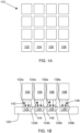
- FIGs. 1A-B show an exemplary embodiment of the invention.
- FIG. 1A is a top view
- FIG. 1B is a corresponding side view of apparatus for testing an array of light-sensitive electronic devices.
- FIG. 1A shows an array of LED (light emitting diode) light sources 110, four of which are referenced as 102, 104, 106, and 108.
- the array of sources need not be square as shown on FIG. 1A .
- gaps may be placed between the LED light sources so that the arrangement is not contiguous.
- array 110 is configured to have an LED light source corresponding to each of the electronic devices under test.
- sources 102, 104, 106, 108 correspond to devices under test 122, 124, 126, 128, respectively. More specifically, sources 102, 104, 106, 108 provide output light 142, 144, 146, 148 to devices under test 122, 124, 126, 128, respectively.
- devices under test 122, 124, 126, 128 are schematically shown as being disposed in substrate 120, which would be the case for wafer scale testing.
- an important advantage of the present approach is that the small size of the LED light sources simplifies integration of optical illumination and electrical probing to provide a true optoelectronic probe card for testing optoelectronic imaging devices.
- this preferred feature is shown by electrical probes 132a,b, 134a,b, 136a,b, 138a,b which make electrical contact to electrical terminals of devices under test 122, 124, 126, 128, respectively.
- two electrical probes per device under test are shown, but in practice any number of electrical probes can be used per device under test.
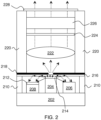
- FIG. 2 is a detailed view of an exemplary LED source suitable for use in embodiments of the invention.
- light emitting diode 214 provides LED light (solid arrows), and a phosphor 216 is disposed to receive the LED light and to provide phosphorescence light (dashed arrows).
- An aperture 218 is configured to provide point source illumination from the phosphorescence light, as shown.
- a lens 222 is configured to provide collimated light from the point source illumination. Lens 222 is preferably an aspheric lens designed for this collimation function over the wavelength range provided by phosphor 216.
- a uniformity filter 228 is disposed to receive the collimated light and to provide output light having improved uniformity of illumination.
- FIG. 2 also shows further features that are present in preferred embodiments and/or in complete designs.
- LED 214 is mounted on a heat sink member 204, and the package includes a first photodiode 206, a second photodiode 208, and a neutral density filter 212 disposed on the second photodiode.
- these photodiodes are used in preferred embodiments to provide signals for feedback control of the array of LED light sources.
- Heat sink 204 and photodiodes 206 and 208 are disposed on substrate 202.
- Spacer members 210 are used to support the phosphor 216 and aperture 218 at the appropriate vertical height.
- a lens housing 220 positions lens 222 at the correct distance from aperture 218 to provide collimated (i.e., telecentric) light as shown.
- Optional components that can be disposed in the path of the collimated light include infra-red (IR) filter 224 and/or diffuser 226.
- IR filter blocks IR radiation from reaching devices under test to provide purely visible light to the device under test, and the diffuser helps improve the uniformity of light provided by the light source to the device under test.
- the first photodetector 206 and the second photodetector 208 will typically receive light within the LED light source from both LED 214 (solid arrows) and phosphor 216 (dashed arrows).
- the phosphor for each LED light source is preferably configured as a thin film of uniform thickness disposed on the light emitting diode of the LED light source, as shown on FIG. 2 .
- phosphor 216 is a mixture of phosphors chosen to provide substantially white illumination (e.g., by combining red, green and blue emitting phosphors).
- the phosphor or phosphor mixture can be selected to emphasize a particular desired spectral distribution.
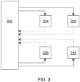
- FIG. 3 shows a control approach suitable for use in embodiments of the invention.
- a feedback control system 302 receives measured optical signals (dotted lines) from each LED light source 304, 306, 308, 310 and is configured to control operation (solid lines) of the array of LED light sources using the measured optical signals to provide uniform illumination to the array of light-sensitive electronic devices.
- a calibration of the system can be performed to relate measured optical signals to emitted light intensity for each LED light source.
- This data can then be used to create a lookup table in control system 302 such that each LED light source is driven so that its measured optical signals are in accordance with the lookup table for the desired array intensity. Interpolation in the lookup table can be performed for desired intensity values that are intermediate between calibration data points. Such calibration can be done initially and then repeated occasionally if or as needed to account for drift in device performance over time. For ease of illustration, only four LED light sources are shown in the example of FIG. 3 , but such feedback control can be practiced for arrays having any number of LED light sources.
- two feedback signals are used from each LED light source, a first signal from a first photodetector that has no neutral density filter disposed on it, and a second signal from a second photodetector that has a neutral density filter disposed on it.
- the purpose of having two detectors for feedback configured this way is to improve dynamic range because a single detector can only provide useful feedback over a limited range of optical intensity. So in this example, second detector 208 will be able to provide useful feedback when the optical intensity is high enough to saturate first detector 206 because of neutral density filter 212.
- neutral density filter 212 is configured to provide a continuous feedback range for the two detectors combined (e.g., signal from detector 208 is at 1% of its saturation value for the lowest optical intensity that saturates detector 206). Additional feedback detectors plus neutral density filters can be added to further increase dynamic range according to these principles if necessary. Alternatively, however, not falling within the scope of the appended claims, a single detector (with or without a neutral density filter on it) can be used to provide the optical signals for feedback.
- Uniformity is also improved by making use of uniformity filters 228 in each LED light source.
- These uniformity filters can be neutral density filters individually customized for their corresponding LED light sources according to calibration measurements of output light uniformity of the array of LED light sources prior to installation of the uniformity filter.
- uniformity from one LED light source to another is provided using both active measures (feedback control) and passive measures (the uniformity filters) in combination.
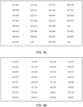
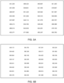
- FIGs. 4A-B show first exemplary experimental results for array uniformity.
- FIG. 4A is a table of emission values from an LED array with all drive currents being the same, and FIG. 4B is from the same array after installation of suitable customized uniformity filters for each source in the array.
- the emission values have a maximum of 555, a minimum of 463, an average of 520 and a standard deviation of 22.
- the emission values have a maximum of 553, a minimum of 546, an average of 550, and a standard deviation of 1.9.
- the array of FIG. 4B provide much more uniform illumination than the array of FIG. 4A , and closed loop control can be expected to further improve illumination uniformity from one LED light source to another.
- FIGs. 5A-B show second exemplary experimental results for array uniformity.
- FIGs. 4A-B are results for one tester type with the apparatus, and FIGs. 5A-B are results for another tester type with the same or similar apparatus.
- FIG. 5A is a table of emission values from an LED array with all drive currents being the same, and FIG. 5B is from the same array after installation of suitable customized uniformity filters for each source in the array.
- the emission values have a maximum of 551, a minimum of 451, an average of 506 and a standard deviation of 32.
- the emission values have a maximum of 564, a minimum of 554, an average of 559, and a standard deviation of 2.3.
- the array of FIG. 5B provide much more uniform illumination than the array of FIG. 5A , and closed loop control can be expected to further improve illumination uniformity from one LED light source to another.
- LED source arrays as in the examples of FIGs. 4A-B and 5A-B have been compared to conventional halogen light sources for testing applications, and the LED source arrays provide comparably uniform illumination to the conventional halogen light sources.
- the preceding examples show how uniformity filters can be used to improve uniformity from one device under test to another. It is also possible to use the uniformity filters to improve uniformity of illumination from each LED light source, alternatively to or in addition to improving uniformity between LED light sources.
- FIGs. 6A-C schematically show how uniformity within a single LED source can be improved.
- FIG. 6A schematically shows a light emission pattern that one might obtain from an LED source as described above.
- a uniformity filter can be tailored to have transmission as shown on FIG. 6B (i.e., less transmission for the more intense parts of the beam pattern of FIG. 6A , and more transmission for the less intense parts of the beam pattern of FIG. 6A ).
- Photolithography e.g., chrome on glass or quartz
- the uniformity filter for each LED light source is individually customized for its corresponding LED light source according to calibration measurements of output light uniformity of its corresponding LED light source prior to installation of the uniformity filter.
Landscapes
- Engineering & Computer Science (AREA)
- Physics & Mathematics (AREA)
- General Physics & Mathematics (AREA)
- Multimedia (AREA)
- Signal Processing (AREA)
- Spectroscopy & Molecular Physics (AREA)
- General Engineering & Computer Science (AREA)
- Health & Medical Sciences (AREA)
- Microelectronics & Electronic Packaging (AREA)
- Computer Hardware Design (AREA)
- General Health & Medical Sciences (AREA)
- Analytical Chemistry (AREA)
- Pathology (AREA)
- Immunology (AREA)
- Biochemistry (AREA)
- Chemical & Material Sciences (AREA)
- Life Sciences & Earth Sciences (AREA)
- Toxicology (AREA)
- Computer Vision & Pattern Recognition (AREA)
- Electromagnetism (AREA)
- Optics & Photonics (AREA)
- Biomedical Technology (AREA)
- Testing Or Measuring Of Semiconductors Or The Like (AREA)
- Testing Of Optical Devices Or Fibers (AREA)
- Testing Of Individual Semiconductor Devices (AREA)
- Optical Filters (AREA)
- Solid State Image Pick-Up Elements (AREA)
- Led Device Packages (AREA)
- Measuring Leads Or Probes (AREA)
Description
- This invention relates to probing and testing of optoelectronic devices, especially CMOS image scan (CIS) devices.
- Conventional testing of CMOS (complementary metal-oxide-silicon) image scan devices makes use of a halogen lamp to provide light for testing. This arrangement has significant disadvantages, including large size, significant required maintenance and difficulty in reconfiguring test setups. These problems become especially acute in the context of wafer-scale device testing, where a light source having a diameter as high as 300 mm may be required. Accordingly, it would be an advance in the art to provide an improved light source/probe card for testing optoelectronic devices.
-
US 2007/159190 discloses an optical test apparatus, related test method and method of operation, and related probe card adapted to optically test an image sensor. An illumination source of the optical test apparatus provides an optical test signal to the image sensor through the probe card. The optical test signal has a property variably defined by a feedback loop formed between a reference image sensor associated with the probe card and a control unit connected between the reference image sensor and the illumination source. -
KR 2008 0041792 -
US 2006/237636 relates to a system to provide visible lighting of a selectable spectral characteristic (e.g. a selectable color combination of light) uses an optical integrating cavity or other diffuse mixing element to combine light of different colors from different color LEDs. Amplitude modulation of pulsed operation the light sources, e.g. pulse amplitude modulation added to a baseline forward bias current for each of the LEDs, controls the amount of each light color supplied to the diffuse mixing element and thus the amount included in the combined light output of the system. A color sensor may provide feedback as to a color characteristic of the combined light, for closed-loop control of one or more of the pulse amplitude modulations. Examples are also disclosed that utilize phosphor doping of one or more of the system's reflective elements, to add desired wavelengths of light to the combined output. -
JP 2009 105262 - The present invention is defined in appended independent claim 1 to which reference should be made. Advantageous features are set out in the appended dependent claims.
- We provide a solution to the above-described problems based on the use of light emitting diodes (LEDs) as the light source for CIS device testing. The basic architecture is an LED array having one LED source per CIS device chip being tested. Arrays of LEDs are used because such testing is typically done wafer-scale, as opposed to being performed individually for single devices. The LEDs illuminate a phosphor which provides the light used for testing. An aperture + lens arrangement is used to provide telecentric light. In some embodiments, the aperture can be used as part of the cooling arrangement for the LEDs.
- Uniformity filters can be used to improve illumination uniformity within a chip and/or from one chip to the next. Such filters can be regarded as pixelated neutral density filters. Operation under closed loop control can be used to correct for device to device variation among the LEDs. In one example, such control makes use of two calibration tables, one for high illuminance (i.e., over 100 lx) and low illuminance (i.e., 100 lx or less). Another feature of the feedback control, according to the present invention, is the use of two photodetectors, one photodetector having a neutral density filter on it, and the other photodetector not having a neutral density filter on it. Feedback control of LED intensity can make use of two feedback paths: 1) LED to photodetector and 2) LED to phosphor to photodetector. Feedback control can also be done with a single photodetector in the LED light source module, either with or without a neutral density filter on the photodetector. However, this option does not fall within the scope of the claims.
-
-
FIGs. 1A-B show an embodiment of the invention. -
FIG. 2 is a detailed view of an LED source suitable for use in embodiments of the invention. -
FIG. 3 shows a control approach suitable for use in embodiments of the invention. -
FIGs. 4A-B show first exemplary experimental results for array uniformity. -
FIGs. 5A-B show second exemplary experimental results for array uniformity. -
FIGs. 6A-C schematically show how uniformity from a single LED source can be improved. -
FIGs. 1A-B show an exemplary embodiment of the invention. HereFIG. 1A is a top view andFIG. 1B is a corresponding side view of apparatus for testing an array of light-sensitive electronic devices.FIG. 1A shows an array of LED (light emitting diode)light sources 110, four of which are referenced as 102, 104, 106, and 108. The array of sources need not be square as shown onFIG. 1A . Another possible variation is that gaps may be placed between the LED light sources so that the arrangement is not contiguous. - As shown in the side view of
FIG. 1B ,array 110 is configured to have an LED light source corresponding to each of the electronic devices under test. In this example,sources test sources output light test test substrate 120, which would be the case for wafer scale testing. - An important advantage of the present approach is that the small size of the LED light sources simplifies integration of optical illumination and electrical probing to provide a true optoelectronic probe card for testing optoelectronic imaging devices. In the example of
FIGs. 1A-B , this preferred feature is shown byelectrical probes 132a,b, 134a,b, 136a,b, 138a,b which make electrical contact to electrical terminals of devices undertest -
FIG. 2 is a detailed view of an exemplary LED source suitable for use in embodiments of the invention. In this example of a preferred embodiment,light emitting diode 214 provides LED light (solid arrows), and aphosphor 216 is disposed to receive the LED light and to provide phosphorescence light (dashed arrows). Anaperture 218 is configured to provide point source illumination from the phosphorescence light, as shown. Alens 222 is configured to provide collimated light from the point source illumination.Lens 222 is preferably an aspheric lens designed for this collimation function over the wavelength range provided byphosphor 216. Auniformity filter 228 is disposed to receive the collimated light and to provide output light having improved uniformity of illumination. - The example of
FIG. 2 also shows further features that are present in preferred embodiments and/or in complete designs. HereLED 214 is mounted on aheat sink member 204, and the package includes afirst photodiode 206, asecond photodiode 208, and aneutral density filter 212 disposed on the second photodiode. As explained in more detail below, these photodiodes are used in preferred embodiments to provide signals for feedback control of the array of LED light sources.Heat sink 204 andphotodiodes substrate 202.Spacer members 210 are used to support thephosphor 216 andaperture 218 at the appropriate vertical height. Alens housing 220positions lens 222 at the correct distance fromaperture 218 to provide collimated (i.e., telecentric) light as shown. Optional components that can be disposed in the path of the collimated light include infra-red (IR)filter 224 and/ordiffuser 226. Here the IR filter blocks IR radiation from reaching devices under test to provide purely visible light to the device under test, and the diffuser helps improve the uniformity of light provided by the light source to the device under test. - As shown on
FIG. 2 thefirst photodetector 206 and thesecond photodetector 208 will typically receive light within the LED light source from both LED 214 (solid arrows) and phosphor 216 (dashed arrows). The phosphor for each LED light source is preferably configured as a thin film of uniform thickness disposed on the light emitting diode of the LED light source, as shown onFIG. 2 . Preferablyphosphor 216 is a mixture of phosphors chosen to provide substantially white illumination (e.g., by combining red, green and blue emitting phosphors). Alternatively, the phosphor or phosphor mixture can be selected to emphasize a particular desired spectral distribution. - An important aspect of preferred embodiments of the invention is feedback control of each LED light source in the emitting array, to provide uniformity of illumination to all devices under test.
FIG. 3 shows a control approach suitable for use in embodiments of the invention. Here afeedback control system 302 receives measured optical signals (dotted lines) from eachLED light source control system 302 such that each LED light source is driven so that its measured optical signals are in accordance with the lookup table for the desired array intensity. Interpolation in the lookup table can be performed for desired intensity values that are intermediate between calibration data points. Such calibration can be done initially and then repeated occasionally if or as needed to account for drift in device performance over time. For ease of illustration, only four LED light sources are shown in the example ofFIG. 3 , but such feedback control can be practiced for arrays having any number of LED light sources. - In preferred embodiments like the example of
FIG. 2 , two feedback signals are used from each LED light source, a first signal from a first photodetector that has no neutral density filter disposed on it, and a second signal from a second photodetector that has a neutral density filter disposed on it. The purpose of having two detectors for feedback configured this way is to improve dynamic range because a single detector can only provide useful feedback over a limited range of optical intensity. So in this example,second detector 208 will be able to provide useful feedback when the optical intensity is high enough to saturatefirst detector 206 because ofneutral density filter 212. Preferablyneutral density filter 212 is configured to provide a continuous feedback range for the two detectors combined (e.g., signal fromdetector 208 is at 1% of its saturation value for the lowest optical intensity that saturates detector 206). Additional feedback detectors plus neutral density filters can be added to further increase dynamic range according to these principles if necessary. Alternatively, however, not falling within the scope of the appended claims, a single detector (with or without a neutral density filter on it) can be used to provide the optical signals for feedback. - Uniformity is also improved by making use of uniformity filters 228 in each LED light source. These uniformity filters can be neutral density filters individually customized for their corresponding LED light sources according to calibration measurements of output light uniformity of the array of LED light sources prior to installation of the uniformity filter. In other words, uniformity from one LED light source to another is provided using both active measures (feedback control) and passive measures (the uniformity filters) in combination.
-
FIGs. 4A-B show first exemplary experimental results for array uniformity. HereFIG. 4A is a table of emission values from an LED array with all drive currents being the same, andFIG. 4B is from the same array after installation of suitable customized uniformity filters for each source in the array. InFIG. 4A , the emission values have a maximum of 555, a minimum of 463, an average of 520 and a standard deviation of 22. InFIG. 4B , the emission values have a maximum of 553, a minimum of 546, an average of 550, and a standard deviation of 1.9. Clearly the array ofFIG. 4B provide much more uniform illumination than the array ofFIG. 4A , and closed loop control can be expected to further improve illumination uniformity from one LED light source to another. -
FIGs. 5A-B show second exemplary experimental results for array uniformity.FIGs. 4A-B are results for one tester type with the apparatus, andFIGs. 5A-B are results for another tester type with the same or similar apparatus. HereFIG. 5A is a table of emission values from an LED array with all drive currents being the same, andFIG. 5B is from the same array after installation of suitable customized uniformity filters for each source in the array. InFIG. 5A , the emission values have a maximum of 551, a minimum of 451, an average of 506 and a standard deviation of 32. InFIG. 5B , the emission values have a maximum of 564, a minimum of 554, an average of 559, and a standard deviation of 2.3. Clearly the array ofFIG. 5B provide much more uniform illumination than the array ofFIG. 5A , and closed loop control can be expected to further improve illumination uniformity from one LED light source to another. - LED source arrays as in the examples of
FIGs. 4A-B and5A-B have been compared to conventional halogen light sources for testing applications, and the LED source arrays provide comparably uniform illumination to the conventional halogen light sources. - The preceding examples show how uniformity filters can be used to improve uniformity from one device under test to another. It is also possible to use the uniformity filters to improve uniformity of illumination from each LED light source, alternatively to or in addition to improving uniformity between LED light sources.
-
FIGs. 6A-C schematically show how uniformity within a single LED source can be improved. HereFIG. 6A schematically shows a light emission pattern that one might obtain from an LED source as described above. A uniformity filter can be tailored to have transmission as shown onFIG. 6B (i.e., less transmission for the more intense parts of the beam pattern ofFIG. 6A , and more transmission for the less intense parts of the beam pattern ofFIG. 6A ). Photolithography (e.g., chrome on glass or quartz) or the like can be used to make a filter having such variable transmission. Once installed, the resulting intensity distribution should be more uniform, as schematically shown onFIG. 6C . Here the uniformity filter for each LED light source is individually customized for its corresponding LED light source according to calibration measurements of output light uniformity of its corresponding LED light source prior to installation of the uniformity filter.
Claims (9)
- Apparatus for testing an array of light-sensitive electronic devices, the apparatus comprising:an array of LED, light emitting diode, light sources, wherein the array of LED light sources (110) is configured to have a respective LED light source (102, 104, 106, 108) corresponding to each of the electronic devices (122, 124, 126, 128);wherein each LED light source (102, 104, 106, 108) includes a light emitting diode configured to provide LED light;wherein each LED light source (102, 104, 106, 108) includes a phosphor (216) disposed to receive the LED light and to provide phosphorescence light;wherein each LED light source (102, 104, 106, 108) includes an aperture (218) configured to provide point source illumination from the phosphorescence light;wherein each LED light source (102, 104, 106, 108) includes a lens configured to provide collimated light from the point source illumination;wherein each LED light source (102, 104, 106, 108) includes a uniformity filter disposed to receive the collimated light and to provide output light having improved uniformity of illumination;a feedback control system configured to measure optical signals from each LED light source (102, 104, 106, 108) and configured to control operation of the array of LED light sources (102, 104, 106, 108) using the measured optical signals to provide uniform illumination to the array of light-sensitive electronic devices(122, 124, 126, 128) ;wherein each LED light source further comprises a first photodetector and a second photodetector with a neutral density filter disposed on the second photodetector;wherein the optical signals are provided by both the first photodetector and the second photodetector.
- The apparatus of claim 1,wherein the apparatus is a probe card for testing optoelectronic imaging devices, andwherein the probe card further comprises one or more electrical probes (132a,b, 134a,b, 136a,b, 138a,b) for making electrical contact to electrical terminals of optoelectronic imaging devices under test.
- The apparatus of claim 1, wherein the phosphor (216) for each LED light source (102, 104, 106, 108) is configured as a thin film of uniform thickness disposed on the light emitting diode of the LED light source (102, 104, 106, 108) .
- The apparatus of claim 1, wherein the feedback control system is configured to make use of a lookup table derived from calibration measurements of output light from the LED light sources (102, 104, 106, 108).
- The apparatus of claim 1, further comprising a neutral density filter disposed on the first photodetector.
- The apparatus of claim 1, wherein the first photodetector is configured to receive light within the LED light source (102, 104, 106, 108) from both the LED and the phosphor of the LED light source.
- The apparatus of claim 1, wherein the first photodetector and the second photodetector are configured to receive light within the LED light source (102, 104, 106, 108) from both the LED and the phosphor of the LED light source.
- The apparatus of claim 1, wherein the uniformity filter for each LED light source (102, 104, 106, 108) is individually customized for its corresponding LED light source according to calibration measurements of output light uniformity of its corresponding LED light source (102, 104, 106, 108) prior to installation of the uniformity filter.
- The apparatus of claim 1, wherein the uniformity filter for each LED light source (102, 104, 106, 108) is individually customized for its corresponding LED light source according to calibration measurements of output light uniformity of the array of LED light sources prior to installation of the uniformity filter.
Applications Claiming Priority (2)
| Application Number | Priority Date | Filing Date | Title |
|---|---|---|---|
| US201662432548P | 2016-12-09 | 2016-12-09 | |
| PCT/US2017/065195 WO2018106970A1 (en) | 2016-12-09 | 2017-12-07 | Led light source probe card technology for testing cmos image scan devices |
Publications (3)
| Publication Number | Publication Date |
|---|---|
| EP3551986A1 EP3551986A1 (en) | 2019-10-16 |
| EP3551986A4 EP3551986A4 (en) | 2020-08-05 |
| EP3551986B1 true EP3551986B1 (en) | 2025-01-22 |
Family
ID=62487892
Family Applications (1)
| Application Number | Title | Priority Date | Filing Date |
|---|---|---|---|
| EP17879336.0A Active EP3551986B1 (en) | 2016-12-09 | 2017-12-07 | Led light source probe card technology for testing cmos image scan devices |
Country Status (5)
| Country | Link |
|---|---|
| US (1) | US10352870B2 (en) |
| EP (1) | EP3551986B1 (en) |
| JP (1) | JP7005620B2 (en) |
| TW (1) | TWI793091B (en) |
| WO (1) | WO2018106970A1 (en) |
Families Citing this family (4)
| Publication number | Priority date | Publication date | Assignee | Title |
|---|---|---|---|---|
| JP2019066422A (en) * | 2017-10-04 | 2019-04-25 | ソニーセミコンダクタソリューションズ株式会社 | Inspection device, inspection method, and program |
| US10757320B2 (en) | 2017-12-28 | 2020-08-25 | Waymo Llc | Multiple operating modes to expand dynamic range |
| US20190208136A1 (en) * | 2017-12-29 | 2019-07-04 | Waymo Llc | High-speed image readout and processing |
| TWI674412B (en) * | 2018-10-29 | 2019-10-11 | 致茂電子股份有限公司 | A wafer testing carrier and a wafer testing device |
Citations (1)
| Publication number | Priority date | Publication date | Assignee | Title |
|---|---|---|---|---|
| JP2009105262A (en) * | 2007-10-24 | 2009-05-14 | Sharp Corp | Inspection device and inspection method for solid-state image sensor |
Family Cites Families (24)
| Publication number | Priority date | Publication date | Assignee | Title |
|---|---|---|---|---|
| US6625558B1 (en) | 1999-11-05 | 2003-09-23 | Zoran Corporation | Method and apparatus for testing CMOS image sensors |
| US6985181B2 (en) * | 2000-05-09 | 2006-01-10 | Pixim, Inc. | CMOS sensor array with a memory interface |
| US6630801B2 (en) * | 2001-10-22 | 2003-10-07 | Lümileds USA | Method and apparatus for sensing the color point of an RGB LED white luminary using photodiodes |
| US20060237636A1 (en) * | 2003-06-23 | 2006-10-26 | Advanced Optical Technologies, Llc | Integrating chamber LED lighting with pulse amplitude modulation to set color and/or intensity of output |
| US7136157B2 (en) | 2003-08-22 | 2006-11-14 | Micron Technology, Inc. | Method and apparatus for testing image sensors |
| US7148715B2 (en) * | 2004-06-02 | 2006-12-12 | Micron Technology, Inc. | Systems and methods for testing microelectronic imagers and microfeature devices |
| JP4513059B2 (en) * | 2004-08-25 | 2010-07-28 | 横河電機株式会社 | IC tester |
| KR100805834B1 (en) | 2006-01-09 | 2008-02-21 | 삼성전자주식회사 | Apparatus for testing a light receiving element and method of the same |
| KR20080041792A (en) * | 2006-11-08 | 2008-05-14 | 삼성전자주식회사 | Image sensor test device |
| US7864381B2 (en) | 2007-03-20 | 2011-01-04 | Xerox Corporation | Document illuminator with LED-driven phosphor |
| US7868630B2 (en) * | 2007-06-26 | 2011-01-11 | Micron Technology, Inc. | Integrated light conditioning devices on a probe card for testing imaging devices, and methods of fabricating same |
| JP5122542B2 (en) * | 2009-09-15 | 2013-01-16 | シャープ株式会社 | Light emitting device, lighting device, and light detector |
| CN102043072A (en) * | 2009-10-14 | 2011-05-04 | 汉民测试系统股份有限公司 | Cis circuit test probe card |
| US8624505B2 (en) | 2010-05-28 | 2014-01-07 | Tsmc Solid State Lighting Ltd. | Light color and intensity adjustable LED |
| CN201859198U (en) * | 2010-10-21 | 2011-06-08 | 李明 | Wafer level CIS (contact image sensor) testing device adopting probe card level pupil lens |
| JP5606981B2 (en) * | 2011-03-30 | 2014-10-15 | 富士フイルム株式会社 | Light quantity stabilization light source device |
| ES2744464T3 (en) * | 2013-03-29 | 2020-02-25 | Intercontinental Great Brands Llc | Candy filled with transparent and translucent liquid; sugar-free liquid edible composition |
| TW201500750A (en) * | 2013-06-25 | 2015-01-01 | Mpi Corp | Wafer testing machine |
| US9410901B2 (en) * | 2014-03-17 | 2016-08-09 | Kla-Tencor Corporation | Image sensor, an inspection system and a method of inspecting an article |
| JP2016052112A (en) * | 2014-08-28 | 2016-04-11 | 株式会社東芝 | Solid-state imaging device test apparatus and test method |
| US10012520B2 (en) * | 2014-12-01 | 2018-07-03 | Cooledge Lighting Inc. | Automated test systems and methods utilizing images to determine locations of non-functional light-emitting elements in light-emitting arrays |
| KR101805076B1 (en) * | 2015-02-09 | 2017-12-07 | 주식회사 피에프제이 | Ambient Light Sensor Test Apparatus |
| WO2016196917A1 (en) * | 2015-06-03 | 2016-12-08 | Materion Corporation | Automated defect detection and mapping for optical filters |
| JP2016040842A (en) | 2015-11-04 | 2016-03-24 | Nsマテリアルズ株式会社 | Led element, manufacturing method of the same and color compensation method of led element |
-
2017
- 2017-12-07 US US15/835,380 patent/US10352870B2/en active Active
- 2017-12-07 JP JP2019529174A patent/JP7005620B2/en active Active
- 2017-12-07 EP EP17879336.0A patent/EP3551986B1/en active Active
- 2017-12-07 WO PCT/US2017/065195 patent/WO2018106970A1/en not_active Ceased
- 2017-12-08 TW TW106143126A patent/TWI793091B/en active
Patent Citations (1)
| Publication number | Priority date | Publication date | Assignee | Title |
|---|---|---|---|---|
| JP2009105262A (en) * | 2007-10-24 | 2009-05-14 | Sharp Corp | Inspection device and inspection method for solid-state image sensor |
Also Published As
| Publication number | Publication date |
|---|---|
| US10352870B2 (en) | 2019-07-16 |
| EP3551986A1 (en) | 2019-10-16 |
| TW201833520A (en) | 2018-09-16 |
| JP7005620B2 (en) | 2022-01-21 |
| US20180164223A1 (en) | 2018-06-14 |
| JP2020518124A (en) | 2020-06-18 |
| EP3551986A4 (en) | 2020-08-05 |
| WO2018106970A1 (en) | 2018-06-14 |
| TWI793091B (en) | 2023-02-21 |
Similar Documents
| Publication | Publication Date | Title |
|---|---|---|
| US11609119B2 (en) | Spectrometry system with visible aiming beam | |
| KR100832161B1 (en) | LED lighting fixture with light sensor configuration for optical feedback | |
| EP3551986B1 (en) | Led light source probe card technology for testing cmos image scan devices | |
| US20060226336A1 (en) | Apparatus and method for collecting and detecting light emitted by a lighting apparatus | |
| US7628507B2 (en) | Radiance output and temperature controlled LED radiance source | |
| US8653484B2 (en) | Detection of emission radiation of UV light emitting diode by structurally identical UV light receiving diode | |
| KR20150003405A (en) | Emission device for emitting a light beam of controlled spectrum | |
| US20090237003A1 (en) | Feedback controlled illumination system having an array of leds, and a detector among the leds | |
| KR20110128750A (en) | Improved inspection method using short pulse LED lighting | |
| KR20250123236A (en) | Inspection apparatus and inspection method | |
| KR20190067853A (en) | Test apparatus and manufacturing method of light emitting device | |
| CA2615706A1 (en) | Apparatus and method for collecting and detecting light emitted by a lighting apparatus | |
| TWI608222B (en) | Optical measuring device | |
| JPH06244396A (en) | Image sensor test method | |
| TWI893280B (en) | Measuring device | |
| Hancock et al. | An optical source for characterizing CMOS imagers | |
| KR20230123243A (en) | Multi-Wavelength Light Source for Cuvette and Optical System using the Same | |
| WO2024175709A1 (en) | Factory or in-field calibration of thermo-electric and thermo-optical properties | |
| JP2008102141A (en) | Light source device | |
| Hancock | An optical source for characterizing complementary metal oxide semiconductor (CMOS) imagers | |
| Maekynen et al. | Measurement system for photodetector characterization | |
| JP2000193591A (en) | Light intensity measuring device and light intensity measuring method | |
| Hancock et al. | A Light Source for Testing CMOS Imagers |
Legal Events
| Date | Code | Title | Description |
|---|---|---|---|
| STAA | Information on the status of an ep patent application or granted ep patent |
Free format text: STATUS: THE INTERNATIONAL PUBLICATION HAS BEEN MADE |
|
| PUAI | Public reference made under article 153(3) epc to a published international application that has entered the european phase |
Free format text: ORIGINAL CODE: 0009012 |
|
| STAA | Information on the status of an ep patent application or granted ep patent |
Free format text: STATUS: REQUEST FOR EXAMINATION WAS MADE |
|
| 17P | Request for examination filed |
Effective date: 20190618 |
|
| AK | Designated contracting states |
Kind code of ref document: A1 Designated state(s): AL AT BE BG CH CY CZ DE DK EE ES FI FR GB GR HR HU IE IS IT LI LT LU LV MC MK MT NL NO PL PT RO RS SE SI SK SM TR |
|
| AX | Request for extension of the european patent |
Extension state: BA ME |
|
| DAV | Request for validation of the european patent (deleted) | ||
| DAX | Request for extension of the european patent (deleted) | ||
| A4 | Supplementary search report drawn up and despatched |
Effective date: 20200708 |
|
| RIC1 | Information provided on ipc code assigned before grant |
Ipc: G01J 1/04 20060101ALI20200702BHEP Ipc: H04N 1/028 20060101ALI20200702BHEP Ipc: G01J 1/42 20060101ALI20200702BHEP Ipc: H04N 17/00 20060101ALI20200702BHEP Ipc: G01J 1/32 20060101ALI20200702BHEP Ipc: G01R 31/311 20060101ALI20200702BHEP Ipc: G01N 21/88 20060101ALI20200702BHEP Ipc: G01M 11/00 20060101AFI20200702BHEP Ipc: G01R 31/28 20060101ALI20200702BHEP Ipc: G01J 1/08 20060101ALI20200702BHEP |
|
| STAA | Information on the status of an ep patent application or granted ep patent |
Free format text: STATUS: EXAMINATION IS IN PROGRESS |
|
| 17Q | First examination report despatched |
Effective date: 20221031 |
|
| GRAP | Despatch of communication of intention to grant a patent |
Free format text: ORIGINAL CODE: EPIDOSNIGR1 |
|
| STAA | Information on the status of an ep patent application or granted ep patent |
Free format text: STATUS: GRANT OF PATENT IS INTENDED |
|
| INTG | Intention to grant announced |
Effective date: 20240730 |
|
| GRAS | Grant fee paid |
Free format text: ORIGINAL CODE: EPIDOSNIGR3 |
|
| GRAA | (expected) grant |
Free format text: ORIGINAL CODE: 0009210 |
|
| STAA | Information on the status of an ep patent application or granted ep patent |
Free format text: STATUS: THE PATENT HAS BEEN GRANTED |
|
| AK | Designated contracting states |
Kind code of ref document: B1 Designated state(s): AL AT BE BG CH CY CZ DE DK EE ES FI FR GB GR HR HU IE IS IT LI LT LU LV MC MK MT NL NO PL PT RO RS SE SI SK SM TR |
|
| REG | Reference to a national code |
Ref country code: GB Ref legal event code: FG4D |
|
| REG | Reference to a national code |
Ref country code: CH Ref legal event code: EP |
|
| REG | Reference to a national code |
Ref country code: IE Ref legal event code: FG4D |
|
| REG | Reference to a national code |
Ref country code: DE Ref legal event code: R096 Ref document number: 602017087486 Country of ref document: DE |
|
| REG | Reference to a national code |
Ref country code: NL Ref legal event code: MP Effective date: 20250122 |
|
| PG25 | Lapsed in a contracting state [announced via postgrant information from national office to epo] |
Ref country code: NL Free format text: LAPSE BECAUSE OF FAILURE TO SUBMIT A TRANSLATION OF THE DESCRIPTION OR TO PAY THE FEE WITHIN THE PRESCRIBED TIME-LIMIT Effective date: 20250122 |
|
| PG25 | Lapsed in a contracting state [announced via postgrant information from national office to epo] |
Ref country code: RS Free format text: LAPSE BECAUSE OF FAILURE TO SUBMIT A TRANSLATION OF THE DESCRIPTION OR TO PAY THE FEE WITHIN THE PRESCRIBED TIME-LIMIT Effective date: 20250422 |
|
| PG25 | Lapsed in a contracting state [announced via postgrant information from national office to epo] |
Ref country code: FI Free format text: LAPSE BECAUSE OF FAILURE TO SUBMIT A TRANSLATION OF THE DESCRIPTION OR TO PAY THE FEE WITHIN THE PRESCRIBED TIME-LIMIT Effective date: 20250122 |
|
| PG25 | Lapsed in a contracting state [announced via postgrant information from national office to epo] |
Ref country code: PL Free format text: LAPSE BECAUSE OF FAILURE TO SUBMIT A TRANSLATION OF THE DESCRIPTION OR TO PAY THE FEE WITHIN THE PRESCRIBED TIME-LIMIT Effective date: 20250122 |
|
| PG25 | Lapsed in a contracting state [announced via postgrant information from national office to epo] |
Ref country code: ES Free format text: LAPSE BECAUSE OF FAILURE TO SUBMIT A TRANSLATION OF THE DESCRIPTION OR TO PAY THE FEE WITHIN THE PRESCRIBED TIME-LIMIT Effective date: 20250122 |
|
| REG | Reference to a national code |
Ref country code: LT Ref legal event code: MG9D |
|
| PG25 | Lapsed in a contracting state [announced via postgrant information from national office to epo] |
Ref country code: IS Free format text: LAPSE BECAUSE OF FAILURE TO SUBMIT A TRANSLATION OF THE DESCRIPTION OR TO PAY THE FEE WITHIN THE PRESCRIBED TIME-LIMIT Effective date: 20250522 Ref country code: NO Free format text: LAPSE BECAUSE OF FAILURE TO SUBMIT A TRANSLATION OF THE DESCRIPTION OR TO PAY THE FEE WITHIN THE PRESCRIBED TIME-LIMIT Effective date: 20250422 |
|
| REG | Reference to a national code |
Ref country code: AT Ref legal event code: MK05 Ref document number: 1761793 Country of ref document: AT Kind code of ref document: T Effective date: 20250122 |
|
| PG25 | Lapsed in a contracting state [announced via postgrant information from national office to epo] |
Ref country code: HR Free format text: LAPSE BECAUSE OF FAILURE TO SUBMIT A TRANSLATION OF THE DESCRIPTION OR TO PAY THE FEE WITHIN THE PRESCRIBED TIME-LIMIT Effective date: 20250122 |
|
| PG25 | Lapsed in a contracting state [announced via postgrant information from national office to epo] |
Ref country code: LV Free format text: LAPSE BECAUSE OF FAILURE TO SUBMIT A TRANSLATION OF THE DESCRIPTION OR TO PAY THE FEE WITHIN THE PRESCRIBED TIME-LIMIT Effective date: 20250122 Ref country code: PT Free format text: LAPSE BECAUSE OF FAILURE TO SUBMIT A TRANSLATION OF THE DESCRIPTION OR TO PAY THE FEE WITHIN THE PRESCRIBED TIME-LIMIT Effective date: 20250522 |
|
| PG25 | Lapsed in a contracting state [announced via postgrant information from national office to epo] |
Ref country code: BG Free format text: LAPSE BECAUSE OF FAILURE TO SUBMIT A TRANSLATION OF THE DESCRIPTION OR TO PAY THE FEE WITHIN THE PRESCRIBED TIME-LIMIT Effective date: 20250122 Ref country code: GR Free format text: LAPSE BECAUSE OF FAILURE TO SUBMIT A TRANSLATION OF THE DESCRIPTION OR TO PAY THE FEE WITHIN THE PRESCRIBED TIME-LIMIT Effective date: 20250423 |
|
| PG25 | Lapsed in a contracting state [announced via postgrant information from national office to epo] |
Ref country code: AT Free format text: LAPSE BECAUSE OF FAILURE TO SUBMIT A TRANSLATION OF THE DESCRIPTION OR TO PAY THE FEE WITHIN THE PRESCRIBED TIME-LIMIT Effective date: 20250122 |
|
| PG25 | Lapsed in a contracting state [announced via postgrant information from national office to epo] |
Ref country code: SE Free format text: LAPSE BECAUSE OF FAILURE TO SUBMIT A TRANSLATION OF THE DESCRIPTION OR TO PAY THE FEE WITHIN THE PRESCRIBED TIME-LIMIT Effective date: 20250122 |
|
| PG25 | Lapsed in a contracting state [announced via postgrant information from national office to epo] |
Ref country code: SM Free format text: LAPSE BECAUSE OF FAILURE TO SUBMIT A TRANSLATION OF THE DESCRIPTION OR TO PAY THE FEE WITHIN THE PRESCRIBED TIME-LIMIT Effective date: 20250122 |
|
| PG25 | Lapsed in a contracting state [announced via postgrant information from national office to epo] |
Ref country code: DK Free format text: LAPSE BECAUSE OF FAILURE TO SUBMIT A TRANSLATION OF THE DESCRIPTION OR TO PAY THE FEE WITHIN THE PRESCRIBED TIME-LIMIT Effective date: 20250122 |
|
| PG25 | Lapsed in a contracting state [announced via postgrant information from national office to epo] |
Ref country code: EE Free format text: LAPSE BECAUSE OF FAILURE TO SUBMIT A TRANSLATION OF THE DESCRIPTION OR TO PAY THE FEE WITHIN THE PRESCRIBED TIME-LIMIT Effective date: 20250122 Ref country code: CZ Free format text: LAPSE BECAUSE OF FAILURE TO SUBMIT A TRANSLATION OF THE DESCRIPTION OR TO PAY THE FEE WITHIN THE PRESCRIBED TIME-LIMIT Effective date: 20250122 |
|
| REG | Reference to a national code |
Ref country code: DE Ref legal event code: R097 Ref document number: 602017087486 Country of ref document: DE |
|
| PG25 | Lapsed in a contracting state [announced via postgrant information from national office to epo] |
Ref country code: RO Free format text: LAPSE BECAUSE OF FAILURE TO SUBMIT A TRANSLATION OF THE DESCRIPTION OR TO PAY THE FEE WITHIN THE PRESCRIBED TIME-LIMIT Effective date: 20250122 |
|
| PG25 | Lapsed in a contracting state [announced via postgrant information from national office to epo] |
Ref country code: SK Free format text: LAPSE BECAUSE OF FAILURE TO SUBMIT A TRANSLATION OF THE DESCRIPTION OR TO PAY THE FEE WITHIN THE PRESCRIBED TIME-LIMIT Effective date: 20250122 |
|
| PLBE | No opposition filed within time limit |
Free format text: ORIGINAL CODE: 0009261 |
|
| STAA | Information on the status of an ep patent application or granted ep patent |
Free format text: STATUS: NO OPPOSITION FILED WITHIN TIME LIMIT |
|
| 26N | No opposition filed |
Effective date: 20251023 |
|
| PGFP | Annual fee paid to national office [announced via postgrant information from national office to epo] |
Ref country code: IT Payment date: 20251218 Year of fee payment: 9 |