EP3550603A1 - A method for coupling a semiconductor component to a target substrate by transfer printing - Google Patents
A method for coupling a semiconductor component to a target substrate by transfer printing Download PDFInfo
- Publication number
- EP3550603A1 EP3550603A1 EP18165502.8A EP18165502A EP3550603A1 EP 3550603 A1 EP3550603 A1 EP 3550603A1 EP 18165502 A EP18165502 A EP 18165502A EP 3550603 A1 EP3550603 A1 EP 3550603A1
- Authority
- EP
- European Patent Office
- Prior art keywords
- coupon
- target substrate
- alignment markers
- layer
- coupons
- Prior art date
- Legal status (The legal status is an assumption and is not a legal conclusion. Google has not performed a legal analysis and makes no representation as to the accuracy of the status listed.)
- Granted
Links
Images


Classifications
-
- H—ELECTRICITY
- H10—SEMICONDUCTOR DEVICES; ELECTRIC SOLID-STATE DEVICES NOT OTHERWISE PROVIDED FOR
- H10W—GENERIC PACKAGES, INTERCONNECTIONS, CONNECTORS OR OTHER CONSTRUCTIONAL DETAILS OF DEVICES COVERED BY CLASS H10
- H10W20/00—Interconnections in chips, wafers or substrates
- H10W20/01—Manufacture or treatment
- H10W20/031—Manufacture or treatment of conductive parts of the interconnections
- H10W20/069—Manufacture or treatment of conductive parts of the interconnections by forming self-aligned vias or self-aligned contact plugs
-
- H—ELECTRICITY
- H10—SEMICONDUCTOR DEVICES; ELECTRIC SOLID-STATE DEVICES NOT OTHERWISE PROVIDED FOR
- H10H—INORGANIC LIGHT-EMITTING SEMICONDUCTOR DEVICES HAVING POTENTIAL BARRIERS
- H10H20/00—Individual inorganic light-emitting semiconductor devices having potential barriers, e.g. light-emitting diodes [LED]
- H10H20/01—Manufacture or treatment
-
- H—ELECTRICITY
- H10—SEMICONDUCTOR DEVICES; ELECTRIC SOLID-STATE DEVICES NOT OTHERWISE PROVIDED FOR
- H10H—INORGANIC LIGHT-EMITTING SEMICONDUCTOR DEVICES HAVING POTENTIAL BARRIERS
- H10H20/00—Individual inorganic light-emitting semiconductor devices having potential barriers, e.g. light-emitting diodes [LED]
- H10H20/01—Manufacture or treatment
- H10H20/011—Manufacture or treatment of bodies, e.g. forming semiconductor layers
- H10H20/018—Bonding of wafers
-
- H—ELECTRICITY
- H10—SEMICONDUCTOR DEVICES; ELECTRIC SOLID-STATE DEVICES NOT OTHERWISE PROVIDED FOR
- H10H—INORGANIC LIGHT-EMITTING SEMICONDUCTOR DEVICES HAVING POTENTIAL BARRIERS
- H10H20/00—Individual inorganic light-emitting semiconductor devices having potential barriers, e.g. light-emitting diodes [LED]
- H10H20/80—Constructional details
- H10H20/81—Bodies
- H10H20/822—Materials of the light-emitting regions
- H10H20/824—Materials of the light-emitting regions comprising only Group III-V materials, e.g. GaP
-
- H—ELECTRICITY
- H10—SEMICONDUCTOR DEVICES; ELECTRIC SOLID-STATE DEVICES NOT OTHERWISE PROVIDED FOR
- H10H—INORGANIC LIGHT-EMITTING SEMICONDUCTOR DEVICES HAVING POTENTIAL BARRIERS
- H10H20/00—Individual inorganic light-emitting semiconductor devices having potential barriers, e.g. light-emitting diodes [LED]
- H10H20/80—Constructional details
- H10H20/85—Packages
-
- H—ELECTRICITY
- H10—SEMICONDUCTOR DEVICES; ELECTRIC SOLID-STATE DEVICES NOT OTHERWISE PROVIDED FOR
- H10P—GENERIC PROCESSES OR APPARATUS FOR THE MANUFACTURE OR TREATMENT OF DEVICES COVERED BY CLASS H10
- H10P72/00—Handling or holding of wafers, substrates or devices during manufacture or treatment thereof
- H10P72/70—Handling or holding of wafers, substrates or devices during manufacture or treatment thereof for supporting or gripping
- H10P72/74—Handling or holding of wafers, substrates or devices during manufacture or treatment thereof for supporting or gripping using temporarily an auxiliary support
-
- H—ELECTRICITY
- H10—SEMICONDUCTOR DEVICES; ELECTRIC SOLID-STATE DEVICES NOT OTHERWISE PROVIDED FOR
- H10W—GENERIC PACKAGES, INTERCONNECTIONS, CONNECTORS OR OTHER CONSTRUCTIONAL DETAILS OF DEVICES COVERED BY CLASS H10
- H10W46/00—Marks applied to devices, e.g. for alignment or identification
-
- H—ELECTRICITY
- H10—SEMICONDUCTOR DEVICES; ELECTRIC SOLID-STATE DEVICES NOT OTHERWISE PROVIDED FOR
- H10P—GENERIC PROCESSES OR APPARATUS FOR THE MANUFACTURE OR TREATMENT OF DEVICES COVERED BY CLASS H10
- H10P72/00—Handling or holding of wafers, substrates or devices during manufacture or treatment thereof
- H10P72/70—Handling or holding of wafers, substrates or devices during manufacture or treatment thereof for supporting or gripping
- H10P72/74—Handling or holding of wafers, substrates or devices during manufacture or treatment thereof for supporting or gripping using temporarily an auxiliary support
- H10P72/7412—Handling or holding of wafers, substrates or devices during manufacture or treatment thereof for supporting or gripping using temporarily an auxiliary support the auxiliary support including means facilitating the separation of a device or wafer from the auxiliary support
- H10P72/7414—Handling or holding of wafers, substrates or devices during manufacture or treatment thereof for supporting or gripping using temporarily an auxiliary support the auxiliary support including means facilitating the separation of a device or wafer from the auxiliary support the auxiliary support including means facilitating the selective separation of some of a plurality of devices from the auxiliary support
-
- H—ELECTRICITY
- H10—SEMICONDUCTOR DEVICES; ELECTRIC SOLID-STATE DEVICES NOT OTHERWISE PROVIDED FOR
- H10P—GENERIC PROCESSES OR APPARATUS FOR THE MANUFACTURE OR TREATMENT OF DEVICES COVERED BY CLASS H10
- H10P72/00—Handling or holding of wafers, substrates or devices during manufacture or treatment thereof
- H10P72/70—Handling or holding of wafers, substrates or devices during manufacture or treatment thereof for supporting or gripping
- H10P72/74—Handling or holding of wafers, substrates or devices during manufacture or treatment thereof for supporting or gripping using temporarily an auxiliary support
- H10P72/7426—Handling or holding of wafers, substrates or devices during manufacture or treatment thereof for supporting or gripping using temporarily an auxiliary support used as a support during build up manufacturing of active devices
-
- H—ELECTRICITY
- H10—SEMICONDUCTOR DEVICES; ELECTRIC SOLID-STATE DEVICES NOT OTHERWISE PROVIDED FOR
- H10P—GENERIC PROCESSES OR APPARATUS FOR THE MANUFACTURE OR TREATMENT OF DEVICES COVERED BY CLASS H10
- H10P72/00—Handling or holding of wafers, substrates or devices during manufacture or treatment thereof
- H10P72/70—Handling or holding of wafers, substrates or devices during manufacture or treatment thereof for supporting or gripping
- H10P72/74—Handling or holding of wafers, substrates or devices during manufacture or treatment thereof for supporting or gripping using temporarily an auxiliary support
- H10P72/7428—Handling or holding of wafers, substrates or devices during manufacture or treatment thereof for supporting or gripping using temporarily an auxiliary support used to support diced chips prior to mounting
-
- H—ELECTRICITY
- H10—SEMICONDUCTOR DEVICES; ELECTRIC SOLID-STATE DEVICES NOT OTHERWISE PROVIDED FOR
- H10P—GENERIC PROCESSES OR APPARATUS FOR THE MANUFACTURE OR TREATMENT OF DEVICES COVERED BY CLASS H10
- H10P72/00—Handling or holding of wafers, substrates or devices during manufacture or treatment thereof
- H10P72/70—Handling or holding of wafers, substrates or devices during manufacture or treatment thereof for supporting or gripping
- H10P72/74—Handling or holding of wafers, substrates or devices during manufacture or treatment thereof for supporting or gripping using temporarily an auxiliary support
- H10P72/7434—Handling or holding of wafers, substrates or devices during manufacture or treatment thereof for supporting or gripping using temporarily an auxiliary support used in a transfer process involving at least two transfer steps, i.e. including an intermediate handle substrate
-
- H—ELECTRICITY
- H10—SEMICONDUCTOR DEVICES; ELECTRIC SOLID-STATE DEVICES NOT OTHERWISE PROVIDED FOR
- H10W—GENERIC PACKAGES, INTERCONNECTIONS, CONNECTORS OR OTHER CONSTRUCTIONAL DETAILS OF DEVICES COVERED BY CLASS H10
- H10W46/00—Marks applied to devices, e.g. for alignment or identification
- H10W46/301—Marks applied to devices, e.g. for alignment or identification for alignment
-
- H—ELECTRICITY
- H10—SEMICONDUCTOR DEVICES; ELECTRIC SOLID-STATE DEVICES NOT OTHERWISE PROVIDED FOR
- H10W—GENERIC PACKAGES, INTERCONNECTIONS, CONNECTORS OR OTHER CONSTRUCTIONAL DETAILS OF DEVICES COVERED BY CLASS H10
- H10W46/00—Marks applied to devices, e.g. for alignment or identification
- H10W46/601—Marks applied to devices, e.g. for alignment or identification for use after dicing
- H10W46/607—Located on parts of packages, e.g. on encapsulations or on package substrates
-
- H—ELECTRICITY
- H10—SEMICONDUCTOR DEVICES; ELECTRIC SOLID-STATE DEVICES NOT OTHERWISE PROVIDED FOR
- H10W—GENERIC PACKAGES, INTERCONNECTIONS, CONNECTORS OR OTHER CONSTRUCTIONAL DETAILS OF DEVICES COVERED BY CLASS H10
- H10W72/00—Interconnections or connectors in packages
- H10W72/01—Manufacture or treatment
- H10W72/0198—Manufacture or treatment batch processes
-
- H—ELECTRICITY
- H10—SEMICONDUCTOR DEVICES; ELECTRIC SOLID-STATE DEVICES NOT OTHERWISE PROVIDED FOR
- H10W—GENERIC PACKAGES, INTERCONNECTIONS, CONNECTORS OR OTHER CONSTRUCTIONAL DETAILS OF DEVICES COVERED BY CLASS H10
- H10W74/00—Encapsulations, e.g. protective coatings
- H10W74/10—Encapsulations, e.g. protective coatings characterised by their shape or disposition
Definitions
- the present invention is related to the technique of transfer printing used for the coupling of semiconductor components to a substrate, which finds an important field of application in the heterogeneous integration of III-V components to a silicon substrate for the fabrication of photonic integrated circuits.
- the invention is however not exclusively related to this field.
- the coupons are prepared such that they can be picked up by a soft elastomeric stamp such as a polydimethylsiloxane (PDMS) stamp. While showing similarities with a pick-and-place technique, the main advantage of the transfer printing approach is that coupons can be transfer-printed in a parallel way, by picking up and putting down large arrays of coupons at the same time. This allows for a high-throughput integration process.
- a soft elastomeric stamp such as a polydimethylsiloxane (PDMS) stamp.
- Transfer printing is therefore considered to be an enabling heterogeneous integration technology. Nevertheless, the alignment of the coupons relative to the target substrate is in some cases insufficient. This is particularly the case when multiple coupons of a large array of coupons are transferred simultaneously.
- Current state-of-the-art tools have a 1.5 ⁇ m 3 ⁇ alignment accuracy for an array of about five square centimetres in overall size of the array itself, with the coupons having in-plane dimensions in the order of about 10 ⁇ m to a few hundreds of micrometres. For the case of photonic components, this is often not good enough.
- the invention aims to overcome the above-described misalignment issues and to improve the alignment accuracy of transfer printing based methods.
- the invention is related to a method and a device as described in the appended claims.
- the invention is related to a method for producing a semiconductor component coupled to a target substrate, wherein a coupon comprising one or more constituent layers of the component is transferred to the target substrate by transfer printing.
- the coupon is embedded in a portion of a support layer, and an enlarged coupon is formed, the enlarged coupon being provided with solid alignment markers on an underside thereof.
- Corresponding hollow alignment markers are formed at a surface of target substrate at a location where the coupon is to be placed.
- the invention is equally related to a device assembly obtainable by the method.
- the invention is in particular related to a method for coupling at least one semiconductor component to a target substrate, the method comprising the steps of:
- an array of coupons is produced on the source substrate and all the coupons of the array are simultaneously transferred to the target substrate.
- an array of coupons is produced on the source substrate and selected coupons of the array are simultaneously transferred to the target substrate.
- the at least one semiconductor component may for example be a III-V optoelectronic component and the target substrate may for example comprise an optical circuit to which the optoelectronic component is to be coupled.
- each of the hollow alignment markers produced in the islands of release layer material and in the target substrate has slanted side walls oriented downward from the surface respectively of the islands and of the target substrate and slanted towards each other.
- the hollow alignment markers may be V-shaped grooves or holes.
- the material of the support layer is chosen from the group of amorphous silicon, silicon nitride and silicon oxide.
- the invention is also related to a semiconductor device assembly comprising a target substrate portion and at least one semiconductor component coupled thereto, wherein the target substrate portion comprises one or more hollow alignment markers placed adjacent to the at least one semiconductor component.
- each of the hollow alignment markers has slanted side walls oriented downward from the surface of the target substrate portion and slanted towards each other.
- the hollow alignment markers may be V-shaped grooves or holes.
- a III-V source substrate 1 is provided and a number of layers are produced on the substrate.
- the first is a release layer 2, followed by a functional layer 3, which is usually a multilayer comprising one or more layers which are to serve as constituent layers of the eventual semiconductor component that is to be produced, for example a stack of III-V layers designed for forming an opto-electronic component such as a light-emitting diode.
- the functional layer 3 may further comprise one or more sacrificial layers on top of the constituent component layers for increasing the mechanical strength of the coupons which are to be transferred. These coupons 4 are subsequently patterned as portions of the functional layer 3 using lithography and etching, as illustrated in Figure 1b .
- the release layer 2 is equally patterned, thereby creating an array of separate islands 5 of the release layer, with III-V coupons 4 on the islands.
- the array is then covered ( Figure 1c ) by a conformal encapsulation layer 6, for example a polymer photoresist.
- the encapsulation layer 6 is then patterned so that it remains on top of the III-V coupons 4 and in selected areas around the coupons, the areas forming tethers 7 which anchor the coupons 4 to the source substrate 1.
- the release layer islands 5 are then removed, Figure 1d , for example by a wet etchant, thereby undercutting the coupons 4 and leaving the coupons 4 attached only by the tethers 7, ready for transfer printing.
- the coupons are picked up by a stamp 8 which is laminated against the coupon array.
- the stamp 8 may comprise a sheet of an flexible material, preferably an elastomeric material such as PDMS, pressed against the full array of coupons, in order to pick up all the coupons of the full array simultaneously, or it may be a patterned stamp, which is formed as a base provided with posts of the flexible material, wherein the posts are positioned to pick up selected coupons of the array.
- a so-called area magnification described in more detail in the cited article by De Groote et al, i.e. a process wherein the pitch of the coupons on the source substrate can be much denser than the pitch on the target substrate.
- a target substrate 10 which may be a silicon-on-insulator (SOI) substrate comprising a photonic waveguide circuit 11 to which the III-V coupon 4 is to be coupled.
- An adhesive layer 12 for example a divinylsiloxane-bis-benzocyclobutene (DVS-BCB) layer may be spin-coated on the SOI substrate for establishing an adhesive bond between the coupon 4 and the target substrate 10.
- the coupon 4 may then be further processed, for example by removal of the sacrificial strengthening layers and by additional patterning, to form the final III-V opto-electronic device coupled to the SOI.
- the alignment of the coupons 4 to the target substrate 10 is usually realised through visual alignment markers included on the coupons and on the target substrate, and by alignment software.
- the accuracy of such alignment techniques is often insufficient, in particular when large arrays of coupons are transferred.
- the visual alignment markers may be aligned for one coupon or for part of the coupons, but errors in the pitch of the array often make it impossible to achieve accurate alignment over the complete area of the array.
- the planar dimensions of III-V coupons are in the order of micrometres and may be anything between 10 micrometers and a few hundred micrometres.
- the currently obtainable minimum alignment error when large arrays of III-V coupons of this size are transfer printed is in the order of 1.5 ⁇ m (3 ⁇ ).
- the method of the invention is an improvement in terms of the alignment quality, and allows to improve the alignment accuracy to for example about 0.5 ⁇ m 3 ⁇ .
- the process steps according to a preferred embodiment of a method of the invention are illustrated in Figures 2a to 2j , for an example wherein an array of III-V coupons is coupled to an SOI target substrate, although the method is applicable to any type of coupon and target substrate, and to an array as well as to a single coupon.
- Figures 2a and 2b show the same steps as in the already described prior art process: deposition and patterning of a release layer 2 and a functional layer 3 on a III-V source substrate 1, to form on the substrate 1 an array of islands 5 of the release layer material and the III-V coupons 4.
- hollow alignment markers 15 are formed in each of the release layer islands 5.
- the hollow alignment markers 15 are produced in one or more areas of the island that extend outward laterally from the circumference of the coupon 4, i.e. the hollow alignment markers are formed in one or more areas of the island that are lateral to the area where the coupon 4 is located.
- the hollow alignment markers 15 are cavities which are open to the exposed surface (the surface facing away from the source substrate 1) of the release layer islands 5 and which have one or more slanted sidewalls, slanting downward from the exposed surface of the release layer island 5 towards the bottom of the cavity.
- grooves or holes having a V-shaped cross-section may be produced, as shown in the drawings.
- One known way of producing such grooves or for forming holes having the shape of an inverted pyramid is to apply an anisotropic etch process wherein the openings etched in the surface progress according to predefined angles defined by the crystallographic planes of the material.
- This technique is applicable for producing the hollow alignment markers 15 provided that the release layer material is a crystalline material and that the crystallographic structure of the release layer material is suitable for applying the technique.
- the invention is however not limited to a particular technique for producing the hollow alignment markers 15. Any known technique which forms for example conical holes or grooves with a trapezium-shaped cross section are equally suitable.
- the hollow alignment markers do not need to have straight slanting walls, nor do they need to be symmetrically shaped relative to a centre plane, like the V-grooves. It is important that the sidewalls are slanted downward towards each other, i.e. the angle ⁇ (see Fig.
- the lithography and etch process for defining the array of islands 5 and coupons 4 is designed such that each island 5 extends laterally outward from the circumference of the associated coupon to a sufficient degree to allow the production of the alignment markers 15, taking into account the required dimensions of the hollow alignment markers.
- the transverse dimension of the hollow alignment markers as seen in the plane of the release layer 2 for example the width of the hollow alignment markers 15 in the plane, is in the order of micrometres, for example between 1 and 10/ ⁇ m.
- the island 5 extends outward laterally from the associated coupon 4 at least at one side of the coupon, preferably at least at two opposite sides.
- each island 5 At least one hollow alignment marker 15 is produced.
- a plurality of hollow alignment markers is formed in each island, for example a pair of V-shaped grooves, symmetrically placed at two opposing sides of the coupon 4, as illustrated in the drawings.
- a support layer 16 is deposited ( Figure 2d ).
- This may for example be an amorphous silicon layer deposited by chemical vapour deposition, i.e. deposited by a method as known in the art.
- the layer fills the hollow alignment markers 15 and covers the coupons 4.
- the support layer 16 is then patterned ( Figure 2e ) so that an array of separate packages 17 is formed on the source substrate 1, each package comprising an island 5 of the release layer, with a coupon 4 on the island, wherein the coupon 4 is embedded in a portion 18 of the support layer material.
- the packages 17 are encapsulated, as in prior art processes, by an encapsulation layer 6, preferably a polymer resist layer, which is subsequently patterned to form tethers 7 by which the packages 17 are anchored to the substrate 1.
- the release layer islands 5 are removed ( Figure 2g ) preferably by wet etching as in prior art methods, leaving enlarged coupons 4' attached only by the tethers 7 to the substrate 1.
- Each enlarged coupon 4' consists of an original (initial) coupon 4 embedded in the portion 18 of the support layer 16.
- the enlarged coupon 4' is then picked up by a stamp 8 formed of a flexible material.
- the package 17 is shown in the drawings as having a flat upper surface following from the flat upper surface of the support layer 16 after its deposition. This does however not suggest that a planarization of this layer is required in a method of the invention.
- the flatness of the upper surface of the package 17 is not a requirement as such, given that the stamp 8 used in transfer printing has a degree of flexibility and thus compressibility as it is preferably formed of an elastomeric material.
- the stamp picks up the package the tethers 7 are broken according to the known transfer printing practice. The removal of the release layer material results in the appearance of solid alignment markers 19 on the underside of the enlarged coupon 4'.
- the solid alignment markers 19 are formed from the material of the support layer 16 that has filled the hollow alignment markers 15 produced in the release layer islands, i.e. the size and shape of the solid alignment markers 19 is essentially the negative of the size and shape of the hollow alignment markers 15, i.e. the solid alignment markers 19 and the hollow alignment markers 15 have a complementary shape of essentially the same size.
- hollow alignment markers 25 are formed at the surface of the target substrate 10, which may for example be an SOI substrate provided with a photonic circuit 11 and an adhesive layer 12.
- the size and shape of the hollow alignment markers 25 corresponds to the size and shape of the solid alignment markers 19 in the sense that the solid alignment markers 19 may engage with the hollow alignment markers 25 such that when the solid and hollow alignment markers are fully engaged in a lock-and-key manner, the underside of the coupon 4 comes into contact with the target substrate 10.
- the hollow alignment markers 25 produced in the target substrate are preferably slightly larger than the hollow alignment markers 15 originally produced in the release layer 2. The exact size difference is controllable through the control of the respective processes (e.g.
- the thickness of the adhesion layer 12 depends on the type of adhesion material that is applied. In a number of cases, the thickness is negligible compared to the dimensions of the alignment markers. If this is not the case, the thickness and possibly the compressibility of the adhesion layer 12 needs to be taken into account in the dimensioning of the hollow alignment markers 15 and 25.
- the enlarged coupon 4' is aligned to the target substrate 10 and placed onto the substrate by the stamp 8.
- An initial alignment i.e. before engagement of the alignment markers, may take place according to any known method, such as the inclusion of visual alignment markers and alignment software.
- the outer end of the solid alignment markers 19 e.g. the tip or ridge in the case of V-shaped holes or grooves
- the enlarged coupon 4' is then placed onto the target substrate such that it comes into physical contact with the adhesion layer 12.
- the solid alignment markers 19 on the enlarged coupon 4' engage with the hollow alignment markers 25 in the target substrate 10, thereby obtaining a final alignment.
- the final alignment is established by the engagement of the solid alignment markers 19 with the hollow alignment markers 25, the engagement guiding and forcing the enlarged coupon 4' into a predetermined position defined by the respective alignment markers, resulting in a self-aligning effect (final alignment).
- Final alignment Any misalignment remaining after the initial alignment between the alignment markers 19 and 25 is compensated by the fact that the coupon is attached to a stamp that has a degree of flexibility due to the material of the stamp, i.e. preferably an elastomeric material such as PDMS. This gives the coupon a degree of lateral freedom of movement, enabling full engagement of the respective alignment markers, at which point the original coupon 4 becomes attached to the target substrate.
- the angle of the slanted sidewalls of the solid alignment markers 19 and the hollow alignment markers 25 is chosen so as to ensure that the tip or ridge of the solid alignment markers 19 may be placed within the footprint of the hollow alignment markers 25 by the initial alignment, and so as to enable the full engagement by sliding of the solid alignment markers 19 into the fully engaged position.
- the operation of the stamp 8 is preferably as described in the article by De Groote et al, in that the speed of the stamp is higher when the stamp is retracted from the source substrate than from the target substrate.
- the high retraction speed from the source substrate results in the breaking of the tethers 7, while a lower retraction speed after transfer printing to the target substrate releases the stamp from the encapsulation layer 6.
- the encapsulation layer 6 and the portions 18 of the support layer are then stripped, leaving the original III-V coupon 4 coupled to the target substrate ( Figure 2j ).
- the alignment accuracy depends on the accuracy of the lithography and etch processes used for forming the hollow alignment markers 15 and 25, which determine the accuracy of the relative position of the hollow alignment markers 15 with respect to the coupon 4 and the relative position of the hollow alignment markers 25 with respect to the target location on the target substrate where the coupon is to be placed.
- the accuracy of these processes is high and thus allows the accuracy of the alignment in the transfer processing to be improved over existing methods, regardless of the number of coupons that is transferred.
- the fact that the solid alignment markers 19 are applied to a layer 16/18 in which the original III-V coupon 4 is embedded results in an improved alignment without requiring dedicated processing of the III-V coupons 4 themselves.
- the initial alignment of the complete array prior to the actual placement of the coupons may be done by visual markers as explained above or by any other known alignment method.
- any errors caused by pitch deviations in the array may be compensated through the 3-dimensional alignment markers applied in the method of the invention.
- individual coupons may be shifted into place, relative to other coupons of the array, under the influence of the engaging alignment markers, thereby achieving the same alignment accuracy of the individual coupons across the complete array.
- the relative shift of one coupon to another is enabled by the flexibility of the stamp material.
- the method of the invention thus provides a considerable improvement when applied to the transfer printing of large arrays of coupons.
- the method is however also applicable to small arrays as well as to individual coupons.
- the method is also applicable to the transfer of a limited number of coupons from a large array by a patterned stamp which makes contact to the source and target substrate only in selected positions. This is the so-called area magnification referred to above.
- area magnification referred to above.
- the same advantage is achieved here in terms of the obtainable alignment accuracy as in the case of the transfer of a complete array of coupons. Whether a stamp is used that picks up all the coupons at the same time, or a patterned stamp provided with posts for picking up selected coupons, the flexibility of the stamp material allows for a relative shift of the coupons to thereby enable the mutual engaging of the solid and hollow alignment markers 19 and 25.
- the method of the invention is not limited to the above-described embodiments nor to the materials cited.
- Other materials may be chosen for the support layer 16 for example, such as silicon nitride or silicon oxide.
- the material of the support layer is selected to be able to fill the hollow alignment markers 15 when deposited and subsequently form a layer having sufficient hardness to form solid alignment markers 19 having suitable mechanical properties for the purpose of establishing the alignment by the lock-and-key engagement of the solid alignment markers 19 with the hollow alignment markers 25 in the target substrate.
- the material of the support layer 16 is preferably selected to have a good etching selectivity relative to the material of the target substrate, more in particular the material of an upper layer of the target substrate, this to enable selective removal of the support layer portions 18 from the target substrate after the transfer printing.
- a further advantage of the method of the invention is that it allows a greater flexibility of the production process of the semiconductor components which are to be coupled to the target substrate.
- crucial production steps have in the past often been executed after the transfer of III-V coupons to the target substrate, precisely because of the lower alignment accuracy that could be achieved.
- Process steps for which the alignment requirements are most critical had to be done after the transfer.
- Processing on the target substrate is however in many cases technically challenging or costly.
- the present method allows the performance of all or of an increased number of process steps on the source wafer. It is therefore an advantage of a method of the invention that devices can be tested on the source wafer, i.e. before their transfer to the target substrate. This allows to select only good working devices for the actual transfer.
- the invention is related also to a device assembly produced by a method of the invention, comprising at least one semiconductor component coupled to a target substrate, which may be a portion of the original target substrate obtained by sawing or other methods of sectioning the target substrate.
- a device assembly is characterized by the presence of the hollow alignment markers 25 in the target substrate portion in an area adjacent to and/or surrounding the at least one semiconductor component coupled to the target substrate portion.
- the hollow alignment markers are typically filled in the finished device assembly, by additional layers deposited during the further processing or packaging of the device assembly.
- these alignment markers 25 are observable in the device assembly, it is clear from the fact that the alignment markers are present adjacent to the at least one coupled semiconductor component, that the method of the invention was applied in the production process of the device assembly.
Landscapes
- Led Device Packages (AREA)
- Engineering & Computer Science (AREA)
- Microelectronics & Electronic Packaging (AREA)
- Container, Conveyance, Adherence, Positioning, Of Wafer (AREA)
- Thin Film Transistor (AREA)
Abstract
Description
- The present invention is related to the technique of transfer printing used for the coupling of semiconductor components to a substrate, which finds an important field of application in the heterogeneous integration of III-V components to a silicon substrate for the fabrication of photonic integrated circuits. The invention is however not exclusively related to this field.
- The document "Transfer-printing-based integration of single-mode waveguide-coupled III-V-on-silicon broadband light emitters", De Groote et al, Optical Society of America, published 13 June 2016, describes the coupling of III-V opto-electronic components to a silicon photonic integrated circuit through transfer printing. Thin InP based membranes are transferred to an SOI (Silicon-on-insulator) waveguide circuit, after which a single-spatial-mode broadband light source is fabricated. The document describes the process flow and the characteristics of the resulting device. A thin-film material stack or device (hereafter referred to as a coupon) is transferred by transfer printing from a source substrate to a target substrate. The coupons are prepared such that they can be picked up by a soft elastomeric stamp such as a polydimethylsiloxane (PDMS) stamp. While showing similarities with a pick-and-place technique, the main advantage of the transfer printing approach is that coupons can be transfer-printed in a parallel way, by picking up and putting down large arrays of coupons at the same time. This allows for a high-throughput integration process.
- Transfer printing is therefore considered to be an enabling heterogeneous integration technology. Nevertheless, the alignment of the coupons relative to the target substrate is in some cases insufficient. This is particularly the case when multiple coupons of a large array of coupons are transferred simultaneously. Current state-of-the-art tools have a 1.5µm 3σ alignment accuracy for an array of about five square centimetres in overall size of the array itself, with the coupons having in-plane dimensions in the order of about 10 µm to a few hundreds of micrometres. For the case of photonic components, this is often not good enough.
- The invention aims to overcome the above-described misalignment issues and to improve the alignment accuracy of transfer printing based methods. The invention is related to a method and a device as described in the appended claims. The invention is related to a method for producing a semiconductor component coupled to a target substrate, wherein a coupon comprising one or more constituent layers of the component is transferred to the target substrate by transfer printing. The coupon is embedded in a portion of a support layer, and an enlarged coupon is formed, the enlarged coupon being provided with solid alignment markers on an underside thereof. Corresponding hollow alignment markers are formed at a surface of target substrate at a location where the coupon is to be placed. When transferring the coupon by transfer printing, i.e. using a stamp made of a flexible material for picking up and placing the coupons, the solid alignment markers of the enlarged coupon engage with the hollow alignment markers of the target substrate, thereby establishing improved alignment of the coupon to the target location on the target substrate. The invention is equally related to a device assembly obtainable by the method.
- The invention is in particular related to a method for coupling at least one semiconductor component to a target substrate, the method comprising the steps of:
- providing on a surface of a source substrate a release layer;
- providing on the release layer a functional layer consisting of or comprising one or more constituent layers of the at least one semiconductor component;
- patterning the release layer and the functional layer to form on the surface of the source substrate at least one island from the release layer with a coupon formed from the functional layer on the at least one island, the at least one island extending outward laterally from at least one side of the circumference of the coupon formed thereon, wherein the coupon consists of or comprises the at least one semiconductor component or at least one intermediate component that is to be further processed for producing the at least one semiconductor component;
- forming one or more hollow alignment markers at an exposed surface of the at least one island in one or more areas laterally extending outward from the coupon formed thereon;
- forming a support layer covering the at least one island and the coupon formed thereon, thereby filling the hollow alignment markers and embedding the at least one island and the coupon formed thereon in the support layer;
- patterning the support layer, thereby forming at least one package on the source substrate, the at least one package comprising the at least one island and the coupon formed thereon, embedded in a portion of the support layer;
- forming an encapsulating layer on the at least one package and patterning the encapsulating layer, thereby covering an upper surface of the at least one package with the encapsulating layer and forming tethers of the encapsulating layer material, anchoring the at least one package to the source substrate;
- removing the at least one island, thereby forming at least one enlarged coupon attached only by the tethers to the source substrate, the at least one enlarged coupon consisting of the portion of the support layer with a coupon embedded therein, the at least one enlarged coupon comprising solid alignment markers formed on an underside thereof, the solid alignment markers being formed from the material of the support layer that has previously filled the hollow alignment markers in the release layer;
- picking up the at least one enlarged coupon by a stamp suitable for transfer printing, the stamp being produced from a flexible material;
- forming at a surface of a target substrate hollow alignment markers corresponding to the solid alignment markers formed on the underside of the at least one enlarged coupon, enabling engagement of the solid alignment markers with the hollow alignment markers on the target substrate;
- performing an initial alignment, thereby aligning the at least one enlarged coupon to a corresponding predetermined location on the target substrate; by performing the initial alignment, the one or more enlarged coupons, and thus one or more coupons, are aligned at a distance from the target substrate at which there is no contact between the solid alignment markers on the enlarged coupons and the hollow alignment markers on the target substrate. After this initial alignment step, the solid alignment markers face the hollow alignment markers so that they will engage when the coupons are placed down onto the target substrate;
- placing the at least one enlarged coupon onto the target substrate, thereby establishing a final alignment by engagement of the solid alignment markers of the at least one enlarged coupon with the hollow alignment markers of the target substrate, up to the point where the coupon of the at least one enlarged coupon becomes attached to the surface of the target substrate, thereby aligning and attaching at least one coupon to the target substrate; and
- releasing the stamp and removing the encapsulation layer and the portion of the support layer, thereby leaving the at least one coupon attached to the target substrate,
- According to an embodiment, an array of coupons is produced on the source substrate and all the coupons of the array are simultaneously transferred to the target substrate.
- According to another embodiment, an array of coupons is produced on the source substrate and selected coupons of the array are simultaneously transferred to the target substrate.
- The at least one semiconductor component may for example be a III-V optoelectronic component and the target substrate may for example comprise an optical circuit to which the optoelectronic component is to be coupled.
- According to an embodiment, each of the hollow alignment markers produced in the islands of release layer material and in the target substrate has slanted side walls oriented downward from the surface respectively of the islands and of the target substrate and slanted towards each other. The hollow alignment markers may be V-shaped grooves or holes.
- According to an embodiment, the material of the support layer is chosen from the group of amorphous silicon, silicon nitride and silicon oxide.
- The invention is also related to a semiconductor device assembly comprising a target substrate portion and at least one semiconductor component coupled thereto, wherein the target substrate portion comprises one or more hollow alignment markers placed adjacent to the at least one semiconductor component.
- According to an embodiment of the device, each of the hollow alignment markers has slanted side walls oriented downward from the surface of the target substrate portion and slanted towards each other. The hollow alignment markers may be V-shaped grooves or holes.
-
-
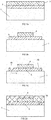
Figures 1a to 1g illustrate the process of transfer printing a III-V coupon onto an SOI substrate, in accordance with the prior art. -
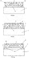
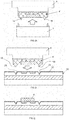
Figures 2a to 2j illustrate a process for transfer-printing a III-V coupon in accordance with a preferred embodiment of the invention. - The process steps for the transfer printing of an array of III-V coupons according to presently known technology is first described. The process is however applicable to an array as well as to a single coupon. Details of the process may be found in the above-cited publication by De Groote et al. As shown in
Figure 1a , a III-V source substrate 1 is provided and a number of layers are produced on the substrate. The first is arelease layer 2, followed by afunctional layer 3, which is usually a multilayer comprising one or more layers which are to serve as constituent layers of the eventual semiconductor component that is to be produced, for example a stack of III-V layers designed for forming an opto-electronic component such as a light-emitting diode. Thefunctional layer 3 may further comprise one or more sacrificial layers on top of the constituent component layers for increasing the mechanical strength of the coupons which are to be transferred. Thesecoupons 4 are subsequently patterned as portions of thefunctional layer 3 using lithography and etching, as illustrated inFigure 1b . Therelease layer 2 is equally patterned, thereby creating an array ofseparate islands 5 of the release layer, with III-Vcoupons 4 on the islands. The array is then covered (Figure 1c ) by aconformal encapsulation layer 6, for example a polymer photoresist. Theencapsulation layer 6 is then patterned so that it remains on top of the III-Vcoupons 4 and in selected areas around the coupons, theareas forming tethers 7 which anchor thecoupons 4 to thesource substrate 1. Therelease layer islands 5 are then removed,Figure 1d , for example by a wet etchant, thereby undercutting thecoupons 4 and leaving thecoupons 4 attached only by thetethers 7, ready for transfer printing. As illustrated inFigure 1e , the coupons are picked up by astamp 8 which is laminated against the coupon array. - The
stamp 8 may comprise a sheet of an flexible material, preferably an elastomeric material such as PDMS, pressed against the full array of coupons, in order to pick up all the coupons of the full array simultaneously, or it may be a patterned stamp, which is formed as a base provided with posts of the flexible material, wherein the posts are positioned to pick up selected coupons of the array. The latter approach allows a so-called area magnification described in more detail in the cited article by De Groote et al, i.e. a process wherein the pitch of the coupons on the source substrate can be much denser than the pitch on the target substrate. When thestamp 8 is retracted, thetethers 7 are broken and thecoupon 4 is transferred to a target substrate 10 (Figure 1f ), which may be a silicon-on-insulator (SOI) substrate comprising aphotonic waveguide circuit 11 to which the III-V coupon 4 is to be coupled. Anadhesive layer 12, for example a divinylsiloxane-bis-benzocyclobutene (DVS-BCB) layer may be spin-coated on the SOI substrate for establishing an adhesive bond between thecoupon 4 and thetarget substrate 10. After removing the encapsulation layer 6 (Figure 1g ), thecoupon 4 may then be further processed, for example by removal of the sacrificial strengthening layers and by additional patterning, to form the final III-V opto-electronic device coupled to the SOI. - In the above-described process as it is known today, the alignment of the
coupons 4 to thetarget substrate 10 is usually realised through visual alignment markers included on the coupons and on the target substrate, and by alignment software. As stated, the accuracy of such alignment techniques is often insufficient, in particular when large arrays of coupons are transferred. In this case, the visual alignment markers may be aligned for one coupon or for part of the coupons, but errors in the pitch of the array often make it impossible to achieve accurate alignment over the complete area of the array. The planar dimensions of III-V coupons are in the order of micrometres and may be anything between 10 micrometers and a few hundred micrometres. As stated, the currently obtainable minimum alignment error when large arrays of III-V coupons of this size are transfer printed is in the order of 1.5µm (3σ). - The method of the invention is an improvement in terms of the alignment quality, and allows to improve the alignment accuracy to for example about 0.5µm 3σ. The process steps according to a preferred embodiment of a method of the invention are illustrated in
Figures 2a to 2j , for an example wherein an array of III-V coupons is coupled to an SOI target substrate, although the method is applicable to any type of coupon and target substrate, and to an array as well as to a single coupon.Figures 2a and 2b show the same steps as in the already described prior art process: deposition and patterning of arelease layer 2 and afunctional layer 3 on a III-V source substrate 1, to form on thesubstrate 1 an array ofislands 5 of the release layer material and the III-V coupons 4. In an additional lithography and etch step illustrated inFigure 2c ,hollow alignment markers 15 are formed in each of therelease layer islands 5. In eachisland 5, thehollow alignment markers 15 are produced in one or more areas of the island that extend outward laterally from the circumference of thecoupon 4, i.e. the hollow alignment markers are formed in one or more areas of the island that are lateral to the area where thecoupon 4 is located. - The
hollow alignment markers 15 are cavities which are open to the exposed surface (the surface facing away from the source substrate 1) of therelease layer islands 5 and which have one or more slanted sidewalls, slanting downward from the exposed surface of therelease layer island 5 towards the bottom of the cavity. For example, grooves or holes having a V-shaped cross-section may be produced, as shown in the drawings. One known way of producing such grooves or for forming holes having the shape of an inverted pyramid is to apply an anisotropic etch process wherein the openings etched in the surface progress according to predefined angles defined by the crystallographic planes of the material. This technique is applicable for producing thehollow alignment markers 15 provided that the release layer material is a crystalline material and that the crystallographic structure of the release layer material is suitable for applying the technique. The invention is however not limited to a particular technique for producing thehollow alignment markers 15. Any known technique which forms for example conical holes or grooves with a trapezium-shaped cross section are equally suitable. The hollow alignment markers do not need to have straight slanting walls, nor do they need to be symmetrically shaped relative to a centre plane, like the V-grooves. It is important that the sidewalls are slanted downward towards each other, i.e. the angle α (seeFig. 2c ) between the surface of theisland 5 and the sidewalls at their intersection with the surface is an obtuse (blunt) angle. This requirement is related to the fact that thehollow alignment markers 15 will serve further in the process as moulds for the formation of solid alignment markers (see further) which need to engage in a lock-and-key manner with additional, complementary hollow alignment markers in the target substrate. - The lithography and etch process for defining the array of
islands 5 andcoupons 4 is designed such that eachisland 5 extends laterally outward from the circumference of the associated coupon to a sufficient degree to allow the production of thealignment markers 15, taking into account the required dimensions of the hollow alignment markers. In the case of transfer printing of III-V coupons in the above-indicated size range of 10 micrometers to a few hundred micrometres, the transverse dimension of the hollow alignment markers as seen in the plane of therelease layer 2, for example the width of thehollow alignment markers 15 in the plane, is in the order of micrometres, for example between 1 and 10/µm. Theisland 5 extends outward laterally from the associatedcoupon 4 at least at one side of the coupon, preferably at least at two opposite sides. The most preferred case is the one shown in the drawings, wherein thecoupons 4 are centrally placed on theislands 5, leaving an area surrounding the coupons, in which thehollow alignment markers 15 may be produced. In eachisland 5, at least onehollow alignment marker 15 is produced. Preferably a plurality of hollow alignment markers is formed in each island, for example a pair of V-shaped grooves, symmetrically placed at two opposing sides of thecoupon 4, as illustrated in the drawings. - On top of the array of
islands 5 andcoupons 4, with thehollow alignment markers 15 produced in theislands 5, asupport layer 16 is deposited (Figure 2d ). This may for example be an amorphous silicon layer deposited by chemical vapour deposition, i.e. deposited by a method as known in the art. The layer fills thehollow alignment markers 15 and covers thecoupons 4. Thesupport layer 16 is then patterned (Figure 2e ) so that an array ofseparate packages 17 is formed on thesource substrate 1, each package comprising anisland 5 of the release layer, with acoupon 4 on the island, wherein thecoupon 4 is embedded in aportion 18 of the support layer material. Following this (Figure 2f ), thepackages 17 are encapsulated, as in prior art processes, by anencapsulation layer 6, preferably a polymer resist layer, which is subsequently patterned to formtethers 7 by which thepackages 17 are anchored to thesubstrate 1. Therelease layer islands 5 are removed (Figure 2g ) preferably by wet etching as in prior art methods, leaving enlarged coupons 4' attached only by thetethers 7 to thesubstrate 1. Each enlarged coupon 4' consists of an original (initial)coupon 4 embedded in theportion 18 of thesupport layer 16. As seen inFigure 2h , the enlarged coupon 4' is then picked up by astamp 8 formed of a flexible material. Thepackage 17 is shown in the drawings as having a flat upper surface following from the flat upper surface of thesupport layer 16 after its deposition. This does however not suggest that a planarization of this layer is required in a method of the invention. The flatness of the upper surface of thepackage 17 is not a requirement as such, given that thestamp 8 used in transfer printing has a degree of flexibility and thus compressibility as it is preferably formed of an elastomeric material. When the stamp picks up the package, thetethers 7 are broken according to the known transfer printing practice. The removal of the release layer material results in the appearance ofsolid alignment markers 19 on the underside of the enlarged coupon 4'. Thesolid alignment markers 19 are formed from the material of thesupport layer 16 that has filled thehollow alignment markers 15 produced in the release layer islands, i.e. the size and shape of thesolid alignment markers 19 is essentially the negative of the size and shape of thehollow alignment markers 15, i.e. thesolid alignment markers 19 and thehollow alignment markers 15 have a complementary shape of essentially the same size. - As seen in
Figure 2i ,hollow alignment markers 25 are formed at the surface of thetarget substrate 10, which may for example be an SOI substrate provided with aphotonic circuit 11 and anadhesive layer 12. The size and shape of thehollow alignment markers 25 corresponds to the size and shape of thesolid alignment markers 19 in the sense that thesolid alignment markers 19 may engage with thehollow alignment markers 25 such that when the solid and hollow alignment markers are fully engaged in a lock-and-key manner, the underside of thecoupon 4 comes into contact with thetarget substrate 10. To this aim, thehollow alignment markers 25 produced in the target substrate are preferably slightly larger than thehollow alignment markers 15 originally produced in therelease layer 2. The exact size difference is controllable through the control of the respective processes (e.g. lithography, anisotropic etching) applied for producing thehollow alignment markers adhesion layer 12 depends on the type of adhesion material that is applied. In a number of cases, the thickness is negligible compared to the dimensions of the alignment markers. If this is not the case, the thickness and possibly the compressibility of theadhesion layer 12 needs to be taken into account in the dimensioning of thehollow alignment markers - The enlarged coupon 4' is aligned to the
target substrate 10 and placed onto the substrate by thestamp 8. An initial alignment, i.e. before engagement of the alignment markers, may take place according to any known method, such as the inclusion of visual alignment markers and alignment software. At this point, the outer end of the solid alignment markers 19 (e.g. the tip or ridge in the case of V-shaped holes or grooves) is positioned within the footprint of the correspondinghollow alignment markers 25. The enlarged coupon 4' is then placed onto the target substrate such that it comes into physical contact with theadhesion layer 12. Thesolid alignment markers 19 on the enlarged coupon 4' engage with thehollow alignment markers 25 in thetarget substrate 10, thereby obtaining a final alignment. The final alignment is established by the engagement of thesolid alignment markers 19 with thehollow alignment markers 25, the engagement guiding and forcing the enlarged coupon 4' into a predetermined position defined by the respective alignment markers, resulting in a self-aligning effect (final alignment). Any misalignment remaining after the initial alignment between thealignment markers original coupon 4 becomes attached to the target substrate. The angle of the slanted sidewalls of thesolid alignment markers 19 and thehollow alignment markers 25 is chosen so as to ensure that the tip or ridge of thesolid alignment markers 19 may be placed within the footprint of thehollow alignment markers 25 by the initial alignment, and so as to enable the full engagement by sliding of thesolid alignment markers 19 into the fully engaged position. - The operation of the
stamp 8 is preferably as described in the article by De Groote et al, in that the speed of the stamp is higher when the stamp is retracted from the source substrate than from the target substrate. The high retraction speed from the source substrate results in the breaking of thetethers 7, while a lower retraction speed after transfer printing to the target substrate releases the stamp from theencapsulation layer 6. Theencapsulation layer 6 and theportions 18 of the support layer are then stripped, leaving the original III-V coupon 4 coupled to the target substrate (Figure 2j ). The alignment accuracy depends on the accuracy of the lithography and etch processes used for forming thehollow alignment markers hollow alignment markers 15 with respect to thecoupon 4 and the relative position of thehollow alignment markers 25 with respect to the target location on the target substrate where the coupon is to be placed. The accuracy of these processes is high and thus allows the accuracy of the alignment in the transfer processing to be improved over existing methods, regardless of the number of coupons that is transferred. The fact that thesolid alignment markers 19 are applied to alayer 16/18 in which the original III-V coupon 4 is embedded results in an improved alignment without requiring dedicated processing of the III-V coupons 4 themselves. - When a large array of coupons is transfer printed by the method of the invention, the initial alignment of the complete array prior to the actual placement of the coupons may be done by visual markers as explained above or by any other known alignment method. As the array of coupons is subsequently placed on the target substrate, any errors caused by pitch deviations in the array may be compensated through the 3-dimensional alignment markers applied in the method of the invention. In other words, as the array of coupons approaches the target substrate, individual coupons may be shifted into place, relative to other coupons of the array, under the influence of the engaging alignment markers, thereby achieving the same alignment accuracy of the individual coupons across the complete array. The relative shift of one coupon to another is enabled by the flexibility of the stamp material. The method of the invention thus provides a considerable improvement when applied to the transfer printing of large arrays of coupons. The method is however also applicable to small arrays as well as to individual coupons.
- The method is also applicable to the transfer of a limited number of coupons from a large array by a patterned stamp which makes contact to the source and target substrate only in selected positions. This is the so-called area magnification referred to above. The same advantage is achieved here in terms of the obtainable alignment accuracy as in the case of the transfer of a complete array of coupons. Whether a stamp is used that picks up all the coupons at the same time, or a patterned stamp provided with posts for picking up selected coupons, the flexibility of the stamp material allows for a relative shift of the coupons to thereby enable the mutual engaging of the solid and
hollow alignment markers - The method of the invention is not limited to the above-described embodiments nor to the materials cited. Other materials may be chosen for the
support layer 16 for example, such as silicon nitride or silicon oxide. The material of the support layer is selected to be able to fill thehollow alignment markers 15 when deposited and subsequently form a layer having sufficient hardness to formsolid alignment markers 19 having suitable mechanical properties for the purpose of establishing the alignment by the lock-and-key engagement of thesolid alignment markers 19 with thehollow alignment markers 25 in the target substrate. The material of thesupport layer 16 is preferably selected to have a good etching selectivity relative to the material of the target substrate, more in particular the material of an upper layer of the target substrate, this to enable selective removal of thesupport layer portions 18 from the target substrate after the transfer printing. - A further advantage of the method of the invention is that it allows a greater flexibility of the production process of the semiconductor components which are to be coupled to the target substrate. In the production of III-V opto-electronic components, crucial production steps have in the past often been executed after the transfer of III-V coupons to the target substrate, precisely because of the lower alignment accuracy that could be achieved. Process steps for which the alignment requirements are most critical had to be done after the transfer. Processing on the target substrate is however in many cases technically challenging or costly. The present method allows the performance of all or of an increased number of process steps on the source wafer. It is therefore an advantage of a method of the invention that devices can be tested on the source wafer, i.e. before their transfer to the target substrate. This allows to select only good working devices for the actual transfer.
- Any details of the process described in the article by De Groote et al cited above and not related to the
support layer 16/18 or the 3-dimensional alignment markers - The invention is related also to a device assembly produced by a method of the invention, comprising at least one semiconductor component coupled to a target substrate, which may be a portion of the original target substrate obtained by sawing or other methods of sectioning the target substrate. Such a device assembly is characterized by the presence of the
hollow alignment markers 25 in the target substrate portion in an area adjacent to and/or surrounding the at least one semiconductor component coupled to the target substrate portion. The hollow alignment markers are typically filled in the finished device assembly, by additional layers deposited during the further processing or packaging of the device assembly. However, when thesealignment markers 25 are observable in the device assembly, it is clear from the fact that the alignment markers are present adjacent to the at least one coupled semiconductor component, that the method of the invention was applied in the production process of the device assembly. - While the invention has been illustrated and described in detail in the drawings and foregoing description, such illustration and description are to be considered illustrative or exemplary and not restrictive. Other variations to the disclosed embodiments can be understood and effected by those skilled in the art in practicing the claimed invention, from a study of the drawings, the disclosure and the appended claims. In the claims, the word "comprising" does not exclude other elements or steps, and the indefinite article "a" or "an" does not exclude a plurality. The mere fact that certain measures are recited in mutually different dependent claims does not indicate that a combination of these measures cannot be used to advantage. Any reference signs in the claims should not be construed as limiting the scope.
Claims (10)
- A method for coupling at least one semiconductor component to a target substrate, the method comprising the steps of:- providing on a surface of a source substrate (1) a release layer (2);- providing on the release layer (2) a functional layer (3), the functional layer consisting of or comprising one or more constituent layers of the at least one semiconductor component;- patterning the release layer (2) and the functional layer (3) to form on the surface of the source substrate (1) at least one island (5) from the release layer with a coupon (4) formed from the functional layer on the at least one island, the at least one island (5) extending outward laterally from at least one side of a circumference of the coupon (4) formed thereon, wherein the coupon consists of or comprises the at least one semiconductor component or at least one intermediate component that is to be further processed for producing the at least one semiconductor component;- forming one or more hollow alignment markers (15) at an exposed surface of the at least one island (5) in one or more areas extending outward from the coupon (4) formed thereon;- forming a support layer (16) covering the at least one island (5) and the coupon (4) formed thereon, thereby filling the hollow alignment markers (15) and embedding the at least one island (5) and the coupon (4) formed thereon in the support layer (16);- patterning the support layer (16), thereby forming at least one package (17) on the source substrate, the at least one package comprising the at least one island (5) and the coupon (4) formed thereon, embedded in a portion (18) of the support layer;- forming an encapsulating layer (6) on the at least one package (17) and patterning the encapsulating layer, thereby covering an upper surface of the at least one package (17) with the patterned encapsulating layer and forming tethers (7) of the encapsulating layer material, anchoring the at least one package to the source substrate (1);- removing the at least one island (5), thereby forming at least one enlarged coupon (4') attached only by the tethers (7) to the source substrate (1), the at least one enlarged coupon (4') consisting of the portion (18) of the support layer with the coupon (4) embedded therein, the at least one enlarged coupon (4') comprising solid alignment markers (19) formed on an underside thereof, the solid alignment markers being formed from the material of the support layer (16) that has previously filled the hollow alignment markers (15) in the release layer (2);- picking up the at least one enlarged coupon (4') by a stamp (8) suitable for transfer printing, the stamp being produced from a flexible material;- forming at a surface of a target substrate (10) hollow alignment markers (25) corresponding to the solid alignment markers (19) formed on the underside of the at least one enlarged coupon (4'), enabling engagement of the solid alignment markers (19) with the hollow alignment markers (25) of the target substrate;- performing an initial alignment, thereby aligning the at least one enlarged coupon (4') to a predetermined location on the target substrate (10);- placing the at least one enlarged coupon (4') onto the target substrate, thereby establishing a final alignment by engagement of the solid alignment markers (19) of the at least one enlarged coupon (4') with the hollow alignment markers (25) of the target substrate (10), up to the point where the coupon (4) of the at least one enlarged coupon (4') becomes attached to the surface of the target substrate (10), thereby aligning and attaching at least one coupon (4) to the target substrate; and- releasing the stamp (8) and removing the encapsulation layer (6) and the portion (18) of the support layer, thereby leaving the at least one coupon (4) attached to the target substrate (10),thereby obtaining the at least one semiconductor component coupled to the target substrate, or performing further processing steps on the at least one coupon (4) for producing the at least one semiconductor component.
- The method according to claim 1, wherein an array of coupons (4) is formed on the source substrate (1) and wherein all coupons of the array are simultaneously transferred to the target substrate (10).
- The method according to claim 1, wherein an array of coupons (4) is formed on the source substrate (1) and wherein selected coupons of the array are simultaneously transferred to the target substrate (10).
- The method according to any one of the previous claims, wherein the at least one semiconductor component is a III-V optoelectronic component and wherein the target substrate (10) comprises an optical circuit (11) to which the optoelectronic component is to be coupled.
- The method according to any one of the previous claims, wherein each of the hollow alignment markers (15, 25) produced in the islands (5) of release layer material and in the target substrate (10) has slanted side walls oriented downward from the surface respectively of the islands (5) and of the target substrate (10) and slanted towards each other.
- The method according to claim 5, wherein the hollow alignment markers (15, 25) are V-shaped grooves or holes.
- The method according to any one of previous claims, wherein the material of the support layer (16) is chosen from the group of amorphous silicon, silicon nitride and silicon oxide.
- A semiconductor device assembly comprising a target substrate portion and at least one semiconductor component coupled thereto, wherein the target substrate portion comprises one or more hollow alignment markers (25) located adjacent to the at least one semiconductor component.
- The semiconductor device according to claim 8, wherein each of the hollow alignment markers (25) has slanted side walls oriented downward from the surface of the target substrate portion and slanted towards each other.
- The semiconductor device according to claim 9, wherein the hollow alignment markers (25) are V-shaped grooves or holes.
Priority Applications (3)
| Application Number | Priority Date | Filing Date | Title |
|---|---|---|---|
| EP18165502.8A EP3550603B1 (en) | 2018-04-03 | 2018-04-03 | A method for coupling a semiconductor component to a target substrate by transfer printing |
| CN201910241596.7A CN110349912B (en) | 2018-04-03 | 2019-03-28 | Method for coupling a semiconductor component to a target substrate by transfer printing |
| US16/371,754 US10847673B2 (en) | 2018-04-03 | 2019-04-01 | Coupling a semiconductor component to a target substrate by transfer printing |
Applications Claiming Priority (1)
| Application Number | Priority Date | Filing Date | Title |
|---|---|---|---|
| EP18165502.8A EP3550603B1 (en) | 2018-04-03 | 2018-04-03 | A method for coupling a semiconductor component to a target substrate by transfer printing |
Publications (2)
| Publication Number | Publication Date |
|---|---|
| EP3550603A1 true EP3550603A1 (en) | 2019-10-09 |
| EP3550603B1 EP3550603B1 (en) | 2020-11-18 |
Family
ID=61906637
Family Applications (1)
| Application Number | Title | Priority Date | Filing Date |
|---|---|---|---|
| EP18165502.8A Active EP3550603B1 (en) | 2018-04-03 | 2018-04-03 | A method for coupling a semiconductor component to a target substrate by transfer printing |
Country Status (3)
| Country | Link |
|---|---|
| US (1) | US10847673B2 (en) |
| EP (1) | EP3550603B1 (en) |
| CN (1) | CN110349912B (en) |
Families Citing this family (7)
| Publication number | Priority date | Publication date | Assignee | Title |
|---|---|---|---|---|
| CN111244227B (en) * | 2020-01-19 | 2023-07-18 | 中国科学院上海微系统与信息技术研究所 | A silicon-based photonic integrated module and its preparation method |
| GB2593260B (en) * | 2020-03-17 | 2024-06-26 | Rockley Photonics Ltd | Coupon wafer and method of preparation thereof |
| GB2595948B (en) * | 2020-10-26 | 2022-12-07 | Rockley Photonics Ltd | Coupon wafer and method of preparation thereof |
| CN114068372B (en) * | 2020-07-29 | 2025-10-17 | 华为技术有限公司 | Transfer assembly and transfer method for Micro LED crystal grains |
| CN112606585B (en) * | 2020-12-02 | 2022-05-31 | 潍坊歌尔微电子有限公司 | Device transfer processing method and transfer processing method of micro-microphone dustproof device |
| EP4578040A1 (en) * | 2022-08-22 | 2025-07-02 | Universiteit Gent | Micro-transfer printing of thin films |
| NL2037448B1 (en) | 2024-04-12 | 2025-11-03 | Univ Eindhoven Tech | Photonic-integrated SOA for varying mode profile to combine high gain and high power |
Citations (4)
| Publication number | Priority date | Publication date | Assignee | Title |
|---|---|---|---|---|
| US20040142575A1 (en) * | 2002-07-25 | 2004-07-22 | Brewer Peter D. | Large area printing method for integrating device and circuit components |
| US20130181339A1 (en) * | 2012-01-12 | 2013-07-18 | Mars Technology | Multi-chip self-alignment assembly which can be used with flip-chip bonding |
| US20170170127A1 (en) * | 2015-12-11 | 2017-06-15 | SK Hynix Inc. | Semiconductors, packages, wafer level packages, and methods of manufacturing the same |
| WO2017169485A1 (en) * | 2016-03-30 | 2017-10-05 | パナソニックIpマネジメント株式会社 | Semiconductor device |
Family Cites Families (16)
| Publication number | Priority date | Publication date | Assignee | Title |
|---|---|---|---|---|
| US5492223A (en) * | 1994-02-04 | 1996-02-20 | Motorola, Inc. | Interlocking and invertible semiconductor device tray and test contactor mating thereto |
| US5888884A (en) * | 1998-01-02 | 1999-03-30 | General Electric Company | Electronic device pad relocation, precision placement, and packaging in arrays |
| JP2008507114A (en) | 2004-04-27 | 2008-03-06 | ザ ボード オブ トラスティーズ オブ ザ ユニヴァーシティー オブ イリノイ | Composite patterning device for soft lithography |
| JP5049787B2 (en) * | 2004-11-04 | 2012-10-17 | マイクロチップス・インコーポレーテッド | Cold pressure sealing method and apparatus |
| US7373052B2 (en) * | 2006-05-05 | 2008-05-13 | Sioptical, Inc. | Passive fiber alignment arrangement for coupling to nano-taper optical waveguides |
| DE102009060277A1 (en) * | 2008-12-24 | 2010-09-02 | X-Fab Semiconductor Foundries Ag | Method for producing alignment marks for light-impermeable or light-absorbing layers (light shield resist masks) |
| US8247895B2 (en) * | 2010-01-08 | 2012-08-21 | International Business Machines Corporation | 4D device process and structure |
| US8373259B2 (en) * | 2010-07-27 | 2013-02-12 | Intel Corporation | Optical connection through single assembly overhang flip chip optics die with micro structure alignment |
| WO2013112208A2 (en) | 2011-10-06 | 2013-08-01 | Massachusetts Institute Of Technology | Compactly-integrated optical detectors and associated systems and methods |
| CN103094182B (en) * | 2011-10-28 | 2015-06-17 | 中芯国际集成电路制造(北京)有限公司 | Manufacturing method for semiconductor device |
| TWI546979B (en) * | 2012-03-05 | 2016-08-21 | 晶元光電股份有限公司 | Parallel bonded light emitting diode device and manufacturing method thereof |
| US9875974B2 (en) | 2013-03-08 | 2018-01-23 | The Board Of Trustees Of The University Of Illinois | Processing techniques for silicon-based transient devices |
| US9385222B2 (en) * | 2014-02-14 | 2016-07-05 | Infineon Technologies Ag | Semiconductor device with insert structure at a rear side and method of manufacturing |
| US20160023904A1 (en) * | 2014-07-28 | 2016-01-28 | Massachusetts Institute Of Technology | Strain engineered microstructures |
| US9576595B1 (en) | 2014-11-19 | 2017-02-21 | Seagate Technology Llc | Transfer printing an epitaxial layer to a read/write head to form an integral laser |
| US20190378781A1 (en) * | 2018-06-07 | 2019-12-12 | International Business Machines Corporation | Enhanced adhesive materials and processes for 3d applications |
-
2018
- 2018-04-03 EP EP18165502.8A patent/EP3550603B1/en active Active
-
2019
- 2019-03-28 CN CN201910241596.7A patent/CN110349912B/en active Active
- 2019-04-01 US US16/371,754 patent/US10847673B2/en active Active
Patent Citations (5)
| Publication number | Priority date | Publication date | Assignee | Title |
|---|---|---|---|---|
| US20040142575A1 (en) * | 2002-07-25 | 2004-07-22 | Brewer Peter D. | Large area printing method for integrating device and circuit components |
| US20130181339A1 (en) * | 2012-01-12 | 2013-07-18 | Mars Technology | Multi-chip self-alignment assembly which can be used with flip-chip bonding |
| US20170170127A1 (en) * | 2015-12-11 | 2017-06-15 | SK Hynix Inc. | Semiconductors, packages, wafer level packages, and methods of manufacturing the same |
| WO2017169485A1 (en) * | 2016-03-30 | 2017-10-05 | パナソニックIpマネジメント株式会社 | Semiconductor device |
| US20180197802A1 (en) * | 2016-03-30 | 2018-07-12 | Panasonic Intellectual Property Management Co., Ltd. | Semiconductor device |
Non-Patent Citations (2)
| Title |
|---|
| ANDREAS DE GROOTE ET AL: "Transfer-printing-based integration ofsingle-mode waveguide-coupledIII-V-on-silicon broadband light emitters", OPTICS EXPRESS,, vol. 24, no. 13, 27 June 2016 (2016-06-27), pages 13754 - 13762, XP002770905, DOI: 10.1364/OE.24.013754 * |
| DE GROOTE ET AL.: "Transfer-printing-based integration of single-mode waveguide-coupled III-V-on-silicon broadband light emitters", OPTICAL SOCIETY OF AMERICA, 13 June 2016 (2016-06-13) |
Also Published As
| Publication number | Publication date |
|---|---|
| EP3550603B1 (en) | 2020-11-18 |
| US10847673B2 (en) | 2020-11-24 |
| CN110349912B (en) | 2024-03-29 |
| US20190305179A1 (en) | 2019-10-03 |
| CN110349912A (en) | 2019-10-18 |
Similar Documents
| Publication | Publication Date | Title |
|---|---|---|
| EP3550603B1 (en) | A method for coupling a semiconductor component to a target substrate by transfer printing | |
| US8847079B2 (en) | Method for producing an integrated device | |
| US8258011B2 (en) | Method for producing a set of chips mechanically interconnected by means of a flexible connection | |
| EP3295492B1 (en) | Printable inorganic semiconductor structures | |
| US20210074573A1 (en) | Integration of microdevices into system substrate | |
| US6392144B1 (en) | Micromechanical die attachment surcharge | |
| US9006896B2 (en) | Chip package and method for forming the same | |
| EP3555912B1 (en) | Isolation structure for micro-transfer-printable devices | |
| CN110634783B (en) | Apparatus and method for transferring chips from source substrate to target substrate | |
| KR20190076690A (en) | Transfer Method using Deformable Film | |
| TW202121572A (en) | High-precision printed structures | |
| US12374675B2 (en) | Method of producing hybrid semiconductor wafer | |
| KR101939013B1 (en) | Method and apparatus for separating a microchip from a wafer and placing the microchip on the substrate | |
| KR20150046253A (en) | Micro device stabilization post | |
| US8405210B2 (en) | Method for producing a plurality of chips and a chip produced accordingly | |
| US20080050561A1 (en) | Micromechanical Component With Active Elements and Method Producing a Component of This Type | |
| KR102656505B1 (en) | Die-to-wafer bonding utilizing micro-transfer printing | |
| JP2018501636A (en) | Transfer printing method | |
| EP3929641A1 (en) | A semiconductor package comprising one or more optical integrated circuits | |
| US20030030455A1 (en) | Test probe having a sheet body | |
| TW202335242A (en) | Method for transferring an optoelectronic device | |
| KR20230009368A (en) | Method and system for transferring alignment marks between substrate systems | |
| KR100806380B1 (en) | Probe card manufacturing method and probe card thereby | |
| US11037812B2 (en) | Method for a transfer print between substrates | |
| TWI922065B (en) | Semiconductor stacked body and manufacturing method of semiconductor device |
Legal Events
| Date | Code | Title | Description |
|---|---|---|---|
| PUAI | Public reference made under article 153(3) epc to a published international application that has entered the european phase |
Free format text: ORIGINAL CODE: 0009012 |
|
| STAA | Information on the status of an ep patent application or granted ep patent |
Free format text: STATUS: THE APPLICATION HAS BEEN PUBLISHED |
|
| AK | Designated contracting states |
Kind code of ref document: A1 Designated state(s): AL AT BE BG CH CY CZ DE DK EE ES FI FR GB GR HR HU IE IS IT LI LT LU LV MC MK MT NL NO PL PT RO RS SE SI SK SM TR |
|
| AX | Request for extension of the european patent |
Extension state: BA ME |
|
| STAA | Information on the status of an ep patent application or granted ep patent |
Free format text: STATUS: REQUEST FOR EXAMINATION WAS MADE |
|
| 17P | Request for examination filed |
Effective date: 20200316 |
|
| RBV | Designated contracting states (corrected) |
Designated state(s): AL AT BE BG CH CY CZ DE DK EE ES FI FR GB GR HR HU IE IS IT LI LT LU LV MC MK MT NL NO PL PT RO RS SE SI SK SM TR |
|
| GRAP | Despatch of communication of intention to grant a patent |
Free format text: ORIGINAL CODE: EPIDOSNIGR1 |
|
| STAA | Information on the status of an ep patent application or granted ep patent |
Free format text: STATUS: GRANT OF PATENT IS INTENDED |
|
| GRAS | Grant fee paid |
Free format text: ORIGINAL CODE: EPIDOSNIGR3 |
|
| INTG | Intention to grant announced |
Effective date: 20200918 |
|
| GRAA | (expected) grant |
Free format text: ORIGINAL CODE: 0009210 |
|
| STAA | Information on the status of an ep patent application or granted ep patent |
Free format text: STATUS: THE PATENT HAS BEEN GRANTED |
|
| AK | Designated contracting states |
Kind code of ref document: B1 Designated state(s): AL AT BE BG CH CY CZ DE DK EE ES FI FR GB GR HR HU IE IS IT LI LT LU LV MC MK MT NL NO PL PT RO RS SE SI SK SM TR |
|
| REG | Reference to a national code |
Ref country code: GB Ref legal event code: FG4D |
|
| REG | Reference to a national code |
Ref country code: CH Ref legal event code: EP |
|
| REG | Reference to a national code |
Ref country code: IE Ref legal event code: FG4D |
|
| REG | Reference to a national code |
Ref country code: DE Ref legal event code: R096 Ref document number: 602018009737 Country of ref document: DE |
|
| REG | Reference to a national code |
Ref country code: AT Ref legal event code: REF Ref document number: 1336702 Country of ref document: AT Kind code of ref document: T Effective date: 20201215 |
|
| REG | Reference to a national code |
Ref country code: AT Ref legal event code: MK05 Ref document number: 1336702 Country of ref document: AT Kind code of ref document: T Effective date: 20201118 |
|
| REG | Reference to a national code |
Ref country code: NL Ref legal event code: MP Effective date: 20201118 |
|
| PG25 | Lapsed in a contracting state [announced via postgrant information from national office to epo] |
Ref country code: GR Free format text: LAPSE BECAUSE OF FAILURE TO SUBMIT A TRANSLATION OF THE DESCRIPTION OR TO PAY THE FEE WITHIN THE PRESCRIBED TIME-LIMIT Effective date: 20210219 Ref country code: NO Free format text: LAPSE BECAUSE OF FAILURE TO SUBMIT A TRANSLATION OF THE DESCRIPTION OR TO PAY THE FEE WITHIN THE PRESCRIBED TIME-LIMIT Effective date: 20210218 Ref country code: FI Free format text: LAPSE BECAUSE OF FAILURE TO SUBMIT A TRANSLATION OF THE DESCRIPTION OR TO PAY THE FEE WITHIN THE PRESCRIBED TIME-LIMIT Effective date: 20201118 Ref country code: RS Free format text: LAPSE BECAUSE OF FAILURE TO SUBMIT A TRANSLATION OF THE DESCRIPTION OR TO PAY THE FEE WITHIN THE PRESCRIBED TIME-LIMIT Effective date: 20201118 Ref country code: PT Free format text: LAPSE BECAUSE OF FAILURE TO SUBMIT A TRANSLATION OF THE DESCRIPTION OR TO PAY THE FEE WITHIN THE PRESCRIBED TIME-LIMIT Effective date: 20210318 |
|
| PG25 | Lapsed in a contracting state [announced via postgrant information from national office to epo] |
Ref country code: AT Free format text: LAPSE BECAUSE OF FAILURE TO SUBMIT A TRANSLATION OF THE DESCRIPTION OR TO PAY THE FEE WITHIN THE PRESCRIBED TIME-LIMIT Effective date: 20201118 Ref country code: SE Free format text: LAPSE BECAUSE OF FAILURE TO SUBMIT A TRANSLATION OF THE DESCRIPTION OR TO PAY THE FEE WITHIN THE PRESCRIBED TIME-LIMIT Effective date: 20201118 Ref country code: IS Free format text: LAPSE BECAUSE OF FAILURE TO SUBMIT A TRANSLATION OF THE DESCRIPTION OR TO PAY THE FEE WITHIN THE PRESCRIBED TIME-LIMIT Effective date: 20210318 Ref country code: PL Free format text: LAPSE BECAUSE OF FAILURE TO SUBMIT A TRANSLATION OF THE DESCRIPTION OR TO PAY THE FEE WITHIN THE PRESCRIBED TIME-LIMIT Effective date: 20201118 Ref country code: LV Free format text: LAPSE BECAUSE OF FAILURE TO SUBMIT A TRANSLATION OF THE DESCRIPTION OR TO PAY THE FEE WITHIN THE PRESCRIBED TIME-LIMIT Effective date: 20201118 Ref country code: BG Free format text: LAPSE BECAUSE OF FAILURE TO SUBMIT A TRANSLATION OF THE DESCRIPTION OR TO PAY THE FEE WITHIN THE PRESCRIBED TIME-LIMIT Effective date: 20210218 |
|
| REG | Reference to a national code |
Ref country code: LT Ref legal event code: MG9D |
|
| PG25 | Lapsed in a contracting state [announced via postgrant information from national office to epo] |
Ref country code: HR Free format text: LAPSE BECAUSE OF FAILURE TO SUBMIT A TRANSLATION OF THE DESCRIPTION OR TO PAY THE FEE WITHIN THE PRESCRIBED TIME-LIMIT Effective date: 20201118 |
|
| PG25 | Lapsed in a contracting state [announced via postgrant information from national office to epo] |
Ref country code: SM Free format text: LAPSE BECAUSE OF FAILURE TO SUBMIT A TRANSLATION OF THE DESCRIPTION OR TO PAY THE FEE WITHIN THE PRESCRIBED TIME-LIMIT Effective date: 20201118 Ref country code: EE Free format text: LAPSE BECAUSE OF FAILURE TO SUBMIT A TRANSLATION OF THE DESCRIPTION OR TO PAY THE FEE WITHIN THE PRESCRIBED TIME-LIMIT Effective date: 20201118 Ref country code: CZ Free format text: LAPSE BECAUSE OF FAILURE TO SUBMIT A TRANSLATION OF THE DESCRIPTION OR TO PAY THE FEE WITHIN THE PRESCRIBED TIME-LIMIT Effective date: 20201118 Ref country code: SK Free format text: LAPSE BECAUSE OF FAILURE TO SUBMIT A TRANSLATION OF THE DESCRIPTION OR TO PAY THE FEE WITHIN THE PRESCRIBED TIME-LIMIT Effective date: 20201118 Ref country code: RO Free format text: LAPSE BECAUSE OF FAILURE TO SUBMIT A TRANSLATION OF THE DESCRIPTION OR TO PAY THE FEE WITHIN THE PRESCRIBED TIME-LIMIT Effective date: 20201118 Ref country code: LT Free format text: LAPSE BECAUSE OF FAILURE TO SUBMIT A TRANSLATION OF THE DESCRIPTION OR TO PAY THE FEE WITHIN THE PRESCRIBED TIME-LIMIT Effective date: 20201118 |
|
| REG | Reference to a national code |
Ref country code: DE Ref legal event code: R097 Ref document number: 602018009737 Country of ref document: DE |
|
| PG25 | Lapsed in a contracting state [announced via postgrant information from national office to epo] |
Ref country code: DK Free format text: LAPSE BECAUSE OF FAILURE TO SUBMIT A TRANSLATION OF THE DESCRIPTION OR TO PAY THE FEE WITHIN THE PRESCRIBED TIME-LIMIT Effective date: 20201118 |
|
| PLBE | No opposition filed within time limit |
Free format text: ORIGINAL CODE: 0009261 |
|
| STAA | Information on the status of an ep patent application or granted ep patent |
Free format text: STATUS: NO OPPOSITION FILED WITHIN TIME LIMIT |
|
| 26N | No opposition filed |
Effective date: 20210819 |
|
| PG25 | Lapsed in a contracting state [announced via postgrant information from national office to epo] |
Ref country code: IT Free format text: LAPSE BECAUSE OF FAILURE TO SUBMIT A TRANSLATION OF THE DESCRIPTION OR TO PAY THE FEE WITHIN THE PRESCRIBED TIME-LIMIT Effective date: 20201118 Ref country code: NL Free format text: LAPSE BECAUSE OF FAILURE TO SUBMIT A TRANSLATION OF THE DESCRIPTION OR TO PAY THE FEE WITHIN THE PRESCRIBED TIME-LIMIT Effective date: 20201118 Ref country code: AL Free format text: LAPSE BECAUSE OF FAILURE TO SUBMIT A TRANSLATION OF THE DESCRIPTION OR TO PAY THE FEE WITHIN THE PRESCRIBED TIME-LIMIT Effective date: 20201118 |
|
| PG25 | Lapsed in a contracting state [announced via postgrant information from national office to epo] |
Ref country code: MC Free format text: LAPSE BECAUSE OF FAILURE TO SUBMIT A TRANSLATION OF THE DESCRIPTION OR TO PAY THE FEE WITHIN THE PRESCRIBED TIME-LIMIT Effective date: 20201118 Ref country code: SI Free format text: LAPSE BECAUSE OF FAILURE TO SUBMIT A TRANSLATION OF THE DESCRIPTION OR TO PAY THE FEE WITHIN THE PRESCRIBED TIME-LIMIT Effective date: 20201118 |
|
| PG25 | Lapsed in a contracting state [announced via postgrant information from national office to epo] |
Ref country code: LU Free format text: LAPSE BECAUSE OF NON-PAYMENT OF DUE FEES Effective date: 20210403 |
|
| PG25 | Lapsed in a contracting state [announced via postgrant information from national office to epo] |
Ref country code: ES Free format text: LAPSE BECAUSE OF FAILURE TO SUBMIT A TRANSLATION OF THE DESCRIPTION OR TO PAY THE FEE WITHIN THE PRESCRIBED TIME-LIMIT Effective date: 20201118 Ref country code: LI Free format text: LAPSE BECAUSE OF NON-PAYMENT OF DUE FEES Effective date: 20210430 Ref country code: CH Free format text: LAPSE BECAUSE OF NON-PAYMENT OF DUE FEES Effective date: 20210430 |
|
| PG25 | Lapsed in a contracting state [announced via postgrant information from national office to epo] |
Ref country code: IE Free format text: LAPSE BECAUSE OF NON-PAYMENT OF DUE FEES Effective date: 20210403 |
|
| PG25 | Lapsed in a contracting state [announced via postgrant information from national office to epo] |
Ref country code: IS Free format text: LAPSE BECAUSE OF FAILURE TO SUBMIT A TRANSLATION OF THE DESCRIPTION OR TO PAY THE FEE WITHIN THE PRESCRIBED TIME-LIMIT Effective date: 20210318 |
|
| P01 | Opt-out of the competence of the unified patent court (upc) registered |
Effective date: 20230513 |
|
| PG25 | Lapsed in a contracting state [announced via postgrant information from national office to epo] |
Ref country code: CY Free format text: LAPSE BECAUSE OF FAILURE TO SUBMIT A TRANSLATION OF THE DESCRIPTION OR TO PAY THE FEE WITHIN THE PRESCRIBED TIME-LIMIT Effective date: 20201118 |
|
| PG25 | Lapsed in a contracting state [announced via postgrant information from national office to epo] |
Ref country code: HU Free format text: LAPSE BECAUSE OF FAILURE TO SUBMIT A TRANSLATION OF THE DESCRIPTION OR TO PAY THE FEE WITHIN THE PRESCRIBED TIME-LIMIT; INVALID AB INITIO Effective date: 20180403 |
|
| PG25 | Lapsed in a contracting state [announced via postgrant information from national office to epo] |
Ref country code: MK Free format text: LAPSE BECAUSE OF FAILURE TO SUBMIT A TRANSLATION OF THE DESCRIPTION OR TO PAY THE FEE WITHIN THE PRESCRIBED TIME-LIMIT Effective date: 20201118 |
|
| PG25 | Lapsed in a contracting state [announced via postgrant information from national office to epo] |
Ref country code: MT Free format text: LAPSE BECAUSE OF FAILURE TO SUBMIT A TRANSLATION OF THE DESCRIPTION OR TO PAY THE FEE WITHIN THE PRESCRIBED TIME-LIMIT Effective date: 20201118 |
|
| PGFP | Annual fee paid to national office [announced via postgrant information from national office to epo] |
Ref country code: DE Payment date: 20250319 Year of fee payment: 8 |
|
| REG | Reference to a national code |
Ref country code: DE Ref legal event code: R079 Ref document number: 602018009737 Country of ref document: DE Free format text: PREVIOUS MAIN CLASS: H01L0023544000 Ipc: H10W0046000000 |
|
| PG25 | Lapsed in a contracting state [announced via postgrant information from national office to epo] |
Ref country code: TR Free format text: LAPSE BECAUSE OF FAILURE TO SUBMIT A TRANSLATION OF THE DESCRIPTION OR TO PAY THE FEE WITHIN THE PRESCRIBED TIME-LIMIT Effective date: 20201118 |
|
| PGFP | Annual fee paid to national office [announced via postgrant information from national office to epo] |
Ref country code: GB Payment date: 20260319 Year of fee payment: 9 |
|
| PGFP | Annual fee paid to national office [announced via postgrant information from national office to epo] |
Ref country code: BE Payment date: 20260319 Year of fee payment: 9 |
|
| PGFP | Annual fee paid to national office [announced via postgrant information from national office to epo] |
Ref country code: FR Payment date: 20260320 Year of fee payment: 9 |