EP3550430B1 - Verfahren zur verarbeitung einer konfigurationsdatei, berührungschip, vorrichtung und medium - Google Patents
Verfahren zur verarbeitung einer konfigurationsdatei, berührungschip, vorrichtung und medium Download PDFInfo
- Publication number
- EP3550430B1 EP3550430B1 EP17935049.1A EP17935049A EP3550430B1 EP 3550430 B1 EP3550430 B1 EP 3550430B1 EP 17935049 A EP17935049 A EP 17935049A EP 3550430 B1 EP3550430 B1 EP 3550430B1
- Authority
- EP
- European Patent Office
- Prior art keywords
- configuration
- control chip
- touch control
- configuration file
- variable region
- Prior art date
- Legal status (The legal status is an assumption and is not a legal conclusion. Google has not performed a legal analysis and makes no representation as to the accuracy of the status listed.)
- Active
Links
Images



Classifications
-
- G—PHYSICS
- G06—COMPUTING OR CALCULATING; COUNTING
- G06F—ELECTRIC DIGITAL DATA PROCESSING
- G06F9/00—Arrangements for program control, e.g. control units
- G06F9/06—Arrangements for program control, e.g. control units using stored programs, i.e. using an internal store of processing equipment to receive or retain programs
- G06F9/44—Arrangements for executing specific programs
- G06F9/445—Program loading or initiating
- G06F9/44505—Configuring for program initiating, e.g. using registry, configuration files
-
- G—PHYSICS
- G06—COMPUTING OR CALCULATING; COUNTING
- G06F—ELECTRIC DIGITAL DATA PROCESSING
- G06F3/00—Input arrangements for transferring data to be processed into a form capable of being handled by the computer; Output arrangements for transferring data from processing unit to output unit, e.g. interface arrangements
- G06F3/01—Input arrangements or combined input and output arrangements for interaction between user and computer
- G06F3/03—Arrangements for converting the position or the displacement of a member into a coded form
- G06F3/041—Digitisers, e.g. for touch screens or touch pads, characterised by the transducing means
- G06F3/0416—Control or interface arrangements specially adapted for digitisers
-
- G—PHYSICS
- G06—COMPUTING OR CALCULATING; COUNTING
- G06F—ELECTRIC DIGITAL DATA PROCESSING
- G06F8/00—Arrangements for software engineering
- G06F8/60—Software deployment
- G06F8/65—Updates
- G06F8/654—Updates using techniques specially adapted for alterable solid state memories, e.g. for EEPROM or flash memories
-
- G—PHYSICS
- G06—COMPUTING OR CALCULATING; COUNTING
- G06F—ELECTRIC DIGITAL DATA PROCESSING
- G06F9/00—Arrangements for program control, e.g. control units
- G06F9/06—Arrangements for program control, e.g. control units using stored programs, i.e. using an internal store of processing equipment to receive or retain programs
- G06F9/44—Arrangements for executing specific programs
- G06F9/4401—Bootstrapping
- G06F9/4418—Suspend and resume; Hibernate and awake
-
- G—PHYSICS
- G06—COMPUTING OR CALCULATING; COUNTING
- G06F—ELECTRIC DIGITAL DATA PROCESSING
- G06F9/00—Arrangements for program control, e.g. control units
- G06F9/06—Arrangements for program control, e.g. control units using stored programs, i.e. using an internal store of processing equipment to receive or retain programs
- G06F9/44—Arrangements for executing specific programs
- G06F9/445—Program loading or initiating
- G06F9/44536—Selecting among different versions
Definitions
- the present application relates to the field of touch screen technology, and in particular to a method, a processing unit, a touch control chip, a device, and a medium for processing a configuration file.
- touch control chips have been widely used in smart terminals such as mobile phones, notebook computers and tablet computers.
- a touch control chip is loaded with a configuration file for algorithm modules.
- the existing configuration file is about to be exhausted, and parameters that need to be updated or added in the configuration file are gradually increased.
- a Micro Controller Unit (MCU) or a Central Processing Unit (CPU) writes the configuration file to the touch control chip as a whole.
- MCU Micro Controller Unit
- CPU Central Processing Unit
- the MCU or CPU needs to reconfigure an entire updated configuration file to the touch control chip, thereby reducing the configuration efficiency of the touch control chip.
- CN 102915284A discloses that standardized configuration information for different types of infrared touch screens are stored in a storage unit, from which corresponding configuration information is determined for a specific type of infrared touch screen.
- INI file- Wikipedia, the free encyclopedia discloses a format of an INI file, where the basic element contained in the INI file is the property, and properties may be grouped into arbitrarily named sections.
- the present invention is set out in the appended set of claims.
- the present application provides a method, a touch control chip, a device, and a medium for processing a configuration file, thereby improving configuration efficiency of a touch control chip.
- the present application provides a method for processing a configuration file, including: obtaining a configuration file of a touch control chip; parsing the configuration file to obtain a parsed configuration file; and configuring the parsed configuration file to each algorithm module of the touch control chip; where the configuration file includes a plurality of first configuration modules which are respectively used for configuring parameters of different attributes for the touch control chip; wherein the touch control chip includes a global variable region and the global variable region is used for storing at least one second configuration module, wherein the at least one second configuration module is obtained after at least one corresponding first configuration module is updated; and the method further includes: obtaining the at least one second configuration module; and parsing the at least one second configuration module, and configuring the parsed at least one second configuration module to at least one corresponding algorithm module of the touch control chip; wherein the at least one corresponding first configuration module includes a part of the plurality of first configuration modules.
- the touch control chip includes a temporary variable region which is used for temporarily storing the configuration file and a non-configuration file of the touch control chip in different time periods, respectively; and after the parsing the configuration file to obtain the parsed configuration file, the method further includes: storing the parsed configuration file to a flash memory and deleting the configuration file in the temporary variable region.
- the method further includes: receiving a read request; and reading the parsed configuration file from the flash memory to the temporary variable region according to the read request.
- storage space of the global variable region is smaller than that of the temporary variable region, and a starting storage address of the temporary variable region is smaller than that located in the global variable region.
- the touch control chip, the device and the medium are described below, and the implementation principles and technical effects thereof are similar to those of the method related to the first aspect, and the optional modes of the first aspect, which will not be described below.
- the present application provides a touch control chip, where the touch control chip is configured to: obtain a configuration file of the touch control chip; parse the configuration file to obtain a parsed configuration file; and configure the parsed configuration file to each algorithm module of the touch control chip; where the configuration file includes a plurality of first configuration modules which are respectively configured to configure parameters of different attributes for the touch control chip; wherein the touch control chip further includes a global variable region and the global variable region is configured to store at least one second configuration module, wherein the at least one second configuration module is obtained after at least one corresponding first configuration module is updated; and the touch control chip is further configured to: obtain the at least one second configuration module; and parse the at least one second configuration module, and configure the parsed at least one second configuration module to at least one corresponding algorithm module of the touch control chip; wherein the at least one corresponding first configuration module includes a part of the plurality of first configuration modules.
- the touch control chip includes a temporary variable region which is configured to temporarily store the configuration file and a non-configuration file of the touch control chip in different time periods, respectively; and the touch control chip is further configured to: store the parsed configuration file to a flash memory and delete the configuration file in the temporary variable region.
- the touch control chip is further configured to: receive a read request; and read the parsed configuration file from the flash memory to the temporary variable region according to the read request.
- storage space of the global variable region is smaller than that of the temporary variable region, and a starting storage address of the temporary variable region is smaller than that located in the global variable region.
- the present application provides a touch device including a touch control chip described in any one of the second aspect and the optional modes of the second aspect.
- the present application provides a computer storage medium including computer instructions, when executed by a computer, causing the computer to implement a method described in any one of the first aspect, and the optional modes of the first aspect.
- the present application provides a computer program product including instructions, when executed by a computer, causing the computer to perform a method described in any one of the first aspect, and the optional modes of the first aspect.
- the present application provides a method, a touch control chip, a device, and a medium for processing a configuration file.
- the method includes: determining the configuration file of a touch control chip; and writing the configuration file to the touch control chip; where the configuration file includes a plurality of first configuration modules which are respectively used for configuring parameters of different attributes for the touch control chip. Since the configuration file includes a plurality of first configuration modules, the processing unit updates a configuration module instead of reconfiguring the touch control chip when the parameters of the configuration file need to be updated or added, thereby improving the configuration efficiency of the touch control chip.
- an MCU or CPU writes a configuration file to a touch control chip as a whole.
- the MCU or CPU needs to reconfigure the touch control chip, thereby reducing the configuration efficiency of the touch control chip.
- the present application provides a method, a processing unit, a touch control chip, a device, and a medium for processing a configuration file.
- Fig. 1 is a schematic diagram of an application scenario of a method and a device for processing a configuration file provided by an embodiment of the present application.
- the touch control chip 11 may be disposed on a mobile phone, a notebook computer, a computer, a digital broadcast terminal, a messaging device, a game console, a tablet device, a medical equipment, a fitness equipment, a personal digital assistant, a kitchen appliance, a bathroom appliance, an air conditioner, a lighting lamp or other smart terminals with a touch screen, a touch pad or a touch button.
- a processing unit 12 may be an MCU, a CPU, a graphics processing unit (GPU) or the like, where the processing unit 12 is configured to write or read the configuration file or the like, to or from the touch control chip 11.
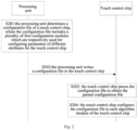
- Fig. 2 is an interaction flowchart of a method for processing a configuration file provided by an embodiment of the present application. As shown in Fig. 2 , the method includes the following process.
- Step S201 the processing unit determines a configuration file of a touch control chip, where the configuration file includes a plurality of first configuration modules which are respectively used for configuring parameters of different attributes for the touch control chip.
- the configuration file includes: a resolution and an interrupt mode of a touch screen corresponding to the touch control chip, a working frequency band of the touch control chip, a type of the touch control chip, etc.
- the type of the touch control chip includes self-capacitance and mutual capacitance.
- the configuration file includes a plurality of first configuration modules.
- Fig. 3 is a schematic diagram of a format of a configuration file provided by an embodiment of the present application.
- the configuration file includes a packet header and n+1 first configuration modules, that is, the first configuration module 1, the first configuration module 2, ..., the first configuration module n+1.
- the packet header includes a configuration version number, a configuration flag, a total packet number of the configuration, and a checksum.
- the configuration flag When the configuration flag is 0, it indicates that the entire configuration file is configured and when the configuration flag is 1, it indicates that at least one configuration module is updated; or, when the configuration flag is 1, it indicates that the entire configuration file is configured, and when the configuration flag is 0, it indicates that at least one configuration module is updated, which is not limited in the present application.
- the total packet number of the configuration refers to the number of configuration modules included in the configuration file.
- the checksum is used for the touch control chip to determine whether the packet header of the configuration file has been received completely. It should be noted that the present application does not limit how to determine the checksum.
- each first configuration module includes a module number, a module length, a module content, and a module checksum.
- the module number refers to the number of the first configuration module.
- the number of the first configuration module 1 is 1, and the number of the first configuration module n+1 is n+1.
- the module length refers to a length of the first configuration module.
- the content of the module refers to a content included in the first configuration module.
- the configuration content included in the first configuration module 1 is the resolution of the touch screen corresponding to the touch control chip
- the configuration content included in the first configuration module 2 is the interrupt mode of the touch screen corresponding to the touch control chip
- the configuration content included in the first configuration module 3 is the working frequency band of the touch control chip.
- the module checksum is used for the touch control chip to determine whether the first configuration module has been received. The present application does not limit how to determine the module checksum.
- the processing unit may use an array of structures to store the plurality of first configuration modules included in the configuration file, and may determine the first configuration module according to a starting address and a length of each first configuration module.
- Step S202 the processing unit writes the configuration file to the touch control chip;
- the touch control chip includes a command region for the processing unit or the touch control chip to write a command.
- step S202 includes: when the processing unit acquires that the command region of the touch control chip to be in an idle state, the processing unit sends a first command to the command region, where the first command indicates that the processing unit is to write the configuration file to the touch control chip.
- the touch control chip After receiving the first command sent by the processing unit, the touch control chip writes a second command to the command region, where the second command indicates waiting for delivering the configuration file.
- the processing unit delivers the configuration file to the touch control chip. After the configuration file is delivered completely, the processing unit writes a third command to the command region, where the third command indicates that the configuration file has been delivered completely.
- Step S203 the touch control chip parses the configuration file to obtain a parsed configuration file.
- Step S204 the touch control chip configures the configuration file to each algorithm module of the touch control chip.
- the touch control chip parses the packet header and determines through the checksum of the packet header, whether the packet header has been completely received. When it is determined that the packet header has been completely received, the touch control chip performs legality verification on the packet header. In the present application, the touch control chip may performs legality verification on the packet header by using the prior art, which will not be described in the present application. After determining that the packet header is legal, the touch control chip parses each of first configuration modules in turn according to a number sequence of the first configuration modules. As for each of the first configuration modules, the touch control chip determines whether the first configuration module has been completely received through the module checksum of the first configuration module.
- the touch control chip When the first configuration module has been received completely, the touch control chip performs legality verification on the first configuration module.
- the touch control chip may perform legality verification on the first configuration module by using the prior art, which will not be described in the present application.
- the touch control chip configures the parsed configuration file to each algorithm module of the touch control chip. For example, the touch control chip configures the resolution of the touch screen to an algorithm module which is used for configuring or adjusting the resolution; the touch control chip configures the interrupt mode of the touch screen to an algorithm module which is used for configuring the interrupt mode; and the touch control chip configures the working frequency band of the touch control chip to an algorithm module which is used for configuring or adjusting the working frequency band of the touch control chip.
- the parsed configuration file does not include the packet header, or does not include the packet header and the module checksum of each first configuration module, and the like.
- the content and form of the parsed configuration file are not limited in the present application.
- the present application provides a method for processing a configuration file, which includes: a processing unit determines a configuration file of a touch control chip; the processing unit writes the configuration file to the touch control chip; the touch control chip parses the configuration file to obtain a parsed configuration file; and the touch control chip configures the configuration file to each algorithm module of the touch control chip. Since the configuration file includes a plurality of first configuration modules, the processing unit updates the configuration module instead of reconfiguring the touch control chip when the parameters of the configuration file need to be updated or added, thereby improving the configuration efficiency of the touch control chip.
- the touch control chip further includes a temporary variable region.
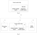
- Fig. 4 is a schematic diagram of a touch control chip provided by an embodiment of the present application. As shown in Fig. 4 , the touch control chip is integrated with static random access memory (SRAM) which includes a temporary variable region for temporarily storing a configuration file and a non-configuration file of the touch control chip in different time periods. That is, the configuration file and the non-configuration file can reuse the temporary variable region in different time periods. For example, during a time period 1, the temporary variable region temporarily stores the configuration file of the touch control chip, and during the time period 2, the temporary variable region temporarily stores the non-configuration file of the touch control chip, where the non-configuration file may include detected touch coordinates, etc.
- SRAM static random access memory
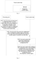
- FIG. 5 is an interaction flowchart of a method for processing a configuration file provided by another embodiment of the present application. As shown in Fig. 5 , the method includes the following process:
- Step S501 is the same as step S201, and the content and effect thereof are not described herein again.
- step S502 to step S504 when the processing unit acquires that the command region of the touch control chip is in an idle state and the temporary variable region is currently in an idle state, the processing unit sends a first command to the command region.
- the temporary variable region being currently in an idle state indicates that the temporary variable region is neither occupied by a configuration file nor occupied by a non-configuration file.
- the first command indicates that the processing unit is to write the configuration file to the touch control chip.
- the touch control chip stops the main loop and writes the second command into the command region, where the second command indicates waiting for the configuration file to be delivered.
- the processing unit delivers the configuration file to the touch control chip.
- the processing unit After the delivery is completed, the processing unit writes a third command to the command region, where the third command indicates that the configuration file has been delivered completely.
- the touch control chip After receiving the configuration file, the touch control chip stores the configuration file into the temporary variable region, parses the packet header, and determines whether the packet header has been completely received through the checksum of the packet header. When determining that the packet header has been completely received, the touch control chip then performs legality verification on the packet header. After determining that the packet header is legal, the touch control chip sequentially analyzes each first configuration module according to the number sequence of each first configuration module. As for each first configuration module, it is determined whether the first configuration module has been completely received through the module checksum of the first configuration module.
- the touch control chip When the first configuration module has been completely received, the touch control chip then performs the legality verification on the first configuration module. After all of the first configuration modules are verified to be legal, the touch control chip configures the parsed configuration file to each algorithm module of the touch control chip, and stores the parsed configuration file to the flash memory and deletes the configuration file in the temporary variable region for the non-profile to use the temporary variable region. The touch control chip continues to enter the main loop and writes a fourth command in the command region to clear the command region.
- the touch control chip since the touch control chip includes a temporary variable region, the configuration file is temporarily stored in the temporary variable region instead of being permanently stored in the variable region, thereby achieving the purpose of saving storage space. Further, since the temporary variable region can be reused by the configuration file and the non-configuration file, the utilization of the storage space can be improved.
- Fig. 6 is an interaction flowchart of a method for processing a configuration file provided by yet another embodiment of the present application. As shown in Fig. 6 , the method includes the following process:
- the processing unit when the processing unit acquires that the command region of the touch control chip is idle and the temporary variable region is currently in an idle state, the processing unit writes a read request to the command region.
- the temporary variable region being currently in an idle state indicates that the temporary variable region is neither occupied by a configuration file nor occupied by a non-configuration file.
- the read request may be a fifth command.
- the fifth command indicates that the processing unit is to read the configuration file parsed by the touch control chip, and the fifth command triggers the touch control chip to read the parsed configuration file from the flash memory, and stores the parsed configuration file in the temporary variable region.
- the touch control chip writes a sixth command to the command region, which indicates that the parsed configuration file required by the processing unit has been prepared.
- the processing unit reads the parsed configuration file from the temporary variable region and writes the forth command to the command region to clear the command region.
- the parsed configuration file is permanently stored in the flash memory, on the basis of this, when the processing unit needs to read the configuration file, it needs to send a read request to the touch control chip, so that the touch control chip reads the parsed configuration file from the flash memory to the temporary variable region according to the read request, thereby implementing that the processing unit reads the parsed configuration file.
- the present application temporarily stores the configuration file in a temporary variable region.
- First configuration modules included in the configuration file may be small.
- the present application can set a global variable region in a touch control chip.
- the global variable region may be used by at least one second configuration module which may be any updated first configuration module.
- Fig. 7 is an interaction flowchart of a method for processing a configuration file provided by still another embodiment of the present application. As shown in Fig. 7 , the method includes the following process.
- Step S701 a processing unit writes at least one second configuration module to a global variable region of a touch control chip.
- the processing unit When the processing unit acquires that the command region of the touch control chip is idle, the processing unit writes a seventh command to the command region which indicates that the processing unit is to write at least one second configuration module to the global variable region, and delivers the at least one second configuration module to the touch control chip. After receiving the command, the touch control chip stores the at least one second configuration module to the global variable region.
- the configuration flag of the packet header to which the at least one second configuration module belongs may be set to 1 when the processing chip writes the at least one second configuration module to the global variable region,.
- the configuration flag of the packet header to which at least one second configuration module belongs may be set to 0 when the processing chip writes the at least one second configuration module to the global variable region.
- Step S702 the touch control chip parses the at least one second configuration module and configures the parsed at least one second configuration module to at least one corresponding algorithm module of the touch control chip.
- the touch control chip determines whether the second configuration module has been completely received through the module checksum of the second configuration module. When the second configuration module has been completely received, the touch control chip performs legality verification on the second configuration module. After the second configuration module is verified to be legal, the touch control chip configures the parsed second configuration module to the corresponding algorithm module.
- Fig. 8 is a schematic diagram of a touch control chip provided by an embodiment of the present application.
- the SRAM further includes a global variable region.
- Storage space of the global variable region is smaller than that of the temporary variable region, and a starting storage address of the temporary variable region is smaller than a starting storage address of the global variable region.
- the storage space of the global variable region is less than 32 bytes, and the storage space of the temporary variable region is larger than 32 bytes.
- the temporary variable region since the temporary variable region is a reused temporary region, there are lots of interactive commands between the processing unit and the touch control chip.
- the global variable region set by the present application has a smaller storage space than the temporary variable region, thereby achieving the purpose of reducing the storage space. Further, since the second configuration module is permanently stored to the global variable region, there are fewer interaction commands between the processing unit and the touch control chip, thereby improving the updating efficiency of the configuration file.
- the method further includes: reading the second configuration module from the global variable region. Since the global variable region is dedicated to storing the second configuration module, the processing unit can directly read the second configuration module from the global variable region, thereby improving the reading efficiency of the configuration file.
- Fig. 9 is a schematic structural diagram of a touch device 90 provided by an embodiment of the present application.
- the device 90 may be a mobile phone, a notebook computer, a computer, a digital broadcast terminal, a messaging device, a game console, a tablet device, a medical device, a fitness device, a personal digital assistant, a kitchen appliance, a bathroom appliance, an air conditioner, and a lighting lamps or other smart terminals with a touch screen, a touch panel or a touch button.
- the device 90 includes a processing unit 91, a touch control chip 92 and a flash memory 93.
- the processing unit 91 may be an MCU, a CPU, a CPU or the like.
- the processing unit 91 is configured to determine a configuration file of the touch control chip and write the configuration file to the touch control chip.
- the configuration file includes a plurality of first configuration modules which are respectively configured to configure parameters of different attributes for the touch control chip.
- the touch control chip 92 is configured to parse the configuration file to obtain a parsed configuration file; and configure the parsed configuration file to each algorithm module of the touch control chip.
- the touch control chip 92 includes a temporary variable region 921 which is configured to temporarily store the configuration file and the non-configuration file of the touch control chip in different time periods, respectively; and the processing unit 91 is specifically configured to write the configuration file to the temporary variable region 921 when determining that the temporary variable region 921 is currently in an idle state.
- the touch control chip 92 is further configured to store the parsed configuration file to the flash memory 93 and delete the configuration file in the temporary variable region 921.
- the processing unit 91 is further configured to send a read request to the touch control chip 92 when determining that the temporary variable region 921 is currently in an idle state; and the touch control chip 92 is further configured to read the parsed configuration file from the flash memory 93 to the temporary variable region 921 according to the read request.
- the processing unit 91 is further configured to read the parsed configuration file from the temporary variable region 921.
- the touch control chip 92 further includes a global variable region 922 which is configured to store at least one second configuration module, where the at least one second configuration module is obtained after at least one corresponding first configuration module is updated; the processing unit 91 is further configured to write the at least one second configuration module to the global variable region 922; and the touch control chip 92 is further configured to parse the at least one second configuration module and configure the parsed at least one second configuration module to at least one corresponding algorithm module of the touch control chip.
- storage space of the global variable region 922 is smaller than storage space of the temporary variable region 921, and a starting storage address of the temporary variable region 921 is smaller than a starting storage address of the global variable region 922.
- the processing unit 91 is further configured to read the at least one second configuration module from the global variable region 922.
- the touch device provided by the embodiment of the present application can perform the method for processing a configuration file provided by the present application, and the implementation principle and technical effects thereof are similar, which are not described herein again.
- the application further provides a processing unit which may be an MCU, a CPU, a CPU or the like.
- the processing unit is configured to: determine a configuration file of a touch control chip; write the configuration file to the touch control chip; where the configuration file includes a plurality of first configuration modules which are respectively used for configuring parameters with different attributes for the touch control chip.
- the touch control chip includes a temporary variable region which is configured to temporarily store the configuration file and a non-configuration file of the touch control chip in different time periods, respectively; and the processing unit specifically configured to write the configuration file to the temporary variable region when determining that the temporary variable region is currently in an idle state.
- the processing unit is further configured to send a read request to the touch control chip when determining that the temporary variable region is currently in an idle state, so that the touch control chip reads the parsed configuration file from a flash memory to the temporary variable region according to the read request; and read the parsed configuration file from the temporary variable region.
- the touch control chip further includes a global variable region which is configured to store at least one second configuration module, where the at least one second configuration module is obtained after at least one corresponding first configuration module is updated; and the processing unit is further configured to write the at least one second configuration module to the global variable region.
- storage space of the global variable region is smaller than that of the temporary variable region, and a starting storage address of the temporary variable region is smaller than that of the global variable region.
- the processing unit is further configured to read the at least one second configuration module from the global variable region.
- the processing unit provided by the embodiment of the present application can perform a method for processing configuration file performed by the processing unit provided by the present application, and the implementation principle and technical effects thereof are similar, which are not described herein again.
- the present application further provides a touch control chip.
- the touch control chip is configured to: obtain a configuration file of the touch control chip; parse the configuration file to obtain a parsed configuration file; and configure the parsed configuration file to each algorithm module of the touch control chip; where the configuration file includes a plurality of first configuration modules which are respectively configured to configure parameters of different attributes for the touch control chip.
- the touch control chip includes a temporary variable region which is configured to temporarily store the configuration file and a non-configuration file of the touch control chip in different time periods, respectively; and the touch control chip is further configured to store the parsed configuration file to a flash memory and delete the configuration file in the temporary variable region.
- the touch control chip is further configured to receive a read request, and read the parsed configuration file from the flash memory to the temporary variable region according to the read request.
- the touch control chip further includes a global variable region which is configured to store at least one second configuration module, where the at least one second configuration module is obtained after at least one corresponding first configuration module is updated.
- the touch control chip is further configured to: obtain the at least one second configuration module; and parse the at least one second configuration module and configure the parsed at least one second configuration module to at least one corresponding algorithm module of the touch control chip.
- the storage space of the global variable region is smaller than that of the temporary variable region, and a starting storage address of the temporary variable region is smaller than that located in the global variable region.
- the touch control chip provided by the embodiment of the present application can perform the method for processing a configuration file executed by the touch control chip provided by the present application, and the implementation principle and technical effects thereof are similar, which are not described herein again.
- the above embodiments may be implemented in whole or in part by software, hardware, firmware, or any combination thereof.
- software When implemented by software, it may be implemented in whole or in part in the form of a computer program product.
- the computer program product includes one or more computer instructions.
- the computer program instructions When the computer program instructions are loaded and executed on a computer, the processes or functions described in accordance with the embodiments of the present invention are generated in whole or in part.
- the computer can be a general purpose computer, a special computer, a computer network, or other programmable devices.
- the computer instructions can be stored in a computer readable storage medium or transferred from one computer readable storage medium to another computer readable storage medium, for example, the computer instructions can be transferred from a website site, a computer, a server, a data center to another website site, computer, server, data center through wire (for example, coaxial cable, fiber optic, digital subscriber line (DSL) or wireless (for example, infrared, wireless, microwave).
- the computer readable storage medium can be any available media that can be accessed by a computer, or a data storage device such as a server, data center that includes one or more available media.
- the available medium may be a magnetic medium, such as a floppy disk, a hard disk, a magnetic tape, an optical medium, such as a DVD, or a semiconductor medium, such as a Solid State Disk (SSD) or the like.
- SSD Solid State Disk
Landscapes
- Engineering & Computer Science (AREA)
- Software Systems (AREA)
- Theoretical Computer Science (AREA)
- General Engineering & Computer Science (AREA)
- Physics & Mathematics (AREA)
- General Physics & Mathematics (AREA)
- Computer Security & Cryptography (AREA)
- Human Computer Interaction (AREA)
- User Interface Of Digital Computer (AREA)
- Information Retrieval, Db Structures And Fs Structures Therefor (AREA)
- Stored Programmes (AREA)
Claims (6)
- Ein Verfahren zum Verarbeiten einer Konfigurationsdatei, umfassend:- Erhalten der Konfigurationsdatei eines Touch-Control-Chips, wobei die Konfigurationsdatei eine Vielzahl von ersten Konfigurationsmodulen und einen Paketkopf mit einem Konfigurationsflag umfasst, wobei die Vielzahl der ersten Konfigurationsmodule jeweils zum Konfigurieren von Parametern verschiedener Attribute für den Touch-Control-Chip verwendet werden und das Konfigurationsflag anzeigt, dass die Konfigurationsdatei vollständig konfiguriert werden soll;- Parsen (S203, S503) der Konfigurationsdatei, um eine geparste Konfigurationsdatei zu erhalten; und- Konfigurieren (S204, S504) der geparsten Konfigurationsdatei für jedes Algorithmusmodul des Touch-Control-Chips;wobei der Touch-Control-Chip einen statischen Direktzugriffsspeicher umfasst, der einen globalen Variablenbereich umfasst und der globale Variablenbereich zum Speichern mindestens eines zweiten Konfigurationsmoduls verwendet wird, wobei das mindestens eine zweite Konfigurationsmodul erhalten wird, nachdem mindestens ein entsprechendes erstes Konfigurationsmodul aktualisiert wurde; unddas Verfahren ferner Folgendes umfasst:- Erhalten des mindestens einen zweiten Konfigurationsmoduls, wobei ein Konfigurationsflag eines Paketkopfes einer Konfigurationsdatei, zu der das mindestens eine zweite Konfigurationsmodul gehört, anzeigt, dass mindestens ein Konfigurationsmodul aktualisiert werden soll; und- Parsen (S702) des mindestens einen zweiten Konfigurationsmoduls und Konfigurieren des geparsten mindestens einen zweiten Konfigurationsmoduls für mindestens ein entsprechendes Algorithmusmodul des Touch-Control-Chips;wobei der statische Direktzugriffsspeicher des Touch-Control-Chips ferner einen temporären Variablenbereich umfasst, wobei der temporäre Variablenbereich zum temporären Speichern der Konfigurationsdatei bzw. einer Nicht-Konfigurationsdatei des Touch-Control-Chips in verschiedenen Zeiträumen verwendet wird;und nach dem Parsen (S203, S503) der Konfigurationsdatei, um die geparste Konfigurationsdatei zu erhalten, wobei das Verfahren ferner Folgendes umfasst:- Speichern (S504) der geparsten Konfigurationsdatei in einem Flash-Speicher und Löschen der Konfigurationsdatei in dem temporären Variablenbereich;wobei das Verfahren ferner Folgendes umfasst:- Empfangen einer Leseanforderung; und- Lesen (S602) der geparsten Konfigurationsdatei aus dem Flash-Speicher in den temporären Variablenbereich gemäß der Leseanforderung;wobei das Verfahren ferner Folgendes umfasst:- Lesen des zweiten Konfigurationsmoduls aus dem globalen Variablenbereich.
- Das Verfahren nach Anspruch 1, wobei der Speicherplatz des globalen Variablenbereichs kleiner ist als der Speicherplatz des temporären Variablenbereichs und eine Startspeicheradresse des temporären Variablenbereichs kleiner ist als eine Startspeicheradresse, die sich in dem globalen Variablenbereich befindet.
- Ein Touch-Control-Chip, wobei der Touch-Control-Chip konfiguriert ist, um:- Erhalten einer Konfigurationsdatei des Touch-Control-Chips, wobei die Konfigurationsdatei eine Vielzahl von ersten Konfigurationsmodulen und einen Paketkopf mit einem Konfigurationsflag umfasst, wobei die Vielzahl der ersten Konfigurationsmodule jeweils zum Konfigurieren von Parametern verschiedener Attribute für den Touch-Control-Chip verwendet werden und das Konfigurationsflag anzeigt, dass die Konfigurationsdatei vollständig konfiguriert werden soll;- Parsen der Konfigurationsdatei, um eine geparste Konfigurationsdatei zu erhalten; und- Konfigurieren der geparsten Konfigurationsdatei für jedes Algorithmusmodul des Touch-Control-Chips;wobei der Touch-Control-Chip ferner einen statischen Direktzugriffsspeicher umfasst, der einen globalen Variablenbereich umfasst und der globale Variablenbereich so konfiguriert ist, dass er mindestens ein zweites Konfigurationsmodul speichert, wobei das mindestens eine zweite Konfigurationsmodul erhalten wird, nachdem mindestens ein entsprechendes erstes Konfigurationsmodul aktualisiert wurde; und der Touch-Control-Chip ferner so konfiguriert ist, dass er:- Erhalten des mindestens einen zweiten Konfigurationsmoduls, wobei ein Konfigurationsflag eines Paketkopfes einer Konfigurationsdatei, zu der das mindestens eine zweite Konfigurationsmodul gehört, anzeigt, dass mindestens ein Konfigurationsmodul aktualisiert werden soll; und- Parsen des mindestens einen zweiten Konfigurationsmoduls und Konfigurieren des geparsten mindestens einen zweiten Konfigurationsmoduls an mindestens ein entsprechendes Algorithmusmodul des Touch-Control-Chips;wobei der statische Direktzugriffsspeicher des Touch-Control-Chips ferner einen temporären Variablenbereich umfasst, der so konfiguriert ist, dass er die Konfigurationsdatei und eine Nicht-Konfigurationsdatei des Touch-Control-Chips jeweils in verschiedenen Zeiträumen temporär speichert; und der Touch-Control-Chip ist ferner so konfiguriert, dass er:- Speichern der geparsten Konfigurationsdatei auf einem Flash-Speicher und Löschen der Konfigurationsdatei im temporären Variablenbereich;wobei der Touch-Control-Chip außerdem so konfiguriert ist, dass er:- Empfangen einer Leseanforderung; und- Lesen der geparsten Konfigurationsdatei aus dem Flash-Speicher in den temporären Variablenbereich gemäß der Leseanforderung;wobei der Touch-Control-Chip außerdem so konfiguriert ist, dass er das zweite Konfigurationsmodul aus dem globalen Variablenbereich liest.
- Der Touch-Control-Chip nach Anspruch 3, wobei der Speicherplatz des globalen Variablenbereichs kleiner ist als der Speicherplatz des temporären Variablenbereichs und eine Startspeicheradresse des temporären Variablenbereichs kleiner ist als eine Startspeicheradresse, die sich in dem globalen Variablenbereich befindet.
- Eine Touch-Vorrichtung, umfassend: einen Touch-Control-Chip nach Anspruch 3 oder 4.
- Ein Computerspeichermedium, das Computerbefehle enthält, die, wenn die Befehle von einem Computer ausgeführt werden, den Computer veranlassen, ein Verfahren nach Anspruch 1 oder 2 durchzuführen.
Applications Claiming Priority (1)
| Application Number | Priority Date | Filing Date | Title |
|---|---|---|---|
| PCT/CN2017/117529 WO2019119310A1 (zh) | 2017-12-20 | 2017-12-20 | 处理配置文件的方法、处理单元、触摸芯片、装置及介质 |
Publications (3)
| Publication Number | Publication Date |
|---|---|
| EP3550430A1 EP3550430A1 (de) | 2019-10-09 |
| EP3550430A4 EP3550430A4 (de) | 2019-12-25 |
| EP3550430B1 true EP3550430B1 (de) | 2023-07-26 |
Family
ID=66992904
Family Applications (1)
| Application Number | Title | Priority Date | Filing Date |
|---|---|---|---|
| EP17935049.1A Active EP3550430B1 (de) | 2017-12-20 | 2017-12-20 | Verfahren zur verarbeitung einer konfigurationsdatei, berührungschip, vorrichtung und medium |
Country Status (4)
| Country | Link |
|---|---|
| US (1) | US11237846B2 (de) |
| EP (1) | EP3550430B1 (de) |
| CN (1) | CN110998524B (de) |
| WO (1) | WO2019119310A1 (de) |
Families Citing this family (3)
| Publication number | Priority date | Publication date | Assignee | Title |
|---|---|---|---|---|
| TWI715371B (zh) * | 2019-12-25 | 2021-01-01 | 新唐科技股份有限公司 | 一次性可編程記憶體裝置及其容錯方法 |
| TWI719779B (zh) | 2019-12-26 | 2021-02-21 | 新唐科技股份有限公司 | 一次性可編程記憶體裝置及其容錯方法 |
| CN113900719B (zh) * | 2021-10-11 | 2025-03-21 | 京东方科技集团股份有限公司 | 触控芯片及其启动方法、触摸显示屏、主控芯片 |
Family Cites Families (14)
| Publication number | Priority date | Publication date | Assignee | Title |
|---|---|---|---|---|
| US20030074657A1 (en) * | 2001-10-12 | 2003-04-17 | Bramley Richard A. | Limited time evaluation system for firmware |
| US9354864B2 (en) * | 2008-05-08 | 2016-05-31 | Dialogic Corporation | Package header system and method to facilitate streaming a single firmware file upgrade |
| CN101452502B (zh) * | 2008-12-30 | 2011-04-13 | 华为技术有限公司 | 加载现场可编程门阵列fpga的方法、装置与系统 |
| KR20120041384A (ko) * | 2010-10-21 | 2012-05-02 | 삼성전자주식회사 | 모바일 디바이스의 펌웨어 업데이트 방법 및 장치 |
| CN102915284B (zh) * | 2012-11-14 | 2016-07-13 | 中航华东光电有限公司 | 红外触摸屏标准化配置方法 |
| US20140232672A1 (en) * | 2013-02-20 | 2014-08-21 | Tencent Technology (Shenzhen) Company Limited | Method and terminal for triggering application programs and application program functions |
| US9116774B2 (en) * | 2013-05-14 | 2015-08-25 | Sandisk Technologies Inc. | Firmware updates for multiple product configurations |
| US9552042B2 (en) * | 2013-08-02 | 2017-01-24 | Blackberry Limited | Electronic device and method of detecting touches on a touch-sensitive display |
| CN104765591A (zh) * | 2014-01-02 | 2015-07-08 | 腾讯科技(深圳)有限公司 | 一种软件配置参数更新的方法、终端服务器及系统 |
| US10372271B2 (en) * | 2014-07-18 | 2019-08-06 | Apple Inc. | Adjustment of touch sensing stimulation voltage levels based on touch performance |
| CN106168863A (zh) * | 2015-05-19 | 2016-11-30 | 义隆电子股份有限公司 | 具触控芯片的电脑装置及该触控芯片的更新方法 |
| CN105912265B (zh) * | 2016-04-01 | 2019-01-08 | 浪潮电子信息产业股份有限公司 | 一种Expander适配配置文件的方法及装置 |
| CN107037352B (zh) * | 2017-04-06 | 2020-01-17 | 芯海科技(深圳)股份有限公司 | 一种电容式触控按键芯片检测标定系统及方法 |
| CN107483556A (zh) * | 2017-07-25 | 2017-12-15 | 努比亚技术有限公司 | 一种远程配置方法、设备及计算机可读存储介质 |
-
2017
- 2017-12-20 WO PCT/CN2017/117529 patent/WO2019119310A1/zh not_active Ceased
- 2017-12-20 EP EP17935049.1A patent/EP3550430B1/de active Active
- 2017-12-20 CN CN201780002299.6A patent/CN110998524B/zh active Active
-
2019
- 2019-06-27 US US16/455,636 patent/US11237846B2/en active Active
Also Published As
| Publication number | Publication date |
|---|---|
| WO2019119310A1 (zh) | 2019-06-27 |
| EP3550430A4 (de) | 2019-12-25 |
| CN110998524B (zh) | 2024-05-28 |
| EP3550430A1 (de) | 2019-10-09 |
| CN110998524A (zh) | 2020-04-10 |
| US20190317778A1 (en) | 2019-10-17 |
| US11237846B2 (en) | 2022-02-01 |
Similar Documents
| Publication | Publication Date | Title |
|---|---|---|
| US20210132779A1 (en) | Electronic device and method for configuring display thereof | |
| CN112765271A (zh) | 区块链交易索引的存储方法、装置、计算机设备及介质 | |
| CN102411541B (zh) | 使用分开的读和写高速缓存的动态高速缓存配置 | |
| CN106708825B (zh) | 一种数据文件处理方法及系统 | |
| RU2617388C2 (ru) | Способ, терминал и электронное устройство для обработки документа электронной книги | |
| CN110221781B (zh) | 一种磁盘碎片的制造方法、装置、存储介质及智能终端 | |
| CN102981990A (zh) | 采用Android平台终端设备的数据传输方法及装置 | |
| US11237846B2 (en) | Method, processing unit, touch control chip, device and medium for processing configuration file | |
| US10198174B2 (en) | Electronic device and method of managing memory of electronic device | |
| US20170083261A1 (en) | Electronic device and method of analyzing fragmentation of electronic device | |
| WO2023066246A1 (zh) | 云手机安装应用的方法、系统和客户端云手机 | |
| CN107943505A (zh) | 应用升级管理方法、装置、存储介质及电子设备 | |
| CN109814980A (zh) | 镜像文件获取方法及装置 | |
| US10042856B2 (en) | Method and electronic device for processing data | |
| JP2016533588A (ja) | 記憶処理方法、装置及び端末 | |
| US10284614B2 (en) | Method for downloading contents of electronic device and electronic device thereof | |
| CN102664929A (zh) | 移动终端及其管理大容量存储设备的方法 | |
| CN105988803A (zh) | 一种应用程序显示的方法及终端 | |
| US20200051532A1 (en) | Image combination device and display system comprising the same | |
| CN106502750A (zh) | Ota升级方法及蓝牙芯片 | |
| CN103873631B (zh) | 一种移动终端来电界面显示的方法及装置 | |
| KR102443123B1 (ko) | 휴대단말기 제어방법 | |
| CN109542625A (zh) | 一种存储资源控制方法、装置及电子设备 | |
| CN114253691A (zh) | 基于操作系统的多卡自适应方法、装置和电子设备 | |
| CN115576942A (zh) | 一种数据处理方法、装置、设备和存储介质 |
Legal Events
| Date | Code | Title | Description |
|---|---|---|---|
| STAA | Information on the status of an ep patent application or granted ep patent |
Free format text: STATUS: UNKNOWN |
|
| STAA | Information on the status of an ep patent application or granted ep patent |
Free format text: STATUS: THE INTERNATIONAL PUBLICATION HAS BEEN MADE |
|
| PUAI | Public reference made under article 153(3) epc to a published international application that has entered the european phase |
Free format text: ORIGINAL CODE: 0009012 |
|
| STAA | Information on the status of an ep patent application or granted ep patent |
Free format text: STATUS: REQUEST FOR EXAMINATION WAS MADE |
|
| 17P | Request for examination filed |
Effective date: 20190627 |
|
| AK | Designated contracting states |
Kind code of ref document: A1 Designated state(s): AL AT BE BG CH CY CZ DE DK EE ES FI FR GB GR HR HU IE IS IT LI LT LU LV MC MK MT NL NO PL PT RO RS SE SI SK SM TR |
|
| AX | Request for extension of the european patent |
Extension state: BA ME |
|
| A4 | Supplementary search report drawn up and despatched |
Effective date: 20191125 |
|
| RIC1 | Information provided on ipc code assigned before grant |
Ipc: G06F 9/445 20180101AFI20191119BHEP Ipc: G06F 3/041 20060101ALI20191119BHEP |
|
| RIN1 | Information on inventor provided before grant (corrected) |
Inventor name: CHEN, YANRAN |
|
| DAV | Request for validation of the european patent (deleted) | ||
| DAX | Request for extension of the european patent (deleted) | ||
| STAA | Information on the status of an ep patent application or granted ep patent |
Free format text: STATUS: EXAMINATION IS IN PROGRESS |
|
| 17Q | First examination report despatched |
Effective date: 20210715 |
|
| GRAP | Despatch of communication of intention to grant a patent |
Free format text: ORIGINAL CODE: EPIDOSNIGR1 |
|
| STAA | Information on the status of an ep patent application or granted ep patent |
Free format text: STATUS: GRANT OF PATENT IS INTENDED |
|
| GRAS | Grant fee paid |
Free format text: ORIGINAL CODE: EPIDOSNIGR3 |
|
| GRAA | (expected) grant |
Free format text: ORIGINAL CODE: 0009210 |
|
| STAA | Information on the status of an ep patent application or granted ep patent |
Free format text: STATUS: THE PATENT HAS BEEN GRANTED |
|
| INTG | Intention to grant announced |
Effective date: 20230601 |
|
| AK | Designated contracting states |
Kind code of ref document: B1 Designated state(s): AL AT BE BG CH CY CZ DE DK EE ES FI FR GB GR HR HU IE IS IT LI LT LU LV MC MK MT NL NO PL PT RO RS SE SI SK SM TR |
|
| REG | Reference to a national code |
Ref country code: CH Ref legal event code: EP |
|
| REG | Reference to a national code |
Ref country code: DE Ref legal event code: R096 Ref document number: 602017072000 Country of ref document: DE |
|
| REG | Reference to a national code |
Ref country code: IE Ref legal event code: FG4D |
|
| REG | Reference to a national code |
Ref country code: LT Ref legal event code: MG9D |
|
| REG | Reference to a national code |
Ref country code: NL Ref legal event code: MP Effective date: 20230726 |
|
| REG | Reference to a national code |
Ref country code: AT Ref legal event code: MK05 Ref document number: 1592715 Country of ref document: AT Kind code of ref document: T Effective date: 20230726 |
|
| PG25 | Lapsed in a contracting state [announced via postgrant information from national office to epo] |
Ref country code: NL Free format text: LAPSE BECAUSE OF FAILURE TO SUBMIT A TRANSLATION OF THE DESCRIPTION OR TO PAY THE FEE WITHIN THE PRESCRIBED TIME-LIMIT Effective date: 20230726 |
|
| PG25 | Lapsed in a contracting state [announced via postgrant information from national office to epo] |
Ref country code: GR Free format text: LAPSE BECAUSE OF FAILURE TO SUBMIT A TRANSLATION OF THE DESCRIPTION OR TO PAY THE FEE WITHIN THE PRESCRIBED TIME-LIMIT Effective date: 20231027 |
|
| PG25 | Lapsed in a contracting state [announced via postgrant information from national office to epo] |
Ref country code: IS Free format text: LAPSE BECAUSE OF FAILURE TO SUBMIT A TRANSLATION OF THE DESCRIPTION OR TO PAY THE FEE WITHIN THE PRESCRIBED TIME-LIMIT Effective date: 20231126 |
|
| PG25 | Lapsed in a contracting state [announced via postgrant information from national office to epo] |
Ref country code: SE Free format text: LAPSE BECAUSE OF FAILURE TO SUBMIT A TRANSLATION OF THE DESCRIPTION OR TO PAY THE FEE WITHIN THE PRESCRIBED TIME-LIMIT Effective date: 20230726 Ref country code: RS Free format text: LAPSE BECAUSE OF FAILURE TO SUBMIT A TRANSLATION OF THE DESCRIPTION OR TO PAY THE FEE WITHIN THE PRESCRIBED TIME-LIMIT Effective date: 20230726 Ref country code: PT Free format text: LAPSE BECAUSE OF FAILURE TO SUBMIT A TRANSLATION OF THE DESCRIPTION OR TO PAY THE FEE WITHIN THE PRESCRIBED TIME-LIMIT Effective date: 20231127 Ref country code: NO Free format text: LAPSE BECAUSE OF FAILURE TO SUBMIT A TRANSLATION OF THE DESCRIPTION OR TO PAY THE FEE WITHIN THE PRESCRIBED TIME-LIMIT Effective date: 20231026 Ref country code: LV Free format text: LAPSE BECAUSE OF FAILURE TO SUBMIT A TRANSLATION OF THE DESCRIPTION OR TO PAY THE FEE WITHIN THE PRESCRIBED TIME-LIMIT Effective date: 20230726 Ref country code: LT Free format text: LAPSE BECAUSE OF FAILURE TO SUBMIT A TRANSLATION OF THE DESCRIPTION OR TO PAY THE FEE WITHIN THE PRESCRIBED TIME-LIMIT Effective date: 20230726 Ref country code: IS Free format text: LAPSE BECAUSE OF FAILURE TO SUBMIT A TRANSLATION OF THE DESCRIPTION OR TO PAY THE FEE WITHIN THE PRESCRIBED TIME-LIMIT Effective date: 20231126 Ref country code: HR Free format text: LAPSE BECAUSE OF FAILURE TO SUBMIT A TRANSLATION OF THE DESCRIPTION OR TO PAY THE FEE WITHIN THE PRESCRIBED TIME-LIMIT Effective date: 20230726 Ref country code: GR Free format text: LAPSE BECAUSE OF FAILURE TO SUBMIT A TRANSLATION OF THE DESCRIPTION OR TO PAY THE FEE WITHIN THE PRESCRIBED TIME-LIMIT Effective date: 20231027 Ref country code: FI Free format text: LAPSE BECAUSE OF FAILURE TO SUBMIT A TRANSLATION OF THE DESCRIPTION OR TO PAY THE FEE WITHIN THE PRESCRIBED TIME-LIMIT Effective date: 20230726 Ref country code: AT Free format text: LAPSE BECAUSE OF FAILURE TO SUBMIT A TRANSLATION OF THE DESCRIPTION OR TO PAY THE FEE WITHIN THE PRESCRIBED TIME-LIMIT Effective date: 20230726 |
|
| PG25 | Lapsed in a contracting state [announced via postgrant information from national office to epo] |
Ref country code: PL Free format text: LAPSE BECAUSE OF FAILURE TO SUBMIT A TRANSLATION OF THE DESCRIPTION OR TO PAY THE FEE WITHIN THE PRESCRIBED TIME-LIMIT Effective date: 20230726 |
|
| PG25 | Lapsed in a contracting state [announced via postgrant information from national office to epo] |
Ref country code: ES Free format text: LAPSE BECAUSE OF FAILURE TO SUBMIT A TRANSLATION OF THE DESCRIPTION OR TO PAY THE FEE WITHIN THE PRESCRIBED TIME-LIMIT Effective date: 20230726 |
|
| REG | Reference to a national code |
Ref country code: DE Ref legal event code: R097 Ref document number: 602017072000 Country of ref document: DE |
|
| PG25 | Lapsed in a contracting state [announced via postgrant information from national office to epo] |
Ref country code: SM Free format text: LAPSE BECAUSE OF FAILURE TO SUBMIT A TRANSLATION OF THE DESCRIPTION OR TO PAY THE FEE WITHIN THE PRESCRIBED TIME-LIMIT Effective date: 20230726 Ref country code: RO Free format text: LAPSE BECAUSE OF FAILURE TO SUBMIT A TRANSLATION OF THE DESCRIPTION OR TO PAY THE FEE WITHIN THE PRESCRIBED TIME-LIMIT Effective date: 20230726 Ref country code: ES Free format text: LAPSE BECAUSE OF FAILURE TO SUBMIT A TRANSLATION OF THE DESCRIPTION OR TO PAY THE FEE WITHIN THE PRESCRIBED TIME-LIMIT Effective date: 20230726 Ref country code: EE Free format text: LAPSE BECAUSE OF FAILURE TO SUBMIT A TRANSLATION OF THE DESCRIPTION OR TO PAY THE FEE WITHIN THE PRESCRIBED TIME-LIMIT Effective date: 20230726 Ref country code: DK Free format text: LAPSE BECAUSE OF FAILURE TO SUBMIT A TRANSLATION OF THE DESCRIPTION OR TO PAY THE FEE WITHIN THE PRESCRIBED TIME-LIMIT Effective date: 20230726 Ref country code: CZ Free format text: LAPSE BECAUSE OF FAILURE TO SUBMIT A TRANSLATION OF THE DESCRIPTION OR TO PAY THE FEE WITHIN THE PRESCRIBED TIME-LIMIT Effective date: 20230726 Ref country code: SK Free format text: LAPSE BECAUSE OF FAILURE TO SUBMIT A TRANSLATION OF THE DESCRIPTION OR TO PAY THE FEE WITHIN THE PRESCRIBED TIME-LIMIT Effective date: 20230726 |
|
| PG25 | Lapsed in a contracting state [announced via postgrant information from national office to epo] |
Ref country code: IT Free format text: LAPSE BECAUSE OF FAILURE TO SUBMIT A TRANSLATION OF THE DESCRIPTION OR TO PAY THE FEE WITHIN THE PRESCRIBED TIME-LIMIT Effective date: 20230726 |
|
| PLBE | No opposition filed within time limit |
Free format text: ORIGINAL CODE: 0009261 |
|
| STAA | Information on the status of an ep patent application or granted ep patent |
Free format text: STATUS: NO OPPOSITION FILED WITHIN TIME LIMIT |
|
| 26N | No opposition filed |
Effective date: 20240429 |
|
| PG25 | Lapsed in a contracting state [announced via postgrant information from national office to epo] |
Ref country code: SI Free format text: LAPSE BECAUSE OF FAILURE TO SUBMIT A TRANSLATION OF THE DESCRIPTION OR TO PAY THE FEE WITHIN THE PRESCRIBED TIME-LIMIT Effective date: 20230726 |
|
| REG | Reference to a national code |
Ref country code: CH Ref legal event code: PL |
|
| PG25 | Lapsed in a contracting state [announced via postgrant information from national office to epo] |
Ref country code: LU Free format text: LAPSE BECAUSE OF NON-PAYMENT OF DUE FEES Effective date: 20231220 |
|
| PG25 | Lapsed in a contracting state [announced via postgrant information from national office to epo] |
Ref country code: MC Free format text: LAPSE BECAUSE OF FAILURE TO SUBMIT A TRANSLATION OF THE DESCRIPTION OR TO PAY THE FEE WITHIN THE PRESCRIBED TIME-LIMIT Effective date: 20230726 |
|
| REG | Reference to a national code |
Ref country code: BE Ref legal event code: MM Effective date: 20231231 |
|
| PG25 | Lapsed in a contracting state [announced via postgrant information from national office to epo] |
Ref country code: MC Free format text: LAPSE BECAUSE OF FAILURE TO SUBMIT A TRANSLATION OF THE DESCRIPTION OR TO PAY THE FEE WITHIN THE PRESCRIBED TIME-LIMIT Effective date: 20230726 Ref country code: LU Free format text: LAPSE BECAUSE OF NON-PAYMENT OF DUE FEES Effective date: 20231220 |
|
| REG | Reference to a national code |
Ref country code: IE Ref legal event code: MM4A |
|
| PG25 | Lapsed in a contracting state [announced via postgrant information from national office to epo] |
Ref country code: IE Free format text: LAPSE BECAUSE OF NON-PAYMENT OF DUE FEES Effective date: 20231220 |
|
| PG25 | Lapsed in a contracting state [announced via postgrant information from national office to epo] |
Ref country code: BE Free format text: LAPSE BECAUSE OF NON-PAYMENT OF DUE FEES Effective date: 20231231 |
|
| PG25 | Lapsed in a contracting state [announced via postgrant information from national office to epo] |
Ref country code: FR Free format text: LAPSE BECAUSE OF NON-PAYMENT OF DUE FEES Effective date: 20231231 |
|
| PG25 | Lapsed in a contracting state [announced via postgrant information from national office to epo] |
Ref country code: CH Free format text: LAPSE BECAUSE OF NON-PAYMENT OF DUE FEES Effective date: 20231231 |
|
| PG25 | Lapsed in a contracting state [announced via postgrant information from national office to epo] |
Ref country code: IE Free format text: LAPSE BECAUSE OF NON-PAYMENT OF DUE FEES Effective date: 20231220 Ref country code: FR Free format text: LAPSE BECAUSE OF NON-PAYMENT OF DUE FEES Effective date: 20231231 Ref country code: CH Free format text: LAPSE BECAUSE OF NON-PAYMENT OF DUE FEES Effective date: 20231231 Ref country code: BE Free format text: LAPSE BECAUSE OF NON-PAYMENT OF DUE FEES Effective date: 20231231 |
|
| PG25 | Lapsed in a contracting state [announced via postgrant information from national office to epo] |
Ref country code: BG Free format text: LAPSE BECAUSE OF FAILURE TO SUBMIT A TRANSLATION OF THE DESCRIPTION OR TO PAY THE FEE WITHIN THE PRESCRIBED TIME-LIMIT Effective date: 20230726 |
|
| PG25 | Lapsed in a contracting state [announced via postgrant information from national office to epo] |
Ref country code: BG Free format text: LAPSE BECAUSE OF FAILURE TO SUBMIT A TRANSLATION OF THE DESCRIPTION OR TO PAY THE FEE WITHIN THE PRESCRIBED TIME-LIMIT Effective date: 20230726 |
|
| PG25 | Lapsed in a contracting state [announced via postgrant information from national office to epo] |
Ref country code: CY Free format text: LAPSE BECAUSE OF FAILURE TO SUBMIT A TRANSLATION OF THE DESCRIPTION OR TO PAY THE FEE WITHIN THE PRESCRIBED TIME-LIMIT; INVALID AB INITIO Effective date: 20171220 |
|
| PG25 | Lapsed in a contracting state [announced via postgrant information from national office to epo] |
Ref country code: HU Free format text: LAPSE BECAUSE OF FAILURE TO SUBMIT A TRANSLATION OF THE DESCRIPTION OR TO PAY THE FEE WITHIN THE PRESCRIBED TIME-LIMIT; INVALID AB INITIO Effective date: 20171220 |
|
| PG25 | Lapsed in a contracting state [announced via postgrant information from national office to epo] |
Ref country code: TR Free format text: LAPSE BECAUSE OF FAILURE TO SUBMIT A TRANSLATION OF THE DESCRIPTION OR TO PAY THE FEE WITHIN THE PRESCRIBED TIME-LIMIT Effective date: 20230726 |
|
| PGFP | Annual fee paid to national office [announced via postgrant information from national office to epo] |
Ref country code: DE Payment date: 20251216 Year of fee payment: 9 |
|
| PGFP | Annual fee paid to national office [announced via postgrant information from national office to epo] |
Ref country code: GB Payment date: 20251218 Year of fee payment: 9 |