EP3550411A1 - Touch sensor false detection prevention structure, and electronic device comprising same - Google Patents
Touch sensor false detection prevention structure, and electronic device comprising same Download PDFInfo
- Publication number
- EP3550411A1 EP3550411A1 EP17877409.7A EP17877409A EP3550411A1 EP 3550411 A1 EP3550411 A1 EP 3550411A1 EP 17877409 A EP17877409 A EP 17877409A EP 3550411 A1 EP3550411 A1 EP 3550411A1
- Authority
- EP
- European Patent Office
- Prior art keywords
- false detection
- touch sensor
- preventing structure
- touch
- hole
- Prior art date
- Legal status (The legal status is an assumption and is not a legal conclusion. Google has not performed a legal analysis and makes no representation as to the accuracy of the status listed.)
- Granted
Links
Images



Classifications
-
- G—PHYSICS
- G06—COMPUTING OR CALCULATING; COUNTING
- G06F—ELECTRIC DIGITAL DATA PROCESSING
- G06F3/00—Input arrangements for transferring data to be processed into a form capable of being handled by the computer; Output arrangements for transferring data from processing unit to output unit, e.g. interface arrangements
- G06F3/01—Input arrangements or combined input and output arrangements for interaction between user and computer
- G06F3/03—Arrangements for converting the position or the displacement of a member into a coded form
- G06F3/041—Digitisers, e.g. for touch screens or touch pads, characterised by the transducing means
- G06F3/0416—Control or interface arrangements specially adapted for digitisers
- G06F3/0418—Control or interface arrangements specially adapted for digitisers for error correction or compensation, e.g. based on parallax, calibration or alignment
-
- G—PHYSICS
- G06—COMPUTING OR CALCULATING; COUNTING
- G06F—ELECTRIC DIGITAL DATA PROCESSING
- G06F1/00—Details not covered by groups G06F3/00 - G06F13/00 and G06F21/00
- G06F1/16—Constructional details or arrangements
- G06F1/1613—Constructional details or arrangements for portable computers
- G06F1/1633—Constructional details or arrangements of portable computers not specific to the type of enclosures covered by groups G06F1/1615 - G06F1/1626
- G06F1/1637—Details related to the display arrangement, including those related to the mounting of the display in the housing
- G06F1/1643—Details related to the display arrangement, including those related to the mounting of the display in the housing the display being associated to a digitizer, e.g. laptops that can be used as penpads
-
- G—PHYSICS
- G06—COMPUTING OR CALCULATING; COUNTING
- G06F—ELECTRIC DIGITAL DATA PROCESSING
- G06F1/00—Details not covered by groups G06F3/00 - G06F13/00 and G06F21/00
- G06F1/16—Constructional details or arrangements
- G06F1/1613—Constructional details or arrangements for portable computers
- G06F1/1633—Constructional details or arrangements of portable computers not specific to the type of enclosures covered by groups G06F1/1615 - G06F1/1626
- G06F1/1656—Details related to functional adaptations of the enclosure, e.g. to provide protection against EMI, shock, water, or to host detachable peripherals like a mouse or removable expansions units like PCMCIA cards, or to provide access to internal components for maintenance or to removable storage supports like CDs or DVDs, or to mechanically mount accessories
-
- G—PHYSICS
- G06—COMPUTING OR CALCULATING; COUNTING
- G06F—ELECTRIC DIGITAL DATA PROCESSING
- G06F3/00—Input arrangements for transferring data to be processed into a form capable of being handled by the computer; Output arrangements for transferring data from processing unit to output unit, e.g. interface arrangements
- G06F3/01—Input arrangements or combined input and output arrangements for interaction between user and computer
- G06F3/03—Arrangements for converting the position or the displacement of a member into a coded form
- G06F3/033—Pointing devices displaced or positioned by the user, e.g. mice, trackballs, pens or joysticks; Accessories therefor
- G06F3/0354—Pointing devices displaced or positioned by the user, e.g. mice, trackballs, pens or joysticks; Accessories therefor with detection of two-dimensional [2D] relative movements between the device, or an operating part thereof, and a plane or surface, e.g. 2D mice, trackballs, pens or pucks
- G06F3/03547—Touch pads, in which fingers can move on a surface
-
- G—PHYSICS
- G06—COMPUTING OR CALCULATING; COUNTING
- G06F—ELECTRIC DIGITAL DATA PROCESSING
- G06F3/00—Input arrangements for transferring data to be processed into a form capable of being handled by the computer; Output arrangements for transferring data from processing unit to output unit, e.g. interface arrangements
- G06F3/01—Input arrangements or combined input and output arrangements for interaction between user and computer
- G06F3/03—Arrangements for converting the position or the displacement of a member into a coded form
- G06F3/041—Digitisers, e.g. for touch screens or touch pads, characterised by the transducing means
-
- G—PHYSICS
- G06—COMPUTING OR CALCULATING; COUNTING
- G06F—ELECTRIC DIGITAL DATA PROCESSING
- G06F3/00—Input arrangements for transferring data to be processed into a form capable of being handled by the computer; Output arrangements for transferring data from processing unit to output unit, e.g. interface arrangements
- G06F3/01—Input arrangements or combined input and output arrangements for interaction between user and computer
- G06F3/03—Arrangements for converting the position or the displacement of a member into a coded form
- G06F3/041—Digitisers, e.g. for touch screens or touch pads, characterised by the transducing means
- G06F3/0416—Control or interface arrangements specially adapted for digitisers
- G06F3/04164—Connections between sensors and controllers, e.g. routing lines between electrodes and connection pads
-
- H—ELECTRICITY
- H05—ELECTRIC TECHNIQUES NOT OTHERWISE PROVIDED FOR
- H05K—PRINTED CIRCUITS; CASINGS OR CONSTRUCTIONAL DETAILS OF ELECTRIC APPARATUS; MANUFACTURE OF ASSEMBLAGES OF ELECTRICAL COMPONENTS
- H05K1/00—Printed circuits
- H05K1/02—Details
- H05K1/0213—Electrical arrangements not otherwise provided for
- H05K1/0216—Reduction of cross-talk, noise or electromagnetic interference
- H05K1/0218—Reduction of cross-talk, noise or electromagnetic interference by printed shielding conductors, ground planes or power plane
-
- H—ELECTRICITY
- H05—ELECTRIC TECHNIQUES NOT OTHERWISE PROVIDED FOR
- H05K—PRINTED CIRCUITS; CASINGS OR CONSTRUCTIONAL DETAILS OF ELECTRIC APPARATUS; MANUFACTURE OF ASSEMBLAGES OF ELECTRICAL COMPONENTS
- H05K1/00—Printed circuits
- H05K1/02—Details
- H05K1/11—Printed elements for providing electric connections to or between printed circuits
Definitions
- the disclosures herein generally relate to a touch sensor false detection preventing structure and an electronic device having the same, and specifically relate to a touch sensor false detection preventing structure and an electronic device having the same that prevent a touch sensor from accidentally detecting a touch when the electronic device is moved while in operation.
- FIG. 1 is a schematic cross-sectional view illustrating a part of a conventional electronic device having a touch sensor.
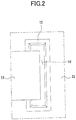
- FIG. 2 is a schematic plan view illustrating a through-hole and a sensor sheet in the related art illustrated in FIG. 1 .
- FIG. 3 is a schematic cross-sectional view illustrating an example in which, when a touch panel illustrated in FIG. 1 is in operation, the sensor sheet is moved and makes contact with the inner surface of the through-hole.
- a conventional electronic device 10 having a touch sensor includes a number of elements such as a touch panel 14 as illustrated in FIG. 1 .
- the conventional electronic device 10 includes a housing 11 provided with a through-hole provided area 15 through which a sensor sheet 13 passes, a circuit board 12 mounted inside the housing 11, and the touch panel 14 electrically connected to the circuit board 12 by the sensor sheet 13.
- the touch panel 14 is disposed above one side of the housing 11 in a vertically movable manner as desired, and a switching support 18 is disposed below the touch panel 14 and extends a predetermined length in a direction toward a switching member 17 that is mounted above the circuit board 12.
- the sensor sheet 13 is moved by the vertically movable touch panel 14. At this time, as illustrated in FIG. 3 , the sensor sheet 13 may come into contact with the inner surface of the through-hole provided area 15. In this case, the sensor sheet 13 may accidentally detect a touch, leading to a malfunction of the electronic device 10.
- a number of electrode patterns for detecting a touch signal are formed on the sensor sheet 13.
- the electrode patterns make contact with the inner surface of the through-hole provided area 15, an incorrect touch signal is generated.
- a touch sensor false detection preventing structure for use in an electric device.
- the electric device includes a housing that is provided with a through-hole provided area through which a sensor sheet passes, a circuit board that is mounted inside the housing, and a touch panel that is electrically connected to the circuit board by the sensor sheet.
- the touch sensor false detection preventing structure includes protruding portions formed on an inner surface at both ends of the through-hole provided area in planar view so as to protrude a predetermined distance, such that movement at a part of both side ends of the sensor sheet is restricted.
- a through-hole of the through-hole provided area has a rectangular shape in planar view and has a length corresponding to a width of the sensor sheet, and the protruding portions are formed at four corners of the through-hole in planar view.
- the sensor sheet includes two ground patterns formed on the respective side ends of the sensor sheet, and includes an electrode pattern formed between the two ground patterns and spaced a predetermined distance apart from the two ground patterns.
- the length of the protruding portions formed on the inner surface at the both ends of the through-hole provided area in planar view may include a predetermined length, so as to contact, at least in part, the ground patterns of the sensor sheet.
- the protruding portions may be spaced 1.0 mm to 2.0 mm apart from the electrode pattern of the sensor sheet.
- the touch panel is vertically movably disposed above one side of the housing, and a switching support is disposed below the touch panel to extend a predetermined length in a direction toward a switching member that is mounted above the circuit board.
- the through-hole provided area may be formed so as to extend a predetermined length in a direction perpendicular to an upper surface of the circuit board.
- the protruding portions formed on the inner surface at the both ends of the through-hole provided area in planar view may vertically extend to a length corresponding to an extension length of the through-hole.
- the length of the through-hole of the through-hole provided area may be from 105% to 115% of a width of the sensor sheet.
- the present invention may provide an electric device including the touch sensor false detection preventing structure.
- the through-hole provided area and the protruding portions having a specific structure are provided, thereby preventing the touch sensor from accidentally detecting a touch when the electronic device is moved while in operation.
- the ground patterns and the electrode pattern are provided at specific positions of the sensor sheet, and also the protruding portions are provided at specific positions of the through-hole, such that the protruding portions make contact with the ground patterns.
- the through-hole that extends the predetermined length in the direction perpendicular to the upper surface of the circuit board, and also the protruding portions are provided.
- the touch sensor false detection preventing structure by providing the touch sensor false detection preventing structure, it is possible to prevent the touch sensor from accidentally detecting a touch when the electronic device is moved while in operation.
- FIG. 4 is a schematic plan view illustrating a through-hole and a sensor sheet according to one embodiment of the present invention.
- FIG. 5 is a cross-sectional view taken through line A-A' of FIG. 4 .
- FIG. 6 is a cross-sectional view taken through line B-B' of FIG. 4 .
- a touch sensor false detection preventing structure 100 for use in an electronic device.
- the electronic device includes a housing 101 provided with a through-hole provided area 110 through which a sensor sheet 130 passes, a circuit board 102 mounted inside the housing 101, and a touch panel 103 electrically connected to the circuit board 102 by the sensor sheet 130.
- the touch sensor false detection preventing structure 100 the through-hole provided area 110 and protruding portions 120 having a specific structure are provided, thereby preventing a touch sensor from accidentally detecting a touch when the electronic device is moved while in operation.
- a through-hole 111 of the through-hole provided area 110 has a rectangular shape in planar view and has a length L corresponding to a width W of the sensor sheet 130. Further, the protruding portions 120 are preferably formed at the four corners of the through-hole 111 in planar view.
- the protruding portions 120 are formed on the inner surface at both ends 110a of the through-hole provided area 110 in planar view so as to protrude a predetermined distance F, such that the movement at a part of both side ends 130a of the sensor sheet 130 is restricted.
- the through-hole provided area 110 is formed so as to extend a predetermined length G in a direction perpendicular to the upper surface of the circuit board 120.
- the protruding portions 120 formed on the inner surface at the both ends 110a of the through-hole provided area 110 in planar view, may vertically extend to a length corresponding to the extension length G of the through-hole 111.
- the length L of the through-hole 111 of the through-hole provided area 110 is preferably from 105% to 115% of the width W of the sensor sheet 130. If the length L of the through-hole 111 exceeds 115% of the width W of the sensor sheet 130, the movement in the width direction of the sensor sheet 130 cannot be stably restricted, which is not preferable. Conversely, if the length L of the through-hole 111 is less than 105% of the width W of the sensor sheet 130, the movement in the width direction of the sensor sheet 130 is excessively restricted, causing the movement of the touch panel 103 to be restricted.
- FIG. 7 is a schematic plan view illustrating the through-hole, the sensor sheet, and ground patterns and electrode patterns formed on the sensor sheet according to the embodiment of the present invention.
- FIG. 8 is a schematic cross-sectional view illustrating a touch sensor false detection preventing structure according to the embodiment of the present invention.
- the sensor sheet 130 has a structure in which ground patterns (ground patterns) 131 and electrode patterns (electrode patterns) 132 are formed.
- the ground patterns 131 of the sensor sheet 130 are formed on the respective side ends of the sensor sheet 130, and the electrode patterns 132 are preferably formed between the two ground patterns 131, which are formed on the respective side ends of the sensor sheet 130, and are preferably spaced a predetermined distance apart from the two ground patterns 131.
- the length of the protruding portions 120 according to the present embodiment, formed on the inner surface at the both ends 110a of the through-hole provided area 110 in planar view, may include a predetermined length D, such that the protruding portions 120 may contact at least part of the ground patterns 131 of the sensor sheet 130.
- the protruding portions 120 may be preferably formed 1.0 mm to 2.0 mm (E) apart from the electrode patterns 132 of the sensor sheet 130.
- the touch sensor false detection preventing structure 100 may include the touch panel 103 vertically movably disposed above one side of the housing 101 as desired.
- the protruding portions 120 formed on the inner surface at the both ends 110a of the through-hole provided area 110 in planar view allow the electrode patterns 132 to be spaced a predetermined distance d apart from the inner surface of the through-hole 111 (see FIG. 6 ).
- the protruding portions 120 prevent contact between the electrode patterns 132 and the inner surface of the through-hole 111. Accordingly, accidental touch detection can be prevented.
- the electronic device having the touch sensor false detection preventing structure 100 according to the present embodiment may be provided.
- the through-hole provided area 110 and the protruding portions 120 having a specific structure can prevent the touch sensor from accidentally detecting a touch when the electronic device is moved.
- the ground patterns 131 and the electrode patterns 132 of the sensor sheet 130 are disposed at specific positions, and the protruding portions 120 of the through-hole 111 are disposed at specific positions, such that the protruding portions 120 make contact with the ground patterns 131.
- the electronic device is moved while in operation, it is possible to prevent contact between the electrode patterns 132 of the sensor sheet 130 and the inner surface of the through-hole 111. Accordingly, accidental touch detection can be prevented.
- the through-hole 111 that extends the predetermined length in the direction perpendicular to the upper surface of the circuit board 102 is provided, and the through-hole 111 is provided with the protruding portions 120.
- the touch sensor false detection preventing structure 100 of the present invention when the electronic device is moved while in operation, it is possible to prevent the touch sensor from accidentally detecting a touch.
Landscapes
- Engineering & Computer Science (AREA)
- Theoretical Computer Science (AREA)
- General Engineering & Computer Science (AREA)
- Physics & Mathematics (AREA)
- Human Computer Interaction (AREA)
- General Physics & Mathematics (AREA)
- Computer Hardware Design (AREA)
- Microelectronics & Electronic Packaging (AREA)
- Electromagnetism (AREA)
- Computer Networks & Wireless Communication (AREA)
- Position Input By Displaying (AREA)
- Switches That Are Operated By Magnetic Or Electric Fields (AREA)
Abstract
Description
- The disclosures herein generally relate to a touch sensor false detection preventing structure and an electronic device having the same, and specifically relate to a touch sensor false detection preventing structure and an electronic device having the same that prevent a touch sensor from accidentally detecting a touch when the electronic device is moved while in operation.
-
FIG. 1 is a schematic cross-sectional view illustrating a part of a conventional electronic device having a touch sensor.FIG. 2 is a schematic plan view illustrating a through-hole and a sensor sheet in the related art illustrated inFIG. 1 .FIG. 3 is a schematic cross-sectional view illustrating an example in which, when a touch panel illustrated inFIG. 1 is in operation, the sensor sheet is moved and makes contact with the inner surface of the through-hole. - A conventional
electronic device 10 having a touch sensor includes a number of elements such as atouch panel 14 as illustrated inFIG. 1 . - Specifically, the conventional
electronic device 10 includes ahousing 11 provided with a through-hole providedarea 15 through which asensor sheet 13 passes, acircuit board 12 mounted inside thehousing 11, and thetouch panel 14 electrically connected to thecircuit board 12 by thesensor sheet 13. - In the conventional
electronic device 10, thetouch panel 14 is disposed above one side of thehousing 11 in a vertically movable manner as desired, and aswitching support 18 is disposed below thetouch panel 14 and extends a predetermined length in a direction toward a switchingmember 17 that is mounted above thecircuit board 12. - In the above-described
electronic device 10, thesensor sheet 13 is moved by the verticallymovable touch panel 14. At this time, as illustrated inFIG. 3 , thesensor sheet 13 may come into contact with the inner surface of the through-hole providedarea 15. In this case, thesensor sheet 13 may accidentally detect a touch, leading to a malfunction of theelectronic device 10. - More specifically, a number of electrode patterns for detecting a touch signal are formed on the
sensor sheet 13. When the electrode patterns make contact with the inner surface of the through-hole providedarea 15, an incorrect touch signal is generated. - Accordingly, a technique that solves the above-described problem with the traditional electronic device having the touch sensor is desired.
- [PATENT DOCUMENT 1] Korean Laid-open Patent Publication No.
10-2006-0108999 - It is an object of the present invention to provide a touch sensor false detection preventing structure and an electronic device having the same that prevent the touch sensor from accidentally detecting a touch when the electronic device is moved while in operation.
- In order to achieve the above object, a touch sensor false detection preventing structure according to one aspect of the present invention for use in an electric device is provided. The electric device includes a housing that is provided with a through-hole provided area through which a sensor sheet passes, a circuit board that is mounted inside the housing, and a touch panel that is electrically connected to the circuit board by the sensor sheet. The touch sensor false detection preventing structure includes protruding portions formed on an inner surface at both ends of the through-hole provided area in planar view so as to protrude a predetermined distance, such that movement at a part of both side ends of the sensor sheet is restricted.
- In one embodiment of the present invention, a through-hole of the through-hole provided area has a rectangular shape in planar view and has a length corresponding to a width of the sensor sheet, and the protruding portions are formed at four corners of the through-hole in planar view.
- In one embodiment of the present invention, the sensor sheet includes two ground patterns formed on the respective side ends of the sensor sheet, and includes an electrode pattern formed between the two ground patterns and spaced a predetermined distance apart from the two ground patterns.
- Further, the length of the protruding portions formed on the inner surface at the both ends of the through-hole provided area in planar view may include a predetermined length, so as to contact, at least in part, the ground patterns of the sensor sheet.
- Further, the protruding portions may be spaced 1.0 mm to 2.0 mm apart from the electrode pattern of the sensor sheet.
- In one embodiment of the present invention, the touch panel is vertically movably disposed above one side of the housing, and a switching support is disposed below the touch panel to extend a predetermined length in a direction toward a switching member that is mounted above the circuit board.
- In one embodiment of the present invention, the through-hole provided area may be formed so as to extend a predetermined length in a direction perpendicular to an upper surface of the circuit board.
- Further, the protruding portions formed on the inner surface at the both ends of the through-hole provided area in planar view may vertically extend to a length corresponding to an extension length of the through-hole.
- In one embodiment of the present invention, the length of the through-hole of the through-hole provided area may be from 105% to 115% of a width of the sensor sheet.
- Further, the present invention may provide an electric device including the touch sensor false detection preventing structure.
- As described above, according to the touch sensor false detection preventing structure of the present invention, the through-hole provided area and the protruding portions having a specific structure are provided, thereby preventing the touch sensor from accidentally detecting a touch when the electronic device is moved while in operation.
- Further, according to the touch sensor false detection preventing structure of the present invention, the ground patterns and the electrode pattern are provided at specific positions of the sensor sheet, and also the protruding portions are provided at specific positions of the through-hole, such that the protruding portions make contact with the ground patterns. With the above configuration, it is possible to prevent the electrode pattern of the sensor sheet from contacting the inner surface of the through-hole. As a result, accidental touch detection can be prevented.
- Further, according to the touch sensor false detection preventing structure of the present invention, the through-hole that extends the predetermined length in the direction perpendicular to the upper surface of the circuit board, and also the protruding portions are provided. With the above configuration, it is possible to prevent the electrode pattern formed on the sensor sheet from contacting the inner surface of the through-hole. As a result, accidental touch detection can be prevented.
- Further, according to the electronic device of the present invention, by providing the touch sensor false detection preventing structure, it is possible to prevent the touch sensor from accidentally detecting a touch when the electronic device is moved while in operation.
-
-
FIG. 1 is a schematic cross-sectional view illustrating a part of a conventional electronic device having a touch sensor; -
FIG. 2 is a schematic plan view illustrating a through-hole and a sensor sheet in the related art illustrated inFIG. 1 ; -
FIG. 3 is a schematic cross-sectional view illustrating an example in which, when a touch panel illustrated inFIG. 1 is in operation, the sensor sheet is moved and makes contact with the inner surface of the through-hole; -
FIG. 4 is a schematic plan view illustrating a through-hole and a sensor sheet according to one embodiment of the present invention; -
FIG. 5 is a cross-sectional view taken through line A-A' ofFIG. 4 ; -
FIG. 6 is a cross-sectional view taken through line B-B' ofFIG. 4 ; -
FIG. 7 is a schematic plan view illustrating the through-hole, the sensor sheet, and ground patterns and electrode patterns formed on the sensor sheet according to the embodiment of the present invention; and -
FIG. 8 is a schematic cross-sectional view illustrating a touch sensor false detection preventing structure according to the embodiment of the present invention. - In the following, embodiments of the present invention will be described with reference to the accompanying drawings.
- First, terms used herein and in the claims should not be restrictively interpreted as ordinary meanings or dictionary-based meanings, and should be interpreted as meanings conforming to the technical ideas of the present invention.
- It should be noted that when a member is described herein as being provided "on" another member, this means not only that the member is in contact with the other member, but that an additional member is interposed between the two members. Further, when a member is described herein as "including" an element, this does not mean that other elements are excluded, and means that other elements may be further included, unless stated to the contrary.
-
FIG. 4 is a schematic plan view illustrating a through-hole and a sensor sheet according to one embodiment of the present invention.FIG. 5 is a cross-sectional view taken through line A-A' ofFIG. 4 .FIG. 6 is a cross-sectional view taken through line B-B' ofFIG. 4 . - Referring to these drawings, a touch sensor false
detection preventing structure 100 according to the present embodiment for use in an electronic device is provided. The electronic device includes ahousing 101 provided with a through-hole providedarea 110 through which asensor sheet 130 passes, acircuit board 102 mounted inside thehousing 101, and atouch panel 103 electrically connected to thecircuit board 102 by thesensor sheet 130. In the touch sensor falsedetection preventing structure 100, the through-hole providedarea 110 and protrudingportions 120 having a specific structure are provided, thereby preventing a touch sensor from accidentally detecting a touch when the electronic device is moved while in operation. - In the following, each element configuring the touch sensor false
detection preventing structure 100 according to the present embodiment will be described in detail with reference to the drawings. - A through-
hole 111 of the through-hole providedarea 110 according to the present embodiment has a rectangular shape in planar view and has a length L corresponding to a width W of thesensor sheet 130. Further, theprotruding portions 120 are preferably formed at the four corners of the through-hole 111 in planar view. - The
protruding portions 120 according to the present embodiment are formed on the inner surface at bothends 110a of the through-hole providedarea 110 in planar view so as to protrude a predetermined distance F, such that the movement at a part of bothside ends 130a of thesensor sheet 130 is restricted. - Further, the through-hole provided
area 110 is formed so as to extend a predetermined length G in a direction perpendicular to the upper surface of thecircuit board 120. - Further, the protruding
portions 120, formed on the inner surface at the both ends 110a of the through-hole providedarea 110 in planar view, may vertically extend to a length corresponding to the extension length G of the through-hole 111. - Further, as illustrated in
FIG. 4 , the length L of the through-hole 111 of the through-hole providedarea 110 is preferably from 105% to 115% of the width W of thesensor sheet 130. If the length L of the through-hole 111 exceeds 115% of the width W of thesensor sheet 130, the movement in the width direction of thesensor sheet 130 cannot be stably restricted, which is not preferable. Conversely, if the length L of the through-hole 111 is less than 105% of the width W of thesensor sheet 130, the movement in the width direction of thesensor sheet 130 is excessively restricted, causing the movement of thetouch panel 103 to be restricted. -
FIG. 7 is a schematic plan view illustrating the through-hole, the sensor sheet, and ground patterns and electrode patterns formed on the sensor sheet according to the embodiment of the present invention.FIG. 8 is a schematic cross-sectional view illustrating a touch sensor false detection preventing structure according to the embodiment of the present invention. - Referring to
FIGS. 7 and8 together withFIGS. 4 through 6 , thesensor sheet 130 according to the present embodiment has a structure in which ground patterns (ground patterns) 131 and electrode patterns (electrode patterns) 132 are formed. - Specifically, as illustrated in
FIG. 7 , theground patterns 131 of thesensor sheet 130 are formed on the respective side ends of thesensor sheet 130, and theelectrode patterns 132 are preferably formed between the twoground patterns 131, which are formed on the respective side ends of thesensor sheet 130, and are preferably spaced a predetermined distance apart from the twoground patterns 131. - Further, as illustrated in
FIG. 4 andFIG. 7 , the length of the protrudingportions 120 according to the present embodiment, formed on the inner surface at the both ends 110a of the through-hole providedarea 110 in planar view, may include a predetermined length D, such that the protrudingportions 120 may contact at least part of theground patterns 131 of thesensor sheet 130. - Further, as illustrated in
FIG. 7 , the protrudingportions 120 according to the present embodiment may be preferably formed 1.0 mm to 2.0 mm (E) apart from theelectrode patterns 132 of thesensor sheet 130. - As illustrated in
FIG. 8 , the touch sensor falsedetection preventing structure 100 according to the present embodiment may include thetouch panel 103 vertically movably disposed above one side of thehousing 101 as desired. - In this case, by disposing a
switching support 105 below thetouch panel 103 to extend a predetermined length in a direction toward a switchingmember 104 mounted above thecircuit board 102, a push operation in the vertical direction is achieved. - The protruding
portions 120 formed on the inner surface at the both ends 110a of the through-hole providedarea 110 in planar view allow theelectrode patterns 132 to be spaced a predetermined distance d apart from the inner surface of the through-hole 111 (seeFIG. 6 ). Thus, when the push operation is performed in accordance with the user's intention, and thereby thetouch panel 103 is moved, the protrudingportions 120 prevent contact between theelectrode patterns 132 and the inner surface of the through-hole 111. Accordingly, accidental touch detection can be prevented. - Further, the electronic device having the touch sensor false
detection preventing structure 100 according to the present embodiment may be provided. - As described above, according to the touch sensor false
detection preventing structure 100 of the present invention, the through-hole providedarea 110 and the protrudingportions 120 having a specific structure can prevent the touch sensor from accidentally detecting a touch when the electronic device is moved. - Further, according to the touch sensor false
detection preventing structure 100 of the present invention, theground patterns 131 and theelectrode patterns 132 of thesensor sheet 130 are disposed at specific positions, and the protrudingportions 120 of the through-hole 111 are disposed at specific positions, such that the protrudingportions 120 make contact with theground patterns 131. Thus, even if the electronic device is moved while in operation, it is possible to prevent contact between theelectrode patterns 132 of thesensor sheet 130 and the inner surface of the through-hole 111. Accordingly, accidental touch detection can be prevented. - Further, according to the touch sensor false
detection preventing structure 100 of the present invention, the through-hole 111 that extends the predetermined length in the direction perpendicular to the upper surface of thecircuit board 102 is provided, and the through-hole 111 is provided with the protrudingportions 120. With the above configuration, it is possible to prevent theelectrode patterns 132 formed on thesensor sheet 130 from making contact with the inner surface of the through-hole 111. Accordingly, accidental touch detection can be prevented. - Further, according to the touch sensor false
detection preventing structure 100 of the present invention, when the electronic device is moved while in operation, it is possible to prevent the touch sensor from accidentally detecting a touch. - Although the present invention has been described with reference to the embodiments, the present invention is not limited to the above-described embodiments. Various variations and modifications may be made without departing from the scope of the present invention.
- The present application is based on and claims priority to Korean patent application No.
10-2016-0164165 filed on December 5, 2016 -
- 10
- conventional electronic device
- 11
- housing
- 12
- circuit board
- 13
- sensor sheet
- 14
- touch panel
- 15
- through-hole provided area
- 16
- through-hole
- 17
- switching member
- 18
- switching support
- 100
- touch sensor false detection preventing structure
- 101
- housing
- 102
- circuit board
- 103
- touch panel
- 104
- switching member
- 105
- switching support
- 110
- through-hole provided area
- 110a
- both ends
- 111
- through-hole
- 120
- protruding portion
- 130
- sensor sheet
- 130a
- both side ends
- 131
- ground patterns
- 132
- electrode pattern
Claims (10)
- A touch sensor false detection preventing structure for use in an electronic device including a housing that is provided with a through-hole provided area through which a sensor sheet passes, a circuit board that is mounted inside the housing, and a touch panel that is electrically connected to the circuit board by the sensor sheet, the touch sensor false detection preventing structure comprising,
protruding portions formed on an inner surface at both ends of the through-hole provided area in planar view so as to protrude a predetermined distance, such that movement at a part of both side ends of the sensor sheet is restricted. - The touch sensor false detection preventing structure according to claim 1, wherein a through-hole of the through-hole provided area has a rectangular shape in planar view and has a length corresponding to a width of the sensor sheet, and
the protruding portions are formed at four corners of the through-hole in planar view. - The touch sensor false detection preventing structure according to claim 1, wherein the sensor sheet includes
two ground patterns formed on the respective side ends of the sensor sheet, and
an electrode pattern formed between the two ground patterns and spaced a predetermined distance apart from the two ground patterns. - The touch sensor false detection preventing structure according to claim 3, wherein a length of the protruding portions formed on the inner surface at the both ends of the through-hole provided area in planar view includes a predetermined length, so as to contact, at least in part, the respective ground patterns of the sensor sheet.
- The touch sensor false detection preventing structure according to claim 4, wherein the protruding portions are spaced 1.0 mm to 2.0 mm apart from the electrode pattern of the sensor sheet.
- The touch sensor false detection preventing structure according to claim 1, wherein the touch panel is vertically movably disposed above one side of the housing, and a switching support is disposed below the touch panel to extend a predetermined length in a direction toward a switching member that is mounted above the circuit board.
- The touch sensor false detection preventing structure according to claim 1, wherein the through-hole provided area is formed so as to extend a predetermined length in a direction perpendicular to an upper surface of the circuit board.
- The touch sensor false detection preventing structure according to claim 7, wherein the protruding portions formed on the inner surface at the both ends of the through-hole provided area in planar view vertically extend to a length corresponding to an extension length of a through-hole.
- The touch sensor false detection preventing structure according to claim 1, wherein a length of a through-hole of the through-hole provided area is from 105% to 115% of a width of the sensor sheet.
- The electronic device including the touch sensor false detection preventing structure according to any one of claims 1 to 9.
Applications Claiming Priority (2)
| Application Number | Priority Date | Filing Date | Title |
|---|---|---|---|
| KR1020160164165A KR101752767B1 (en) | 2016-12-05 | 2016-12-05 | Detecting Error Preventive Structure for Touch Sensor, and Electric Device Having The Same |
| PCT/JP2017/040499 WO2018105305A1 (en) | 2016-12-05 | 2017-11-09 | Touch sensor false detection prevention structure, and electronic device comprising same |
Publications (3)
| Publication Number | Publication Date |
|---|---|
| EP3550411A1 true EP3550411A1 (en) | 2019-10-09 |
| EP3550411A4 EP3550411A4 (en) | 2020-07-08 |
| EP3550411B1 EP3550411B1 (en) | 2021-04-28 |
Family
ID=59279405
Family Applications (1)
| Application Number | Title | Priority Date | Filing Date |
|---|---|---|---|
| EP17877409.7A Active EP3550411B1 (en) | 2016-12-05 | 2017-11-09 | Touch sensor false detection prevention structure, and electronic device comprising same |
Country Status (6)
| Country | Link |
|---|---|
| US (1) | US10838552B2 (en) |
| EP (1) | EP3550411B1 (en) |
| JP (1) | JP6765440B2 (en) |
| KR (1) | KR101752767B1 (en) |
| CN (1) | CN110023890B (en) |
| WO (1) | WO2018105305A1 (en) |
Families Citing this family (1)
| Publication number | Priority date | Publication date | Assignee | Title |
|---|---|---|---|---|
| WO2023223632A1 (en) | 2022-05-18 | 2023-11-23 | アルプスアルパイン株式会社 | Input device and assembly method |
Family Cites Families (12)
| Publication number | Priority date | Publication date | Assignee | Title |
|---|---|---|---|---|
| KR100641199B1 (en) | 2005-04-14 | 2006-11-06 | 엘지전자 주식회사 | Portable terminal with touch screen malfunction prevention device |
| JP2008071239A (en) * | 2006-09-15 | 2008-03-27 | Alps Electric Co Ltd | Input device |
| KR101670258B1 (en) * | 2009-07-06 | 2016-10-31 | 삼성전자 주식회사 | Mobile device having flexible printed circuit board |
| JP5886489B2 (en) * | 2009-09-21 | 2016-03-16 | 株式会社ワコム | Position detection device |
| US8611077B2 (en) * | 2010-08-27 | 2013-12-17 | Apple Inc. | Electronic devices with component mounting structures |
| KR101822657B1 (en) * | 2011-06-24 | 2018-03-09 | 엘지디스플레이 주식회사 | Liquid crystal display device |
| JP5871307B2 (en) * | 2011-09-30 | 2016-03-01 | 株式会社ワコム | Position detection sensor unit and position detection device |
| JP5868721B2 (en) * | 2012-02-10 | 2016-02-24 | ホシデン株式会社 | Input device |
| WO2014192336A1 (en) * | 2013-05-29 | 2014-12-04 | シャープ株式会社 | Touch panel substrate |
| KR102345612B1 (en) * | 2015-07-08 | 2022-01-03 | 삼성디스플레이 주식회사 | Display device |
| US9851837B2 (en) * | 2015-12-28 | 2017-12-26 | Olympus Scientific Solutions Americas, Inc. | Touchscreen display assembly for harsh environment |
| WO2017142870A1 (en) * | 2016-02-15 | 2017-08-24 | Neocoil, Llc | Magnetic resonance imaging compatible mobile computing device |
-
2016
- 2016-12-05 KR KR1020160164165A patent/KR101752767B1/en active Active
-
2017
- 2017-11-09 WO PCT/JP2017/040499 patent/WO2018105305A1/en not_active Ceased
- 2017-11-09 EP EP17877409.7A patent/EP3550411B1/en active Active
- 2017-11-09 CN CN201780074515.8A patent/CN110023890B/en active Active
- 2017-11-09 JP JP2018554876A patent/JP6765440B2/en active Active
-
2019
- 2019-05-09 US US16/407,402 patent/US10838552B2/en active Active
Also Published As
| Publication number | Publication date |
|---|---|
| JP6765440B2 (en) | 2020-10-07 |
| CN110023890B (en) | 2022-04-01 |
| US20190265838A1 (en) | 2019-08-29 |
| KR101752767B1 (en) | 2017-06-30 |
| EP3550411A4 (en) | 2020-07-08 |
| US10838552B2 (en) | 2020-11-17 |
| CN110023890A (en) | 2019-07-16 |
| EP3550411B1 (en) | 2021-04-28 |
| WO2018105305A1 (en) | 2018-06-14 |
| JPWO2018105305A1 (en) | 2019-07-11 |
Similar Documents
| Publication | Publication Date | Title |
|---|---|---|
| JP4554651B2 (en) | Touch panel input device | |
| EP2741064B1 (en) | Capacitive Tactile Sensor | |
| KR20140135708A (en) | Inductive touch sensor using a flexible coil | |
| US10042455B2 (en) | Detecting sensor having position detection and pressing force detection electrodes | |
| US7282656B2 (en) | Slide switch | |
| KR101905851B1 (en) | Capacitive switch | |
| JP4912428B2 (en) | Vibration detection switch | |
| CN106662942A (en) | Display unit with touch panel | |
| US20130319837A1 (en) | Press key | |
| CA2609862A1 (en) | Switch assembly and associated handheld electronic device | |
| US20060131158A1 (en) | Membrane switch | |
| US10838552B2 (en) | Touch sensor false detection preventing structure and electronic device having same | |
| EP3582243B1 (en) | Four-way switch including malfunction prevention structure | |
| US10338509B2 (en) | Information inputting apparatus and image forming apparatus having information inputting apparatus | |
| JPH0554205B2 (en) | ||
| JP2007122891A (en) | Touch keys and electrical equipment using them | |
| KR101032995B1 (en) | Signal input device for electronic products | |
| CN203812776U (en) | Key bonding pad, key, key switch, and portable device | |
| JP6230119B2 (en) | Input device | |
| KR101998362B1 (en) | Proximity sensor with multiple electrodes | |
| JP2007173067A (en) | Switch device with touch detection function | |
| JP2005197038A (en) | Switch with fingerprint authentication function | |
| KR101852421B1 (en) | Switch apparatus | |
| JP2017195062A (en) | Input switch and electronic apparatus | |
| JP5806375B2 (en) | Input device and portable terminal |
Legal Events
| Date | Code | Title | Description |
|---|---|---|---|
| STAA | Information on the status of an ep patent application or granted ep patent |
Free format text: STATUS: THE INTERNATIONAL PUBLICATION HAS BEEN MADE |
|
| PUAI | Public reference made under article 153(3) epc to a published international application that has entered the european phase |
Free format text: ORIGINAL CODE: 0009012 |
|
| STAA | Information on the status of an ep patent application or granted ep patent |
Free format text: STATUS: REQUEST FOR EXAMINATION WAS MADE |
|
| 17P | Request for examination filed |
Effective date: 20190515 |
|
| AK | Designated contracting states |
Kind code of ref document: A1 Designated state(s): AL AT BE BG CH CY CZ DE DK EE ES FI FR GB GR HR HU IE IS IT LI LT LU LV MC MK MT NL NO PL PT RO RS SE SI SK SM TR |
|
| AX | Request for extension of the european patent |
Extension state: BA ME |
|
| DAV | Request for validation of the european patent (deleted) | ||
| DAX | Request for extension of the european patent (deleted) | ||
| A4 | Supplementary search report drawn up and despatched |
Effective date: 20200608 |
|
| RIC1 | Information provided on ipc code assigned before grant |
Ipc: H05K 1/02 20060101ALI20200602BHEP Ipc: G06F 3/041 20060101AFI20200602BHEP Ipc: G06F 3/0354 20130101ALI20200602BHEP Ipc: G06F 1/16 20060101ALI20200602BHEP |
|
| GRAP | Despatch of communication of intention to grant a patent |
Free format text: ORIGINAL CODE: EPIDOSNIGR1 |
|
| STAA | Information on the status of an ep patent application or granted ep patent |
Free format text: STATUS: GRANT OF PATENT IS INTENDED |
|
| INTG | Intention to grant announced |
Effective date: 20210202 |
|
| GRAS | Grant fee paid |
Free format text: ORIGINAL CODE: EPIDOSNIGR3 |
|
| GRAA | (expected) grant |
Free format text: ORIGINAL CODE: 0009210 |
|
| STAA | Information on the status of an ep patent application or granted ep patent |
Free format text: STATUS: THE PATENT HAS BEEN GRANTED |
|
| AK | Designated contracting states |
Kind code of ref document: B1 Designated state(s): AL AT BE BG CH CY CZ DE DK EE ES FI FR GB GR HR HU IE IS IT LI LT LU LV MC MK MT NL NO PL PT RO RS SE SI SK SM TR |
|
| REG | Reference to a national code |
Ref country code: GB Ref legal event code: FG4D |
|
| REG | Reference to a national code |
Ref country code: CH Ref legal event code: EP |
|
| REG | Reference to a national code |
Ref country code: AT Ref legal event code: REF Ref document number: 1387832 Country of ref document: AT Kind code of ref document: T Effective date: 20210515 |
|
| REG | Reference to a national code |
Ref country code: DE Ref legal event code: R096 Ref document number: 602017037838 Country of ref document: DE |
|
| REG | Reference to a national code |
Ref country code: IE Ref legal event code: FG4D |
|
| REG | Reference to a national code |
Ref country code: LT Ref legal event code: MG9D |
|
| REG | Reference to a national code |
Ref country code: AT Ref legal event code: MK05 Ref document number: 1387832 Country of ref document: AT Kind code of ref document: T Effective date: 20210428 |
|
| PG25 | Lapsed in a contracting state [announced via postgrant information from national office to epo] |
Ref country code: FI Free format text: LAPSE BECAUSE OF FAILURE TO SUBMIT A TRANSLATION OF THE DESCRIPTION OR TO PAY THE FEE WITHIN THE PRESCRIBED TIME-LIMIT Effective date: 20210428 Ref country code: LT Free format text: LAPSE BECAUSE OF FAILURE TO SUBMIT A TRANSLATION OF THE DESCRIPTION OR TO PAY THE FEE WITHIN THE PRESCRIBED TIME-LIMIT Effective date: 20210428 Ref country code: BG Free format text: LAPSE BECAUSE OF FAILURE TO SUBMIT A TRANSLATION OF THE DESCRIPTION OR TO PAY THE FEE WITHIN THE PRESCRIBED TIME-LIMIT Effective date: 20210728 Ref country code: AT Free format text: LAPSE BECAUSE OF FAILURE TO SUBMIT A TRANSLATION OF THE DESCRIPTION OR TO PAY THE FEE WITHIN THE PRESCRIBED TIME-LIMIT Effective date: 20210428 Ref country code: HR Free format text: LAPSE BECAUSE OF FAILURE TO SUBMIT A TRANSLATION OF THE DESCRIPTION OR TO PAY THE FEE WITHIN THE PRESCRIBED TIME-LIMIT Effective date: 20210428 Ref country code: NL Free format text: LAPSE BECAUSE OF FAILURE TO SUBMIT A TRANSLATION OF THE DESCRIPTION OR TO PAY THE FEE WITHIN THE PRESCRIBED TIME-LIMIT Effective date: 20210428 |
|
| PG25 | Lapsed in a contracting state [announced via postgrant information from national office to epo] |
Ref country code: RS Free format text: LAPSE BECAUSE OF FAILURE TO SUBMIT A TRANSLATION OF THE DESCRIPTION OR TO PAY THE FEE WITHIN THE PRESCRIBED TIME-LIMIT Effective date: 20210428 Ref country code: SE Free format text: LAPSE BECAUSE OF FAILURE TO SUBMIT A TRANSLATION OF THE DESCRIPTION OR TO PAY THE FEE WITHIN THE PRESCRIBED TIME-LIMIT Effective date: 20210428 Ref country code: PT Free format text: LAPSE BECAUSE OF FAILURE TO SUBMIT A TRANSLATION OF THE DESCRIPTION OR TO PAY THE FEE WITHIN THE PRESCRIBED TIME-LIMIT Effective date: 20210830 Ref country code: PL Free format text: LAPSE BECAUSE OF FAILURE TO SUBMIT A TRANSLATION OF THE DESCRIPTION OR TO PAY THE FEE WITHIN THE PRESCRIBED TIME-LIMIT Effective date: 20210428 Ref country code: NO Free format text: LAPSE BECAUSE OF FAILURE TO SUBMIT A TRANSLATION OF THE DESCRIPTION OR TO PAY THE FEE WITHIN THE PRESCRIBED TIME-LIMIT Effective date: 20210728 Ref country code: LV Free format text: LAPSE BECAUSE OF FAILURE TO SUBMIT A TRANSLATION OF THE DESCRIPTION OR TO PAY THE FEE WITHIN THE PRESCRIBED TIME-LIMIT Effective date: 20210428 Ref country code: GR Free format text: LAPSE BECAUSE OF FAILURE TO SUBMIT A TRANSLATION OF THE DESCRIPTION OR TO PAY THE FEE WITHIN THE PRESCRIBED TIME-LIMIT Effective date: 20210729 Ref country code: IS Free format text: LAPSE BECAUSE OF FAILURE TO SUBMIT A TRANSLATION OF THE DESCRIPTION OR TO PAY THE FEE WITHIN THE PRESCRIBED TIME-LIMIT Effective date: 20210828 |
|
| REG | Reference to a national code |
Ref country code: NL Ref legal event code: MP Effective date: 20210428 |
|
| PG25 | Lapsed in a contracting state [announced via postgrant information from national office to epo] |
Ref country code: RO Free format text: LAPSE BECAUSE OF FAILURE TO SUBMIT A TRANSLATION OF THE DESCRIPTION OR TO PAY THE FEE WITHIN THE PRESCRIBED TIME-LIMIT Effective date: 20210428 Ref country code: CZ Free format text: LAPSE BECAUSE OF FAILURE TO SUBMIT A TRANSLATION OF THE DESCRIPTION OR TO PAY THE FEE WITHIN THE PRESCRIBED TIME-LIMIT Effective date: 20210428 Ref country code: DK Free format text: LAPSE BECAUSE OF FAILURE TO SUBMIT A TRANSLATION OF THE DESCRIPTION OR TO PAY THE FEE WITHIN THE PRESCRIBED TIME-LIMIT Effective date: 20210428 Ref country code: SM Free format text: LAPSE BECAUSE OF FAILURE TO SUBMIT A TRANSLATION OF THE DESCRIPTION OR TO PAY THE FEE WITHIN THE PRESCRIBED TIME-LIMIT Effective date: 20210428 Ref country code: SK Free format text: LAPSE BECAUSE OF FAILURE TO SUBMIT A TRANSLATION OF THE DESCRIPTION OR TO PAY THE FEE WITHIN THE PRESCRIBED TIME-LIMIT Effective date: 20210428 Ref country code: ES Free format text: LAPSE BECAUSE OF FAILURE TO SUBMIT A TRANSLATION OF THE DESCRIPTION OR TO PAY THE FEE WITHIN THE PRESCRIBED TIME-LIMIT Effective date: 20210428 Ref country code: EE Free format text: LAPSE BECAUSE OF FAILURE TO SUBMIT A TRANSLATION OF THE DESCRIPTION OR TO PAY THE FEE WITHIN THE PRESCRIBED TIME-LIMIT Effective date: 20210428 |
|
| REG | Reference to a national code |
Ref country code: DE Ref legal event code: R097 Ref document number: 602017037838 Country of ref document: DE |
|
| PLBE | No opposition filed within time limit |
Free format text: ORIGINAL CODE: 0009261 |
|
| STAA | Information on the status of an ep patent application or granted ep patent |
Free format text: STATUS: NO OPPOSITION FILED WITHIN TIME LIMIT |
|
| 26N | No opposition filed |
Effective date: 20220131 |
|
| PG25 | Lapsed in a contracting state [announced via postgrant information from national office to epo] |
Ref country code: IS Free format text: LAPSE BECAUSE OF FAILURE TO SUBMIT A TRANSLATION OF THE DESCRIPTION OR TO PAY THE FEE WITHIN THE PRESCRIBED TIME-LIMIT Effective date: 20210828 Ref country code: AL Free format text: LAPSE BECAUSE OF FAILURE TO SUBMIT A TRANSLATION OF THE DESCRIPTION OR TO PAY THE FEE WITHIN THE PRESCRIBED TIME-LIMIT Effective date: 20210428 |
|
| PG25 | Lapsed in a contracting state [announced via postgrant information from national office to epo] |
Ref country code: MC Free format text: LAPSE BECAUSE OF FAILURE TO SUBMIT A TRANSLATION OF THE DESCRIPTION OR TO PAY THE FEE WITHIN THE PRESCRIBED TIME-LIMIT Effective date: 20210428 |
|
| REG | Reference to a national code |
Ref country code: CH Ref legal event code: PL |
|
| GBPC | Gb: european patent ceased through non-payment of renewal fee |
Effective date: 20211109 |
|
| PG25 | Lapsed in a contracting state [announced via postgrant information from national office to epo] |
Ref country code: LU Free format text: LAPSE BECAUSE OF NON-PAYMENT OF DUE FEES Effective date: 20211109 Ref country code: IT Free format text: LAPSE BECAUSE OF FAILURE TO SUBMIT A TRANSLATION OF THE DESCRIPTION OR TO PAY THE FEE WITHIN THE PRESCRIBED TIME-LIMIT Effective date: 20210428 Ref country code: BE Free format text: LAPSE BECAUSE OF NON-PAYMENT OF DUE FEES Effective date: 20211130 |
|
| REG | Reference to a national code |
Ref country code: BE Ref legal event code: MM Effective date: 20211130 |
|
| PG25 | Lapsed in a contracting state [announced via postgrant information from national office to epo] |
Ref country code: LI Free format text: LAPSE BECAUSE OF NON-PAYMENT OF DUE FEES Effective date: 20211130 Ref country code: CH Free format text: LAPSE BECAUSE OF NON-PAYMENT OF DUE FEES Effective date: 20211130 |
|
| PG25 | Lapsed in a contracting state [announced via postgrant information from national office to epo] |
Ref country code: IE Free format text: LAPSE BECAUSE OF NON-PAYMENT OF DUE FEES Effective date: 20211109 Ref country code: GB Free format text: LAPSE BECAUSE OF NON-PAYMENT OF DUE FEES Effective date: 20211109 |
|
| PG25 | Lapsed in a contracting state [announced via postgrant information from national office to epo] |
Ref country code: FR Free format text: LAPSE BECAUSE OF NON-PAYMENT OF DUE FEES Effective date: 20211130 |
|
| PG25 | Lapsed in a contracting state [announced via postgrant information from national office to epo] |
Ref country code: CY Free format text: LAPSE BECAUSE OF FAILURE TO SUBMIT A TRANSLATION OF THE DESCRIPTION OR TO PAY THE FEE WITHIN THE PRESCRIBED TIME-LIMIT Effective date: 20210428 |
|
| PG25 | Lapsed in a contracting state [announced via postgrant information from national office to epo] |
Ref country code: HU Free format text: LAPSE BECAUSE OF FAILURE TO SUBMIT A TRANSLATION OF THE DESCRIPTION OR TO PAY THE FEE WITHIN THE PRESCRIBED TIME-LIMIT; INVALID AB INITIO Effective date: 20171109 |
|
| PG25 | Lapsed in a contracting state [announced via postgrant information from national office to epo] |
Ref country code: MK Free format text: LAPSE BECAUSE OF FAILURE TO SUBMIT A TRANSLATION OF THE DESCRIPTION OR TO PAY THE FEE WITHIN THE PRESCRIBED TIME-LIMIT Effective date: 20210428 |
|
| PG25 | Lapsed in a contracting state [announced via postgrant information from national office to epo] |
Ref country code: MT Free format text: LAPSE BECAUSE OF FAILURE TO SUBMIT A TRANSLATION OF THE DESCRIPTION OR TO PAY THE FEE WITHIN THE PRESCRIBED TIME-LIMIT Effective date: 20210428 |
|
| PG25 | Lapsed in a contracting state [announced via postgrant information from national office to epo] |
Ref country code: TR Free format text: LAPSE BECAUSE OF FAILURE TO SUBMIT A TRANSLATION OF THE DESCRIPTION OR TO PAY THE FEE WITHIN THE PRESCRIBED TIME-LIMIT Effective date: 20210428 |
|
| PGFP | Annual fee paid to national office [announced via postgrant information from national office to epo] |
Ref country code: DE Payment date: 20251119 Year of fee payment: 9 |