EP3547726A1 - Near field communication device and corresponding manufacturing process - Google Patents
Near field communication device and corresponding manufacturing process Download PDFInfo
- Publication number
- EP3547726A1 EP3547726A1 EP19163247.0A EP19163247A EP3547726A1 EP 3547726 A1 EP3547726 A1 EP 3547726A1 EP 19163247 A EP19163247 A EP 19163247A EP 3547726 A1 EP3547726 A1 EP 3547726A1
- Authority
- EP
- European Patent Office
- Prior art keywords
- sheet
- resistance
- photo
- core sheet
- support body
- Prior art date
- Legal status (The legal status is an assumption and is not a legal conclusion. Google has not performed a legal analysis and makes no representation as to the accuracy of the status listed.)
- Granted
Links
Images


Classifications
-
- G—PHYSICS
- G06—COMPUTING OR CALCULATING; COUNTING
- G06K—GRAPHICAL DATA READING; PRESENTATION OF DATA; RECORD CARRIERS; HANDLING RECORD CARRIERS
- G06K19/00—Record carriers for use with machines and with at least a part designed to carry digital markings
- G06K19/06—Record carriers for use with machines and with at least a part designed to carry digital markings characterised by the kind of the digital marking, e.g. shape, nature, code
- G06K19/067—Record carriers with conductive marks, printed circuits or semiconductor circuit elements, e.g. credit or identity cards also with resonating or responding marks without active components
- G06K19/07—Record carriers with conductive marks, printed circuits or semiconductor circuit elements, e.g. credit or identity cards also with resonating or responding marks without active components with integrated circuit chips
- G06K19/0723—Record carriers with conductive marks, printed circuits or semiconductor circuit elements, e.g. credit or identity cards also with resonating or responding marks without active components with integrated circuit chips the record carrier comprising an arrangement for non-contact communication, e.g. wireless communication circuits on transponder cards, non-contact smart cards or RFIDs
-
- G—PHYSICS
- G06—COMPUTING OR CALCULATING; COUNTING
- G06K—GRAPHICAL DATA READING; PRESENTATION OF DATA; RECORD CARRIERS; HANDLING RECORD CARRIERS
- G06K7/00—Methods or arrangements for sensing record carriers, e.g. for reading patterns
- G06K7/10—Methods or arrangements for sensing record carriers, e.g. for reading patterns by electromagnetic radiation, e.g. optical sensing; by corpuscular radiation
- G06K7/10009—Methods or arrangements for sensing record carriers, e.g. for reading patterns by electromagnetic radiation, e.g. optical sensing; by corpuscular radiation sensing by radiation using wavelengths larger than 0.1 mm, e.g. radio-waves or microwaves
- G06K7/10316—Methods or arrangements for sensing record carriers, e.g. for reading patterns by electromagnetic radiation, e.g. optical sensing; by corpuscular radiation sensing by radiation using wavelengths larger than 0.1 mm, e.g. radio-waves or microwaves using at least one antenna particularly designed for interrogating the wireless record carriers
-
- G—PHYSICS
- G06—COMPUTING OR CALCULATING; COUNTING
- G06K—GRAPHICAL DATA READING; PRESENTATION OF DATA; RECORD CARRIERS; HANDLING RECORD CARRIERS
- G06K19/00—Record carriers for use with machines and with at least a part designed to carry digital markings
- G06K19/06—Record carriers for use with machines and with at least a part designed to carry digital markings characterised by the kind of the digital marking, e.g. shape, nature, code
- G06K19/067—Record carriers with conductive marks, printed circuits or semiconductor circuit elements, e.g. credit or identity cards also with resonating or responding marks without active components
- G06K19/07—Record carriers with conductive marks, printed circuits or semiconductor circuit elements, e.g. credit or identity cards also with resonating or responding marks without active components with integrated circuit chips
- G06K19/0716—Record carriers with conductive marks, printed circuits or semiconductor circuit elements, e.g. credit or identity cards also with resonating or responding marks without active components with integrated circuit chips at least one of the integrated circuit chips comprising a sensor or an interface to a sensor
- G06K19/0717—Record carriers with conductive marks, printed circuits or semiconductor circuit elements, e.g. credit or identity cards also with resonating or responding marks without active components with integrated circuit chips at least one of the integrated circuit chips comprising a sensor or an interface to a sensor the sensor being capable of sensing environmental conditions such as temperature history or pressure
-
- G—PHYSICS
- G06—COMPUTING OR CALCULATING; COUNTING
- G06K—GRAPHICAL DATA READING; PRESENTATION OF DATA; RECORD CARRIERS; HANDLING RECORD CARRIERS
- G06K19/00—Record carriers for use with machines and with at least a part designed to carry digital markings
- G06K19/06—Record carriers for use with machines and with at least a part designed to carry digital markings characterised by the kind of the digital marking, e.g. shape, nature, code
- G06K19/067—Record carriers with conductive marks, printed circuits or semiconductor circuit elements, e.g. credit or identity cards also with resonating or responding marks without active components
- G06K19/07—Record carriers with conductive marks, printed circuits or semiconductor circuit elements, e.g. credit or identity cards also with resonating or responding marks without active components with integrated circuit chips
- G06K19/073—Special arrangements for circuits, e.g. for protecting identification code in memory
- G06K19/07309—Means for preventing undesired reading or writing from or onto record carriers
- G06K19/07345—Means for preventing undesired reading or writing from or onto record carriers by activating or deactivating at least a part of the circuit on the record carrier, e.g. ON/OFF switches
-
- G—PHYSICS
- G06—COMPUTING OR CALCULATING; COUNTING
- G06K—GRAPHICAL DATA READING; PRESENTATION OF DATA; RECORD CARRIERS; HANDLING RECORD CARRIERS
- G06K19/00—Record carriers for use with machines and with at least a part designed to carry digital markings
- G06K19/06—Record carriers for use with machines and with at least a part designed to carry digital markings characterised by the kind of the digital marking, e.g. shape, nature, code
- G06K19/067—Record carriers with conductive marks, printed circuits or semiconductor circuit elements, e.g. credit or identity cards also with resonating or responding marks without active components
- G06K19/07—Record carriers with conductive marks, printed circuits or semiconductor circuit elements, e.g. credit or identity cards also with resonating or responding marks without active components with integrated circuit chips
- G06K19/077—Constructional details, e.g. mounting of circuits in the carrier
- G06K19/0772—Physical layout of the record carrier
- G06K19/07722—Physical layout of the record carrier the record carrier being multilayered, e.g. laminated sheets
-
- G—PHYSICS
- G06—COMPUTING OR CALCULATING; COUNTING
- G06K—GRAPHICAL DATA READING; PRESENTATION OF DATA; RECORD CARRIERS; HANDLING RECORD CARRIERS
- G06K19/00—Record carriers for use with machines and with at least a part designed to carry digital markings
- G06K19/06—Record carriers for use with machines and with at least a part designed to carry digital markings characterised by the kind of the digital marking, e.g. shape, nature, code
- G06K19/067—Record carriers with conductive marks, printed circuits or semiconductor circuit elements, e.g. credit or identity cards also with resonating or responding marks without active components
- G06K19/07—Record carriers with conductive marks, printed circuits or semiconductor circuit elements, e.g. credit or identity cards also with resonating or responding marks without active components with integrated circuit chips
- G06K19/077—Constructional details, e.g. mounting of circuits in the carrier
- G06K19/07745—Mounting details of integrated circuit chips
-
- G—PHYSICS
- G06—COMPUTING OR CALCULATING; COUNTING
- G06K—GRAPHICAL DATA READING; PRESENTATION OF DATA; RECORD CARRIERS; HANDLING RECORD CARRIERS
- G06K19/00—Record carriers for use with machines and with at least a part designed to carry digital markings
- G06K19/06—Record carriers for use with machines and with at least a part designed to carry digital markings characterised by the kind of the digital marking, e.g. shape, nature, code
- G06K19/067—Record carriers with conductive marks, printed circuits or semiconductor circuit elements, e.g. credit or identity cards also with resonating or responding marks without active components
- G06K19/07—Record carriers with conductive marks, printed circuits or semiconductor circuit elements, e.g. credit or identity cards also with resonating or responding marks without active components with integrated circuit chips
- G06K19/077—Constructional details, e.g. mounting of circuits in the carrier
- G06K19/07749—Constructional details, e.g. mounting of circuits in the carrier the record carrier being capable of non-contact communication, e.g. constructional details of the antenna of a non-contact smart card
-
- G—PHYSICS
- G06—COMPUTING OR CALCULATING; COUNTING
- G06K—GRAPHICAL DATA READING; PRESENTATION OF DATA; RECORD CARRIERS; HANDLING RECORD CARRIERS
- G06K19/00—Record carriers for use with machines and with at least a part designed to carry digital markings
- G06K19/06—Record carriers for use with machines and with at least a part designed to carry digital markings characterised by the kind of the digital marking, e.g. shape, nature, code
- G06K19/067—Record carriers with conductive marks, printed circuits or semiconductor circuit elements, e.g. credit or identity cards also with resonating or responding marks without active components
- G06K19/07—Record carriers with conductive marks, printed circuits or semiconductor circuit elements, e.g. credit or identity cards also with resonating or responding marks without active components with integrated circuit chips
- G06K19/077—Constructional details, e.g. mounting of circuits in the carrier
- G06K19/07749—Constructional details, e.g. mounting of circuits in the carrier the record carrier being capable of non-contact communication, e.g. constructional details of the antenna of a non-contact smart card
- G06K19/07773—Antenna details
-
- G—PHYSICS
- G06—COMPUTING OR CALCULATING; COUNTING
- G06K—GRAPHICAL DATA READING; PRESENTATION OF DATA; RECORD CARRIERS; HANDLING RECORD CARRIERS
- G06K19/00—Record carriers for use with machines and with at least a part designed to carry digital markings
- G06K19/06—Record carriers for use with machines and with at least a part designed to carry digital markings characterised by the kind of the digital marking, e.g. shape, nature, code
- G06K19/067—Record carriers with conductive marks, printed circuits or semiconductor circuit elements, e.g. credit or identity cards also with resonating or responding marks without active components
- G06K19/07—Record carriers with conductive marks, printed circuits or semiconductor circuit elements, e.g. credit or identity cards also with resonating or responding marks without active components with integrated circuit chips
- G06K19/077—Constructional details, e.g. mounting of circuits in the carrier
- G06K19/07749—Constructional details, e.g. mounting of circuits in the carrier the record carrier being capable of non-contact communication, e.g. constructional details of the antenna of a non-contact smart card
- G06K19/07773—Antenna details
- G06K19/07777—Antenna details the antenna being of the inductive type
- G06K19/07779—Antenna details the antenna being of the inductive type the inductive antenna being a coil
- G06K19/07783—Antenna details the antenna being of the inductive type the inductive antenna being a coil the coil being planar
-
- H—ELECTRICITY
- H01—ELECTRIC ELEMENTS
- H01Q—ANTENNAS, i.e. RADIO AERIALS
- H01Q1/00—Details of, or arrangements associated with, antennas
-
- H—ELECTRICITY
- H01—ELECTRIC ELEMENTS
- H01Q—ANTENNAS, i.e. RADIO AERIALS
- H01Q7/00—Loop antennas with a substantially uniform current distribution around the loop and having a directional radiation pattern in a plane perpendicular to the plane of the loop
-
- H—ELECTRICITY
- H04—ELECTRIC COMMUNICATION TECHNIQUE
- H04B—TRANSMISSION
- H04B5/00—Near-field transmission systems, e.g. inductive or capacitive transmission systems
- H04B5/20—Near-field transmission systems, e.g. inductive or capacitive transmission systems characterised by the transmission technique; characterised by the transmission medium
- H04B5/24—Inductive coupling
- H04B5/26—Inductive coupling using coils
-
- H—ELECTRICITY
- H04—ELECTRIC COMMUNICATION TECHNIQUE
- H04B—TRANSMISSION
- H04B5/00—Near-field transmission systems, e.g. inductive or capacitive transmission systems
- H04B5/70—Near-field transmission systems, e.g. inductive or capacitive transmission systems specially adapted for specific purposes
- H04B5/77—Near-field transmission systems, e.g. inductive or capacitive transmission systems specially adapted for specific purposes for interrogation
-
- H—ELECTRICITY
- H04—ELECTRIC COMMUNICATION TECHNIQUE
- H04W—WIRELESS COMMUNICATION NETWORKS
- H04W4/00—Services specially adapted for wireless communication networks; Facilities therefor
- H04W4/80—Services using short range communication, e.g. near-field communication [NFC], radio-frequency identification [RFID] or low energy communication
Definitions
- Embodiments of the present disclosure relate to solutions of Near Field Communication (NFC) devices comprising a support body on which at least one antenna coil is arranged, on said support body being also arranged at least an integrated circuit connected to the at least one antenna coil.
- NFC Near Field Communication
- Embodiments of the present disclosure relate in particular to NFC devices like NFC plastic cards or tags and also to NFC devices including a body made at least in part of paper, like electronic passports, e-tickets.
- NFC (Near Field Communication) cards and tags are well known.
- Such NFC devices usually include a microchip or integrated circuit and an antenna comprising one or more coil, usually obtained by depositing metal tracks on a plane of the card.
- a NFC card reader, or initiator is configured, in order to activate the operation of the integrated circuit, to generate a time variable magnetic field (e.g. at 13,56 MHz), which induces a current in the coil or coils of the antenna.
- a time variable magnetic field e.g. at 13,56 MHz
- Such electro-magnetically induced current is used for the power supply of the integrated circuit on the NFC device, which for instance performs the operation required and sends back through the same antenna the corresponding information to the reader.
- Such card are used for different application, like credit card, electronic passport and other contactless application, like access control and e-ticketing.
- a problem with this type of cards is that everyone who comes in a sufficiently proximity with the NFC device with a NFC reader, e.g. a smartphones routinely includes a NFC reader, can attempt a fraud using radiofrequency, i.e. attempt an unauthorized reading of the content of the NFC device with his NFC reader, scanning and copying its content, for instance the authentication content of a credit card or of a passport.
- a fraud using radiofrequency i.e. attempt an unauthorized reading of the content of the NFC device with his NFC reader, scanning and copying its content, for instance the authentication content of a credit card or of a passport.
- such an object is achieved through a Near Field Communication device having the features specifically set forth in the claims that follow.
- Embodiments moreover concerns a related NFC device manufacturing method.
- a Near Field Communication device comprising a support body on which at least one antenna coil is arranged, on said support body being also arranged at least an integrated circuit connected to the at least one antenna coil, characterized in that said near field communication device includes a photoresistive circuit arranged connected on said at least one antenna coil and including at least a photo-resistance, said photoresistive circuit being configured to increase the resistance of the at least one antenna coil when the at least one photo-resistance is in its high resistance state under dark conditions.
- the solution here described may include that the support body includes a core sheet carrying said integrated circuit and at least one antenna coil which includes a hole or a recess in which said photo-resistance is mounted.
- the solution here described may include that the support body includes a core sheet carrying said integrated circuit and at least one antenna coil, said core sheet being comprised between at least an upper and a lower sheet, said upper and/or lower sheet comprising a window in which said photo-resistance is mounted in said window.
- the solution here described may include that said photo-resistance includes an upper and lower photosensitive surface.
- the solution here described may include that said support body is substantially a planar body.
- the solution here described may include that said support body includes also transparent sheets forming its upper and/or lower outer surface.
- the solution here described may include that said core sheet has a passing hole and it is comprised between transparent sheets.
- the solution here described may include that said photo-resistance is arranged in a cavity in the support body reaching a core sheet carrying said integrated circuit and at least one antenna coil.
- the solution here described may include that said photo-resistance is arranged on an outer surface of said support body.
- the solution here described may include that one or more of said sheets are plastic sheets or paper sheets.
- the present disclosure provides also solutions regarding a process for manufacturing a Near Field Communication device as described above, comprising providing a core sheet carrying at least said integrated circuit and at least one antenna coil, arranging said core sheet within a stack of plastic or paper layers to form said card support body laminating said sheet stack to obtain said support body, said method comprising also arranging a photo-resistance electrically connected to said at least one coil and with at least a photosensitive surface facing outwards from an external surface of the card body.
- the process here described may include providing at least a core sheet and an at least an upper and lower cover sheet, making a window in a vertically corresponding position at least in one of said at least an upper and lower cover sheet and in said core sheet, arranging said photo-resistance in the window in the core sheet, stacking at least said core sheet between said upper and lower cover sheet to obtain a sheet stack laminating said sheet stack to obtain said support body.
- the process here described may include providing at least a core sheet, making a window in said core sheet, arranging said photo-resistance in the window in the core sheet, said photo-resistance including an upper and lower photosensitive surface.
- the process here described may include stacking at least said core sheet in a stack comprising providing also an upper and lower cover sheet between the transparent upper and lower overlay sheet, making a window in a vertically corresponding position to the window in said core sheet at least in said upper and lower cover sheet.
- the process here described may include providing at least a core sheet, stacking at least said core sheet between further layers laminating said sheet stack to obtain said support body, making a cavity in the card support body reaching said core sheet, in particular by a standard milling+embedding process, and arranging said photo-resistance in said cavity on said core sheet electrically connected to said at least one coil, in particular by physical soldering or using conductive glue.
- the process here described may include providing a card support body including a core sheet arranging said photo-resistance on an external surface of said support body connected to said at least one coil, in particular by physical soldering or using conductive glue.
- the process here described may include that the thickness of said cover sheet or of both the cover sheets summed to the thickness of the core sheet is equal to the thickness of the photo-resistance.
- the process here described may include placing on the outer surfaces of the stack a scratch resistant transparent overlay sheet.
- the solution here described in particular regards a near field communication device which includes a photoresistive circuit arranged connected on said at least one antenna coil and including at least a photo-resistance, said photoresistive circuit being configured to increase the resistance of the at least one antenna coil when the at least one photo-resistance is under dark conditions.
- the value of the resistance increase in particular of the photo-resistance, is calculated so that when a NFC reader sends an alternate magnetic field, the current generated in the coil 14 in dark conditions, i.e. a dark current, is under a current threshold sufficient to activate the integrated circuit.
- dark conditions are defined by an amount of light level coming from the sun or from an illumination source below a certain threshold that put the photo-resistance 13, in a high resistance state, as opposed to a low resistance state when it is illuminated by light of an amount above a certain threshold.
- NFC device Since while not in use, most NFC device, like credit cards or e-ticket kept in wallet and folded electronic passports, are in dark conditions, their NFC device cannot be read until a positive action of exposing to the solar or ambient light is performed by the user.
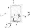
- FIG. 1 it is shown a NFC device 10, in particular in form of a NFC card, which operates as antifraud system according to the solution here described, indicated as a whole with the numerical reference 10.
- a NFC device 10 includes a plastic body 20, having a rectangular shape, which carries an integrated circuit 12, for instance the integrated circuit of a UICC card. Terminals 12a and 12b of the integrated circuit 12 are coupled to an antenna 14 obtained by a metal coil, in particular a track running along the periphery of the plastic body 20.
- the metal track of the antenna 14 starts in particular from the terminal 12a of the integrated circuit 12 and ends in the terminal 12b of the circuit 12, after performing several turns of the periphery of the body 20, in particular in the example three turns, so that, with the exception of where the tracks enter the terminals 12a, 12b, the antenna 14 defines three parallel metal coils co-planar with the plane of the body 20.
- the coils can be of course in a different number, depending on the parameters of the antenna 12.
- a current is generated in the coil of the antenna 14, this current can carry power supply to the integrated circuit 12 for operation.
- the NFC device 10 however includes also a photoresistive circuit, which is a arranged coupled on one of the coils of the antenna 14 and including a photo-resistance 13.
- the photoresistive circuit is configured to increase the resistance of the at least one antenna coil when the at least one photo-resistance is under dark conditions and thus is in its high resistance state.
- the photo-resistance 13 is arranged in series on the coil of the antenna 14, thus when in dark conditions, i.e. the photo-resistance is not reached by the light of a radiation source 16, which can be the sun or ambient lighting, the photo-resistance 13 has high value and increase the total resistance of the antenna 14, decreasing the value of the current generated under an operation threshold of the integrated circuit 12.
- the photo-resistance 13 When exposed to the light photo-resistance 13 has a lower value of resistance, increasing the value of the current generated over the operation threshold of the integrated circuit 12, which can in this way operate normally and can be read by the external reader.
- the photo-resistance 13 disables the electronic circuit 12 when it is not exposed to a light source, i.e. in dark conditions, and assure that no one is able to scan sensible data.
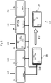
- FIG 2 it is shown a first schematic representation of the manufacturing process, indicated with the reference 100.
- the process includes providing 110 a first transparent plastic overlay sheet 21.
- the first overlay sheet 21 is a plastic transparent layer (PVC, PC, PET or other no conductive material) which operates as support of the structure determining the plastic body 20.
- the process further includes providing 120 a first cover sheet 22which is a preferably opaque plastic sheet, representing the rear side of the card 10.
- the process includes providing 130 a core layer 23, i.e. a layer, preferably a plastic layer, carrying the circuit components, i.e. the integrated circuit 12 connected to the coils of the antenna 14, and, in the example shown, the photo-resistance 13 connected in series on one of the coils for instance the most inner coil of the antenna 14.
- the processes for connecting such components on a plastic substrate are well known to the technicians in the field of Card and e-Passport Manufacturing. Then the process includes providing 140 140 a second cover sheet layer 24 carrying a window 24a, i.e. a hole punched or milled in the sheet 24, which, given a corresponding shape of the core sheet 23 and cover sheet 24, has substantially the same position and size of the photo-resistance 13.
- the second cover sheet layer 24 represents the front sheet of the card on which, for protection, a second transparent plastic sheet 25 is placed.
- a second cover sheet layer 24 carrying a hole 24a having the same position and size of the photo-resistance 13 is provided on the circuit sheet 13.
- the second cover sheet layer 24 represents the front sheet of the card 10: Then the process includes providing 150 a second transparent plastic sheet 2.5.
- All plastic sheets 21-25 in the example are rectangular with the same dimensions. In variant embodiments other shapes of the sheets 21-125 and the antenna 14 may be possible compatibly with the efficiency of the antenna 14. In variant embodiments one or more of the sheets 21-25 can be paper or cardboard sheets.
- the sheets 21-25 are stacked one upon the other, in that order, i.e. on the first transparent layer 21 is placed the first cover sheet 22, then on the first cover sheet 22 is placed the core sheet 23, the on the cover sheet 23 is placed the second cover sheet 23, so that the window 24a frames and contains the photo-resistance 13, finally the second transparent layer 25 is placed on the second cover sheet 24, covering the window 24a with an antiscratch protection which however allows the light reaching the photo-resistance 13 within the window 24a.
- the sheets are shown slightly horizontally shifted for better appreciating the order of the stack, however they have same dimensions and are vertically aligned (see lateral view of figure 3 ), so that when they are assembled together form a single card with the same dimension.
- FIG 3 the stack of figure 2 is shown in a lateral view.
- the sheets are vertically aligned, and the photo-resistance 13 is positioned on the core sheet 23 so that is aligned with the window 24a.
- a recess or, in the example shown, a window 13a obtained by a hole punched in the core sheet 23 is provided, so that the photo-resistance 13 is inserted within said window 13a.
- the body 20 is obtained and the window 13a and 24a are aligned containing the photo-resistance 13, where thickness of said cover sheet 24 summed to the thickness of the core sheet 23 is equal to the thickness, i.e. the vertical dimension, of the photo-resistance 13.
- the lower core sheet 22 can have a corresponding window for the case the photo-resistance has two photosensitive surfaces, upper and lower.
- the manufacturing process of the Near Field Communication device 10 includes basically providing the core sheet 23 carrying at least the integrated circuit 12 and at least one antenna coil 14, then arranging 160 the core sheet 23 within a stack 20aof plastic or paper sheets to form the card support body, laminating 170 said sheet stack 20a to obtain the support body 20, the process comprising also arranging at least a photo-resistance 13 coupled to one of the coils 14 and with at least a photosensitive surface facing outwards from an outer surface of the device support body 20.
- the process can include providing at least a core sheet 23 and a upper 22 and lower 24 cover sheet, the transparent sheets 21 and 25 being used as optional, although preferable, mechanical protection, making the passing window 24a in a vertically corresponding position at least in one of said upper and lower cover sheet 22, 24, and preferably a window 13a in said core sheet 23, arranging said photo-resistance 13 in the window 13a in the core sheet 23 if present or on the core sheet 23, stacking the core sheet 23 between said upper 22 and lower cover sheet 24 inserting the photo-resistance 13 in the window 24a in at least in one of said upper 22 and lower cover sheet to obtain the sheet stack 20a, in particular complete with sheets 21 and 25, laminating said sheet stack 20a to obtain said support body 20.
- this photoresistance may have an upper and a lower photosensitive surface.
- FIG 4 it is shown a variant embodiment of the manufacturing process of figure 3 , which includes providing punched transparent sheets 21, 25 as outer external sheets, and double photosensitive surface.
- a stack 30a includes the core sheet 23, positioned between the cover sheets 22, 24, which have a respective passing window 22a, 24a in correspondence of a photoresistance 13' arranged on the core sheet 23.
- the transparent sheets 21, 25 are placed as outer sheets under sheet 22 and over sheet 24 respectively, and are punched with passing windows 21a, 25a at the same position in the card plane of windows 22a, 24a.
- the photo-resistance 13' has an upper and a lower photosensitive surface, which can be reached from an upper light source 16 and lower light source 16'.
- the transparent overlay 21, 25 assures mechanical/functional performance, usually required for standard ID and financial applications, but does not assure an additional scratch resistance.
- the transparent sheets 21, 25 may not be punched, i.e. without windows 21a, 25a, for instance if the transparence of such sheets 21, 25 is such that it makes negligible the amount of illuminance subtracted from sheets 21,25 from the illuminance reaching the photoresistance 13 or 13'.
- the transparent sheets 21, 25 may be placed directly over the core sheet 23, with or without the windows 21a, 25a.
- the process includes providing at least a core sheet 23, stacking at least the core sheet between further layers, which forms the stack 40, laminating said sheet stack 40a to obtain said support body 40, then making a cavity 43a in the card support body 40 reaching said core sheet 23, in particular by a standard milling+embedding process, and arranging said photo-resistance 13 in said cavity 43a on said core sheet 23 electrically connected, by connections 13b, to the coil of antenna 14, in particular by physical soldering or using conductive glue.
- the variant embodiment of figure 5 describes a manufacturing process including providing 120 at least a core sheet 23, stacking 160 at least said core sheet 23 between further sheets, in particular the sheets 21, 22, 24, 25 like in figure 2 , laminating 170 the obtained sheet stack to obtain said support body 40, making a cavity 43a in the device support body 40 reaching said core sheet 23, in particular by a standard milling and embedding process, and arranging said photo-resistance 13 in the cavity 43a on said core sheet 23 electrically connected, by the connections 13b, to said at least one coil, in particular by physical soldering or using conductive glue.
- the variant embodiment of the manufacturing process described with reference to figure 6 includes providing a device support body 50 including a core sheet 23, which is in particular arranged near the surface, arranging said photo-resistance 13 on an outer surface of said support body (50) connected to said at least one coil 14, in particular by physical soldering or using conductive glue, in particular via through-holes in the upper transparent sheet 25.
- Figure 7 it is shown a diagram representing the qualitative characteristic curve of the photoresistance 13, in particular a resistance R13 of the photoresistance 13 as a function of the illuminance E.
- an exemplary value of threshold TH of the illuminance E is shown, having a value around 8 lux, corresponding to a 100 ⁇ resistance of the photoresist 13 which can correspond to dark conditions.
- Typical values of the supply current of a processor in the integrated circuit 12 are below 5 mA, therefore, the photoresistance 13 should be sized so that at the illuminance threshold TH the value of resistance R13 is that the current is below such limit of the supply current of the integrated circuit 12, in particular of its processor, e.g. is below 5 mA.
- the described solution thus provides removing a drawback of contactless solutions using NFC devices, exploiting the fact that while not in use, most NFC device, are in dark conditions, i.e. not reached by the light, thus their NFC device cannot be read until a positive action of exposing to the solar or ambient light is performed by the user. This allows to reject many attempts to fraud, by unauthorizedly reading the NFC device when not in use.
- the photoresistive circuit may include more than one photo-resistance or other light sensitive component, and can be arranged differently with respect to the coil, provided that the circuital arrangement of such photoresistive circuit is configured to increase the resistance of the at least one antenna coil when the at least one photo-resistance is in its high resistance state in dark conditions.
- the Near Field Communication device can be an UICC card or smartcard, or another type of NFC tag. Although most NFC devices are card with a parallelepiped card shape, the Near Field Communication device can have a different structure, like a fob or a keyring, or other structures used for contactless application using NFC.
Landscapes
- Engineering & Computer Science (AREA)
- Computer Hardware Design (AREA)
- Physics & Mathematics (AREA)
- Microelectronics & Electronic Packaging (AREA)
- General Physics & Mathematics (AREA)
- Theoretical Computer Science (AREA)
- Computer Networks & Wireless Communication (AREA)
- Signal Processing (AREA)
- Health & Medical Sciences (AREA)
- Toxicology (AREA)
- Artificial Intelligence (AREA)
- Computer Vision & Pattern Recognition (AREA)
- General Health & Medical Sciences (AREA)
- Electromagnetism (AREA)
- Computer Security & Cryptography (AREA)
- General Engineering & Computer Science (AREA)
- Credit Cards Or The Like (AREA)
- Electrotherapy Devices (AREA)
- Radar Systems Or Details Thereof (AREA)
- Control Of Motors That Do Not Use Commutators (AREA)
Abstract
Description
- Embodiments of the present disclosure relate to solutions of Near Field Communication (NFC) devices comprising a support body on which at least one antenna coil is arranged, on said support body being also arranged at least an integrated circuit connected to the at least one antenna coil.
- Embodiments of the present disclosure relate in particular to NFC devices like NFC plastic cards or tags and also to NFC devices including a body made at least in part of paper, like electronic passports, e-tickets.
- NFC (Near Field Communication) cards and tags are well known. Such NFC devices usually include a microchip or integrated circuit and an antenna comprising one or more coil, usually obtained by depositing metal tracks on a plane of the card. A NFC card reader, or initiator, is configured, in order to activate the operation of the integrated circuit, to generate a time variable magnetic field (e.g. at 13,56 MHz), which induces a current in the coil or coils of the antenna. Such electro-magnetically induced current is used for the power supply of the integrated circuit on the NFC device, which for instance performs the operation required and sends back through the same antenna the corresponding information to the reader.
- Such card are used for different application, like credit card, electronic passport and other contactless application, like access control and e-ticketing.
- A problem with this type of cards is that everyone who comes in a sufficiently proximity with the NFC device with a NFC reader, e.g. a smartphones routinely includes a NFC reader, can attempt a fraud using radiofrequency, i.e. attempt an unauthorized reading of the content of the NFC device with his NFC reader, scanning and copying its content, for instance the authentication content of a credit card or of a passport.
- Thus there is the need to offer a NFC device which is more secure and includes security and antifraud systems.
- On the basis of the foregoing description, the need is felt for solutions which overcome one or more of the previously outlined drawbacks.
- According to one or more embodiments, such an object is achieved through a Near Field Communication device having the features specifically set forth in the claims that follow. Embodiments moreover concerns a related NFC device manufacturing method.
- The claims are an integral part of the technical teaching of the disclosure provided herein.
- As mentioned in the foregoing, the present disclosure provides solutions regarding a Near Field Communication device comprising a support body on which at least one antenna coil is arranged, on said support body being also arranged at least an integrated circuit connected to the at least one antenna coil, characterized in that said near field communication device includes a photoresistive circuit arranged connected on said at least one antenna coil and including at least a photo-resistance, said photoresistive circuit being configured to increase the resistance of the at least one antenna coil when the at least one photo-resistance is in its high resistance state under dark conditions.
- In variant embodiments, the solution here described may include that the support body includes a core sheet carrying said integrated circuit and at least one antenna coil which includes a hole or a recess in which said photo-resistance is mounted.
- In variant embodiments, the solution here described may include that the support body includes a core sheet carrying said integrated circuit and at least one antenna coil, said core sheet being comprised between at least an upper and a lower sheet, said upper and/or lower sheet comprising a window in which said photo-resistance is mounted in said window.
- In variant embodiments, the solution here described may include that said photo-resistance includes an upper and lower photosensitive surface.
- In variant embodiments, the solution here described may include that said support body is substantially a planar body.
- In variant embodiments, the solution here described may include that said support body includes also transparent sheets forming its upper and/or lower outer surface.
- In variant embodiments, the solution here described may include that said core sheet has a passing hole and it is comprised between transparent sheets.
- In variant embodiments, the solution here described may include that said photo-resistance is arranged in a cavity in the support body reaching a core sheet carrying said integrated circuit and at least one antenna coil.
- In variant embodiments, the solution here described may include that said photo-resistance is arranged on an outer surface of said support body.
- In variant embodiments, the solution here described may include that one or more of said sheets are plastic sheets or paper sheets.
- The present disclosure provides also solutions regarding a process for manufacturing a Near Field Communication device as described above, comprising providing a core sheet carrying at least said integrated circuit and at least one antenna coil, arranging said core sheet within a stack of plastic or paper layers to form said card support body laminating said sheet stack to obtain said support body, said method comprising also arranging a photo-resistance electrically connected to said at least one coil and with at least a photosensitive surface facing outwards from an external surface of the card body.
- In variant embodiments, the process here described may include providing at least a core sheet and an at least an upper and lower cover sheet, making a window in a vertically corresponding position at least in one of said at least an upper and lower cover sheet and in said core sheet, arranging said photo-resistance in the window in the core sheet, stacking at least said core sheet between said upper and lower cover sheet to obtain a sheet stack laminating said sheet stack to obtain said support body.
- In variant embodiments, the process here described may include providing at least a core sheet, making a window in said core sheet, arranging said photo-resistance in the window in the core sheet, said photo-resistance including an upper and lower photosensitive surface.
- Stacking at least said core sheet in a stack comprising a transparent upper and lower overlay sheet to obtain a sheet stack, laminating said sheet stack to obtain said support body.
- In variant embodiments, the process here described may include stacking at least said core sheet in a stack comprising providing also an upper and lower cover sheet between the transparent upper and lower overlay sheet, making a window in a vertically corresponding position to the window in said core sheet at least in said upper and lower cover sheet.
- In variant embodiments, the process here described may include providing at least a core sheet, stacking at least said core sheet between further layers laminating said sheet stack to obtain said support body, making a cavity in the card support body reaching said core sheet, in particular by a standard milling+embedding process, and arranging said photo-resistance in said cavity on said core sheet electrically connected to said at least one coil, in particular by physical soldering or using conductive glue.
- In variant embodiments, the process here described may include providing a card support body including a core sheet arranging said photo-resistance on an external surface of said support body connected to said at least one coil, in particular by physical soldering or using conductive glue.
- In variant embodiments, the process here described may include that the thickness of said cover sheet or of both the cover sheets summed to the thickness of the core sheet is equal to the thickness of the photo-resistance.
- In variant embodiments, the process here described may include placing on the outer surfaces of the stack a scratch resistant transparent overlay sheet.
- Embodiments of the present disclosure will now be described with reference to the annexed drawings, which are provided purely by way of non-limiting example and in which:
-
Figure 1 shows schematically a Near Field Communication device according to the solution here described; -
Figure 2 shows schematically in plan view components and operation of an embodiment of a manufacturing process of the Near Field Communication device here described; -
Figure 3 shows schematically in lateral view components and operation of the embodiment of a manufacturing process of the Near Field Communication device here described; -
Figure 4 shows schematically in lateral view components and operation of a second embodiment of a manufacturing process of the Near Field Communication device here described; -
Figure 5 shows schematically in lateral view components and operation of a third embodiment of a manufacturing process of the Near Field Communication device here described; -
Figure 6 shows schematically in lateral view components and operation of a fourth embodiment of a manufacturing process of the Near Field Communication device here described; -
Figure 7 shows a diagram representing a qualitative characteristic curve of a photoresistance which may be used in the Near Field Communication device here described. - In the following description, numerous specific details are given to provide a thorough understanding of embodiments. The embodiments can be practiced without one or several specific details, or with other methods, components, materials, etc. In other instances, well-known structures, materials, or operations are not shown or described in detail to avoid obscuring aspects of the embodiments.
- Reference throughout this specification to "one embodiment" or "an embodiment" means that a particular feature, structure, or characteristic described in connection with the embodiment is included in at least one embodiment. Thus, the appearances of the phrases "in one embodiment" or "in an embodiment" in various places throughout this specification are not necessarily all referring to the same embodiment. Furthermore, the particular features, structures, or characteristics may be combined in any suitable manner in one or more embodiments.
- The headings provided herein are for convenience only and do not interpret the scope or meaning of the embodiments.
- Figures parts, elements or components which have already been described with reference to
Figures 1 to 5 are denoted by the same references previously used in such Figures; the description of such previously described elements will not be repeated in the following in order not to overburden the present detailed description. - The solution here described in particular regards a near field communication device which includes a photoresistive circuit arranged connected on said at least one antenna coil and including at least a photo-resistance, said photoresistive circuit being configured to increase the resistance of the at least one antenna coil when the at least one photo-resistance is under dark conditions.
- The value of the resistance increase, in particular of the photo-resistance, is calculated so that when a NFC reader sends an alternate magnetic field, the current generated in the
coil 14 in dark conditions, i.e. a dark current, is under a current threshold sufficient to activate the integrated circuit. - In this way, when the
NFC device 10 is in dark conditions it is disabled, ie its integrated circuit is not operating and an unauthorized access to the NFC device cannot succeed. Dark conditions are defined by an amount of light level coming from the sun or from an illumination source below a certain threshold that put the photo-resistance 13, in a high resistance state, as opposed to a low resistance state when it is illuminated by light of an amount above a certain threshold. - Since while not in use, most NFC device, like credit cards or e-ticket kept in wallet and folded electronic passports, are in dark conditions, their NFC device cannot be read until a positive action of exposing to the solar or ambient light is performed by the user.
- To this regard, in
figure 1 it is shown aNFC device 10, in particular in form of a NFC card, which operates as antifraud system according to the solution here described, indicated as a whole with thenumerical reference 10.Such card 10 includes aplastic body 20, having a rectangular shape, which carries anintegrated circuit 12, for instance the integrated circuit of a UICC card.Terminals circuit 12 are coupled to anantenna 14 obtained by a metal coil, in particular a track running along the periphery of theplastic body 20. The metal track of theantenna 14 starts in particular from theterminal 12a of theintegrated circuit 12 and ends in theterminal 12b of thecircuit 12, after performing several turns of the periphery of thebody 20, in particular in the example three turns, so that, with the exception of where the tracks enter theterminals antenna 14 defines three parallel metal coils co-planar with the plane of thebody 20. The coils can be of course in a different number, depending on the parameters of theantenna 12. As known to the person skilled in the art, when a varying magnetic field is generated by a reader, a current is generated in the coil of theantenna 14, this current can carry power supply to the integratedcircuit 12 for operation. - The
NFC device 10 however includes also a photoresistive circuit, which is a arranged coupled on one of the coils of theantenna 14 and including a photo-resistance 13. The photoresistive circuit is configured to increase the resistance of the at least one antenna coil when the at least one photo-resistance is under dark conditions and thus is in its high resistance state. To this purpose in the example the photo-resistance 13 is arranged in series on the coil of theantenna 14, thus when in dark conditions, i.e. the photo-resistance is not reached by the light of aradiation source 16, which can be the sun or ambient lighting, the photo-resistance 13 has high value and increase the total resistance of theantenna 14, decreasing the value of the current generated under an operation threshold of theintegrated circuit 12. When exposed to the light photo-resistance 13 has a lower value of resistance, increasing the value of the current generated over the operation threshold of theintegrated circuit 12, which can in this way operate normally and can be read by the external reader. - Thus, the photo-
resistance 13 disables theelectronic circuit 12 when it is not exposed to a light source, i.e. in dark conditions, and assure that no one is able to scan sensible data. - With reference to
figure 2 is described a manufacturing process of thecard 10, which adds a photo-resist 13 in series with theantenna 14 inside a plastic or paper body, like the one used in credit cards, badge, e-ticket, holder page of a passport. - In
figure 2 it is shown a first schematic representation of the manufacturing process, indicated with thereference 100. The process includes providing 110 a first transparentplastic overlay sheet 21. Thefirst overlay sheet 21 is a plastic transparent layer (PVC, PC, PET or other no conductive material) which operates as support of the structure determining theplastic body 20. The process further includes providing 120 a first cover sheet 22which is a preferably opaque plastic sheet, representing the rear side of thecard 10. Then the process includes providing 130 acore layer 23, i.e. a layer, preferably a plastic layer, carrying the circuit components, i.e. theintegrated circuit 12 connected to the coils of theantenna 14, and, in the example shown, the photo-resistance 13 connected in series on one of the coils for instance the most inner coil of theantenna 14. The processes for connecting such components on a plastic substrate are well known to the technicians in the field of Card and e-Passport Manufacturing. Then the process includes providing 140 140 a secondcover sheet layer 24 carrying awindow 24a, i.e. a hole punched or milled in thesheet 24, which, given a corresponding shape of thecore sheet 23 andcover sheet 24, has substantially the same position and size of the photo-resistance 13. The secondcover sheet layer 24 represents the front sheet of the card on which, for protection, a secondtransparent plastic sheet 25 is placed. - In a step 140 a second
cover sheet layer 24 carrying ahole 24a having the same position and size of the photo-resistance 13 is provided on thecircuit sheet 13. The secondcover sheet layer 24 represents the front sheet of the card 10: Then the process includes providing 150 a second transparent plastic sheet 2.5. - All plastic sheets 21-25 in the example are rectangular with the same dimensions. In variant embodiments other shapes of the sheets 21-125 and the
antenna 14 may be possible compatibly with the efficiency of theantenna 14. In variant embodiments one or more of the sheets 21-25 can be paper or cardboard sheets. - Then in a
coupling operation 160 the sheets 21-25 are stacked one upon the other, in that order, i.e. on the firsttransparent layer 21 is placed thefirst cover sheet 22, then on thefirst cover sheet 22 is placed thecore sheet 23, the on thecover sheet 23 is placed thesecond cover sheet 23, so that thewindow 24a frames and contains the photo-resistance 13, finally the secondtransparent layer 25 is placed on thesecond cover sheet 24, covering thewindow 24a with an antiscratch protection which however allows the light reaching the photo-resistance 13 within thewindow 24a. Infigure 2 the sheets are shown slightly horizontally shifted for better appreciating the order of the stack, however they have same dimensions and are vertically aligned (see lateral view offigure 3 ), so that when they are assembled together form a single card with the same dimension. - To assemble together the stack of sheets 21-25 is then performed a
lamination process 170 to obtain theplastic body 20 of thecard 10. - In
figure 3 the stack offigure 2 is shown in a lateral view. As it can be seen the sheets are vertically aligned, and the photo-resistance 13 is positioned on thecore sheet 23 so that is aligned with thewindow 24a. In particular at the position of thewindow 24a, a recess or, in the example shown, awindow 13a obtained by a hole punched in thecore sheet 23 is provided, so that the photo-resistance 13 is inserted within saidwindow 13a. After thecoupling 160 and lamination, as shown infigure 3 , thebody 20 is obtained and thewindow resistance 13, where thickness of saidcover sheet 24 summed to the thickness of thecore sheet 23 is equal to the thickness, i.e. the vertical dimension, of the photo-resistance 13. In variant embodiments also thelower core sheet 22 can have a corresponding window for the case the photo-resistance has two photosensitive surfaces, upper and lower. - Thus, with reference to
figures 2 and3 , in general the manufacturing process of the NearField Communication device 10 includes basically providing thecore sheet 23 carrying at least theintegrated circuit 12 and at least oneantenna coil 14, then arranging 160 thecore sheet 23 within a stack 20aof plastic or paper sheets to form the card support body, laminating 170 saidsheet stack 20a to obtain thesupport body 20, the process comprising also arranging at least a photo-resistance 13 coupled to one of thecoils 14 and with at least a photosensitive surface facing outwards from an outer surface of thedevice support body 20. - Also in variant embodiments the process can include providing at least a
core sheet 23 and a upper 22 and lower 24 cover sheet, thetransparent sheets window 24a in a vertically corresponding position at least in one of said upper andlower cover sheet window 13a in saidcore sheet 23, arranging said photo-resistance 13 in thewindow 13a in thecore sheet 23 if present or on thecore sheet 23, stacking thecore sheet 23 between said upper 22 andlower cover sheet 24 inserting the photo-resistance 13 in thewindow 24a in at least in one of said upper 22 and lower cover sheet to obtain thesheet stack 20a, in particular complete withsheets sheet stack 20a to obtain saidsupport body 20. - If both cover
sheets resistance 13, this photoresistance may have an upper and a lower photosensitive surface. - In
figure 4 it is shown a variant embodiment of the manufacturing process offigure 3 , which includes providing punchedtransparent sheets core sheet 23, positioned between thecover sheets window core sheet 23. Thetransparent sheets sheet 22 and oversheet 24 respectively, and are punched with passingwindows windows light source 16 and lower light source 16'. As mentioned thetransparent overlay transparent sheets windows such sheets sheets photoresistance 13 or 13'. In further variant embodiments thetransparent sheets core sheet 23, with or without thewindows - Thus in this variant embodiment it is provided stacking the
core sheet 23 between a transparent upper andlower overlay sheet - As shown in
figure 5 , it is possible to use a standard milling and embedding process to make a cavity on thecard body 20 to hold the photo-resistance 13. The connection with theantenna 14 it ispossible trough connections 13b obtained physical soldering or using conductive glue. Thus in this case the process includes providing at least acore sheet 23, stacking at least the core sheet between further layers, which forms thestack 40, laminating said sheet stack 40a to obtain saidsupport body 40, then making acavity 43a in thecard support body 40 reaching saidcore sheet 23, in particular by a standard milling+embedding process, and arranging said photo-resistance 13 in saidcavity 43a on saidcore sheet 23 electrically connected, byconnections 13b, to the coil ofantenna 14, in particular by physical soldering or using conductive glue. Thus the variant embodiment offigure 5 describes a manufacturing process including providing 120 at least acore sheet 23, stacking 160 at least saidcore sheet 23 between further sheets, in particular thesheets figure 2 , laminating 170 the obtained sheet stack to obtain saidsupport body 40, making acavity 43a in thedevice support body 40 reaching saidcore sheet 23, in particular by a standard milling and embedding process, and arranging said photo-resistance 13 in thecavity 43a on saidcore sheet 23 electrically connected, by theconnections 13b, to said at least one coil, in particular by physical soldering or using conductive glue. - Also as shown in
figure 6 it is possible to lay the photo-resistance 13 on one of the external faces of the card, 10, i.e. ofe a body 50.Connections 13b with theantenna 14 it is possible through physical soldering or using conductive glue. This variant of the process is in particular for structure not made with plastic materials, in particular body containing paper sheets, such as (e-ticket, passport with holder page in paper. - Thus in this the case the variant embodiment of the manufacturing process described with reference to
figure 6 includes providing adevice support body 50 including acore sheet 23, which is in particular arranged near the surface, arranging said photo-resistance 13 on an outer surface of said support body (50) connected to said at least onecoil 14, in particular by physical soldering or using conductive glue, in particular via through-holes in the uppertransparent sheet 25. -
Figure 7 it is shown a diagram representing the qualitative characteristic curve of thephotoresistance 13, in particular a resistance R13 of thephotoresistance 13 as a function of the illuminance E. Infigure 7 it is shown also an exemplary value of threshold TH of the illuminance E is shown, having a value around 8 lux, corresponding to a 100Ω resistance of thephotoresist 13 which can correspond to dark conditions. Typical values of the supply current of a processor in theintegrated circuit 12 are below 5 mA, therefore, thephotoresistance 13 should be sized so that at the illuminance threshold TH the value of resistance R13 is that the current is below such limit of the supply current of theintegrated circuit 12, in particular of its processor, e.g. is below 5 mA. - The described solution thus provides removing a drawback of contactless solutions using NFC devices, exploiting the fact that while not in use, most NFC device, are in dark conditions, i.e. not reached by the light, thus their NFC device cannot be read until a positive action of exposing to the solar or ambient light is performed by the user. This allows to reject many attempts to fraud, by unauthorizedly reading the NFC device when not in use.
- Of course, without prejudice to the principle of the invention, the details of construction and the embodiments may vary widely with respect to what has been described and illustrated herein purely by way of example, without thereby departing from the scope of the present invention, as defined by the ensuing claims.
- In variant embodiments, the photoresistive circuit may include more than one photo-resistance or other light sensitive component, and can be arranged differently with respect to the coil, provided that the circuital arrangement of such photoresistive circuit is configured to increase the resistance of the at least one antenna coil when the at least one photo-resistance is in its high resistance state in dark conditions.
- As mentioned the Near Field Communication device can be an UICC card or smartcard, or another type of NFC tag. Although most NFC devices are card with a parallelepiped card shape, the Near Field Communication device can have a different structure, like a fob or a keyring, or other structures used for contactless application using NFC.
Claims (18)
- Near Field Communication device comprising a device support body (20; 30; 40; 50) on which at least one antenna coil (14) is arranged, on said support body (20; 30; 40; 50) being also arranged at least an integrated circuit (12) coupled to the at least one antenna coil (14), characterized in that said Near Field Communication device (10) includes a photoresistive circuit arranged coupled to said at least one antenna coil (14) and including at least a photo-resistance (13), said photoresistive circuit being configured to increase the resistance of the at least one antenna coil (14) when the at least one photo-resistance (13) is in its high resistance state in dark conditions.
- The device of claim 1, characterized in that the support body (20; 30; 40; 50) includes a core sheet (23) carrying said integrated circuit (12) and the at least one antenna coil (14) which includes a hole or a recess (13a) in which said photo-resistance (13) is mounted.
- The device of claim 1 or 2, characterized in that_the support body (20; 30; 40; 50) includes a core sheet (23) carrying said integrated circuit (12) and the at least one antenna coil (14), said core sheet (23) being comprised between at least an upper (22) and a lower sheet (24), said upper and/or lower sheet comprising a window (24a) in which said photo-resistance (13) is mounted in said window (24a).
- The device of any of claims 1 to 3, characterized in that said photo-resistance (13) includes an upper and lower photosensitive surface.
- The device of any of the previous claims, characterized in that said support body (20; 30; 40; 50) is substantially a planar body.
- The device of any of the previous claims, characterized in that said support body (20; 30; 40; 50) includes transparent sheets (21, 25) forming its upper and/or lower outer surface.
- The device of any of the previous claims, characterized in that said core sheet (23) has a passing hole (13a) and it is comprised between transparent sheets (21, 25).
- The device of claim 1, characterized in that said photo-resistance (13) is arranged in a cavity in the support body reaching a core sheet (23) carrying said integrated circuit (12) and the at least one antenna coil (14).
- The device of claim 1, characterized in that said photo-resistance (13) is arranged on an outer surface of said support body (50).
- The device of any of the previous claims, characterized in that one or more of said sheets (21, 22, 23, 34, 25) are plastic sheets or paper sheets.
- Manufacturing process of a near field communication device according to any of claims 1 to 10, comprising providing a core sheet (23) carrying at least said integrated circuit (12) and the at least one antenna coil (14), arranging said core sheet (23) within a stack (20a; 30a; 40a; 50a) of plastic or paper sheets to form said card support body (20; 30; 40; 50), laminating said sheet stack (20a; 30a; 40a; 50a) to obtain said support body (20; 30; 40; 50), said process comprising also arranging at least a photo-resistance (13) electrically connected to said at least one coil (14) and with at least a photosensitive surface facing outwards from an outer surface of the device support body (20; 30; 40; 50).
- The process of claim 11, including providing (120, 130, 140) at least a core sheet (23) and a upper (22) and lower (24) cover sheet, making a window in a vertically corresponding position at least in one of said upper (22) and lower cover sheet (24) and a window (13a) in said core sheet (23), arranging said photo-resistance (13) in the window (13a) in the core sheet (23), stacking (160) at least said core sheet (23) between said upper (22) and lower cover sheet (24) inserting said photo-resistance (13) in the window (24a) at least in one of said upper (22) and lower cover sheet to obtain a sheet stack (20a) laminating said sheet stack (20a) to obtain said support body (20) .
- The process of claim 11, including providing (120) at least a core sheet (23), making a window (13a) in said core sheet (23), arranging said photo-resistance (13') in the window (13a) in the core sheet, said photo-resistance (13') including an upper and lower photosensitive surface.
Stacking (160) at least said core sheet in a stack (30a) comprising a transparent upper and lower overlay sheet (21, 25) to obtain a sheet stack (30a), laminating (170) said sheet stack (30a) to obtain said support body (30). - The process of claim 13, wherein said stacking (160) at least said core sheet in a stack (30a) comprises providing also an upper (22) and lower (24) cover sheet between said transparent upper and lower overlay sheet (21, 25), making a window in a vertically corresponding position to the window (13a) in said core sheet (23) at least in said upper (22) and lower cover sheet (24).
- The process of claim 11, including providing (120) at least a core sheet (23), stacking (160) at least said core sheet (23) between further sheets, laminating (170) said sheet stack (40a) to obtain said support body (40), making a cavity in the device support body (40) reaching said core sheet (23), in particular by a standard milling and embedding process, and arranging said photo-resistance in said cavity on said core sheet electrically connected to said at least one coil, in particular by physical soldering or using conductive glue.
- The process of claim 11, including providing a device support body (50) including a core sheet (23), arranging said photo-resistance (13) on an outer surface of said support body (50) connected to said at least one coil (14), in particular by physical soldering or using conductive glue.
- The process of any of the previous claims from 11 to 15, wherein the thickness of said cover sheet (24) or of both the cover sheets (22, 24) summed to the thickness of the core sheet (23) is equal to the thickness of the photo-resistance.
- The process of any of the previous claims from 11 to 17, wherein includes placing on the outer surfaces of the stack (20a, 30a) a scratch resistant transparent overlay sheet (21, 25).
Applications Claiming Priority (1)
| Application Number | Priority Date | Filing Date | Title |
|---|---|---|---|
| IT102018000004051A IT201800004051A1 (en) | 2018-03-28 | 2018-03-28 | NEAR FIELD COMMUNICATION DEVICE AND CORRESPONDING MANUFACTURING PROCEDURE |
Publications (2)
| Publication Number | Publication Date |
|---|---|
| EP3547726A1 true EP3547726A1 (en) | 2019-10-02 |
| EP3547726B1 EP3547726B1 (en) | 2022-05-04 |
Family
ID=62530509
Family Applications (1)
| Application Number | Title | Priority Date | Filing Date |
|---|---|---|---|
| EP19163247.0A Active EP3547726B1 (en) | 2018-03-28 | 2019-03-15 | Near field communication device and corresponding manufacturing process |
Country Status (4)
| Country | Link |
|---|---|
| US (1) | US11003973B2 (en) |
| EP (1) | EP3547726B1 (en) |
| CN (2) | CN209625254U (en) |
| IT (1) | IT201800004051A1 (en) |
Cited By (1)
| Publication number | Priority date | Publication date | Assignee | Title |
|---|---|---|---|---|
| FR3132581A1 (en) * | 2022-02-09 | 2023-08-11 | Stmicroelectronics (Rousset) Sas | Contactless communication device |
Families Citing this family (3)
| Publication number | Priority date | Publication date | Assignee | Title |
|---|---|---|---|---|
| IT201800004051A1 (en) * | 2018-03-28 | 2019-09-28 | St Microelectronics Srl | NEAR FIELD COMMUNICATION DEVICE AND CORRESPONDING MANUFACTURING PROCEDURE |
| US10885514B1 (en) * | 2019-07-15 | 2021-01-05 | Capital One Services, Llc | System and method for using image data to trigger contactless card transactions |
| EP4498283A1 (en) * | 2023-07-24 | 2025-01-29 | HID Global CID SAS | Identification document with activatable security feature |
Citations (2)
| Publication number | Priority date | Publication date | Assignee | Title |
|---|---|---|---|---|
| CN102663472A (en) * | 2012-04-17 | 2012-09-12 | 姚学民 | Contactless radio frequency card capable of preventing unauthorized swiping |
| US20150044966A1 (en) * | 2012-03-28 | 2015-02-12 | Xped Holdings Pty Ltd | Method and apparatus for forming associations and communicating between devices |
Family Cites Families (11)
| Publication number | Priority date | Publication date | Assignee | Title |
|---|---|---|---|---|
| US3664244A (en) * | 1970-09-10 | 1972-05-23 | Eastman Kodak Co | Indicating apparatus for exposure control apparatus |
| DE102005039319A1 (en) * | 2005-08-19 | 2007-02-22 | Giesecke & Devrient Gmbh | Card-shaped data carrier |
| US20070040683A1 (en) * | 2005-08-22 | 2007-02-22 | Neal Oliver | Light-activated RFID tag |
| US20080061149A1 (en) * | 2006-09-11 | 2008-03-13 | Colin Tanner | Proximity payment card with security interlock |
| US7561047B2 (en) * | 2006-11-22 | 2009-07-14 | Dai Nippon Printing Co., Ltd. | Noncontact tag and method for producing the same |
| US20120248201A1 (en) * | 2011-01-31 | 2012-10-04 | American Bank Note Company | Dual-interface smart card |
| US9208424B2 (en) * | 2013-10-06 | 2015-12-08 | Tyfone, Inc. | Active control secure transaction card |
| US9483723B2 (en) * | 2013-10-06 | 2016-11-01 | Tyfone, Inc. | Passive control secure transaction card |
| GB2525869A (en) * | 2014-05-06 | 2015-11-11 | Johnson Electric Sa | Smart card module |
| WO2017066462A1 (en) * | 2015-10-14 | 2017-04-20 | Capital One Services, Llc | Multilayer composite backed card |
| IT201800004051A1 (en) * | 2018-03-28 | 2019-09-28 | St Microelectronics Srl | NEAR FIELD COMMUNICATION DEVICE AND CORRESPONDING MANUFACTURING PROCEDURE |
-
2018
- 2018-03-28 IT IT102018000004051A patent/IT201800004051A1/en unknown
-
2019
- 2019-03-15 EP EP19163247.0A patent/EP3547726B1/en active Active
- 2019-03-27 CN CN201920401181.7U patent/CN209625254U/en active Active
- 2019-03-27 CN CN201910239978.6A patent/CN110321990B/en active Active
- 2019-03-28 US US16/368,162 patent/US11003973B2/en active Active
Patent Citations (2)
| Publication number | Priority date | Publication date | Assignee | Title |
|---|---|---|---|---|
| US20150044966A1 (en) * | 2012-03-28 | 2015-02-12 | Xped Holdings Pty Ltd | Method and apparatus for forming associations and communicating between devices |
| CN102663472A (en) * | 2012-04-17 | 2012-09-12 | 姚学民 | Contactless radio frequency card capable of preventing unauthorized swiping |
Cited By (2)
| Publication number | Priority date | Publication date | Assignee | Title |
|---|---|---|---|---|
| FR3132581A1 (en) * | 2022-02-09 | 2023-08-11 | Stmicroelectronics (Rousset) Sas | Contactless communication device |
| US12079679B2 (en) | 2022-02-09 | 2024-09-03 | Stmicroelectronics (Rousset) Sas | Contactless communication device |
Also Published As
| Publication number | Publication date |
|---|---|
| IT201800004051A1 (en) | 2019-09-28 |
| US20190303736A1 (en) | 2019-10-03 |
| US11003973B2 (en) | 2021-05-11 |
| CN110321990A (en) | 2019-10-11 |
| CN110321990B (en) | 2023-08-01 |
| EP3547726B1 (en) | 2022-05-04 |
| CN209625254U (en) | 2019-11-12 |
Similar Documents
| Publication | Publication Date | Title |
|---|---|---|
| EP3547726B1 (en) | Near field communication device and corresponding manufacturing process | |
| RU2470370C1 (en) | Element having at least two microelectronic non-contact data communication devices | |
| US20240121299A1 (en) | Systems and methods for constructing programmable credential and security cards | |
| US11847518B2 (en) | Systems and methods for constructing programmable credential and security cards | |
| JP5175747B2 (en) | Documents and information input methods such as valuable documents or security documents | |
| EP3723994B1 (en) | Improved illuminable card | |
| US20250390696A1 (en) | Illuminating transaction card | |
| ES2439942T3 (en) | Secure document, especially electronic passport with enhanced security | |
| CA2489152A1 (en) | Wallet card with built-in light | |
| US20080001844A1 (en) | Masking device for contactless portable object in the form of a secure document equipped with a radiofrequency device | |
| JP2006519714A (en) | Book cover insert and book type security document, and book cover insert and book type security document manufacturing method | |
| CN103268512A (en) | Mobile phone protection shell and method for integrating anti-electromagnetic interference smart card in mobile phone protection shell | |
| WO2018105495A1 (en) | Hinged laminate body, booklet, and laminate body | |
| JP2024520698A5 (en) | ||
| EP4719780A1 (en) | A pre-laminated structure with a see-through window and a method of forming it | |
| CN215008553U (en) | NFC antenna structure, screen assembly and terminal equipment | |
| RU215746U1 (en) | Payment smart card with dual interface and LEDs | |
| CN113661500A (en) | Switch button for contactless passive NFC and RFID devices | |
| CN209879558U (en) | Intelligent card with photosensitive sensor | |
| RU2831929C2 (en) | Contactless smart card in form of sticker | |
| EP1724711A1 (en) | A positioning system for keeping an electronic document on a contactless reader antenna | |
| KR200335758Y1 (en) | Luminous Plastic Card | |
| RU82052U1 (en) | PLASTIC CARRIER OF THE CONTACTLESS TYPE FOR ACCESS TO INFORMATION SYSTEMS | |
| KR20120077847A (en) | Coated film and security system having printing type rfid | |
| US7000843B2 (en) | Luminescent card device |
Legal Events
| Date | Code | Title | Description |
|---|---|---|---|
| PUAI | Public reference made under article 153(3) epc to a published international application that has entered the european phase |
Free format text: ORIGINAL CODE: 0009012 |
|
| STAA | Information on the status of an ep patent application or granted ep patent |
Free format text: STATUS: THE APPLICATION HAS BEEN PUBLISHED |
|
| AK | Designated contracting states |
Kind code of ref document: A1 Designated state(s): AL AT BE BG CH CY CZ DE DK EE ES FI FR GB GR HR HU IE IS IT LI LT LU LV MC MK MT NL NO PL PT RO RS SE SI SK SM TR |
|
| AX | Request for extension of the european patent |
Extension state: BA ME |
|
| STAA | Information on the status of an ep patent application or granted ep patent |
Free format text: STATUS: REQUEST FOR EXAMINATION WAS MADE |
|
| 17P | Request for examination filed |
Effective date: 20200319 |
|
| RBV | Designated contracting states (corrected) |
Designated state(s): AL AT BE BG CH CY CZ DE DK EE ES FI FR GB GR HR HU IE IS IT LI LT LU LV MC MK MT NL NO PL PT RO RS SE SI SK SM TR |
|
| STAA | Information on the status of an ep patent application or granted ep patent |
Free format text: STATUS: EXAMINATION IS IN PROGRESS |
|
| 17Q | First examination report despatched |
Effective date: 20200710 |
|
| GRAP | Despatch of communication of intention to grant a patent |
Free format text: ORIGINAL CODE: EPIDOSNIGR1 |
|
| STAA | Information on the status of an ep patent application or granted ep patent |
Free format text: STATUS: GRANT OF PATENT IS INTENDED |
|
| INTG | Intention to grant announced |
Effective date: 20211122 |
|
| GRAS | Grant fee paid |
Free format text: ORIGINAL CODE: EPIDOSNIGR3 |
|
| GRAA | (expected) grant |
Free format text: ORIGINAL CODE: 0009210 |
|
| STAA | Information on the status of an ep patent application or granted ep patent |
Free format text: STATUS: THE PATENT HAS BEEN GRANTED |
|
| AK | Designated contracting states |
Kind code of ref document: B1 Designated state(s): AL AT BE BG CH CY CZ DE DK EE ES FI FR GB GR HR HU IE IS IT LI LT LU LV MC MK MT NL NO PL PT RO RS SE SI SK SM TR |
|
| REG | Reference to a national code |
Ref country code: GB Ref legal event code: FG4D |
|
| REG | Reference to a national code |
Ref country code: CH Ref legal event code: EP |
|
| REG | Reference to a national code |
Ref country code: AT Ref legal event code: REF Ref document number: 1490442 Country of ref document: AT Kind code of ref document: T Effective date: 20220515 |
|
| REG | Reference to a national code |
Ref country code: DE Ref legal event code: R096 Ref document number: 602019014320 Country of ref document: DE |
|
| REG | Reference to a national code |
Ref country code: IE Ref legal event code: FG4D |
|
| REG | Reference to a national code |
Ref country code: LT Ref legal event code: MG9D |
|
| REG | Reference to a national code |
Ref country code: NL Ref legal event code: MP Effective date: 20220504 |
|
| REG | Reference to a national code |
Ref country code: AT Ref legal event code: MK05 Ref document number: 1490442 Country of ref document: AT Kind code of ref document: T Effective date: 20220504 |
|
| PG25 | Lapsed in a contracting state [announced via postgrant information from national office to epo] |
Ref country code: SE Free format text: LAPSE BECAUSE OF FAILURE TO SUBMIT A TRANSLATION OF THE DESCRIPTION OR TO PAY THE FEE WITHIN THE PRESCRIBED TIME-LIMIT Effective date: 20220504 Ref country code: PT Free format text: LAPSE BECAUSE OF FAILURE TO SUBMIT A TRANSLATION OF THE DESCRIPTION OR TO PAY THE FEE WITHIN THE PRESCRIBED TIME-LIMIT Effective date: 20220905 Ref country code: NO Free format text: LAPSE BECAUSE OF FAILURE TO SUBMIT A TRANSLATION OF THE DESCRIPTION OR TO PAY THE FEE WITHIN THE PRESCRIBED TIME-LIMIT Effective date: 20220804 Ref country code: NL Free format text: LAPSE BECAUSE OF FAILURE TO SUBMIT A TRANSLATION OF THE DESCRIPTION OR TO PAY THE FEE WITHIN THE PRESCRIBED TIME-LIMIT Effective date: 20220504 Ref country code: LT Free format text: LAPSE BECAUSE OF FAILURE TO SUBMIT A TRANSLATION OF THE DESCRIPTION OR TO PAY THE FEE WITHIN THE PRESCRIBED TIME-LIMIT Effective date: 20220504 Ref country code: HR Free format text: LAPSE BECAUSE OF FAILURE TO SUBMIT A TRANSLATION OF THE DESCRIPTION OR TO PAY THE FEE WITHIN THE PRESCRIBED TIME-LIMIT Effective date: 20220504 Ref country code: GR Free format text: LAPSE BECAUSE OF FAILURE TO SUBMIT A TRANSLATION OF THE DESCRIPTION OR TO PAY THE FEE WITHIN THE PRESCRIBED TIME-LIMIT Effective date: 20220805 Ref country code: FI Free format text: LAPSE BECAUSE OF FAILURE TO SUBMIT A TRANSLATION OF THE DESCRIPTION OR TO PAY THE FEE WITHIN THE PRESCRIBED TIME-LIMIT Effective date: 20220504 Ref country code: ES Free format text: LAPSE BECAUSE OF FAILURE TO SUBMIT A TRANSLATION OF THE DESCRIPTION OR TO PAY THE FEE WITHIN THE PRESCRIBED TIME-LIMIT Effective date: 20220504 Ref country code: BG Free format text: LAPSE BECAUSE OF FAILURE TO SUBMIT A TRANSLATION OF THE DESCRIPTION OR TO PAY THE FEE WITHIN THE PRESCRIBED TIME-LIMIT Effective date: 20220804 Ref country code: AT Free format text: LAPSE BECAUSE OF FAILURE TO SUBMIT A TRANSLATION OF THE DESCRIPTION OR TO PAY THE FEE WITHIN THE PRESCRIBED TIME-LIMIT Effective date: 20220504 |
|
| PG25 | Lapsed in a contracting state [announced via postgrant information from national office to epo] |
Ref country code: RS Free format text: LAPSE BECAUSE OF FAILURE TO SUBMIT A TRANSLATION OF THE DESCRIPTION OR TO PAY THE FEE WITHIN THE PRESCRIBED TIME-LIMIT Effective date: 20220504 Ref country code: PL Free format text: LAPSE BECAUSE OF FAILURE TO SUBMIT A TRANSLATION OF THE DESCRIPTION OR TO PAY THE FEE WITHIN THE PRESCRIBED TIME-LIMIT Effective date: 20220504 Ref country code: LV Free format text: LAPSE BECAUSE OF FAILURE TO SUBMIT A TRANSLATION OF THE DESCRIPTION OR TO PAY THE FEE WITHIN THE PRESCRIBED TIME-LIMIT Effective date: 20220504 Ref country code: IS Free format text: LAPSE BECAUSE OF FAILURE TO SUBMIT A TRANSLATION OF THE DESCRIPTION OR TO PAY THE FEE WITHIN THE PRESCRIBED TIME-LIMIT Effective date: 20220904 |
|
| PG25 | Lapsed in a contracting state [announced via postgrant information from national office to epo] |
Ref country code: SM Free format text: LAPSE BECAUSE OF FAILURE TO SUBMIT A TRANSLATION OF THE DESCRIPTION OR TO PAY THE FEE WITHIN THE PRESCRIBED TIME-LIMIT Effective date: 20220504 Ref country code: SK Free format text: LAPSE BECAUSE OF FAILURE TO SUBMIT A TRANSLATION OF THE DESCRIPTION OR TO PAY THE FEE WITHIN THE PRESCRIBED TIME-LIMIT Effective date: 20220504 Ref country code: RO Free format text: LAPSE BECAUSE OF FAILURE TO SUBMIT A TRANSLATION OF THE DESCRIPTION OR TO PAY THE FEE WITHIN THE PRESCRIBED TIME-LIMIT Effective date: 20220504 Ref country code: EE Free format text: LAPSE BECAUSE OF FAILURE TO SUBMIT A TRANSLATION OF THE DESCRIPTION OR TO PAY THE FEE WITHIN THE PRESCRIBED TIME-LIMIT Effective date: 20220504 Ref country code: DK Free format text: LAPSE BECAUSE OF FAILURE TO SUBMIT A TRANSLATION OF THE DESCRIPTION OR TO PAY THE FEE WITHIN THE PRESCRIBED TIME-LIMIT Effective date: 20220504 Ref country code: CZ Free format text: LAPSE BECAUSE OF FAILURE TO SUBMIT A TRANSLATION OF THE DESCRIPTION OR TO PAY THE FEE WITHIN THE PRESCRIBED TIME-LIMIT Effective date: 20220504 |
|
| REG | Reference to a national code |
Ref country code: DE Ref legal event code: R097 Ref document number: 602019014320 Country of ref document: DE |
|
| PLBE | No opposition filed within time limit |
Free format text: ORIGINAL CODE: 0009261 |
|
| STAA | Information on the status of an ep patent application or granted ep patent |
Free format text: STATUS: NO OPPOSITION FILED WITHIN TIME LIMIT |
|
| PG25 | Lapsed in a contracting state [announced via postgrant information from national office to epo] |
Ref country code: AL Free format text: LAPSE BECAUSE OF FAILURE TO SUBMIT A TRANSLATION OF THE DESCRIPTION OR TO PAY THE FEE WITHIN THE PRESCRIBED TIME-LIMIT Effective date: 20220504 |
|
| 26N | No opposition filed |
Effective date: 20230207 |
|
| PG25 | Lapsed in a contracting state [announced via postgrant information from national office to epo] |
Ref country code: SI Free format text: LAPSE BECAUSE OF FAILURE TO SUBMIT A TRANSLATION OF THE DESCRIPTION OR TO PAY THE FEE WITHIN THE PRESCRIBED TIME-LIMIT Effective date: 20220504 |
|
| PG25 | Lapsed in a contracting state [announced via postgrant information from national office to epo] |
Ref country code: MC Free format text: LAPSE BECAUSE OF FAILURE TO SUBMIT A TRANSLATION OF THE DESCRIPTION OR TO PAY THE FEE WITHIN THE PRESCRIBED TIME-LIMIT Effective date: 20220504 |
|
| REG | Reference to a national code |
Ref country code: CH Ref legal event code: PL |
|
| GBPC | Gb: european patent ceased through non-payment of renewal fee |
Effective date: 20230315 |
|
| REG | Reference to a national code |
Ref country code: BE Ref legal event code: MM Effective date: 20230331 |
|
| PG25 | Lapsed in a contracting state [announced via postgrant information from national office to epo] |
Ref country code: LU Free format text: LAPSE BECAUSE OF NON-PAYMENT OF DUE FEES Effective date: 20230315 |
|
| REG | Reference to a national code |
Ref country code: IE Ref legal event code: MM4A |
|
| PG25 | Lapsed in a contracting state [announced via postgrant information from national office to epo] |
Ref country code: GB Free format text: LAPSE BECAUSE OF NON-PAYMENT OF DUE FEES Effective date: 20230315 |
|
| PG25 | Lapsed in a contracting state [announced via postgrant information from national office to epo] |
Ref country code: LI Free format text: LAPSE BECAUSE OF NON-PAYMENT OF DUE FEES Effective date: 20230331 Ref country code: IT Free format text: LAPSE BECAUSE OF FAILURE TO SUBMIT A TRANSLATION OF THE DESCRIPTION OR TO PAY THE FEE WITHIN THE PRESCRIBED TIME-LIMIT Effective date: 20220504 Ref country code: IE Free format text: LAPSE BECAUSE OF NON-PAYMENT OF DUE FEES Effective date: 20230315 Ref country code: GB Free format text: LAPSE BECAUSE OF NON-PAYMENT OF DUE FEES Effective date: 20230315 Ref country code: FR Free format text: LAPSE BECAUSE OF NON-PAYMENT OF DUE FEES Effective date: 20230331 Ref country code: CH Free format text: LAPSE BECAUSE OF NON-PAYMENT OF DUE FEES Effective date: 20230331 |
|
| PG25 | Lapsed in a contracting state [announced via postgrant information from national office to epo] |
Ref country code: BE Free format text: LAPSE BECAUSE OF NON-PAYMENT OF DUE FEES Effective date: 20230331 |
|
| PG25 | Lapsed in a contracting state [announced via postgrant information from national office to epo] |
Ref country code: BG Free format text: LAPSE BECAUSE OF FAILURE TO SUBMIT A TRANSLATION OF THE DESCRIPTION OR TO PAY THE FEE WITHIN THE PRESCRIBED TIME-LIMIT Effective date: 20220504 |
|
| PG25 | Lapsed in a contracting state [announced via postgrant information from national office to epo] |
Ref country code: BG Free format text: LAPSE BECAUSE OF FAILURE TO SUBMIT A TRANSLATION OF THE DESCRIPTION OR TO PAY THE FEE WITHIN THE PRESCRIBED TIME-LIMIT Effective date: 20220504 |
|
| PG25 | Lapsed in a contracting state [announced via postgrant information from national office to epo] |
Ref country code: CY Free format text: LAPSE BECAUSE OF FAILURE TO SUBMIT A TRANSLATION OF THE DESCRIPTION OR TO PAY THE FEE WITHIN THE PRESCRIBED TIME-LIMIT; INVALID AB INITIO Effective date: 20190315 |
|
| PG25 | Lapsed in a contracting state [announced via postgrant information from national office to epo] |
Ref country code: HU Free format text: LAPSE BECAUSE OF FAILURE TO SUBMIT A TRANSLATION OF THE DESCRIPTION OR TO PAY THE FEE WITHIN THE PRESCRIBED TIME-LIMIT; INVALID AB INITIO Effective date: 20190315 |
|
| PG25 | Lapsed in a contracting state [announced via postgrant information from national office to epo] |
Ref country code: TR Free format text: LAPSE BECAUSE OF FAILURE TO SUBMIT A TRANSLATION OF THE DESCRIPTION OR TO PAY THE FEE WITHIN THE PRESCRIBED TIME-LIMIT Effective date: 20220504 |
|
| PGFP | Annual fee paid to national office [announced via postgrant information from national office to epo] |
Ref country code: DE Payment date: 20260219 Year of fee payment: 8 |