EP3547668B1 - Solid-state imaging device, method of driving said solid-state imaging device, movable object comprising said solid-state imaging device - Google Patents
Solid-state imaging device, method of driving said solid-state imaging device, movable object comprising said solid-state imaging device Download PDFInfo
- Publication number
- EP3547668B1 EP3547668B1 EP19162140.8A EP19162140A EP3547668B1 EP 3547668 B1 EP3547668 B1 EP 3547668B1 EP 19162140 A EP19162140 A EP 19162140A EP 3547668 B1 EP3547668 B1 EP 3547668B1
- Authority
- EP
- European Patent Office
- Prior art keywords
- signal
- state
- imaging device
- photon detector
- solid
- Prior art date
- Legal status (The legal status is an assumption and is not a legal conclusion. Google has not performed a legal analysis and makes no representation as to the accuracy of the status listed.)
- Active
Links
Images



Classifications
-
- H—ELECTRICITY
- H04—ELECTRIC COMMUNICATION TECHNIQUE
- H04N—PICTORIAL COMMUNICATION, e.g. TELEVISION
- H04N25/00—Circuitry of solid-state image sensors [SSIS]; Control thereof
- H04N25/70—SSIS architectures; Circuits associated therewith
-
- H—ELECTRICITY
- H04—ELECTRIC COMMUNICATION TECHNIQUE
- H04N—PICTORIAL COMMUNICATION, e.g. TELEVISION
- H04N25/00—Circuitry of solid-state image sensors [SSIS]; Control thereof
- H04N25/50—Control of the SSIS exposure
- H04N25/51—Control of the gain
-
- H—ELECTRICITY
- H04—ELECTRIC COMMUNICATION TECHNIQUE
- H04N—PICTORIAL COMMUNICATION, e.g. TELEVISION
- H04N25/00—Circuitry of solid-state image sensors [SSIS]; Control thereof
- H04N25/50—Control of the SSIS exposure
- H04N25/57—Control of the dynamic range
-
- H—ELECTRICITY
- H04—ELECTRIC COMMUNICATION TECHNIQUE
- H04N—PICTORIAL COMMUNICATION, e.g. TELEVISION
- H04N25/00—Circuitry of solid-state image sensors [SSIS]; Control thereof
- H04N25/70—SSIS architectures; Circuits associated therewith
- H04N25/76—Addressed sensors, e.g. MOS or CMOS sensors
- H04N25/77—Pixel circuitry, e.g. memories, A/D converters, pixel amplifiers, shared circuits or shared components
- H04N25/772—Pixel circuitry, e.g. memories, A/D converters, pixel amplifiers, shared circuits or shared components comprising A/D, V/T, V/F, I/T or I/F converters
- H04N25/773—Pixel circuitry, e.g. memories, A/D converters, pixel amplifiers, shared circuits or shared components comprising A/D, V/T, V/F, I/T or I/F converters comprising photon counting circuits, e.g. single photon detection [SPD] or single photon avalanche diodes [SPAD]
-
- H—ELECTRICITY
- H10—SEMICONDUCTOR DEVICES; ELECTRIC SOLID-STATE DEVICES NOT OTHERWISE PROVIDED FOR
- H10F—INORGANIC SEMICONDUCTOR DEVICES SENSITIVE TO INFRARED RADIATION, LIGHT, ELECTROMAGNETIC RADIATION OF SHORTER WAVELENGTH OR CORPUSCULAR RADIATION
- H10F30/00—Individual radiation-sensitive semiconductor devices in which radiation controls the flow of current through the devices, e.g. photodetectors
- H10F30/20—Individual radiation-sensitive semiconductor devices in which radiation controls the flow of current through the devices, e.g. photodetectors the devices having potential barriers, e.g. phototransistors
- H10F30/21—Individual radiation-sensitive semiconductor devices in which radiation controls the flow of current through the devices, e.g. photodetectors the devices having potential barriers, e.g. phototransistors the devices being sensitive to infrared, visible or ultraviolet radiation
- H10F30/22—Individual radiation-sensitive semiconductor devices in which radiation controls the flow of current through the devices, e.g. photodetectors the devices having potential barriers, e.g. phototransistors the devices being sensitive to infrared, visible or ultraviolet radiation the devices having only one potential barrier, e.g. photodiodes
- H10F30/225—Individual radiation-sensitive semiconductor devices in which radiation controls the flow of current through the devices, e.g. photodetectors the devices having potential barriers, e.g. phototransistors the devices being sensitive to infrared, visible or ultraviolet radiation the devices having only one potential barrier, e.g. photodiodes the potential barrier working in avalanche mode, e.g. avalanche photodiodes
-
- H—ELECTRICITY
- H10—SEMICONDUCTOR DEVICES; ELECTRIC SOLID-STATE DEVICES NOT OTHERWISE PROVIDED FOR
- H10F—INORGANIC SEMICONDUCTOR DEVICES SENSITIVE TO INFRARED RADIATION, LIGHT, ELECTROMAGNETIC RADIATION OF SHORTER WAVELENGTH OR CORPUSCULAR RADIATION
- H10F39/00—Integrated devices, or assemblies of multiple devices, comprising at least one element covered by group H10F30/00, e.g. radiation detectors comprising photodiode arrays
- H10F39/10—Integrated devices
- H10F39/12—Image sensors
- H10F39/18—Complementary metal-oxide-semiconductor [CMOS] image sensors; Photodiode array image sensors
-
- B—PERFORMING OPERATIONS; TRANSPORTING
- B60—VEHICLES IN GENERAL
- B60R—VEHICLES, VEHICLE FITTINGS, OR VEHICLE PARTS, NOT OTHERWISE PROVIDED FOR
- B60R2300/00—Details of viewing arrangements using cameras and displays, specially adapted for use in a vehicle
- B60R2300/10—Details of viewing arrangements using cameras and displays, specially adapted for use in a vehicle characterised by the type of camera system used
-
- B—PERFORMING OPERATIONS; TRANSPORTING
- B60—VEHICLES IN GENERAL
- B60R—VEHICLES, VEHICLE FITTINGS, OR VEHICLE PARTS, NOT OTHERWISE PROVIDED FOR
- B60R2300/00—Details of viewing arrangements using cameras and displays, specially adapted for use in a vehicle
- B60R2300/60—Details of viewing arrangements using cameras and displays, specially adapted for use in a vehicle characterised by monitoring and displaying vehicle exterior scenes from a transformed perspective
-
- B—PERFORMING OPERATIONS; TRANSPORTING
- B60—VEHICLES IN GENERAL
- B60R—VEHICLES, VEHICLE FITTINGS, OR VEHICLE PARTS, NOT OTHERWISE PROVIDED FOR
- B60R2300/00—Details of viewing arrangements using cameras and displays, specially adapted for use in a vehicle
- B60R2300/80—Details of viewing arrangements using cameras and displays, specially adapted for use in a vehicle characterised by the intended use of the viewing arrangement
- B60R2300/8093—Details of viewing arrangements using cameras and displays, specially adapted for use in a vehicle characterised by the intended use of the viewing arrangement for obstacle warning
-
- H—ELECTRICITY
- H04—ELECTRIC COMMUNICATION TECHNIQUE
- H04N—PICTORIAL COMMUNICATION, e.g. TELEVISION
- H04N25/00—Circuitry of solid-state image sensors [SSIS]; Control thereof
- H04N25/70—SSIS architectures; Circuits associated therewith
- H04N25/76—Addressed sensors, e.g. MOS or CMOS sensors
- H04N25/7795—Circuitry for generating timing or clock signals
Definitions
- an avalanche photo diode (APD) and a single photon avalanche diode (SPAD) in which charges generated by photon incidence are amplified by avalanche breakdown are known. These photon detectors are used for capturing or ranging as a photon count sensor that counts the number of detected photons.
- the sensor using the SPAD is formed of a photon detector, a quench element, a waveform shaper, and a signal processing circuit.
- An avalanche current generated by the photon detector detecting photons causes a voltage drop through the quench element and generates a photon detection signal.
- a method of driving a solid-state imaging device according to claim 9 is provided.
- a solid-state imaging device and a method of driving the same according to a first example useful for understanding the present invention will be described with reference to FIG. 1 to FIG. 3 .
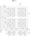
- FIG. 1 is a block diagram illustrating a general configuration of the solid-state imaging device according to the present example.
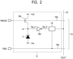
- FIG. 2 is a circuit diagram illustrating a configuration example of a pixel of the solid-state imaging device according to the present example.
- a solid-state imaging device 100 includes a pixel region 10, a vertical scanning circuit 20, a horizontal scanning circuit 30, an output circuit 40, and a control circuit 50.
- a plurality of pixels 12 arranged in a matrix over a plurality of rows and a plurality of columns are provided.
- the number of pixels 12 forming the pixel region 10 is not particularly limited.
- the pixel region 10 may be formed of several thousand rows by several thousand columns of the pixels 12 as seen in general digital cameras.
- the pixel region 10 may be formed of a plurality of pixels 12 arranged in one row or one column.
- the pixel region 10 may be formed of a single pixel 12.
- a control line 14 is arranged extending in a first direction (the horizontal direction in FIG. 1 ).
- Each control line 14 is connected to the pixels 12 aligned in the first direction, respectively, to form a signal line common to these pixels 12.
- the first direction in which the control line 14 extends may be referred to as a row direction or the horizontal direction.
- Each of the control lines 14 may include a plurality of signal lines used for supplying multiple types of control signal to the pixels 12.
- the data line 16 on each column is connected to the horizontal scanning circuit 30.
- the horizontal scanning circuit 30 is a circuit unit that selects a pixel signal of the pixel 12 on each column output on a row-by-row basis from the pixel region 10 and sequentially outputs the selected pixel signal to the output circuit 40.
- the horizontal scanning circuit 30 includes a plurality of holding portions corresponding to a plurality of columns of the pixel region 10 and holds a pixel signal of the pixel 12 on each column output on a row-by-row basis from the pixel region 10 at a holding portion on the corresponding column.
- the horizontal scanning circuit 30 sequentially scans holding portions on respective columns and sequentially outputs pixel signals held in the holding portions on respective columns to the output circuit 40.
- the control circuit 50 is a circuit unit used for supplying control signals that control the operation of the vertical scanning circuit 20 and the horizontal scanning circuit 30 and the timing thereof. Note that at least some of the control signals that control the operation of the vertical scanning circuit 20 and the horizontal scanning circuit 30 and the timing thereof may be supplied from the outside of the solid-state imaging device 100.
- each of the pixels 12 includes a photon detector D, a quench element Mq, a waveform shaper INV, and a signal processing circuit 18.
- the photon detector D may be formed of a photodiode such as an avalanche photo diode (APD) or a single photon avalanche diode (SPAD) in which charges generated by photon incidence are amplified by avalanche breakdown.
- the quench element Mq may be formed of a p-channel MOS transistor, for example.
- the waveform shaper INV may be formed of an inverter circuit, for example.
- the signal processing circuit 18 includes a counter circuit that counts the number of pulses output from the waveform shaper INV
- the anode of the photodiode forming the photon detector D is connected to the node to which a voltage Vss is supplied.
- the cathode of the photodiode forming the photon detector D is connected to the drain (primary node) of the p-channel MOS transistor forming the quench element Mq.
- the source of the p-channel MOS transistor forming the quench element Mq is connected to the node to which a voltage Vdd is supplied.
- the input terminal of the waveform shaper INV is connected to the connection node (node N) between the photon detector D and the quench element Mq.
- the output terminal of the waveform shaper INV is connected to the input terminal of the signal processing circuit 18.
- the output terminal of the signal processing circuit 18 is connected to the data line 16.
- the gate (control node) of the p-channel MOS transistor forming the quench element Mq is supplied with a mode switch signal PMODE from the vertical scanning circuit 20 or the control circuit 50 via a control line 14a.
- the signal processing circuit 18 is supplied with a select signal PSEL from the vertical scanning circuit 20 via a control line 14b.
- the control lines 14a and 14b are signal lines forming the control line 14 described using FIG. 1 .
- the vertical scanning circuit 20 or the control circuit 50 that supplies the mode switch signal PMODE is a control unit that controls the quench element Mq so as to hold an output signal when the photon detector transitions from a Geiger mode to a non-Geiger mode.
- the voltage Vss and the voltage Vdd are set so as to be able to apply, to the photon detector D, a reverse bias voltage which is sufficient for operation in a Geiger mode.
- a negative high voltage is applied as the voltage Vss
- a positive voltage around a power source voltage is applied as the voltage Vdd.
- the photodiode forming the photon detector D is operated in a Geiger mode, that is, used as a single photon avalanche diode (SPAD).
- the photon detector D is in a state where a reverse bias voltage corresponding to the potential difference between the voltage Vdd and the voltage Vss is applied.
- This reverse bias voltage is a voltage higher than the breakdown voltage of the photodiode forming the photon detector D and is high enough to cause avalanche amplification (Geiger mode).
- no carrier as a seed exists in a state where no photon enters the photon detector D, no avalanche amplification occurs, and no current flows in the photon detector D (standby state).
- the mode switch signal PMODE is at a low level, and the quench element Mq is in the detection mode. No photon has entered the photon detector D, the signal Sig_A is a predetermined potential indicating the standby state, and the signal Sig_D is at a low level. Further, at the time t10, the count value of the counter is zero, and the select signal PSEL is at a low level.
- the signal waveforms of the signal Sig_A and the signal Sig_D when the resistance of the quench element Mq is constant are illustrated by dotted lines.
- the potential of the signal Sig_A continuously increases toward the potential of the standby state and is unable to be held at a constant value.
- signal processing that needs to be held for a certain period of time cannot be performed on the signal Sig_A.
- the mode switch signal PMODE is held at the low level.
- the photon detector D can be held in the hold mode, and power consumption can be reduced.
- the process performed by the signal processing circuit 18 is not particularly limited, which may be, for example, a filtering process, signal processing performed simultaneously on the plurality of pixels 12, or the like.
- the operation in the non-hold mode is used when the set ISO sensitivity is relatively high (a high sensitivity mode), and the operation having the hold mode described in the present example is used when the set ISO sensitivity is relatively low (a low sensitivity mode).
- the quench element control circuit 22 detects a rising edge of the signal Sig_D output from the waveform shaper INV and controls a quench element control signal PMq output to the gate of the quench element Mq from a high level to a low level. Further, the quench element control circuit 22 detects a rising edge of the control signal CLK and controls a quench element control signal PMq output to the gate of the quench element Mq from a low level to a high level.
- the control signal CLK is an example of a periodic signal whose signal value changes periodically. Further, in the present embodiment, such a periodic signal is input commonly to the quench element control circuit 22 and the signal processing circuit 18.
- the quench element control signal PMq is at a low level, and the quench element Mq is in the detection mode.
- the signal Sig_A is a predetermined potential illustrating the standby state, and the signal Sig_D is at a low level.
- the count value of the counter is zero, and the select signal PSEL is at a low level.
- the quench element control circuit 22 detects the rising edge of the signal Sig_D supplied from the waveform shaper INV and controls the quench element control signal PMq from the low level to the high level. Thereby, the quench element Mq is in a high resistance state, draining of electrons generated in the photon detector D stops, and the increase of the potential of the signal Sig_A stops. That is, the signal Sig_A is held at a constant value.
- the quench element control circuit 22 maintains the quench element control signal PMq at the high level while the control signal CLK is at the low level.
- the quench element control circuit 22 detects the rising edge of the control signal CLK and controls the quench element control signal PMq from the high level to the low level. Thereby, the quench element Mq is in a low resistance state, that is, in the detection mode. In response to the transition of the quench element Mq to the low resistance state, draining of electrons via the quench element Mq is resumed, and the potential of the signal Sig_A gradually increases to a predetermined potential indicating the standby state.
- the potential of the signal Sig_A gradually increases as electrons generated in the photon detector D are gradually drained via the quench element Mq.
- the signal Sig_D transitions from the low level to the high level.
- the signal processing circuit 18 increments the count value by one in response to the falling edge of the control signal CLK. Thereby, the count value in the counter becomes two.
- the imaging system 200 further includes a signal processing unit 208 that processes an output signal output from the imaging device 201.
- the signal processing unit 208 preforms an AD-conversion that converts an analog signal output by the imaging device 201 into a digital signal.
- the signal processing unit 208 performs various correction and compression other than above, if necessary, and outputting image data.
- An AD-conversion unit which is a part of the signal processing unit 208, may be formed on a semiconductor substrate on which the imaging device 201 is provided or a semiconductor substrate on which the imaging device 201 is not provided. Further, the imaging device 201 and the signal processing unit 208 may be formed on the same semiconductor substrate.
- the imaging system 300 is connected to the vehicle information acquisition device 320 and can acquire vehicle information such as a vehicle speed, a yaw rate, a steering angle, or the like. Further, the imaging system 300 is connected to a control ECU 330, which is a control device that outputs a control signal for causing a vehicle to generate braking force based on a determination result by the collision determination unit 318. Further, the imaging system 300 is also connected to an alert device 340 that issues an alert to the driver based on a determination result by the collision determination unit 318.
Landscapes
- Engineering & Computer Science (AREA)
- Multimedia (AREA)
- Signal Processing (AREA)
- Transforming Light Signals Into Electric Signals (AREA)
- Light Receiving Elements (AREA)
- Solid State Image Pick-Up Elements (AREA)
- Mechanical Engineering (AREA)
Description
- The present invention relates to a solid-state imaging device, a method of driving the solid-state imaging device, an imaging system, and a movable object.
- As photon detector, an avalanche photo diode (APD) and a single photon avalanche diode (SPAD) in which charges generated by photon incidence are amplified by avalanche breakdown are known. These photon detectors are used for capturing or ranging as a photon count sensor that counts the number of detected photons. In general, the sensor using the SPAD is formed of a photon detector, a quench element, a waveform shaper, and a signal processing circuit. An avalanche current generated by the photon detector detecting photons causes a voltage drop through the quench element and generates a photon detection signal. The photon detection signal is shaped into a pulse-like waveform by the waveform shaper, and the shaped signal is input to the signal processing circuit.
Japanese Patent Application Laid-Open No. 2006-179587 - When signal processing is performed on a photon detection signal, it is desirable to hold the photon detection signal for a certain period of time. However, the method disclosed in
Japanese Patent Application Laid-Open No. 2006-179587 GB-A-2 509 545 US-B-9 671 284 US-B-7 115 963 disclosing a circuitry for image sensors with avalanche photodiodes. Further, prior art can be found e.g.in documentGB-A-2 269 O10 US-A-2010/214654 disclosing an apparatus for the detection of light in a scanning microscope, in non-patent literature Cronin, D et al: "Intelligent System for Optimal Hold-Off Time Selection in an Active Quench and Reset IC", IEEE JOURNAL OF SELECTED TOPICS IN QUANTUM ELECTRONICS, IEEE SERVICE CENTER, PISCATAWAY, NJ, US, Vol. 13, No. 4, 1 July 2007 (2007-07-01), pages 911-918, and in documentUS-A-2018/006071 disclosing an imaging device, imaging system and movable object. - The present invention intends to provide a solid-state imaging device and a method of driving the same that can hold a signal detected by a photon detector and perform various signal processing.
- According to aspects of the present invention, provided are a solid-state imaging device according to
claim 1, an imaging system according toclaim 10, and a movable object according toclaim 12. - Further, according to another aspect of the present invention, a method of driving a solid-state imaging device according to claim 9 is provided.
- Further features of the present invention will become apparent from the following description of exemplary embodiments with reference to the attached drawings.
-
-
FIG. 1 is a block diagram illustrating a general configuration of a solid-state imaging device according to a first example useful for understanding the present invention. -
FIG. 2 is a circuit diagram illustrating a configuration example of a pixel of the solid-state imaging device according to the first example useful for understanding the present invention. -
FIG. 3 is a timing chart illustrating a method of driving the solid-state imaging device according to the first example useful for understanding the present invention. -
FIG. 4 is a circuit diagram illustrating a configuration example of a pixel of a solid-state imaging device according to a first embodiment of the present invention. -
FIG. 5 is a timing chart illustrating a method of driving the solid-state imaging device according to the first embodiment of the present invention. -
FIG. 6 is a block diagram illustrating a general configuration of an imaging system according to a second embodiment of the present invention. -
FIG. 7A is a diagram illustrating a configuration example of an imaging system according to a third embodiment of the present invention. -
FIG. 7B is a diagram illustrating a configuration example of a movable object according to the third embodiment of the present invention. - A solid-state imaging device and a method of driving the same according to a first example useful for understanding the present invention will be described with reference to
FIG. 1 to FIG. 3 . - First, the structure of the solid-state imaging device according to the present example will be described by using
FIG. 1 andFIG. 2 .FIG. 1 is a block diagram illustrating a general configuration of the solid-state imaging device according to the present example.FIG. 2 is a circuit diagram illustrating a configuration example of a pixel of the solid-state imaging device according to the present example. - As illustrated in
FIG. 1 , a solid-state imaging device 100 according to the present example includes apixel region 10, a vertical scanning circuit 20, ahorizontal scanning circuit 30, anoutput circuit 40, and acontrol circuit 50. - In the
pixel region 10, a plurality ofpixels 12 arranged in a matrix over a plurality of rows and a plurality of columns are provided. The number ofpixels 12 forming thepixel region 10 is not particularly limited. For example, thepixel region 10 may be formed of several thousand rows by several thousand columns of thepixels 12 as seen in general digital cameras. Alternatively, thepixel region 10 may be formed of a plurality ofpixels 12 arranged in one row or one column. Alternatively, thepixel region 10 may be formed of asingle pixel 12. - On each row of the pixel arrays in the
pixel region 10, acontrol line 14 is arranged extending in a first direction (the horizontal direction inFIG. 1 ). Eachcontrol line 14 is connected to thepixels 12 aligned in the first direction, respectively, to form a signal line common to thesepixels 12. The first direction in which thecontrol line 14 extends may be referred to as a row direction or the horizontal direction. Each of thecontrol lines 14 may include a plurality of signal lines used for supplying multiple types of control signal to thepixels 12. - On each column of the pixel arrays of the
pixel region 10, adata line 16 is arranged extending in a second direction (the vertical direction inFIG. 1 ) crossing the first direction. Eachdata line 16 is connected to thepixels 12 aligned in the second direction, respectively, to form a signal line common to thesepixels 12. The second direction in which thedata line 16 extends may be referred to as a column direction or the vertical direction. Each of thedata lines 16 may include a plurality of signal lines used for transferring digital signals output from thepixels 12 on a bit basis. - The
control line 14 on each row is connected to the vertical scanning circuit 20. The vertical scanning circuit 20 is a circuit unit that supplies control signals used for driving thepixels 12 to thepixels 12 via thecontrol lines 14. The vertical scanning circuit 20 sequentially scans thepixels 12 within thepixel region 10 on a row-by-row basis and outputs a pixel signal of eachpixel 12 to thehorizontal scanning circuit 30 via thedata line 16. - The
data line 16 on each column is connected to thehorizontal scanning circuit 30. Thehorizontal scanning circuit 30 is a circuit unit that selects a pixel signal of thepixel 12 on each column output on a row-by-row basis from thepixel region 10 and sequentially outputs the selected pixel signal to theoutput circuit 40. Thehorizontal scanning circuit 30 includes a plurality of holding portions corresponding to a plurality of columns of thepixel region 10 and holds a pixel signal of thepixel 12 on each column output on a row-by-row basis from thepixel region 10 at a holding portion on the corresponding column. Thehorizontal scanning circuit 30 sequentially scans holding portions on respective columns and sequentially outputs pixel signals held in the holding portions on respective columns to theoutput circuit 40. - The
output circuit 40 is a circuit unit that includes atransmitter circuit 42 and outputs the pixel signal output from thehorizontal scanning circuit 30 to the outside of the solid-state imaging device 100. Thetransmitter circuit 42 may be formed of SERializer/DESerializer (SerDes) transmitter circuit such as a low voltage differential signaling (LVDS) circuit, a scalable low voltage signaling (SLVS) circuit, or the like, for example. Note that an external interface circuit forming theoutput circuit 40 is not particularly limited. - The
control circuit 50 is a circuit unit used for supplying control signals that control the operation of the vertical scanning circuit 20 and thehorizontal scanning circuit 30 and the timing thereof. Note that at least some of the control signals that control the operation of the vertical scanning circuit 20 and thehorizontal scanning circuit 30 and the timing thereof may be supplied from the outside of the solid-state imaging device 100. - As illustrated in
FIG. 2 , each of thepixels 12 includes a photon detector D, a quench element Mq, a waveform shaper INV, and asignal processing circuit 18. The photon detector D may be formed of a photodiode such as an avalanche photo diode (APD) or a single photon avalanche diode (SPAD) in which charges generated by photon incidence are amplified by avalanche breakdown. The quench element Mq may be formed of a p-channel MOS transistor, for example. The waveform shaper INV may be formed of an inverter circuit, for example. Thesignal processing circuit 18 includes a counter circuit that counts the number of pulses output from the waveform shaper INV - The anode of the photodiode forming the photon detector D is connected to the node to which a voltage Vss is supplied. The cathode of the photodiode forming the photon detector D is connected to the drain (primary node) of the p-channel MOS transistor forming the quench element Mq. The source of the p-channel MOS transistor forming the quench element Mq is connected to the node to which a voltage Vdd is supplied. The input terminal of the waveform shaper INV is connected to the connection node (node N) between the photon detector D and the quench element Mq. The output terminal of the waveform shaper INV is connected to the input terminal of the
signal processing circuit 18. The output terminal of thesignal processing circuit 18 is connected to thedata line 16. - The gate (control node) of the p-channel MOS transistor forming the quench element Mq is supplied with a mode switch signal PMODE from the vertical scanning circuit 20 or the
control circuit 50 via acontrol line 14a. Thesignal processing circuit 18 is supplied with a select signal PSEL from the vertical scanning circuit 20 via acontrol line 14b. Thecontrol lines control line 14 described usingFIG. 1 . Note that the vertical scanning circuit 20 or thecontrol circuit 50 that supplies the mode switch signal PMODE is a control unit that controls the quench element Mq so as to hold an output signal when the photon detector transitions from a Geiger mode to a non-Geiger mode. - The voltage Vss and the voltage Vdd are set so as to be able to apply, to the photon detector D, a reverse bias voltage which is sufficient for operation in a Geiger mode. In one example, a negative high voltage is applied as the voltage Vss, and a positive voltage around a power source voltage is applied as the voltage Vdd. In the present example, the photodiode forming the photon detector D is operated in a Geiger mode, that is, used as a single photon avalanche diode (SPAD).
- Thereby, the photon detector D is in a state where a reverse bias voltage corresponding to the potential difference between the voltage Vdd and the voltage Vss is applied. This reverse bias voltage is a voltage higher than the breakdown voltage of the photodiode forming the photon detector D and is high enough to cause avalanche amplification (Geiger mode). However, since no carrier as a seed exists in a state where no photon enters the photon detector D, no avalanche amplification occurs, and no current flows in the photon detector D (standby state).
- Once photons enter the photon detector D in a standby state, carriers excited by incident photons are generated inside the photon detector D. The carriers generated inside the photon detector D are accelerated by a strong electric field inside the photon detector D and causes an avalanche amplification, and a large avalanche current occurs (Geiger mode operation). Such avalanche current flows through the quench element Mq, thereby a voltage drop is caused by the quench element Mq, and the voltage between the terminals of the photon detector D decreases. Thereby, the photon detector D exits the Geiger mode (non-Geiger mode), and the avalanche amplification stops. Carriers at the node (node N) on the cathodes side of the photon detector D are gradually drained via the quench element Mq connected as a load. Thereby, the potential at the node N returns to the initial value again.
- Such a series of operations causes the node N to transition from the standby state to a voltage-dropped state resulted by a flow of a large current in the Geiger mode due to photon incidence and then return to the standby state. Such a potential change at the node N is input to the waveform shaper INV as a signal Sig_A. The waveform shaper INV shapes the waveform of the input signal Sig_A to a pulse-like signal Sig_D and outputs the pulse-like signal Sig_D to the
signal processing circuit 18. Thesignal processing circuit 18 counts the number of pulses superimposed on the signal Sig_D output from the waveform shaper INV Further, thesignal processing circuit 18 performs predetermined signal processing on the signal Sig_D. Thesignal processing circuit 18 outputs an output signal DOUT, which is a signal resulted from signal processing, to thedata line 16 in response to the select signal PSEL output from the vertical scanning circuit 20. - During a period when the mode switch signal PMODE is at a low level (or an on-state or an active state), the quench element Mq is in a relatively low resistance state and operates as a quench resistor (detection mode). On the other hand, during a period when the mode switch signal PMODE is at a high level (or an off-state or an inactive state), the quench element Mq is in a relatively high resistance state, blocks a current flowing into the quench element Mq, and holds the potential of the node N (hold mode).
- Next, a method of driving the solid-state imaging device according to the present example will be described by using
FIG. 3. FIG. 3 is a timing chart illustrating the method of driving the solid-state imaging device according to the present example. The timing chart ofFIG. 3 illustrates the timing when a photon enters the photon detector D, the mode switch signal PMODE, the signal Sig_A, the signal Sig_D, the count value in the counter, the select signal PSEL, and the output signal DOUT. - At time t10, the mode switch signal PMODE is at a low level, and the quench element Mq is in the detection mode. No photon has entered the photon detector D, the signal Sig_A is a predetermined potential indicating the standby state, and the signal Sig_D is at a low level. Further, at the time t10, the count value of the counter is zero, and the select signal PSEL is at a low level.
- At time t11, incidence of a photon occurs. In response, avalanche amplification occurs in the photon detector D with carriers excited with the incident photon being as a seed, and a flow of an avalanche current causes the potential at the node N to decrease. In response to the decrease of the potential at the node N, the potential of the signal Sig_A decreases.
- On and after the time t11, the potential of the signal Sig_A gradually increases as electrons generated in the photon detector D are gradually drained via the quench element Mq.
- In response to the decrease of the potential of the signal Sig_A, the signal Sig_D transitions from the low level to the high level at time t12. The counter of the
signal processing circuit 18 increments the count value by one in response to a rising edge of the signal Sig_D. Thereby, the count value in the counter becomes one. - At time t13, the vertical scanning circuit 20 controls the mode switch signal PMODE from the low level to the high level. Thereby, the quench element Mq is in a high resistance state, draining of electrons generated in the photon detector D stops, and the increase of the potential of the signal Sig_A stops. That is, the signal Sig_A is held at a constant value.
- At time 114, the vertical scanning circuit 20 controls the mode switch signal PMODE from the high level to the low level. Thereby, the quench element Mq is in a low resistance state (on-state), that is, in the detection mode. In response to the transition of the quench element Mq to the low resistance state, draining of electrons via the quench element Mq is resumed, and the potential of the signal Sig_A gradually increases to a predetermined potential indicating the standby state.
- At time t15, when the potential of the signal Sig_A increases to a predetermined value, the signal Sig_D transitions from the high level to the low level and returns to the standby state.
- At subsequent time t16, another incidence of a photon occurs. In response, avalanche amplification occurs in the photon detector D with carriers excited by the incident photon being as a seed, and a flow of an avalanche current causes the potential at the node N to decrease. In response to the decrease of the potential at the node N, the potential of the signal Sig_A decreases.
- On and after the time t16, the potential of the signal Sig_A gradually increases as electrons generated in the photon detector D are gradually drained via the quench element Mq.
- In response to the decrease of the potential of the signal Sig_A due to incidence of a photon, the signal Sig_D transitions from the low level to the high level at time t17. The counter of the
signal processing circuit 18 increments the count value by one in response to the rising edge of the signal Sig_D. Thereby, the count value in the counter becomes two. - At time t18, the vertical scanning circuit 20 controls the mode switch signal PMODE from the low level to the high level. Thereby, the quench element Mq is in a high resistance state, draining of electrons generated in the photon detector D stops, and the increase of the potential of the signal Sig_A stops. That is, the signal Sig_A is held at a constant value.
- At time t19, the vertical scanning circuit 20 controls the select signal PSEL from the low level to the high level. Thereby, the output signal DOUT indicating the count value of two in the counter of the
signal processing circuit 18 is output to thedata line 16. - In
FIG. 3 , the signal waveforms of the signal Sig_A and the signal Sig_D when the resistance of the quench element Mq is constant (detection mode) are illustrated by dotted lines. In this case, the potential of the signal Sig_A continuously increases toward the potential of the standby state and is unable to be held at a constant value. Thus, signal processing that needs to be held for a certain period of time cannot be performed on the signal Sig_A. - In contrast, in the method of driving the solid-state imaging device according to the present example, the potential of the signal Sig_A can be held at a constant level during the period of time t13 to time t14 and a period on and after time t18 in which the mode switch signal PMODE is controlled to the high level. Therefore, according to the present example, signal processing that needs to be held for a certain period of time can be performed on the signal Sig A.
- That is, when signal processing that needs to be held for a certain period of time is performed on the signal Sig_A, the mode switch signal PMODE is held at the low level. Thereby, during a period in which the
signal processing circuit 18 performs signal processing, that is, a period in which thesignal processing circuit 18 does not accept input, the photon detector D can be held in the hold mode, and power consumption can be reduced. The process performed by thesignal processing circuit 18 is not particularly limited, which may be, for example, a filtering process, signal processing performed simultaneously on the plurality ofpixels 12, or the like. - Further, when the
signal processing circuit 18 performs only the process that requires substantially no period for holding an input signal, for example, a simple counting process, it is possible to set a longer period for detecting photons and increase detection sensitivity of photons by setting a shorter period of the hold mode. - Further, an operation in a non-hold mode in which the mode switch signal PMODE is maintained at the high level during an integration period from the start to the end of integration of count values in the counter may be used. This integration period is a period determined from an exposure condition such as a framerate, an aperture, a set ISO sensitivity, a shutter speed, or the like. The solid-state imaging device of the present example can perform switching between an operation having the hold mode described in the present example and an operation in the non-hold mode.
- An example of selection of the operation having the hold mode described in the present example and the operation in the non-hold mode will be described. For example, the operation in the non-hold mode is used when the set ISO sensitivity is relatively high (a high sensitivity mode), and the operation having the hold mode described in the present example is used when the set ISO sensitivity is relatively low (a low sensitivity mode).
- When the set ISO sensitivity is set relatively high, it is often the case of capturing a low light amount capturing scene. In such a low light amount scene, it is preferable to shorten a period in which the photon detector D is in a non-Geiger mode to enable detection of a small amount of incident photons.
- On the other hand, when the set ISO sensitivity is set relatively low, it is often the case of capturing a high light amount capturing scene. When operated in the non-hold mode, an SPAD tends to require time to return to a Geiger mode from a non-Geiger mode and be unable to detect photons entering the photon detector D during the time period. Therefore, increase of a signal value of the output signal DOUT of the
pixel 12 no longer responds to increase of an incident light amount. That is, the linearity of the output signal DOUT of thepixel 12 relative to an incident light amount decreases as the incident light amount increases. - Accordingly, in such a high light amount scene, during the operation having the hold mode described in the present example, that is, the integration period, a period in which the mode switch signal PMODE is at the high level is provided for n times. Each of the n times of periods is referred to as a sub-integration period. By deriving the ratio of a count value to the number n, it is possible to estimate the amount of light entering the photon detector D. That is, in each of the n times of sub-integration periods, as the frequency of a photon entering the photon detector D increases, the count value in the counter approaches n. For example, when the count value becomes n, this indicates that photons enter the photon detector D in all the sub-integration periods, which indicates that the amount of light entering the photon detector D is large.
- When a signal of the solid-state imaging element is used to generate an image, the luminance at an image position corresponding to the
pixel 12 can be defined as the maximum value (typically, white). In such a way, by using the mode switch signal PMODE to provide sub-integration periods, it is possible to derive a ratio of the count value in the counter relative to the number of times of sub-integration periods. Thereby, the linearity of a signal value of the output signal DOUT of thepixel 12 relative to an increase of the incident light mount can be increased. - As discussed above, according to the present example, a signal detected by the photon detector can be held for a desired time period, and various signal processing can be performed in the post-stage signal processing circuit.
- A solid-state imaging device and a method of driving the same according to a first embodiment of the present invention will be described with reference to
FIG. 4 and -
FIG. 5 . The same components as those in the solid-state imaging device according to the first example will be labeled with the same references, and the description thereof will be omitted or simplified. - First, the structure of the solid-state imaging device according to the present embodiment will be described by using
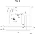
FIG. 4. FIG. 4 is a circuit diagram illustrating a configuration example of a pixel of the solid-state imaging device according to the present embodiment. - As illustrated in
FIG. 4 , thepixel 12 of the solid-state imaging device according to the present embodiment further includes a quenchelement control circuit 22 in addition to the photon detector D, the quench element Mq, a waveform shaper INV, and thesignal processing circuit 18. Other configurations of the solid-state imaging device according to the present embodiment are basically the same as the solid-state imaging device according to the first example. - The anode of the photodiode forming the photon detector D is connected to the node to which a voltage Vss is supplied. The cathode of the photodiode forming the photon detector D is connected to the drain of the p-channel MOS transistor forming the quench element Mq. The source of the p-channel MOS transistor forming the quench element Mq is connected to the node to which a voltage Vdd is supplied. The gate of the p-channel MOS transistor forming the quench element Mq is connected to the output terminal of the quench
element control circuit 22. The input terminal of the waveform shaper INV is connected to the connection node (node N) between the photon detector D and the quench element Mq. The output terminal of the waveform shaper INV is connected to the input terminal of thesignal processing circuit 18 and the input terminal of the quenchelement control circuit 22. The output terminal of thesignal processing circuit 18 is connected to thedata line 16. - The
signal processing circuit 18 is supplied with the select signal PSEL from the vertical scanning circuit 20 via thecontrol line 14b. Further, thesignal processing circuit 18 and the quenchelement control circuit 22 are supplied with a control signal CLK from the vertical scanning circuit 20 or thecontrol circuit 50 via acontrol line 14c. The control lines 14b and 14c are signal lines forming thecontrol line 14 described usingFIG. 1 . The control signal CLK is a timing signal that determines operation timings of the solid-state imaging device, which may be a signal based on a clock signal, for example. Note that the quenchelement control circuit 22 is a control unit that controls the quench element so that the photon detector holds an output signal when transitioning from a Geiger mode to a non-Geiger mode. - As described in the first example, the node N transitions from the standby state to a voltage-dropped state resulted by a flow of a large current in the Geiger mode due to photon incidence and then returns to the standby state. Such a potential change at the node N is input to the waveform shaper INV as a signal Sig_A. The waveform shaper INV shapes the waveform of the input signal Sig_A to a pulse-like signal Sig_D and outputs the pulse-like signal Sig_D to the
signal processing circuit 18 and the quenchelement control circuit 22. - The
signal processing circuit 18 performs counting of the number of pulses or predetermined signal processing in synchronization with the control signal CLK. For example, when the signal Sig_D is at a high level at the timing of a falling edge of the control signal CLK, thesignal processing circuit 18 counts this pulse. Further, thesignal processing circuit 18 performs predetermined signal processing on the signal Sig_D in accordance with the timing of the control signal CLK. Thesignal processing circuit 18 outputs an output signal DOUT, which is a signal resulted from signal processing, to thedata line 16 in response to the select signal PSEL output from the vertical scanning circuit 20. - The quench
element control circuit 22 detects a rising edge of the signal Sig_D output from the waveform shaper INV and controls a quench element control signal PMq output to the gate of the quench element Mq from a high level to a low level. Further, the quenchelement control circuit 22 detects a rising edge of the control signal CLK and controls a quench element control signal PMq output to the gate of the quench element Mq from a low level to a high level. The control signal CLK is an example of a periodic signal whose signal value changes periodically. Further, in the present embodiment, such a periodic signal is input commonly to the quenchelement control circuit 22 and thesignal processing circuit 18. - During a period when the quench element control signal PMq is at a high level, the quench element Mq is in a relatively low resistance state and operates as a quench resistor (detection mode). On the other hand, during a period when the quench element control signal PMq is at a low level, the quench element Mq is in a relatively high resistance state, blocks a current flowing to the quench element Mq, and holds the potential of the node N (hold mode).
- Next, a method of driving the solid-state imaging device according to the present embodiment will be described by using
FIG. 5. FIG. 5 is a timing chart illustrating the drive method of the solid-state imaging device according to the present embodiment. The timing chart ofFIG. 5 illustrates the timing when a photon enters the photon detector D, the control signal CLK, the quench element control signal PMq, the signal Sig_A, the signal Sig_D, the count value in the counter, the select signal PSEL, and the output signal DOUT. - At time t20, the quench element control signal PMq is at a low level, and the quench element Mq is in the detection mode. No photon has entered the photon detector D, the signal Sig_A is a predetermined potential illustrating the standby state, and the signal Sig_D is at a low level. Further, at the time t20, the count value of the counter is zero, and the select signal PSEL is at a low level.
- At time t21, incidence of a photon occurs. In response, avalanche amplification occurs in the photon detector D with carriers excited by the incident photon being as a seed, and a flow of an avalanche current causes the potential at the node N to decrease. In response to the decrease of the potential at the node N, the potential of the signal Sig_A decreases.
- On and after the time t21, the potential of the signal Sig_A gradually increases as electrons generated in the photon detector D are gradually drained via the quench element Mq.
- At time t22, in response to the decrease of the potential of the signal Sig_A, the signal Sig_D transitions from the low level to the high level.
- At time t23, the quench
element control circuit 22 detects the rising edge of the signal Sig_D supplied from the waveform shaper INV and controls the quench element control signal PMq from the low level to the high level. Thereby, the quench element Mq is in a high resistance state, draining of electrons generated in the photon detector D stops, and the increase of the potential of the signal Sig_A stops. That is, the signal Sig_A is held at a constant value. The quenchelement control circuit 22 maintains the quench element control signal PMq at the high level while the control signal CLK is at the low level. - At time t24, the
signal processing circuit 18 increments the count value by one in response to the falling edge of the control signal CLK. Thereby, the count value in the counter becomes one. - At time t25, the quench
element control circuit 22 detects the rising edge of the control signal CLK and controls the quench element control signal PMq from the high level to the low level. Thereby, the quench element Mq is in a low resistance state, that is, in the detection mode. In response to the transition of the quench element Mq to the low resistance state, draining of electrons via the quench element Mq is resumed, and the potential of the signal Sig_A gradually increases to a predetermined potential indicating the standby state. - At time t26, when the potential of the signal Sig_A increases to a predetermined value, the signal Sig_D transitions from the high level to the low level, and returns to the standby state.
- At subsequent time t27, another incidence of a photon occurs. In response, avalanche amplification occurs in the photon detector D with carriers excited by the incident photon being as a seed, and a flow of an avalanche current causes the potential at the node N to decrease. In response to the decrease of the potential at the node N, the potential of the signal Sig_A decreases.
- On and after the time t27, the potential of the signal Sig_A gradually increases as electrons generated in the photon detector D are gradually drained via the quench element Mq.
- At time t28, in response to the decrease of the potential of the signal Sig_A due to incidence of a photon, the signal Sig_D transitions from the low level to the high level.
- At time t29, the quench
element control circuit 22 detects the rising edge of the signal Sig_D supplied from thesignal processing circuit 18 and controls the quench element control signal PMq from the low level to the high level. Thereby, the quench element Mq is in a high resistance state, draining of electrons generated in the photon detector D stops, and the increase of the potential of the signal Sig_A stops. That is, the signal Sig_A is held at a constant value. - At time t30, the
signal processing circuit 18 increments the count value by one in response to the falling edge of the control signal CLK. Thereby, the count value in the counter becomes two. - At time t31, the vertical scanning circuit 20 controls the select signal PSEL from the low level to the high level. Thereby, the output signal DOUT indicating the count value of two in the counter of the
signal processing circuit 18 is output to thedata line 16. - Note that, while the case where incidence of a photon occurs in a period in which the control signal CLK is at a high level has been assumed in the example described above, the quench element Mq is in a hold mode when incidence of a photon occurs in a period in which the control signal CLK is at a high level, and the signals Sig_A and Sig_D do not change. That is, in the solid-state imaging device according to the present embodiment, detection of a photon and signal processing on the signal Sig_D are enabled in synchronization with the control signal CLK.
- In
FIG. 5 , the signal waveforms of the signal Sig_A and the signal Sig_D when the resistance of the quench element Mq is constant (detection mode) are illustrated by doted lines. In this case, the potential of the signal Sig_A continuously increases toward the potential of the standby state and is unable to be held at a constant value. Thus, signal processing that needs to be held for a certain period of time cannot be performed on the signal Sig_A. - In contrast, in the method of driving the solid-state imaging device according to the present embodiment, the potential of the signal Sig_A can be held at a constant level during the period of time t23 to time t25 and a period on and after time t29 in which the quench element control signal PMq is controlled to the high level. Therefore, according to the present embodiment, signal processing that needs to be held for a certain period of time can be performed on the signal Sig_A.
- In particular, in the present embodiment, since the quench element Mq is switched to the hold mode in accordance with the level of the signal Sig_D, switching of the quench element Mq to the hold mode can be performed independently on a
pixel 12 basis immediately after photon detection. Therefore, the present embodiment is a more preferable form than the first example in terms of reduction of consumption power. - Further, since the quench element Mq is switched to the detection mode when the control signal CLK becomes a high level, the present embodiment is a more preferable form also when signal processing across a plurality of
pixels 12 is performed, such as when detection results at a certain timing of the plurality ofpixels 12 are intended to be acquired at the same time, for example. - Further, while the same control signal CLK is input to the quench
element control circuit 22 and thesignal processing circuit 18 in the present embodiment, the embodiment is not limited to this example. For example, separate control signals may be supplied to thesignal processing circuit 18 and the quenchelement control circuit 22. Further, as another example, a frequency division circuit, which divides the frequency of the control signal CLK, is provided in the pre-stage of the quenchelement control circuit 22. Further, a signal resulted by dividing the frequency of the control signal CLK may be input from the frequency division circuit to the quenchelement control circuit 22. Including the above form in which a signal resulted by dividing the frequency of the control signal CLK is input to the quenchelement control circuit 22, a form in which a signal based on the control signal CLK is input to the quenchelement control circuit 22 is preferable. - As discussed above, according to the present embodiment, a signal detected by the photon detector can be held for a desired time period, and various signal processing can be performed on the post-stage signal processing circuit. Further, detection of photons or signal processing can be performed in response to a timing signal, and a synchronous system of photo-counting can be realized.
- Note that, also in the present embodiment, as described in the first example, an operation having the hold mode described in the present embodiment or an operation in the non-hold mode can be appropriately used. For example, the operation in the non-hold mode is used when the set ISO sensitivity is relatively high (a high sensitivity mode), and the operation having the hold mode described in the present embodiment is used when the set ISO sensitivity is relatively low (a low sensitivity mode).
- During the operation having the hold mode described in the present embodiment, that is, the integration period, n times of sub-integration periods are provided. In the present embodiment, these sub-integration periods are respective periods in which the control signal CLK is at the high level. By deriving the ratio of a count value to the number n, it is possible to estimate the amount of light entering the photon detector D. That is, in each of the n times of sub-integration periods, as the frequency of a photon entering the photon detector D increases, the count value in the counter approaches n. For example, when the count value becomes n, this indicates that photons enter the photon detector D in all the sub-integration periods, which indicates that the amount of light entering the photon detector D is large.
- When a signal of the solid-state imaging element is used to generate an image, the luminance at an image position corresponding to the
pixel 12 can be defined as the maximum value (typically, white). In such a way, by using the mode switch signal PMODE to provide sub-integration periods, it is possible to derive a ratio of the count value in the counter relative to the number of times of sub-integration periods. Thereby, the linearity of a signal value of the output signal DOUT of thepixel 12 relative to an increase of the incident light mount can be increased. Further, an increase in the frequency of the control signal CLK allows the linearity to be higher. - An imaging system according to a second embodiment of the present invention will be described with reference to
FIG. 6. FIG. 6 is a block diagram illustrating a general configuration of the imaging system according to the present embodiment. - The solid-
state imaging device 100 described in the first example and the first embodiment described above can be applied to various imaging systems. Examples of applicable imaging systems may include a digital still camera, a digital camcorder, a surveillance camera, a copying machine, a fax machine, a mobile phone, an on-vehicle camera, an observation satellite, and the like. In addition, a camera module including an optical system such as a lens and an imaging device is also included in the imaging system.FIG. 6 illustrates a block diagram of a digital still camera as an example out of these examples. - The
imaging system 200 illustrated as an example inFIG. 6 includes animaging device 201, alens 202 that captures an optical image of an object onto theimaging device 201, anaperture 204 for changing a light amount passing through thelens 202, and abarrier 206 for protecting thelens 202. Thelens 202 and theaperture 204 form an optical system that converges a light onto theimaging device 201. Theimaging device 210 is the solid-state imaging device 100 described in the first example (not claimed) or the first embodiment and converts an optical image captured by thelens 202 into image data. - The
imaging system 200 further includes asignal processing unit 208 that processes an output signal output from theimaging device 201. Thesignal processing unit 208 preforms an AD-conversion that converts an analog signal output by theimaging device 201 into a digital signal. In addition, thesignal processing unit 208 performs various correction and compression other than above, if necessary, and outputting image data. An AD-conversion unit, which is a part of thesignal processing unit 208, may be formed on a semiconductor substrate on which theimaging device 201 is provided or a semiconductor substrate on which theimaging device 201 is not provided. Further, theimaging device 201 and thesignal processing unit 208 may be formed on the same semiconductor substrate. - The
imaging system 200 further includes amemory unit 210 for temporarily storing image data therein and an external interface unit (external I/F unit) 212 for communicating with an external computer or the like. Theimaging system 200 further includes astorage medium 214 such as a semiconductor memory for performing storage or readout of imaging data and a storage medium control interface unit (storage medium control I/F unit) 216 for performing storage or readout on thestorage medium 214. Note that thestorage medium 214 may be embedded in theimaging system 200 or may be removable. - The
imaging system 200 further includes a general control/operation unit 218 that controls various operations and the entire digital still camera and atiming generation unit 220 that outputs various timing signals to theimaging device 201 and thesignal processing unit 208. Here, the timing signal or the like may be input from the outside, and theimaging system 200 may include at least theimaging device 201 and thesignal processing unit 208 that processes an output signal output from theimaging device 201. - The
imaging device 201 outputs an imaging signal to thesignal processing unit 208. Thesignal processing unit 208 performs predetermined signal processing on an imaging signal output from theimaging device 201 and outputs image data. Thesignal processing unit 208 uses an imaging signal to generate an image. - As discussed above, according to the present embodiment, the imaging system to which the solid-
state imaging device 100 according to the first example (not claimed) or first embodiment is applied can be realized. - An imaging system and a movable object according to a third embodiment of the present invention will be described with reference to
FIG. 7A and FIG. 7B. FIG. 7A is a diagram illustrating a configuration of an imaging system according to the present embodiment.FIG. 7B is a diagram illustrating a configuration of a movable object according to the present embodiment. -
FIG. 7A illustrates an example of an imaging system related to an on-vehicle camera. Theimaging system 300 includes animaging device 310. Theimaging device 310 is the solid-state imaging device 100 described in any of the above first example (not claimed) and first embodiment. Theimaging system 300 includes animage processing unit 312 that performs image processing on a plurality of image data acquired by theimaging device 310 and aparallax acquisition unit 314 that calculates a parallax (a phase difference of parallax images) from the plurality of image data acquired by theimaging system 300. Further, theimaging system 300 includes adistance acquisition unit 316 that calculates a distance to the object based on the calculated parallax and acollision determination unit 318 that determines whether or not there is a collision possibility based on the calculated distance. Here, theparallax acquisition unit 314 and thedistance acquisition unit 316 are an example of a distance information acquisition unit that acquires distance information on the distance to the object. That is, the distance information is information on a parallax, a defocus amount, a distance to an object, or the like. Thecollision determination unit 318 may use any of the distance information to determine the collision possibility. The distance information acquisition unit may be implemented by dedicatedly designed hardware or may be implemented by a software module. Further, the distance information acquisition unit may be implemented by a Field Programmable Gate Array (FPGA), an Application Specific Integrated Circuit (ASIC), or the like, or may be implemented by combination thereof. - The
imaging system 300 is connected to the vehicleinformation acquisition device 320 and can acquire vehicle information such as a vehicle speed, a yaw rate, a steering angle, or the like. Further, theimaging system 300 is connected to acontrol ECU 330, which is a control device that outputs a control signal for causing a vehicle to generate braking force based on a determination result by thecollision determination unit 318. Further, theimaging system 300 is also connected to analert device 340 that issues an alert to the driver based on a determination result by thecollision determination unit 318. For example, when the collision probability is high as the determination result of thecollision determination unit 318, thecontrol ECU 330 performs vehicle control to avoid a collision or reduce damage by applying a brake, pushing back an accelerator, suppressing engine power, or the like. Thealert device 340 alerts a user by sounding an alert such as a sound, displaying alert information on a display of a car navigation system or the like, providing vibration to a seat belt or a steering wheel, or the like. - In the present embodiment, an area around a vehicle, for example, a front area or a rear area is captured by using the
imaging system 300.FIG. 7B illustrates the imaging system when a front area of a vehicle (a capturing area 350) is captured. The vehicleinformation acquisition device 320 transmits an instruction to theimaging system 300 or theimaging device 310. Such a configuration can further improve the ranging accuracy. - Although the example of control for avoiding a collision to another vehicle has been described, the embodiment is applicable to automatic driving control for following another vehicle, automatic driving control for not going out of a traffic lane, or the like. Furthermore, the imaging system is not limited to a vehicle such as the subject vehicle and can be applied to a movable object (moving apparatus) such as a ship, an airplane, or an industrial robot, for example. In addition, the imaging system can be widely applied to a device which utilizes object recognition, such as an intelligent transportation system (ITS), without being limited to movable objects.
- The present invention is not limited to the embodiments described above, and various modifications are possible.
- Further, while a solid-state imaging device in which the
pixels 12 are arranged two-dimensionally inside thepixel region 10 has been assumed in the embodiments described above, the arrangement of thepixels 12 is not limited to be two-dimensional. For example, a solid-state imaging device may be formed of asingle pixel 12, or thepixels 12 may be arranged one-dimensionally or three-dimensionally. - Further, while each of the
control lines 14 is used as a signal line common to all thepixels 12 on each row and each of the data lines 16 is used as a signal line common to all thepixels 12 on each column in the embodiments described above, the arrangement of thecontrol lines 14 and the data lines 16 is not limited thereto. For example, acommon control line 14 or acommon data line 16 may be arranged on a block basis in a unit of i row(s) by j column(s) (i and j are both natural numbers). - Further, the imaging systems illustrated in the above second and third embodiments are examples of an imaging system to which the photoelectric conversion device of the present invention may be applied, and an imaging system to which the photoelectric conversion device of the present invention can be applied is not limited to the configuration illustrated in
FIG. 6 andFIG. 7A . - While the present invention has been described with reference to exemplary embodiments, it is to be understood that the invention is not limited to the disclosed exemplary embodiments but by the scope of the following claims.
Claims (12)
- A solid-state imaging device comprising:a photon detector (D) that operates in a Geiger mode and outputs an analog output signal as a result of an avalanche amplification in accordance with the incidence of a photon;a quench element (Mq) that causes the photon detector to transition to a non-Geiger mode in which the avalanche amplification does not occur; anda signal processing circuit (18) that performs a predetermined process on the output signal,characterized bya control unit (22) that is supplied with a control signal (CLK) and a digital signal which is shaped into a pulse-like waveform from the analog output signal from the photon detector and switches, in accordance with the control signal and the digital signal, the quench element between a state in which the quench element has a relatively low resistance and the photon detector detects the photon in the Geiger mode, and a hold state in which the quench element has a relatively high resistance and a potential of a node between the photon detector and the quench element is controlled to hold the photon detector in the non-Geiger mode, whereinthe control unit (22) switches the quench element from the low resistance state to the high resistance state when the photon detector transitions from the Geiger mode to the non-Geiger mode, and then switches the quench element from the high resistance state to the low resistance state;the control signal is a periodic signal whose signal value changes periodically from a first level to a second level; andthe signal processing circuit performs the predetermined process in synchronization with the control signal.
- The solid-state imaging device according to claim 1 , wherein the control unit switches the quench element from the high resistance state to the low resistance state in response to transition of the control signal, which determines an operation timing, from the first level to the second level.
- The solid-state imaging device according to claim 2, wherein the control unit sets the quench element in the high resistance state during a period in which the control signal is at the first level.
- The solid-state imaging device according to any one of claims 1 to 3, wherein the quench element is a transistor, the low resistance state corresponds to a state where the transistor is in an on-state, and the high resistance state corresponds to a state where the transistor is in an off-state.
- The solid-state imaging device according to any one of claims 1 to 4,wherein the signal processing circuit includes a counter that performs integration of the number of times of a change of the output signal,wherein the solid-state imaging device is capable of selecting an operation mode out of a plurality of operation modes including the hold state and the non-hold state,wherein in the hold state, the control unit controls the quench element so that the photon detector holds the output signal when transitioning from the Geiger mode to the non-Geiger mode over a period from start to end of the integration performed by the counter, andwherein in the non-hold state, the control unit controls the quench element so that the photon detector does not hold the output signal when transitioning from the Geiger mode to the non-Geiger mode over a period from start to end of the integration performed by the counter and the photon detector transitions from the non-Geiger mode to the Geiger mode.
- The solid-state imaging device according to any of claims 1 to 5, wherein:the photon detector (D) outputs the output signal resulting from avalanche amplification of the photon;the quench element comprises a transistor (Mq) having a drain connected to the photon detector (D) and a source connected to a node to which a voltage VDD is supplied;the control unit (22) supplies a signal to the gate of the transistor to cause the transistor to be in the relatively low resistance state at a set predetermined cycle, whereinthe photon may be detected when the transistor is in the relatively low resistance state.
- The solid-state imaging device according to claim 6, wherein the control signal is a signal resulting from dividing the frequency of a clock signal.
- The solid-state imaging device according to claim 7, wherein the analog output signal is held at a constant value by the quench element in the hold state.
- A method of driving a solid-state imaging device including a photon detector (D) that outputs an analog output signal as a result of an avalanche amplification in accordance with an incidence of a photon if the photon detector operates in a Geiger mode; a quench element (Mq) that causes the photon detector to transition to a non-Geiger mode in which the avalanche amplification does not occur; and a signal processing circuit (18) that performs a predetermined process on the output signal in synchronization with a control signal (CLK), the method being characterized by comprising:when the photon detector transitions from the Geiger mode to the non-Geiger mode in accordance with a digital signal which is shaped into a pulse-like waveform from the analog output signal from the photon detector and the control signal (CLK), switching the quench element from a relatively low resistance state to a relatively high resistance state, whereinthe quench element is switched from the low resistance state to the high resistance state such that a potential of a node between the photon detector and the quench element is controlled to hold the photon detector in the non-Geiger mode when the photon detector transitions from the Geiger mode to the non-Geiger mode, and then the quench element is switched from the high resistance state to the low resistance state;the control signal is a periodic signal whose signal value changes periodically from a first level to a second level.
- An imaging system comprising a plurality of pixels each including a solid-state imaging device according to any one of claims 1 to 8.
- The imaging system according to claim 10, further comprising
a signal processing unit that processes a signal output from the solid-state imaging devices. - A movable object comprising:the solid-state imaging device according to any one of claims 1 to 8;a distance information acquisition unit that acquires distance information on a distance to an object, from parallax images based on a signal from the solid-state imaging device; anda control unit that controls the movable object based on the distance information.
Applications Claiming Priority (1)
| Application Number | Priority Date | Filing Date | Title |
|---|---|---|---|
| JP2018067058A JP7089390B2 (en) | 2018-03-30 | 2018-03-30 | Photoelectric conversion device and its driving method |
Publications (2)
| Publication Number | Publication Date |
|---|---|
| EP3547668A1 EP3547668A1 (en) | 2019-10-02 |
| EP3547668B1 true EP3547668B1 (en) | 2024-07-10 |
Family
ID=65766901
Family Applications (1)
| Application Number | Title | Priority Date | Filing Date |
|---|---|---|---|
| EP19162140.8A Active EP3547668B1 (en) | 2018-03-30 | 2019-03-12 | Solid-state imaging device, method of driving said solid-state imaging device, movable object comprising said solid-state imaging device |
Country Status (4)
| Country | Link |
|---|---|
| US (1) | US10971539B2 (en) |
| EP (1) | EP3547668B1 (en) |
| JP (1) | JP7089390B2 (en) |
| CN (1) | CN110324544B (en) |
Families Citing this family (10)
| Publication number | Priority date | Publication date | Assignee | Title |
|---|---|---|---|---|
| JP7393162B2 (en) | 2019-09-09 | 2023-12-06 | キヤノン株式会社 | Photoelectric conversion device |
| JP7427417B2 (en) | 2019-10-25 | 2024-02-05 | キヤノン株式会社 | Photoelectric conversion device, photoelectric conversion system, moving object, inspection method for photoelectric conversion device |
| TWI888471B (en) * | 2020-02-27 | 2025-07-01 | 日商索尼半導體解決方案公司 | Light receiving element, optical device and electronic device |
| CN116457687A (en) * | 2020-09-11 | 2023-07-18 | 感应光子公司 | Clock active quench/recharge and gain cell memory pixel |
| US11784195B2 (en) * | 2021-01-07 | 2023-10-10 | Canon Kabushiki Kaisha | Photoelectric conversion apparatus and photodetection system |
| JP7760320B2 (en) | 2021-10-08 | 2025-10-27 | キヤノン株式会社 | Photoelectric conversion device |
| JP7775021B2 (en) * | 2021-10-20 | 2025-11-25 | キヤノン株式会社 | Photoelectric conversion device, photoelectric conversion system, mobile object, equipment |
| JP7725332B2 (en) * | 2021-10-20 | 2025-08-19 | キヤノン株式会社 | Photoelectric conversion device, photoelectric conversion system, mobile object, equipment |
| JP7703464B2 (en) | 2022-01-28 | 2025-07-07 | キヤノン株式会社 | Photoelectric conversion device, control method thereof, and program |
| JP7791251B2 (en) * | 2023-08-28 | 2025-12-23 | キヤノン株式会社 | Photoelectric conversion device and photoelectric conversion system |
Family Cites Families (37)
| Publication number | Priority date | Publication date | Assignee | Title |
|---|---|---|---|---|
| GB2269010B (en) | 1992-07-25 | 1996-01-17 | Roke Manor Research | Improvements in or relating to photon counters |
| IT1316793B1 (en) * | 2000-03-09 | 2003-05-12 | Milano Politecnico | MONOLITHIC CIRCUIT OF ACTIVE SHUTDOWN AND ACTIVE RESTORATION AVALANCHE PERFOTODIODI |
| AU2002238699A1 (en) | 2002-02-08 | 2003-09-02 | Qinetiq Limited | Photodetector circuit |
| AU2003289994A1 (en) | 2002-12-09 | 2004-06-30 | Carlos J.R.P. Augusto | Circuitry for image sensors with avalanche photodiodes |
| US7858917B2 (en) * | 2003-05-02 | 2010-12-28 | Massachusetts Institute Of Technology | Digital photon-counting geiger-mode avalanche photodiode solid-state monolithic intensity imaging focal-plane with scalable readout circuitry |
| JP4155971B2 (en) | 2004-12-21 | 2008-09-24 | アンリツ株式会社 | APD photon detector |
| US7361882B2 (en) * | 2005-04-14 | 2008-04-22 | Sensors Unlimited, Inc. | Method and apparatus for providing non-linear, passive quenching of avalanche currents in Geiger-mode avalanche photodiodes |
| GB2426575A (en) | 2005-05-27 | 2006-11-29 | Sensl Technologies Ltd | Photon detector using controlled sequences of reset and discharge of a capacitor to sense photons |
| US7897906B2 (en) | 2007-03-23 | 2011-03-01 | Excelitas Canada Inc. | Double quench circuit for an avalanche current device |
| DE102007024074B4 (en) | 2007-05-22 | 2022-09-15 | Leica Microsystems Cms Gmbh | microscope |
| TWI441512B (en) * | 2009-10-01 | 2014-06-11 | 新力股份有限公司 | Image acquisition device and camera system |
| US8716643B2 (en) * | 2010-09-06 | 2014-05-06 | King Abdulaziz City Science And Technology | Single photon counting image sensor and method |
| GB2487958A (en) * | 2011-02-10 | 2012-08-15 | St Microelectronics Res & Dev | A multi-mode photodetector pixel |
| JP5791338B2 (en) | 2011-04-07 | 2015-10-07 | キヤノン株式会社 | Solid-state imaging device and driving method thereof |
| JP5901212B2 (en) | 2011-10-07 | 2016-04-06 | キヤノン株式会社 | Photoelectric conversion system |
| JP5484422B2 (en) | 2011-10-07 | 2014-05-07 | キヤノン株式会社 | Solid-state imaging device |
| JP5499011B2 (en) | 2011-11-17 | 2014-05-21 | 富士重工業株式会社 | Outside environment recognition device and outside environment recognition method |
| CN102538988B (en) * | 2012-02-08 | 2014-05-07 | 南京邮电大学 | Quenching and reading circuit for single photon avalanche diode imaging device |
| JP5893573B2 (en) | 2012-02-09 | 2016-03-23 | キヤノン株式会社 | Solid-state imaging device |
| GB2509545A (en) | 2013-01-08 | 2014-07-09 | Isis Innovation | Photo detector comprising SPAD cell array |
| JP6319946B2 (en) | 2013-04-18 | 2018-05-09 | キヤノン株式会社 | Solid-state imaging device and imaging system |
| JP6100074B2 (en) | 2013-04-25 | 2017-03-22 | キヤノン株式会社 | Photoelectric conversion device and imaging system |
| JP6274788B2 (en) | 2013-08-28 | 2018-02-07 | キヤノン株式会社 | Imaging apparatus, imaging system, and driving method of imaging apparatus |
| JP6285168B2 (en) | 2013-12-17 | 2018-02-28 | 株式会社デンソー | Radar equipment |
| JP6239975B2 (en) | 2013-12-27 | 2017-11-29 | キヤノン株式会社 | Solid-state imaging device and imaging system using the same |
| US9312401B2 (en) * | 2014-01-15 | 2016-04-12 | Omnivision Technologies, Inc. | Single photon avalanche diode imaging sensor for complementary metal oxide semiconductor stacked chip applications |
| JP6246004B2 (en) | 2014-01-30 | 2017-12-13 | キヤノン株式会社 | Solid-state imaging device |
| JP6528447B2 (en) * | 2014-02-25 | 2019-06-12 | 株式会社リコー | Disparity calculation system and distance measuring device |
| KR102409952B1 (en) | 2014-04-07 | 2022-06-17 | 삼성전자주식회사 | High resolution, high frame rate, low power image sensor |
| JP6482186B2 (en) | 2014-05-23 | 2019-03-13 | キヤノン株式会社 | Imaging apparatus and driving method thereof |
| EP3164683B1 (en) * | 2014-07-02 | 2023-02-22 | The John Hopkins University | Photodetection circuit |
| CN106716994B (en) * | 2014-09-19 | 2020-01-17 | 松下知识产权经营株式会社 | Solid-state imaging device |
| JP6523046B2 (en) | 2015-05-29 | 2019-05-29 | シャープ株式会社 | Optical sensor |
| US9671284B1 (en) * | 2016-01-14 | 2017-06-06 | Kiskeya Microsystems Llc | Single-photon avalanche diode circuit with variable hold-off time and dual delay regime |
| JP6711634B2 (en) | 2016-02-16 | 2020-06-17 | キヤノン株式会社 | Imaging device, driving method of imaging device, and imaging system |
| JP6774224B2 (en) | 2016-05-26 | 2020-10-21 | キヤノン株式会社 | Solid-state image sensor and image sensor |
| US10319765B2 (en) | 2016-07-01 | 2019-06-11 | Canon Kabushiki Kaisha | Imaging device having an effective pixel region, an optical black region and a dummy region each with pixels including a photoelectric converter |
-
2018
- 2018-03-30 JP JP2018067058A patent/JP7089390B2/en active Active
-
2019
- 2019-03-04 US US16/292,049 patent/US10971539B2/en active Active
- 2019-03-12 EP EP19162140.8A patent/EP3547668B1/en active Active
- 2019-03-28 CN CN201910243219.7A patent/CN110324544B/en active Active
Also Published As
| Publication number | Publication date |
|---|---|
| JP7089390B2 (en) | 2022-06-22 |
| CN110324544A (en) | 2019-10-11 |
| US20190305030A1 (en) | 2019-10-03 |
| US10971539B2 (en) | 2021-04-06 |
| JP2019179980A (en) | 2019-10-17 |
| EP3547668A1 (en) | 2019-10-02 |
| CN110324544B (en) | 2022-07-01 |
Similar Documents
| Publication | Publication Date | Title |
|---|---|---|
| EP3547668B1 (en) | Solid-state imaging device, method of driving said solid-state imaging device, movable object comprising said solid-state imaging device | |
| US12044568B2 (en) | Photoelectric conversion device, method of driving photoelectric conversion device, imaging system, and moving body | |
| US12250482B2 (en) | Photoelectric conversion apparatus, imaging system, movable object, and semiconductor substrate | |
| US11665431B2 (en) | Photoelectric conversion device and method of driving photoelectric conversion device | |
| US10609316B2 (en) | Imaging device and imaging system | |
| US11695022B2 (en) | Image capturing apparatus, image capturing system, and moving body | |
| US10841517B2 (en) | Solid-state imaging device and imaging system | |
| US11336844B2 (en) | Imaging device, imaging system, and movable object | |
| JP2020123846A (en) | Photoelectric conversion device, imaging system, and moving body | |
| US20210075989A1 (en) | Photoelectric conversion device | |
| US12044802B2 (en) | Photoelectric conversion device and photoelectric conversion system comprising a control unit to set a third exposure period and a.fourth exposure period on a basis of light value comparison based on signal charge during first and second exposure periods | |
| US20200304736A1 (en) | Photoelectric conversion device, photoelectric conversion system, and moving body | |
| US11575868B2 (en) | Photoelectric conversion apparatus, method of driving photoelectric conversion apparatus, photoelectric conversion system, and moving body | |
| US11451724B2 (en) | Imaging device and imaging system | |
| US11258966B2 (en) | Photoelectric conversion device, camera, movable object, and signal processing device |
Legal Events
| Date | Code | Title | Description |
|---|---|---|---|
| PUAI | Public reference made under article 153(3) epc to a published international application that has entered the european phase |
Free format text: ORIGINAL CODE: 0009012 |
|
| STAA | Information on the status of an ep patent application or granted ep patent |
Free format text: STATUS: THE APPLICATION HAS BEEN PUBLISHED |
|
| AK | Designated contracting states |
Kind code of ref document: A1 Designated state(s): AL AT BE BG CH CY CZ DE DK EE ES FI FR GB GR HR HU IE IS IT LI LT LU LV MC MK MT NL NO PL PT RO RS SE SI SK SM TR |
|
| AX | Request for extension of the european patent |
Extension state: BA ME |
|
| STAA | Information on the status of an ep patent application or granted ep patent |
Free format text: STATUS: REQUEST FOR EXAMINATION WAS MADE |
|
| 17P | Request for examination filed |
Effective date: 20200402 |
|
| RBV | Designated contracting states (corrected) |
Designated state(s): AL AT BE BG CH CY CZ DE DK EE ES FI FR GB GR HR HU IE IS IT LI LT LU LV MC MK MT NL NO PL PT RO RS SE SI SK SM TR |
|
| STAA | Information on the status of an ep patent application or granted ep patent |
Free format text: STATUS: EXAMINATION IS IN PROGRESS |
|
| 17Q | First examination report despatched |
Effective date: 20200813 |
|
| GRAP | Despatch of communication of intention to grant a patent |
Free format text: ORIGINAL CODE: EPIDOSNIGR1 |
|
| STAA | Information on the status of an ep patent application or granted ep patent |
Free format text: STATUS: GRANT OF PATENT IS INTENDED |
|
| INTG | Intention to grant announced |
Effective date: 20210714 |
|
| GRAJ | Information related to disapproval of communication of intention to grant by the applicant or resumption of examination proceedings by the epo deleted |
Free format text: ORIGINAL CODE: EPIDOSDIGR1 |
|
| STAA | Information on the status of an ep patent application or granted ep patent |
Free format text: STATUS: EXAMINATION IS IN PROGRESS |
|
| INTC | Intention to grant announced (deleted) | ||
| REG | Reference to a national code |
Ref country code: DE Ref legal event code: R079 Free format text: PREVIOUS MAIN CLASS: H04N0005374500 Ipc: H01L0027146000 Ref document number: 602019054869 Country of ref document: DE |
|
| GRAP | Despatch of communication of intention to grant a patent |
Free format text: ORIGINAL CODE: EPIDOSNIGR1 |
|
| STAA | Information on the status of an ep patent application or granted ep patent |
Free format text: STATUS: GRANT OF PATENT IS INTENDED |
|
| RIC1 | Information provided on ipc code assigned before grant |
Ipc: H04N 25/772 20230101ALI20240122BHEP Ipc: H01L 31/107 20060101ALI20240122BHEP Ipc: H01L 27/146 20060101AFI20240122BHEP |
|
| INTG | Intention to grant announced |
Effective date: 20240205 |
|
| GRAS | Grant fee paid |
Free format text: ORIGINAL CODE: EPIDOSNIGR3 |
|
| GRAA | (expected) grant |
Free format text: ORIGINAL CODE: 0009210 |
|
| STAA | Information on the status of an ep patent application or granted ep patent |
Free format text: STATUS: THE PATENT HAS BEEN GRANTED |
|
| AK | Designated contracting states |
Kind code of ref document: B1 Designated state(s): AL AT BE BG CH CY CZ DE DK EE ES FI FR GB GR HR HU IE IS IT LI LT LU LV MC MK MT NL NO PL PT RO RS SE SI SK SM TR |
|
| REG | Reference to a national code |
Ref country code: CH Ref legal event code: EP |
|
| REG | Reference to a national code |
Ref country code: DE Ref legal event code: R096 Ref document number: 602019054869 Country of ref document: DE |
|
| REG | Reference to a national code |
Ref country code: LT Ref legal event code: MG9D |
|
| REG | Reference to a national code |
Ref country code: NL Ref legal event code: MP Effective date: 20240710 |
|
| REG | Reference to a national code |
Ref country code: DE Ref legal event code: R079 Ref document number: 602019054869 Country of ref document: DE Free format text: PREVIOUS MAIN CLASS: H01L0027146000 Ipc: H10F0039180000 |
|
| PG25 | Lapsed in a contracting state [announced via postgrant information from national office to epo] |
Ref country code: PT Free format text: LAPSE BECAUSE OF FAILURE TO SUBMIT A TRANSLATION OF THE DESCRIPTION OR TO PAY THE FEE WITHIN THE PRESCRIBED TIME-LIMIT Effective date: 20241111 |
|
| REG | Reference to a national code |
Ref country code: AT Ref legal event code: MK05 Ref document number: 1702827 Country of ref document: AT Kind code of ref document: T Effective date: 20240710 |
|
| PG25 | Lapsed in a contracting state [announced via postgrant information from national office to epo] |
Ref country code: NL Free format text: LAPSE BECAUSE OF FAILURE TO SUBMIT A TRANSLATION OF THE DESCRIPTION OR TO PAY THE FEE WITHIN THE PRESCRIBED TIME-LIMIT Effective date: 20240710 |
|
| PG25 | Lapsed in a contracting state [announced via postgrant information from national office to epo] |
Ref country code: PT Free format text: LAPSE BECAUSE OF FAILURE TO SUBMIT A TRANSLATION OF THE DESCRIPTION OR TO PAY THE FEE WITHIN THE PRESCRIBED TIME-LIMIT Effective date: 20241111 Ref country code: NL Free format text: LAPSE BECAUSE OF FAILURE TO SUBMIT A TRANSLATION OF THE DESCRIPTION OR TO PAY THE FEE WITHIN THE PRESCRIBED TIME-LIMIT Effective date: 20240710 |
|
| PG25 | Lapsed in a contracting state [announced via postgrant information from national office to epo] |
Ref country code: NO Free format text: LAPSE BECAUSE OF FAILURE TO SUBMIT A TRANSLATION OF THE DESCRIPTION OR TO PAY THE FEE WITHIN THE PRESCRIBED TIME-LIMIT Effective date: 20241010 |
|
| PG25 | Lapsed in a contracting state [announced via postgrant information from national office to epo] |
Ref country code: GR Free format text: LAPSE BECAUSE OF FAILURE TO SUBMIT A TRANSLATION OF THE DESCRIPTION OR TO PAY THE FEE WITHIN THE PRESCRIBED TIME-LIMIT Effective date: 20241011 Ref country code: FI Free format text: LAPSE BECAUSE OF FAILURE TO SUBMIT A TRANSLATION OF THE DESCRIPTION OR TO PAY THE FEE WITHIN THE PRESCRIBED TIME-LIMIT Effective date: 20240710 Ref country code: PL Free format text: LAPSE BECAUSE OF FAILURE TO SUBMIT A TRANSLATION OF THE DESCRIPTION OR TO PAY THE FEE WITHIN THE PRESCRIBED TIME-LIMIT Effective date: 20240710 |
|
| PG25 | Lapsed in a contracting state [announced via postgrant information from national office to epo] |
Ref country code: BG Free format text: LAPSE BECAUSE OF FAILURE TO SUBMIT A TRANSLATION OF THE DESCRIPTION OR TO PAY THE FEE WITHIN THE PRESCRIBED TIME-LIMIT Effective date: 20240710 |
|
| PG25 | Lapsed in a contracting state [announced via postgrant information from national office to epo] |
Ref country code: LV Free format text: LAPSE BECAUSE OF FAILURE TO SUBMIT A TRANSLATION OF THE DESCRIPTION OR TO PAY THE FEE WITHIN THE PRESCRIBED TIME-LIMIT Effective date: 20240710 |
|
| PG25 | Lapsed in a contracting state [announced via postgrant information from national office to epo] |
Ref country code: AT Free format text: LAPSE BECAUSE OF FAILURE TO SUBMIT A TRANSLATION OF THE DESCRIPTION OR TO PAY THE FEE WITHIN THE PRESCRIBED TIME-LIMIT Effective date: 20240710 Ref country code: IS Free format text: LAPSE BECAUSE OF FAILURE TO SUBMIT A TRANSLATION OF THE DESCRIPTION OR TO PAY THE FEE WITHIN THE PRESCRIBED TIME-LIMIT Effective date: 20241110 |
|
| PG25 | Lapsed in a contracting state [announced via postgrant information from national office to epo] |
Ref country code: HR Free format text: LAPSE BECAUSE OF FAILURE TO SUBMIT A TRANSLATION OF THE DESCRIPTION OR TO PAY THE FEE WITHIN THE PRESCRIBED TIME-LIMIT Effective date: 20240710 |
|
| PG25 | Lapsed in a contracting state [announced via postgrant information from national office to epo] |
Ref country code: ES Free format text: LAPSE BECAUSE OF FAILURE TO SUBMIT A TRANSLATION OF THE DESCRIPTION OR TO PAY THE FEE WITHIN THE PRESCRIBED TIME-LIMIT Effective date: 20240710 Ref country code: RS Free format text: LAPSE BECAUSE OF FAILURE TO SUBMIT A TRANSLATION OF THE DESCRIPTION OR TO PAY THE FEE WITHIN THE PRESCRIBED TIME-LIMIT Effective date: 20241010 |
|
| PG25 | Lapsed in a contracting state [announced via postgrant information from national office to epo] |
Ref country code: RS Free format text: LAPSE BECAUSE OF FAILURE TO SUBMIT A TRANSLATION OF THE DESCRIPTION OR TO PAY THE FEE WITHIN THE PRESCRIBED TIME-LIMIT Effective date: 20241010 Ref country code: PL Free format text: LAPSE BECAUSE OF FAILURE TO SUBMIT A TRANSLATION OF THE DESCRIPTION OR TO PAY THE FEE WITHIN THE PRESCRIBED TIME-LIMIT Effective date: 20240710 Ref country code: NO Free format text: LAPSE BECAUSE OF FAILURE TO SUBMIT A TRANSLATION OF THE DESCRIPTION OR TO PAY THE FEE WITHIN THE PRESCRIBED TIME-LIMIT Effective date: 20241010 Ref country code: LV Free format text: LAPSE BECAUSE OF FAILURE TO SUBMIT A TRANSLATION OF THE DESCRIPTION OR TO PAY THE FEE WITHIN THE PRESCRIBED TIME-LIMIT Effective date: 20240710 Ref country code: IS Free format text: LAPSE BECAUSE OF FAILURE TO SUBMIT A TRANSLATION OF THE DESCRIPTION OR TO PAY THE FEE WITHIN THE PRESCRIBED TIME-LIMIT Effective date: 20241110 Ref country code: HR Free format text: LAPSE BECAUSE OF FAILURE TO SUBMIT A TRANSLATION OF THE DESCRIPTION OR TO PAY THE FEE WITHIN THE PRESCRIBED TIME-LIMIT Effective date: 20240710 Ref country code: GR Free format text: LAPSE BECAUSE OF FAILURE TO SUBMIT A TRANSLATION OF THE DESCRIPTION OR TO PAY THE FEE WITHIN THE PRESCRIBED TIME-LIMIT Effective date: 20241011 Ref country code: FI Free format text: LAPSE BECAUSE OF FAILURE TO SUBMIT A TRANSLATION OF THE DESCRIPTION OR TO PAY THE FEE WITHIN THE PRESCRIBED TIME-LIMIT Effective date: 20240710 Ref country code: ES Free format text: LAPSE BECAUSE OF FAILURE TO SUBMIT A TRANSLATION OF THE DESCRIPTION OR TO PAY THE FEE WITHIN THE PRESCRIBED TIME-LIMIT Effective date: 20240710 Ref country code: BG Free format text: LAPSE BECAUSE OF FAILURE TO SUBMIT A TRANSLATION OF THE DESCRIPTION OR TO PAY THE FEE WITHIN THE PRESCRIBED TIME-LIMIT Effective date: 20240710 Ref country code: AT Free format text: LAPSE BECAUSE OF FAILURE TO SUBMIT A TRANSLATION OF THE DESCRIPTION OR TO PAY THE FEE WITHIN THE PRESCRIBED TIME-LIMIT Effective date: 20240710 |
|
| REG | Reference to a national code |
Ref country code: DE Ref legal event code: R097 Ref document number: 602019054869 Country of ref document: DE |
|
| PG25 | Lapsed in a contracting state [announced via postgrant information from national office to epo] |
Ref country code: SM Free format text: LAPSE BECAUSE OF FAILURE TO SUBMIT A TRANSLATION OF THE DESCRIPTION OR TO PAY THE FEE WITHIN THE PRESCRIBED TIME-LIMIT Effective date: 20240710 Ref country code: DK Free format text: LAPSE BECAUSE OF FAILURE TO SUBMIT A TRANSLATION OF THE DESCRIPTION OR TO PAY THE FEE WITHIN THE PRESCRIBED TIME-LIMIT Effective date: 20240710 Ref country code: RO Free format text: LAPSE BECAUSE OF FAILURE TO SUBMIT A TRANSLATION OF THE DESCRIPTION OR TO PAY THE FEE WITHIN THE PRESCRIBED TIME-LIMIT Effective date: 20240710 |
|
| PG25 | Lapsed in a contracting state [announced via postgrant information from national office to epo] |
Ref country code: EE Free format text: LAPSE BECAUSE OF FAILURE TO SUBMIT A TRANSLATION OF THE DESCRIPTION OR TO PAY THE FEE WITHIN THE PRESCRIBED TIME-LIMIT Effective date: 20240710 |
|
| PG25 | Lapsed in a contracting state [announced via postgrant information from national office to epo] |
Ref country code: CZ Free format text: LAPSE BECAUSE OF FAILURE TO SUBMIT A TRANSLATION OF THE DESCRIPTION OR TO PAY THE FEE WITHIN THE PRESCRIBED TIME-LIMIT Effective date: 20240710 |
|
| PG25 | Lapsed in a contracting state [announced via postgrant information from national office to epo] |
Ref country code: IT Free format text: LAPSE BECAUSE OF FAILURE TO SUBMIT A TRANSLATION OF THE DESCRIPTION OR TO PAY THE FEE WITHIN THE PRESCRIBED TIME-LIMIT Effective date: 20240710 Ref country code: SK Free format text: LAPSE BECAUSE OF FAILURE TO SUBMIT A TRANSLATION OF THE DESCRIPTION OR TO PAY THE FEE WITHIN THE PRESCRIBED TIME-LIMIT Effective date: 20240710 |
|
| PLBE | No opposition filed within time limit |
Free format text: ORIGINAL CODE: 0009261 |
|
| STAA | Information on the status of an ep patent application or granted ep patent |
Free format text: STATUS: NO OPPOSITION FILED WITHIN TIME LIMIT |
|
| 26N | No opposition filed |
Effective date: 20250411 |
|
| PG25 | Lapsed in a contracting state [announced via postgrant information from national office to epo] |
Ref country code: SE Free format text: LAPSE BECAUSE OF FAILURE TO SUBMIT A TRANSLATION OF THE DESCRIPTION OR TO PAY THE FEE WITHIN THE PRESCRIBED TIME-LIMIT Effective date: 20240710 |
|
| PG25 | Lapsed in a contracting state [announced via postgrant information from national office to epo] |
Ref country code: MC Free format text: LAPSE BECAUSE OF FAILURE TO SUBMIT A TRANSLATION OF THE DESCRIPTION OR TO PAY THE FEE WITHIN THE PRESCRIBED TIME-LIMIT Effective date: 20240710 |
|
| REG | Reference to a national code |
Ref country code: CH Ref legal event code: H13 Free format text: ST27 STATUS EVENT CODE: U-0-0-H10-H13 (AS PROVIDED BY THE NATIONAL OFFICE) Effective date: 20251023 |
|
| PG25 | Lapsed in a contracting state [announced via postgrant information from national office to epo] |
Ref country code: LU Free format text: LAPSE BECAUSE OF NON-PAYMENT OF DUE FEES Effective date: 20250312 |
|
| GBPC | Gb: european patent ceased through non-payment of renewal fee |
Effective date: 20250312 |
|
| REG | Reference to a national code |
Ref country code: BE Ref legal event code: MM Effective date: 20250331 |
|
| PG25 | Lapsed in a contracting state [announced via postgrant information from national office to epo] |
Ref country code: GB Free format text: LAPSE BECAUSE OF NON-PAYMENT OF DUE FEES Effective date: 20250312 |
|
| PG25 | Lapsed in a contracting state [announced via postgrant information from national office to epo] |
Ref country code: FR Free format text: LAPSE BECAUSE OF NON-PAYMENT OF DUE FEES Effective date: 20250331 |
|
| PG25 | Lapsed in a contracting state [announced via postgrant information from national office to epo] |
Ref country code: BE Free format text: LAPSE BECAUSE OF NON-PAYMENT OF DUE FEES Effective date: 20250331 |
|
| PG25 | Lapsed in a contracting state [announced via postgrant information from national office to epo] |
Ref country code: CH Free format text: LAPSE BECAUSE OF NON-PAYMENT OF DUE FEES Effective date: 20250331 |
|
| PG25 | Lapsed in a contracting state [announced via postgrant information from national office to epo] |
Ref country code: IE Free format text: LAPSE BECAUSE OF NON-PAYMENT OF DUE FEES Effective date: 20250312 |
|
| PGFP | Annual fee paid to national office [announced via postgrant information from national office to epo] |
Ref country code: DE Payment date: 20260219 Year of fee payment: 8 |