EP3547540B1 - A voltage reference circuit and method of providing a voltage reference - Google Patents
A voltage reference circuit and method of providing a voltage reference Download PDFInfo
- Publication number
- EP3547540B1 EP3547540B1 EP19162774.4A EP19162774A EP3547540B1 EP 3547540 B1 EP3547540 B1 EP 3547540B1 EP 19162774 A EP19162774 A EP 19162774A EP 3547540 B1 EP3547540 B1 EP 3547540B1
- Authority
- EP
- European Patent Office
- Prior art keywords
- capacitor
- circuit
- phase
- adc
- current
- Prior art date
- Legal status (The legal status is an assumption and is not a legal conclusion. Google has not performed a legal analysis and makes no representation as to the accuracy of the status listed.)
- Active
Links
Images









Classifications
-
- H—ELECTRICITY
- H02—GENERATION; CONVERSION OR DISTRIBUTION OF ELECTRIC POWER
- H02M—APPARATUS FOR CONVERSION BETWEEN AC AND AC, BETWEEN AC AND DC, OR BETWEEN DC AND DC, AND FOR USE WITH MAINS OR SIMILAR POWER SUPPLY SYSTEMS; CONVERSION OF DC OR AC INPUT POWER INTO SURGE OUTPUT POWER; CONTROL OR REGULATION THEREOF
- H02M3/00—Conversion of DC power input into DC power output
- H02M3/02—Conversion of DC power input into DC power output without intermediate conversion into AC
- H02M3/04—Conversion of DC power input into DC power output without intermediate conversion into AC by static converters
- H02M3/06—Conversion of DC power input into DC power output without intermediate conversion into AC by static converters using resistors or capacitors, e.g. potential divider
- H02M3/07—Conversion of DC power input into DC power output without intermediate conversion into AC by static converters using resistors or capacitors, e.g. potential divider using capacitors charged and discharged alternately by semiconductor devices with control electrode, e.g. charge pumps
-
- H—ELECTRICITY
- H02—GENERATION; CONVERSION OR DISTRIBUTION OF ELECTRIC POWER
- H02J—ELECTRIC POWER NETWORKS; CIRCUIT ARRANGEMENTS OR SYSTEMS FOR SUPPLYING OR DISTRIBUTING ELECTRIC POWER; SYSTEMS FOR STORING ELECTRIC ENERGY
- H02J7/00—Circuit arrangements for charging or discharging batteries or for supplying loads from batteries
- H02J7/34—Parallel operation in networks using both storage and other DC sources, e.g. providing buffering
- H02J7/345—Parallel operation in networks using both storage and other DC sources, e.g. providing buffering using capacitors as storage or buffering devices
-
- H—ELECTRICITY
- H02—GENERATION; CONVERSION OR DISTRIBUTION OF ELECTRIC POWER
- H02M—APPARATUS FOR CONVERSION BETWEEN AC AND AC, BETWEEN AC AND DC, OR BETWEEN DC AND DC, AND FOR USE WITH MAINS OR SIMILAR POWER SUPPLY SYSTEMS; CONVERSION OF DC OR AC INPUT POWER INTO SURGE OUTPUT POWER; CONTROL OR REGULATION THEREOF
- H02M3/00—Conversion of DC power input into DC power output
- H02M3/02—Conversion of DC power input into DC power output without intermediate conversion into AC
- H02M3/04—Conversion of DC power input into DC power output without intermediate conversion into AC by static converters
- H02M3/06—Conversion of DC power input into DC power output without intermediate conversion into AC by static converters using resistors or capacitors, e.g. potential divider
- H02M3/07—Conversion of DC power input into DC power output without intermediate conversion into AC by static converters using resistors or capacitors, e.g. potential divider using capacitors charged and discharged alternately by semiconductor devices with control electrode, e.g. charge pumps
- H02M3/073—Charge pumps of the Schenkel-type
-
- H—ELECTRICITY
- H03—ELECTRONIC CIRCUITRY
- H03M—CODING; DECODING; CODE CONVERSION IN GENERAL
- H03M1/00—Analogue/digital conversion; Digital/analogue conversion
- H03M1/06—Continuously compensating for, or preventing, undesired influence of physical parameters
- H03M1/08—Continuously compensating for, or preventing, undesired influence of physical parameters of noise
- H03M1/0845—Continuously compensating for, or preventing, undesired influence of physical parameters of noise of power supply variations, e.g. ripple
-
- H—ELECTRICITY
- H03—ELECTRONIC CIRCUITRY
- H03M—CODING; DECODING; CODE CONVERSION IN GENERAL
- H03M1/00—Analogue/digital conversion; Digital/analogue conversion
- H03M1/06—Continuously compensating for, or preventing, undesired influence of physical parameters
- H03M1/08—Continuously compensating for, or preventing, undesired influence of physical parameters of noise
- H03M1/0863—Continuously compensating for, or preventing, undesired influence of physical parameters of noise of switching transients, e.g. glitches
-
- H—ELECTRICITY
- H03—ELECTRONIC CIRCUITRY
- H03M—CODING; DECODING; CODE CONVERSION IN GENERAL
- H03M1/00—Analogue/digital conversion; Digital/analogue conversion
- H03M1/12—Analogue/digital converters
- H03M1/124—Sampling or signal conditioning arrangements specially adapted for A/D converters
- H03M1/1245—Details of sampling arrangements or methods
-
- H—ELECTRICITY
- H03—ELECTRONIC CIRCUITRY
- H03M—CODING; DECODING; CODE CONVERSION IN GENERAL
- H03M1/00—Analogue/digital conversion; Digital/analogue conversion
- H03M1/12—Analogue/digital converters
- H03M1/34—Analogue value compared with reference values
- H03M1/38—Analogue value compared with reference values sequentially only, e.g. successive approximation type
- H03M1/46—Analogue value compared with reference values sequentially only, e.g. successive approximation type with digital/analogue converter for supplying reference values to converter
- H03M1/466—Analogue value compared with reference values sequentially only, e.g. successive approximation type with digital/analogue converter for supplying reference values to converter using switched capacitors
Definitions
- the present disclosure relates to a voltage reference circuit configured for providing a reference voltage to a successive approximation register, SAR, analog-to-digital converter circuit and a method for providing a voltage reference to a successive approximation register, SAR, analog-to-digital converter circuit.
- ADCs Analog-to-Digital Converters
- ADCs typically convert an analog input voltage into a digital output code. In order to do this, most ADCs compare the input voltage to a reference voltage using a device such as a comparator.
- a 1-bit ADC uses a single comparator and compares the input voltage to the reference voltage. The ADC outputs a "1" if the input is higher than the reference voltage, and a "0" if the input voltage is lower than the reference voltage.
- Multi-bit ADCs are more complex, and generate multi-bit output codes.
- One such multi-bit ADC is a successive approximation register (SAR) ADC.
- SAR ADC operates by generating a digital approximation of the analog input voltage.
- DAC digital-to-analog converter
- the voltage reference is typically supplied by a voltage reference circuit.
- the voltage reference circuit provides charge to the ADC using one or more capacitors.
- a typical voltage reference circuit for a SAR ADC includes a reference buffer connected to a decoupling capacitor.
- the reference buffer may or may not be provided on the same chip as the ADC.
- the decoupling capacitor is required to be large (in the order of 10uF), and is therefore provided off-chip.
- the decoupling capacitor is required to be large because it needs to provide enough charge for a complete conversion, which includes multiple bit trials.
- the capacitor needs to be large enough such that the accuracy of later bit trials are not degraded as the charge of the decoupling capacitor is reduced.
- a large off-chip capacitor is expensive and utilises valuable area on the printed circuit board (PCB).
- PCB printed circuit board
- a large decoupling capacitor means that the output impedance of the circuit is required to be low, which in turn makes design of the reference buffer challenging.
- a key requirement of the voltage reference circuit is that reference value does not drop too much as the ADC draws charge during a conversion phase.
- the reference buffer needs to charge the off-chip capacitor back to the reference charge before the next conversion phase starts. The greater the drop in charge, the more work the reference buffer has to do.
- US 2007/046523 A1 discloses a reference voltage generating circuit which includes: a first capacitor; a second capacitor; a reference voltage sampling capacitor; a first switch for alternatively coupling the second capacitor to a predetermined voltage to allow the second capacitor to sample the predetermined voltage; a second switch for alternatively coupling the second capacitor to the first capacitor to allow the second capacitor to redistribute charges with the first capacitor in order to generate the reference voltage; and a third switch for alternatively coupling the first capacitor to the reference voltage sampling capacitor to allow the reference voltage sampling capacitor to redistribute charges with the first capacitor in order to output the reference voltage.
- WO 2008/131185 A1 discloses a digital to analog converter reference circuit, comprising a capacitor connected to a current source, a positive terminal of the capacitor connected to a first switch, the first switch electrically connecting the positive terminal of the capacitor to a positive input terminal of a DAC circuit, a negative terminal of the capacitor connected to a second switch, the second switch electrically connecting the negative terminal of the capacitor to a negative input terminal of the DAC circuit. Further, it discloses a method for converting digital code to an analog signal, comprising charging a reservoir capacitor to a reference voltage level, transferring stored charge from the reservoir capacitor to DAC feedback capacitors, and transferring the stored charge from the DAC feedback capacitors to DAC output terminals.
- US2014/253223 A1 discloses a signal processing apparatus that includes a circuit in which a signal processing function is performed during a first time period, the signal processing apparatus including or being associated with a switch or a filter in a power supply to the signal processing apparatus so as to disconnect the signal processing apparatus from the power supply or to filter the power supply during a second time period that is coincident with at least part of the first time period.
- the present disclosure relates to a voltage reference circuit and a method of providing a voltage reference.
- the voltage reference circuit uses a switched capacitor arrangement to move charge between capacitors during different phases of operation of the circuit to which the voltage reference is being provided.
- the circuit being provided with a voltage reference is an analog-to-digital converter (ADC).
- a reservoir capacitor is used to supply the reference voltage.
- charge is shared between the capacitors of the switched capacitor arrangement, in order to boost the charge on the reservoir capacitor.
- the reservoir capacitor is topped up with an output from a reference buffer. The reservoir capacitor may then be used again in the next conversion phase.
- the present disclosure provides a voltage reference circuit as defined in claim 1.
- the present disclosure provides a method of providing a reference voltage as defined in claim 7.
- the switched capacitor arrangement further comprises: a first switch, connected between the battery capacitor and the output of the reference buffer; and wherein the switched capacitor arrangement is further configured to: close the first switch at the beginning of the conversion phase of the SAR ADC; and keep the first switch open during the second part of the acquisition phase of the SAR ADC.
- the switched capacitor arrangement further comprises: a second switch, connected between the reservoir capacitor and the reference buffer; and wherein the switch capacitor arrangement is further configured to: open the second switch at the beginning of the conversion phase of the SAR ADC; keep the second switch closed during the second part of the acquisition phase of of the SAR ADC.
- the switched capacitor arrangement further comprises: a third switch, connected between the reservoir capacitor and the battery capacitor; and wherein the switch capacitor arrangement is further configured to: open the third switch at the beginning of the conversion phase of the SAR ADC; close the third switch at the beginning of the first part of the acquisition phase of the SAR ADC; and open the third switch at the beginning of the second part of the acquisition phase of the SAR ADC.
- the present disclosure provides a voltage reference circuit which includes a switched capacitor arrangement.
- the circuit charges different capacitors during different phases of operation, and utilising charge-sharing to boost the charge on the reservoir capacitor. This arrangement removes the requirement for a large, off-chip capacitor, and reduces the load on the reference buffer, making buffer design more straight-forward.
- the circuit is particularly suitable for providing an ADC with a reference voltage.
- the voltage reference circuit is operated with reference to the conversion and acquisition phases of the ADC.
- the voltage reference circuit includes an output, or reservoir capacitor, which provides the reference voltage to the ADC.
- the reservoir capacitor At the beginning of the conversation phase, the reservoir capacitor is fully or sufficiently charged.
- the reservoir capacitor provides the required reference voltage, and the charge on the reservoir capacitor is gradually depleted during the conversion phase.
- another capacitor of the switched capacitor arrangement is gradually charged by a source of current, such as a reference buffer. This capacitor is referred to as a battery capacitor.
- the battery capacitor is fully or sufficiently charged.
- the ADC begins the acquisition phase.
- the reservoir capacitor is disconnected from the ADC, and connected to the battery capacitor.
- Charge sharing then occurs between the capacitors, such that the charge on the reservoir capacitor is boosted by the battery capacitor.
- Charge sharing occurs for a short duration at the beginning of the acquisition phase. The duration of this phase should be long enough for charge sharing to be complete, or for sufficient charge to transfer to the reservoir capacitor.
- the reservoir capacitor is disconnected from the battery capacitor and the remaining charge for the reservoir capacitor is provided by the reference buffer.
- the reference buffer can top up the reservoir capacitor during the rest of the acquisition phase.
- the charge-sharing arrangement effectively provides slew-assist to the amplifier of the reference buffer, by charging the reservoir capacitor at a rate not possible using the reference buffer alone. Owing to ADC redundancy, the value of the reservoir capacitor can be small enough that it can be provided on-chip. Furthermore, the design of the reference buffer is more straight-forward, owing to the reduced charging requirements.
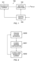
- FIG. 1 is a schematic diagram of a voltage reference circuit 100 in accordance with an embodiment of the disclosure.
- the voltage reference circuit 100 includes a source of current 101.
- the source of current 101 is connected to a switched-capacitor arrangement 102.
- the switched capacitor arrangement 102 includes two or more capacitors, connected together by a plurality of switches.
- the switched capacitor arrangement 102 is configured to share charge amongst the capacitors by controlling the switches.
- the source of current 101 is configured to charge one or more of the capacitors of the switched capacitors, depending on the arrangement of the switches.
- the source of current 101 may be a reference buffer, as will be described in more detail below.
- Suitable reference buffers include operational amplifiers, and specifically operational transconductance amplifiers (OTAs).
- the switched capacitor arrangement 102 provides a voltage reference V REFOUT at an output of the circuit 100.
- the output of the circuit 100 is coupled to a further circuit or device requiring a voltage reference.
- this further circuit is a successive approximation register (SAR) ADC.
- the switched capacitor arrangement 102 is configured to arrange the switches in order to provide an appropriate voltage at V REFOUT .
- the operation of the circuit 100 is dependent upon the circuit to which the voltage reference is being provided.
- the circuit 100 includes a control module 103.
- the control module 103 receives control information from the ADC.
- the control information includes the current phase of operation of the ADC, comprising whether the ADC is in a conversion or acquisition phase. Furthermore, the control information may include details of the ADC's previous input, as will be described in more detail below.
- the control module 103 is connected to, and configured to control, the switched capacitor arrangement 102 and optionally to the source of current 101.
- the control module 103 is configured to control the circuit 100 depending on the phase of operation of the circuit to which the voltage reference is being provided. These phases are related to conversion and acquisition phases of the ADC.
- the control module 103 controls the source of current 101 and the switch capacitor arrangement 102 so that in a first phase (S200), the switched capacitor arrangement 102 provides a voltage reference at the circuit output. This is the conversion phase of an ADC.
- the control module controls the switch capacitor arrangement such that it enters a charge-sharing configuration, to share charge amongst the capacitors of the switched capacitor arrangement 102. This is in a first part of an acquisition phase of the ADC.
- control module 103 controls the source of current 101 and the switched capacitor arrangement 102 such that the source of current charges at least one capacitor of the switched capacitor arrangement. This is a second part of the acquisition phase of the ADC. Finally, the circuit returns to the first phase of operation.
- control module is omitted for clarity. However, it is assumed that the switches are controlled by an appropriate control module or logic.
- FIG 3 is a circuit diagram of the voltage reference circuit 100 showing further details not shown in Figure 1 .
- the control module is omitted for clarity. However, it is assumed that the switches are controlled by an appropriate control module or logic.
- the voltage reference circuit 100 includes the source of current 101.
- the source of current may be a reference buffer, however other types of source of current may be used.
- the output of the source of current 101 is provided to the rest of the voltage reference circuit 100, as will be described in more detail below.
- the voltage reference circuit 100 includes the switched capacitor arrangement 102.
- the switched capacitor arrangement 102 is coupled to an output of the source of current 101.
- the source of current 101 is configured to provide current to the switched capacitor arrangement 102, in order to charge one or more capacitors which form part of the switched capacitor arrangement 102.
- the switched capacitor arrangement 102 includes a battery capacitor C BAT .
- the purpose of the battery capacitor C BAT is to store charge during the conversion phase of an analog-to-digital converter to which the voltage reference circuit 100 is connected.
- the switched capacitor arrangement 102 also includes a reservoir capacitor C RES .
- the reservoir capacitor C RES is for providing a reference voltage to a circuit to which the voltage reference circuit 100 is connected.
- the circuit is an analog-to-digital converter (ADC), such as a SAR ADC.
- ADC analog-to-digital converter
- the switched capacitor arrangement 102 also includes a plurality of switches 104A to 104D.
- An output of the source of current 101 is connected to a first switch 104A.
- the battery capacitor C BAT is connected between ground and a second switch 104B.
- the first switch 104A is also connected to the second switch 104B.
- the reservoir capacitor C RES is connected between ground and a third switch 104C.
- Switch 104C is also connected to the first switch 104A and the second switch 104B.
- a fourth switch 104D is also connected to the reservoir capacitor C RES and to an output V REFOUT of the circuit 100.
- the combination of switches 104A to 104D enables various combinations of the capacitors of the switched capacitor arrangement 102 to be connected to the output of the source of current 101, to other capacitors in the arrangement, and to the output of the circuit V REFOUT .
- FIG. 3 is a flow chart showing the method of operation of the voltage reference circuit 100 shown in Figure 3 .
- the operation begins when the ADC is operating in a conversion phase (S300).
- the voltage reference circuit 100 is required to provide the ADC with a voltage reference.
- the reservoir capacitor C RES must provide a reference voltage to the output V REFOUT . Accordingly, during the conversion phase C RES is disconnected from the source of current 101 and the remainder of the switched capacitor arrangement 102 by opening switch 104C.
- switch 104D is closed in order to connect the reservoir capacitor C RES to V REFOUT and the ADC (S301). This is shown in the circuit diagram shown in Figure 3 .
- the charge on the reservoir capacitor C RES is gradually depleted.
- the amount of charge depleted by the ADC converter will depend upon which bit is currently being considered by the SAR ADC. As such, the degree to which C RES is depleted is input-dependent.
- the source of current 101 is used to charge the battery capacitor C BAT (S302).
- switches 104A and 104B are closed.
- the conversion phase may be regarded as the first phase of operation of the voltage reference circuit 100.
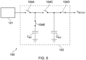
- FIG. 5 shows the configuration of the voltage reference circuit 100 at the end of the conversion phase.
- C RES remains disconnected from C BAT and from the source of current 101.
- C BAT is also disconnected from the source of current 101 by opening switch 104A (S303).
- the charge on C RES has been depleted to a degree during the conversion phase of the ADC.
- the capacitor battery C BAT is sufficiently or fully charged in preparation for boosting the charge on the reservoir capacitor C RES .
- the next phase of operation is when the ADC enters its acquisition phase.
- the first part of the acquisition phase may be regarded as a second phase of operation of the voltage reference circuit 100.
- the voltage reference circuit 100 is no longer required to supply a voltage reference to the ADC. As such, the circuit replenishes the charge on C RES during this period.
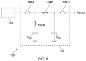
- FIG. 6 shows the configuration of the voltage reference circuit 100 at the beginning of the ADC's acquisition phase.
- the battery capacitor C BAT is connected to the reservoir capacitor C RES in order to boost the charge on the reservoir capacitor C RES .
- the purpose of this is to reduce the load on the source of current 101 during the remainder of the acquisition phase.
- the output V REFOUT is disconnected from the ADC by opening switch 104D (S304).
- Switch 104A remains open, and switch 104C is closed in order to connect the reservoir capacitor C RES to the battery capacitor C BAT (S305).
- C BAT and C RES therefore enter a charge sharing arrangement.
- the charge on C BAT is much greater than the charge on C RES , charge flows onto capacitor C RES .
- the voltage on C RES is much closer to the required V REFOUT , meaning that the source of current 101 does not have much work to do to top up the charge on C RES .
- the circuit enters a third phase of operation which is the second part of the acquisition phase of the ADC. This is shown in Figure 7 .
- C RES is disconnected from C BAT by opening switch 104B (S306).
- Switch 104A is closed to connect C RES directly to the output of the source of current 101 (S307).
- the source of current 101 now has to replenish very little charge on C RES .
- the process then returns to the conversion phase and the arrangement shown in Figure 3 .
- the switched capacitor arrangement 102 provides a boost to the reservoir capacitor C RES at the beginning of the acquisition phase. This reduces the burden on the source of current 101, and enables C RES to be charged more quickly that might be possible with the source of current 101 alone.
- FIG. 8 is a circuit diagram of a voltage reference circuit 400 in accordance with an embodiment of this disclosure.
- the voltage reference circuit 400 includes a reference buffer 401.
- the reference buffer 401 includes an amplifier 402 which may be a transistor-level single-stage operational transconductance amplifier (OTA).
- OTA operational transconductance amplifier
- the output of the amplifier 402 is coupled to the inverting input 403 of the amplifier in order to provide negative feedback.
- a band gap voltage source 404 is connected between ground and the non-inverting input 405 of the amplifier 402.
- the amplifier 402 acts as a unity gain buffer.
- the output of the amplifier 402 acts as a source of current which is provided to the rest of the voltage reference circuit 400 in order to provide a reference voltage, as will be described in more detail below.
- the circuit 400 also includes a stabilisation capacitor C STABIL which is provided to stabilise the amplifier 402 when the other capacitors are disconnected from the amplifier.
- C STABIL is connected between ground and an output of the amplifier 402.
- the voltage reference circuit 400 includes a switched capacitor arrangement 406.
- the switched capacitor arrangement 406 is coupled to an output of the reference buffer 401.
- the reference buffer 401 is configured to provide current to the switched capacitor arrangement 406, in order to charge one or more capacitors which form part of the switched capacitor arrangement 406.
- the switched capacitor arrangement 406 includes a battery capacitor C BAT .
- the battery capacitor C BAT may be composed of a plurality of sub-capacitors.
- the battery capacitor C BAT includes sub-capacitors Cx and C Y .
- the battery capacitor is composed of two sub-capacitors in a configuration that enables the value of C BAT to be changed. This will be described in further detail below.
- the purpose of the battery capacitor C BAT is to store charge during the conversion phase of an analog-to-digital converter to which the voltage reference circuit 400 is connected.
- the switched capacitor arrangement 406 also includes a reservoir capacitor C RES .
- the reservoir capacitor C RES is for providing a reference voltage to a circuit to which the voltage reference circuit 400 is connected.
- the circuit is a SAR analog-to-digital converter (ADC).
- the switched capacitor arrangement 406 also includes a plurality of switches 407A to 407G.
- Sub-capacitor Cx is connected between ground and a first switch 407A.
- the first switch 407A is also connected to an output of the reference buffer 401.
- the sub-capacitor C Y is connected to a second switch 407B.
- Second switch 407B is also connected to ground.
- Sub-capacitor C Y is also connected to a third switch 407C.
- Third switch 407C is also connected to an output of the reference buffer 401 and to the first switch 407A.
- a fourth switch 407D is connected between the sub-capacitors Cx and C Y .
- a fifth switch 407E is also connected between C RES and the sub-capacitor C Y .
- sixth switch 407F is connected between an output of the reference buffer 401 and the reservoir capacitor C RES .
- the reservoir capacitor C RES is connected between ground and the output reference voltage V REFOUT via a seventh switch 407G.
- switches 407A to 407G enables various combinations of the capacitors of the switched capacitor arrangement 406 to be connected to the output of the reference buffer 401, to other capacitors in the arrangement, and to the output of the circuit V REFOUT .
- the switches associated with the battery capacitor C BAT enable the sub-capacitors Cx and C Y to be connected together in series or in parallel, thereby enabling different voltages to be supplied to the reservoir capacitor C RES .
- FIG. 9 is a flow chart showing the method of operation of the voltage reference circuit 400 shown in Figure 8 .
- the operation begins when the ADC is operating in a conversion phase (S500).
- the voltage reference circuit is required to provide the ADC with a voltage reference.
- the reservoir capacitor C RES must provide a reference voltage to the output V REFOUT .
- switch 407G is closed in order to connect the reservoir capacitor C RES .
- the reference buffer 401 is used to charge the battery capacitor C BAT (S502). As such, switches 407A, 407B and 407C are closed, and switch 407D is open. During the conversion phase the reference buffer 401 charges the sub-capacitors C X and C Y .
- the conversion phase may be regarded as the first phase of operation of the voltage reference circuit 400.
- FIG 10 shows the configuration of the voltage reference circuit 400 at the end of the conversion phase.
- C RES remains disconnected from C BAT and from the reference buffer 400.
- C BAT is also disconnected from the reference buffer 401 by opening switches 407A and 407C (S503).
- the charge on C RES has been depleted to a degree during the conversion phase of the ADC.
- the sub-capacitors C X and C Y of the capacitor battery C BAT are sufficiently or fully charged in preparation for boosting the charge on the reservoir capacitor C RES .
- the next phase of operation is when the ADC enters its acquisition phase.
- the first part of the acquisition phase may be regarded as a second phase of operation of the voltage reference circuit 400.
- the voltage reference circuit is no longer required to supply a voltage reference to the ADC. As such, the circuit replenishes the charge on C RES during this period.
- FIG 11 shows the configuration of the voltage reference circuit 400 at the beginning of the ADC's acquisition phase.
- the battery capacitor C BAT is connected to the reservoir capacitor C RES in order to boost the charge on the reservoir capacitor C RES .
- the purpose of this is to reduce the load on the reference buffer 401 during the remainder of the acquisition phase.
- the output V REFOUT is disconnected from the ADC by opening switch 407G (S504).
- Switch 407F remains open, and switch 407E is closed in order to connect the reservoir capacitor C RES to the battery capacitor C BAT (S505).
- the sub-capacitors C X and C Y of the battery capacitor C BAT are, in this example, arranged in series.
- switch 407A is opened, switch 407B is opened, switch 407D is closed, and switch 407C is opened.
- C BAT and C RES therefore enter a charge sharing arrangement.
- charge on C BAT is much greater than the charge on C RES , charge flows onto capacitor C RES .
- the voltage on C RES is much closer to the required V REFOUT , meaning that the reference buffer 401 does not have much work to do to top up the charge on C RES .
- sub-capacitors C X and C Y may be controlled digitally to vary their individual values.
- the value of C BAT may be digitally controlled.
- the values of Cx and C Y can be a function of the ADC's output from the previous conversion.
- the charge supplied by C BAT can be a function of the previous input of the ADC.
- the amount of charge lost in C RES due to the ADC's conversion is a function of the input of the ADC, this reduces the input-dependence of the current demand from the reference buffer 401.
- the circuit enters a third phase of operation which is the second part of the acquisition phase of the ADC. This is shown in Figure 12 .
- Switch 407F is closed to connect C RES directly to the output of the reference buffer 401 (S506).
- the reference buffer 401 now has to replenish very little charge on C RES , as the input-dependent reference current has been supplied by C BAT .
- the process then returns to the conversion phase and the arrangement shown in Figure 8 .
- the switched capacitor arrangement 406 provides slew assist to the amplifier 402 of the reference buffer 401.
- the rate at which the reservoir capacitor C RES is recharged is much greater than the slew rate of the amplifier 402 of the buffer 401.
- the reservoir capacitor C RES has a value of 80pF and the acquisition time was 30ns.
- the reference voltage provided by the band gap reference 404 is 2.2v.
- the switches have a resistance of 10 ⁇ to 100 ⁇ .
- Figure 13 is a timing chart for the different phases of operation described above in connection with the voltage reference circuit 400.
- the upper chart 600 shows the first part of the acquisition phase when charge-sharing occurs between C RES and C BAT . As can be seen, this boost portion 601 of the operation of the circuit lasts around 2ns.
- the middle chart 602 shows the second part 603 of the acquisition phase, when C RES is charged by the reference buffer 401. As can be seen, this portion of the operation lasts for around 28ns.
- the lower chart 604 shows the conversion phase 605 of the ADC. As can be seen, this lasts for around 30ns.
- Figure 14 shows the voltage across the reservoir capacitor C RES during operation of the voltage reference circuit 400.
- the upper chart 700 shows voltage across the reservoir capacitor during first part of acquisition phase.
- the lower chart 701 shows the first part of the acquisition phase.
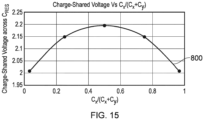
- Figure 15 shows the charge-shared voltage 800 across C RES based on various different values of C X and C Y .
- Figure 15 shows variation in the fraction C x /(C x +C y ) from 1/32 to 31/32 in five steps.
- the profile of the charge drawn by the reservoir capacitor is very similar to the ADC's reference charge consumption with reference to its input voltage.
- the maximum charge is drawn near the inputs corresponding to mid-codes, and the curve is symmetric about the mid-codes. Therefore, the battery capacitor can be configured such that C x /(C x +C y ) is close to 0.5 when the previous ADC input is close to the mid-codes.
- C x /(C x +C y ) is close to 0 or 1 when the previous ADC input is close to the end-codes.
- most of the input-dependent reference charge required from the reference buffer may be eliminated (or significantly reduced). This will significantly reduce the design complexity of the reference buffer.
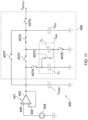
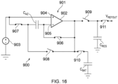
- FIG. 16 shows a voltage reference circuit 900 in accordance with a further embodiment of the disclosure.
- the voltage reference circuit 900 includes a reference buffer 901.
- the reference buffer 901 includes an amplifier 902 which may be an auto-zeroed load-stabilized two-stage amplifier.
- the inventors of the present disclosure have appreciated that by disconnecting the voltage reference circuit from the ADC, during the acquisition phase, the amplifier of the reference buffer may be auto-zeroed. In this particular case, the use of an auto-zeroed load-stabilized two-stage amplifier improves the circuit's immunity to 1/f noise.
- a band gap voltage source 903 is connected to the non-inverting input 904 of the amplifier 902. Other types of voltage source may be used.
- the output of the amplifier 902 provides negative feedback to the inverting input 905 of amplifier 902.
- Switch 906 is provided in the feedback loop.
- An auto-zero capacitor C AZ is coupled between the inverting input of the amplifier 905 and the band gap voltage source 903.
- a switch 907 is provided between C AZ and the band gap voltage source 903.
- the output of the amplifier 902 is also connected to the switch 907 and the capacitor C AZ via switch 908.
- a reservoir capacitor C RES is connected to an output of the amplifier 902 via switch 909. C RES is also connected to ground and to the output of the circuit V REFOUT via switch 911.
- a battery capacitor C BAT is also coupled to the output of amplifier 902 via switch 910.
- FIG. 16 shows the configuration of the voltage reference circuit 900 during a first phase of operation.
- the first phase of operation is while an ADC to which the circuit is connected is in a conversion phase (S1000).
- the amplifier 902 is auto-zeroed by closing switch 907 and 906 in order to store the input-offset voltage and 1/f noise on capacitor C AZ (S1001).
- Switch 909 is open so that the reservoir capacitor C RES is not connected to the output of the amplifier 902. Instead, the reservoir capacitor is connected to V REFOUT by closing switch 911 (S1002).
- Switch 908 is open and switch 910 is closed.
- C BAT acts as a stabilization capacitor which gets charged close to the reference voltage of the band gap voltage reference 903 (S1003).
- FIG 18 shows the voltage reference circuit 900 at the end of the first phase of operation. This is at the end of the ADC's conversion phase. In this phase, switches 907 and 906 are opened and switch 908 is closed. Here, the amplifier 902 transitions from its auto-zeroed state to normal (or amplification) operation (S1004). The C AZ capacitor cancels the input offset and 1/f noise and remains connected between the amplifier's output and its inverting input 905. There is no change in state for C BAT and C RES during this step.
- FIG 19 shows the configuration of the voltage reference circuit 900 during the first part of the acquisition phase. This may be regarded as the second phase of operation.
- switch 909 is closed at the same time as C RES is disconnected from the ADC by opening switch 911.
- C RES is connected to the reference buffer 901 and also to C BAT (S1005).
- C BAT S1005
- Charge-sharing occurs between C RES and C BAT .
- the value of C BAT is the same as the value of C RES .
- the duration of this step is so small that the amplifier does not get time to slew the load seen on its output.
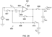
- FIG 20 shows the voltage reference circuit 900 in the third phase of operation, which is the second part of the acquisition phase.
- switch 910 is open to disconnect C BAT from the reference buffer 901 and from C RES (S1006).
- Switch 909 remains closed so that C RES remains connected to the output of the amplifier 902.
- C RES gets charged during this phase by the reference buffer to the reference voltage of the band gap voltage source (S1007).
- the amplifier goes back to the configuration shown in Figure 16 .
- Figure 21 is a chart 1100 showing the transient waveform of voltage across the reservoir capacitor for this embodiment.
- C BAT provides slew assist in order to provide the reservoir capacitor with around 50% of its charge.
- the reference buffer charges C RES up to the reference voltage.
- the reservoir capacitor C RES recovers around 50% of its charge within 1ns.
- the amplifier 902 then replenishes the remaining charge in the rest of the acquisition time.
- An advantage of the above-described examples is that, because the reservoir capacitor is provided with a charge boost, the amount of charge required from the reference buffer is reduced.
- the input-dependent reference current can be reduced by controlling the charge available from the battery capacitor C BAT . This may be controlled as a function of the ADC's output data based on the previous conversion. Additionally, as the demand on the reference buffer 401, 901 is reduced, the corresponding ringing on the supply of the reference buffer is also reduced in the acquisition phase, making the overall system quieter. Furthermore, by charge-sharing between the reservoir capacitor and the battery capacitor, the slew rate and unity gain frequency (UGF) requirements on the amplifier are relaxed, thereby reducing power consumption and making the reference buffer 401, 901 easier to design.
- UPF unity gain frequency
- source of current refers to an element that provides current to the capacitors of the switch-capacitor arrangement.
- a source of current may provide current at different values, depending on the load.
Landscapes
- Engineering & Computer Science (AREA)
- Power Engineering (AREA)
- Theoretical Computer Science (AREA)
- Analogue/Digital Conversion (AREA)
Description
- The present disclosure relates to a voltage reference circuit configured for providing a reference voltage to a successive approximation register, SAR, analog-to-digital converter circuit and a method for providing a voltage reference to a successive approximation register, SAR, analog-to-digital converter circuit.
- Analog-to-Digital Converters (ADCs) typically convert an analog input voltage into a digital output code. In order to do this, most ADCs compare the input voltage to a reference voltage using a device such as a comparator. A 1-bit ADC uses a single comparator and compares the input voltage to the reference voltage. The ADC outputs a "1" if the input is higher than the reference voltage, and a "0" if the input voltage is lower than the reference voltage. Multi-bit ADCs are more complex, and generate multi-bit output codes. One such multi-bit ADC is a successive approximation register (SAR) ADC. A SAR ADC operates by generating a digital approximation of the analog input voltage. It does this bit-by-bit, starting with the highest bit (the most significant bit, or MSB) and moving down to the lowest bit (the least significant bit, or LSB). To do this, it uses a digital-to-analog converter (DAC) which generates an analog voltage to compare with the input voltage using a comparator. It is common for SAR ADCs to use capacitive DACs, however, other types of DAC are used in some SAR ADCs. The DAC requires a reference voltage in order to generate a suitable analog voltage for comparison with the input voltage.
- The voltage reference is typically supplied by a voltage reference circuit. In the case of SAR ADCs, the voltage reference circuit provides charge to the ADC using one or more capacitors. For example, a typical voltage reference circuit for a SAR ADC includes a reference buffer connected to a decoupling capacitor. The reference buffer may or may not be provided on the same chip as the ADC.
- However, the decoupling capacitor is required to be large (in the order of 10uF), and is therefore provided off-chip. The decoupling capacitor is required to be large because it needs to provide enough charge for a complete conversion, which includes multiple bit trials. The capacitor needs to be large enough such that the accuracy of later bit trials are not degraded as the charge of the decoupling capacitor is reduced. However, a large off-chip capacitor is expensive and utilises valuable area on the printed circuit board (PCB). Furthermore, a large decoupling capacitor means that the output impedance of the circuit is required to be low, which in turn makes design of the reference buffer challenging.
- In addition to the above, a key requirement of the voltage reference circuit is that reference value does not drop too much as the ADC draws charge during a conversion phase. The reference buffer needs to charge the off-chip capacitor back to the reference charge before the next conversion phase starts. The greater the drop in charge, the more work the reference buffer has to do.
-
US 2007/046523 A1 discloses a reference voltage generating circuit which includes: a first capacitor; a second capacitor; a reference voltage sampling capacitor; a first switch for alternatively coupling the second capacitor to a predetermined voltage to allow the second capacitor to sample the predetermined voltage; a second switch for alternatively coupling the second capacitor to the first capacitor to allow the second capacitor to redistribute charges with the first capacitor in order to generate the reference voltage; and a third switch for alternatively coupling the first capacitor to the reference voltage sampling capacitor to allow the reference voltage sampling capacitor to redistribute charges with the first capacitor in order to output the reference voltage. -
WO 2008/131185 A1 discloses a digital to analog converter reference circuit, comprising a capacitor connected to a current source, a positive terminal of the capacitor connected to a first switch, the first switch electrically connecting the positive terminal of the capacitor to a positive input terminal of a DAC circuit, a negative terminal of the capacitor connected to a second switch, the second switch electrically connecting the negative terminal of the capacitor to a negative input terminal of the DAC circuit. Further, it discloses a method for converting digital code to an analog signal, comprising charging a reservoir capacitor to a reference voltage level, transferring stored charge from the reservoir capacitor to DAC feedback capacitors, and transferring the stored charge from the DAC feedback capacitors to DAC output terminals. -
US2014/253223 A1 discloses a signal processing apparatus that includes a circuit in which a signal processing function is performed during a first time period, the signal processing apparatus including or being associated with a switch or a filter in a power supply to the signal processing apparatus so as to disconnect the signal processing apparatus from the power supply or to filter the power supply during a second time period that is coincident with at least part of the first time period. - The present disclosure relates to a voltage reference circuit and a method of providing a voltage reference. The voltage reference circuit uses a switched capacitor arrangement to move charge between capacitors during different phases of operation of the circuit to which the voltage reference is being provided. The circuit being provided with a voltage reference is an analog-to-digital converter (ADC). A reservoir capacitor is used to supply the reference voltage. During a phase in which no voltage reference is required, charge is shared between the capacitors of the switched capacitor arrangement, in order to boost the charge on the reservoir capacitor. After charge sharing, the reservoir capacitor is topped up with an output from a reference buffer. The reservoir capacitor may then be used again in the next conversion phase.
- In a first aspect, the present disclosure provides a voltage reference circuit as defined in
claim 1. - In a second aspect, the present disclosure provides a method of providing a reference voltage as defined in claim 7.
- In a further embodiment, a circuit according to any preceding aspect, wherein the switched capacitor arrangement further comprises: a first switch, connected between the battery capacitor and the output of the reference buffer; and wherein the switched capacitor arrangement is further configured to: close the first switch at the beginning of the conversion phase of the SAR ADC; and keep the first switch open during the second part of the acquisition phase of the SAR ADC.
- In a further embodiment, a circuit according to any preceding aspect, wherein the switched capacitor arrangement further comprises: a second switch, connected between the reservoir capacitor and the reference buffer; and wherein the switch capacitor arrangement is further configured to: open the second switch at the beginning of the conversion phase of the SAR ADC; keep the second switch closed during the second part of the acquisition phase of of the SAR ADC.
- In a further embodiment, a circuit according to any preceding aspect, wherein the switched capacitor arrangement further comprises: a third switch, connected between the reservoir capacitor and the battery capacitor; and wherein the switch capacitor arrangement is further configured to: open the third switch at the beginning of the conversion phase of the SAR ADC; close the third switch at the beginning of the first part of the acquisition phase of the SAR ADC; and open the third switch at the beginning of the second part of the acquisition phase of the SAR ADC.
- Further aspects and features of the disclosure may be found in the appended claims.
- The present disclosure will now be described, by way of example only, and with reference to the accompanying drawings, in which:
-
Figure 1 is a schematic diagram of a circuit in accordance with an embodiment of the disclosure; -
Figure 2 is a flow chart showing a method of operation of the circuit ofFigure 1 ; -
Figure 3 is a schematic diagram of a circuit in a first configuration, in accordance with a further embodiment of the disclosure; -
Figure 4 is a flow chart showing a method of operation of the circuit ofFigure 3 ; -
Figure 5 is a schematic diagram of the circuit ofFigure 3 in a second configuration; -
Figure 6 is a schematic diagram of the circuit ofFigure 3 in a third configuration; -
Figure 7 is a schematic diagram of the circuit ofFigure 3 in a fourth configuration; -
Figure 8 is a schematic diagram of a circuit in a first configuration, in accordance with a further embodiment of the disclosure; -
Figure 9 is a flow chart showing a method of operation of the circuit ofFigure 8 ; -
Figure 10 is a schematic diagram of the circuit ofFigure 8 in a second configuration; -
Figure 11 is a schematic diagram of the circuit ofFigure 8 in a third configuration; -
Figure 12 is a schematic diagram of the circuit ofFigure 8 in a fourth configuration; -
Figure 13 shows three charts showing the phases of operation of the circuit shown inFigure 8 ; -
Figure 14 shows two charts showing the voltage across a reservoir capacitor of the circuit ofFigure 8 ; -
Figure 15 shows a chart showing the voltage across the reservoir capacitor ofFigure 8 at the end of charge sharing; -
Figure 16 is a schematic diagram of a circuit in a first configuration, in accordance with a further embodiment of the disclosure; -
Figure 17 is a flow chart showing a method of operation of the circuit ofFigure 16 ; -
Figure 18 is a schematic diagram of the circuit ofFigure 16 in a second configuration; -
Figure 19 is a schematic diagram of the circuit ofFigure 16 in a third configuration; -
Figure 20 is a schematic diagram of the circuit ofFigure 16 in a fourth configuration; and -
Figure 21 is a chart showing the transient waveform of voltage across a reservoir capacitor of the circuit shown inFigure 16 during an ADC's acquisition phase. - The present disclosure provides a voltage reference circuit which includes a switched capacitor arrangement. The circuit charges different capacitors during different phases of operation, and utilising charge-sharing to boost the charge on the reservoir capacitor. This arrangement removes the requirement for a large, off-chip capacitor, and reduces the load on the reference buffer, making buffer design more straight-forward.
- The circuit is particularly suitable for providing an ADC with a reference voltage. As such, the voltage reference circuit is operated with reference to the conversion and acquisition phases of the ADC. The voltage reference circuit includes an output, or reservoir capacitor, which provides the reference voltage to the ADC. At the beginning of the conversation phase, the reservoir capacitor is fully or sufficiently charged. The reservoir capacitor provides the required reference voltage, and the charge on the reservoir capacitor is gradually depleted during the conversion phase. During this same time, another capacitor of the switched capacitor arrangement is gradually charged by a source of current, such as a reference buffer. This capacitor is referred to as a battery capacitor. At the end of the conversion phase, the battery capacitor is fully or sufficiently charged.
- As soon as the conversion phase is over, the ADC begins the acquisition phase. At the beginning of the acquisition phase, the reservoir capacitor is disconnected from the ADC, and connected to the battery capacitor. Charge sharing then occurs between the capacitors, such that the charge on the reservoir capacitor is boosted by the battery capacitor. Charge sharing occurs for a short duration at the beginning of the acquisition phase. The duration of this phase should be long enough for charge sharing to be complete, or for sufficient charge to transfer to the reservoir capacitor.
- After charging sharing is complete, the reservoir capacitor is disconnected from the battery capacitor and the remaining charge for the reservoir capacitor is provided by the reference buffer. As the amount of charge required is typically much less than half of the value of the reservoir capacitor, the reference buffer can top up the reservoir capacitor during the rest of the acquisition phase.
- The charge-sharing arrangement effectively provides slew-assist to the amplifier of the reference buffer, by charging the reservoir capacitor at a rate not possible using the reference buffer alone. Owing to ADC redundancy, the value of the reservoir capacitor can be small enough that it can be provided on-chip. Furthermore, the design of the reference buffer is more straight-forward, owing to the reduced charging requirements.
-
Figure 1 is a schematic diagram of avoltage reference circuit 100 in accordance with an embodiment of the disclosure. Thevoltage reference circuit 100 includes a source of current 101. The source of current 101 is connected to a switched-capacitor arrangement 102. The switchedcapacitor arrangement 102 includes two or more capacitors, connected together by a plurality of switches. The switchedcapacitor arrangement 102 is configured to share charge amongst the capacitors by controlling the switches. The source of current 101 is configured to charge one or more of the capacitors of the switched capacitors, depending on the arrangement of the switches. - The source of current 101 may be a reference buffer, as will be described in more detail below. Suitable reference buffers include operational amplifiers, and specifically operational transconductance amplifiers (OTAs).
- The switched
capacitor arrangement 102 provides a voltage reference VREFOUT at an output of thecircuit 100. The output of thecircuit 100 is coupled to a further circuit or device requiring a voltage reference. According to the invention, this further circuit is a successive approximation register (SAR) ADC. The switchedcapacitor arrangement 102 is configured to arrange the switches in order to provide an appropriate voltage at VREFOUT. - The operation of the
circuit 100 is dependent upon the circuit to which the voltage reference is being provided. As such, thecircuit 100 includes acontrol module 103. Thecontrol module 103 receives control information from the ADC. The control information includes the current phase of operation of the ADC, comprising whether the ADC is in a conversion or acquisition phase. Furthermore, the control information may include details of the ADC's previous input, as will be described in more detail below. Thecontrol module 103 is connected to, and configured to control, the switchedcapacitor arrangement 102 and optionally to the source of current 101. - The method of operation of the circuit shown in
Figure 1 will now be described with reference toFigure 2 . Thecontrol module 103 is configured to control thecircuit 100 depending on the phase of operation of the circuit to which the voltage reference is being provided. These phases are related to conversion and acquisition phases of the ADC. Thecontrol module 103 controls the source of current 101 and theswitch capacitor arrangement 102 so that in a first phase (S200), the switchedcapacitor arrangement 102 provides a voltage reference at the circuit output. This is the conversion phase of an ADC. In a second phase (S201), the control module controls the switch capacitor arrangement such that it enters a charge-sharing configuration, to share charge amongst the capacitors of the switchedcapacitor arrangement 102. This is in a first part of an acquisition phase of the ADC. In a third phase of operation (S202), thecontrol module 103 controls the source of current 101 and the switchedcapacitor arrangement 102 such that the source of current charges at least one capacitor of the switched capacitor arrangement. This is a second part of the acquisition phase of the ADC. Finally, the circuit returns to the first phase of operation. - In the following embodiments, the control module is omitted for clarity. However, it is assumed that the switches are controlled by an appropriate control module or logic.
-
Figure 3 is a circuit diagram of thevoltage reference circuit 100 showing further details not shown inFigure 1 . The control module is omitted for clarity. However, it is assumed that the switches are controlled by an appropriate control module or logic. Thevoltage reference circuit 100 includes the source of current 101. The source of current may be a reference buffer, however other types of source of current may be used. The output of the source of current 101 is provided to the rest of thevoltage reference circuit 100, as will be described in more detail below. - The
voltage reference circuit 100 includes the switchedcapacitor arrangement 102. The switchedcapacitor arrangement 102 is coupled to an output of the source of current 101. The source of current 101 is configured to provide current to the switchedcapacitor arrangement 102, in order to charge one or more capacitors which form part of the switchedcapacitor arrangement 102. The switchedcapacitor arrangement 102 includes a battery capacitor CBAT. The purpose of the battery capacitor CBAT is to store charge during the conversion phase of an analog-to-digital converter to which thevoltage reference circuit 100 is connected. - The switched
capacitor arrangement 102 also includes a reservoir capacitor CRES. The reservoir capacitor CRES is for providing a reference voltage to a circuit to which thevoltage reference circuit 100 is connected. The circuit is an analog-to-digital converter (ADC), such as a SAR ADC. The switchedcapacitor arrangement 102 also includes a plurality ofswitches 104A to 104D. An output of the source of current 101 is connected to afirst switch 104A. The battery capacitor CBAT is connected between ground and asecond switch 104B. Thefirst switch 104A is also connected to thesecond switch 104B. The reservoir capacitor CRES is connected between ground and athird switch 104C.Switch 104C is also connected to thefirst switch 104A and thesecond switch 104B. Afourth switch 104D is also connected to the reservoir capacitor CRES and to an output VREFOUT of thecircuit 100. - The combination of
switches 104A to 104D enables various combinations of the capacitors of the switchedcapacitor arrangement 102 to be connected to the output of the source of current 101, to other capacitors in the arrangement, and to the output of the circuit VREFOUT. - The operation of the circuit shown in
Figure 3 will now be described with reference to the phases of operation of a SAR analog-to-digital converter (ADC).Figure 4 is a flow chart showing the method of operation of thevoltage reference circuit 100 shown inFigure 3 . The operation begins when the ADC is operating in a conversion phase (S300). During the conversion phase, thevoltage reference circuit 100 is required to provide the ADC with a voltage reference. As such, during the conversion phase the reservoir capacitor CRES must provide a reference voltage to the output VREFOUT. Accordingly, during the conversion phase CRES is disconnected from the source of current 101 and the remainder of the switchedcapacitor arrangement 102 by openingswitch 104C. Additionally, switch 104D is closed in order to connect the reservoir capacitor CRES to VREFOUT and the ADC (S301). This is shown in the circuit diagram shown inFigure 3 . During this phase of operation, the charge on the reservoir capacitor CRES is gradually depleted. The amount of charge depleted by the ADC converter will depend upon which bit is currently being considered by the SAR ADC. As such, the degree to which CRES is depleted is input-dependent. During the conversion phase, the source of current 101 is used to charge the battery capacitor CBAT (S302). As such, switches 104A and 104B are closed. The conversion phase may be regarded as the first phase of operation of thevoltage reference circuit 100. -
Figure 5 shows the configuration of thevoltage reference circuit 100 at the end of the conversion phase. At this point, CRES remains disconnected from CBAT and from the source of current 101. However, CBAT is also disconnected from the source of current 101 by openingswitch 104A (S303). At this stage of operation, the charge on CRES has been depleted to a degree during the conversion phase of the ADC. The capacitor battery CBAT is sufficiently or fully charged in preparation for boosting the charge on the reservoir capacitor CRES. - The next phase of operation is when the ADC enters its acquisition phase. The first part of the acquisition phase may be regarded as a second phase of operation of the
voltage reference circuit 100. During the acquisition phase, thevoltage reference circuit 100 is no longer required to supply a voltage reference to the ADC. As such, the circuit replenishes the charge on CRES during this period. -
Figure 6 shows the configuration of thevoltage reference circuit 100 at the beginning of the ADC's acquisition phase. During this phase, the battery capacitor CBAT is connected to the reservoir capacitor CRES in order to boost the charge on the reservoir capacitor CRES. The purpose of this is to reduce the load on the source of current 101 during the remainder of the acquisition phase. As such, during this phase of operation the output VREFOUT is disconnected from the ADC by openingswitch 104D (S304).Switch 104A remains open, andswitch 104C is closed in order to connect the reservoir capacitor CRES to the battery capacitor CBAT (S305). CBAT and CRES therefore enter a charge sharing arrangement. As the charge on CBAT is much greater than the charge on CRES, charge flows onto capacitor CRES. At the end of the first part of the acquisition phase, the voltage on CRES is much closer to the required VREFOUT, meaning that the source of current 101 does not have much work to do to top up the charge on CRES. - Once charge-sharing between CBAT and CRES is complete, the circuit enters a third phase of operation which is the second part of the acquisition phase of the ADC. This is shown in
Figure 7 . In this stage of the operation, CRES is disconnected from CBAT by openingswitch 104B (S306).Switch 104A is closed to connect CRES directly to the output of the source of current 101 (S307). The source of current 101 now has to replenish very little charge on CRES. The process then returns to the conversion phase and the arrangement shown inFigure 3 . - The switched
capacitor arrangement 102 provides a boost to the reservoir capacitor CRES at the beginning of the acquisition phase. This reduces the burden on the source of current 101, and enables CRES to be charged more quickly that might be possible with the source of current 101 alone. -
Figure 8 is a circuit diagram of avoltage reference circuit 400 in accordance with an embodiment of this disclosure. Thevoltage reference circuit 400 includes areference buffer 401. Thereference buffer 401 includes anamplifier 402 which may be a transistor-level single-stage operational transconductance amplifier (OTA). The output of theamplifier 402 is coupled to the invertinginput 403 of the amplifier in order to provide negative feedback. A bandgap voltage source 404 is connected between ground and thenon-inverting input 405 of theamplifier 402. As such, theamplifier 402 acts as a unity gain buffer. The output of theamplifier 402 acts as a source of current which is provided to the rest of thevoltage reference circuit 400 in order to provide a reference voltage, as will be described in more detail below. As an alternative to a band gap voltage source, other types of voltage source may be utilised. Thecircuit 400 also includes a stabilisation capacitor CSTABIL which is provided to stabilise theamplifier 402 when the other capacitors are disconnected from the amplifier. CSTABIL is connected between ground and an output of theamplifier 402. - The
voltage reference circuit 400 includes a switchedcapacitor arrangement 406. The switchedcapacitor arrangement 406 is coupled to an output of thereference buffer 401. Thereference buffer 401 is configured to provide current to the switchedcapacitor arrangement 406, in order to charge one or more capacitors which form part of the switchedcapacitor arrangement 406. - The switched
capacitor arrangement 406 includes a battery capacitor CBAT. The battery capacitor CBAT may be composed of a plurality of sub-capacitors. According to an embodiment, the battery capacitor CBAT includes sub-capacitors Cx and CY. The battery capacitor is composed of two sub-capacitors in a configuration that enables the value of CBAT to be changed. This will be described in further detail below. The purpose of the battery capacitor CBAT is to store charge during the conversion phase of an analog-to-digital converter to which thevoltage reference circuit 400 is connected. - The switched
capacitor arrangement 406 also includes a reservoir capacitor CRES. The reservoir capacitor CRES is for providing a reference voltage to a circuit to which thevoltage reference circuit 400 is connected. The circuit is a SAR analog-to-digital converter (ADC). The switchedcapacitor arrangement 406 also includes a plurality ofswitches 407A to 407G. Sub-capacitor Cx is connected between ground and afirst switch 407A. Thefirst switch 407A is also connected to an output of thereference buffer 401. The sub-capacitor CY is connected to asecond switch 407B.Second switch 407B is also connected to ground. Sub-capacitor CY is also connected to athird switch 407C.Third switch 407C is also connected to an output of thereference buffer 401 and to thefirst switch 407A. Afourth switch 407D is connected between the sub-capacitors Cx and CY. Afifth switch 407E is also connected between CRES and the sub-capacitor CY. Additionally,sixth switch 407F is connected between an output of thereference buffer 401 and the reservoir capacitor CRES. The reservoir capacitor CRES is connected between ground and the output reference voltage VREFOUT via aseventh switch 407G. - The combination of
switches 407A to 407G enables various combinations of the capacitors of the switchedcapacitor arrangement 406 to be connected to the output of thereference buffer 401, to other capacitors in the arrangement, and to the output of the circuit VREFOUT. In particular, the switches associated with the battery capacitor CBAT enable the sub-capacitors Cx and CY to be connected together in series or in parallel, thereby enabling different voltages to be supplied to the reservoir capacitor CRES. - The operation of the circuit shown in
Figure 8 will now be described with reference to the phases of operation of a SAR analog-to-digital converter (ADC).Figure 9 is a flow chart showing the method of operation of thevoltage reference circuit 400 shown inFigure 8 . The operation begins when the ADC is operating in a conversion phase (S500). During the conversion phase, the voltage reference circuit is required to provide the ADC with a voltage reference. As such, during the conversion phase the reservoir capacitor CRES must provide a reference voltage to the output VREFOUT. Accordingly, during the conversion phase CRES is disconnected from thereference buffer 401 and the remainder of the switchedcapacitor arrangement 406 by openingswitches switch 407G is closed in order to connect the reservoir capacitor CRES. This is shown in the circuit diagram shown inFigure 8 . During this phase of operation, the charge on the reservoir capacitor CRES is gradually depleted. The amount of charge depleted by the ADC will depend upon which bit is currently being considered by the SAR ADC. As such, the degree to which CRES is depleted is input-dependent. - During the conversion phase, the
reference buffer 401 is used to charge the battery capacitor CBAT (S502). As such, switches 407A, 407B and 407C are closed, and switch 407D is open. During the conversion phase thereference buffer 401 charges the sub-capacitors CX and CY. The conversion phase may be regarded as the first phase of operation of thevoltage reference circuit 400. -
Figure 10 shows the configuration of thevoltage reference circuit 400 at the end of the conversion phase. At this point, CRES remains disconnected from CBAT and from thereference buffer 400. However, CBAT is also disconnected from thereference buffer 401 by openingswitches - The next phase of operation is when the ADC enters its acquisition phase. The first part of the acquisition phase may be regarded as a second phase of operation of the
voltage reference circuit 400. During the acquisition phase, the voltage reference circuit is no longer required to supply a voltage reference to the ADC. As such, the circuit replenishes the charge on CRES during this period. -
Figure 11 shows the configuration of thevoltage reference circuit 400 at the beginning of the ADC's acquisition phase. During this phase, the battery capacitor CBAT is connected to the reservoir capacitor CRES in order to boost the charge on the reservoir capacitor CRES. The purpose of this is to reduce the load on thereference buffer 401 during the remainder of the acquisition phase. As such, during this phase of operation the output VREFOUT is disconnected from the ADC by openingswitch 407G (S504).Switch 407F remains open, and switch 407E is closed in order to connect the reservoir capacitor CRES to the battery capacitor CBAT (S505). The sub-capacitors CX and CY of the battery capacitor CBAT are, in this example, arranged in series. To achieve this, switch 407A is opened,switch 407B is opened,switch 407D is closed, andswitch 407C is opened. CBAT and CRES therefore enter a charge sharing arrangement. As the charge on CBAT is much greater than the charge on CRES, charge flows onto capacitor CRES. At the end of the first part of the acquisition phase, the voltage on CRES is much closer to the required VREFOUT, meaning that thereference buffer 401 does not have much work to do to top up the charge on CRES. In addition to dismantling CBAT in to sub-capacitors CX and CY, sub-capacitors CX and CY may be controlled digitally to vary their individual values. As such, the value of CBAT may be digitally controlled. This means that the values of Cx and CY can be a function of the ADC's output from the previous conversion. As such, the charge supplied by CBAT can be a function of the previous input of the ADC. As noted above, as the amount of charge lost in CRES due to the ADC's conversion is a function of the input of the ADC, this reduces the input-dependence of the current demand from thereference buffer 401. - Once charge-sharing between CBAT and CRES is complete, the circuit enters a third phase of operation which is the second part of the acquisition phase of the ADC. This is shown in
Figure 12 .Switch 407F is closed to connect CRES directly to the output of the reference buffer 401 (S506). Thereference buffer 401 now has to replenish very little charge on CRES, as the input-dependent reference current has been supplied by CBAT. The process then returns to the conversion phase and the arrangement shown inFigure 8 . - The switched
capacitor arrangement 406 provides slew assist to theamplifier 402 of thereference buffer 401. The rate at which the reservoir capacitor CRES is recharged is much greater than the slew rate of theamplifier 402 of thebuffer 401. - In the above example, the reservoir capacitor CRES has a value of 80pF and the acquisition time was 30ns. The reference voltage provided by the
band gap reference 404 is 2.2v. The switches have a resistance of 10Ω to 100Ω. -
Figure 13 is a timing chart for the different phases of operation described above in connection with thevoltage reference circuit 400. Theupper chart 600 shows the first part of the acquisition phase when charge-sharing occurs between CRES and CBAT. As can be seen, thisboost portion 601 of the operation of the circuit lasts around 2ns. Themiddle chart 602 shows thesecond part 603 of the acquisition phase, when CRES is charged by thereference buffer 401. As can be seen, this portion of the operation lasts for around 28ns. Thelower chart 604 shows theconversion phase 605 of the ADC. As can be seen, this lasts for around 30ns. -
Figure 14 shows the voltage across the reservoir capacitor CRES during operation of thevoltage reference circuit 400. Theupper chart 700 shows voltage across the reservoir capacitor during first part of acquisition phase. Thelower chart 701 shows the first part of the acquisition phase. -
Figure 15 shows the charge-sharedvoltage 800 across CRES based on various different values of CX and CY. In particular,Figure 15 shows variation in the fraction Cx/(Cx+Cy) from 1/32 to 31/32 in five steps. The profile of the charge drawn by the reservoir capacitor is very similar to the ADC's reference charge consumption with reference to its input voltage. The maximum charge is drawn near the inputs corresponding to mid-codes, and the curve is symmetric about the mid-codes. Therefore, the battery capacitor can be configured such that Cx/(Cx+Cy) is close to 0.5 when the previous ADC input is close to the mid-codes. Furthermore, it may be configured such that Cx/(Cx+Cy) is close to 0 or 1 when the previous ADC input is close to the end-codes. Using this arrangement, most of the input-dependent reference charge required from the reference buffer may be eliminated (or significantly reduced). This will significantly reduce the design complexity of the reference buffer. - A further embodiment of the present disclosure will now be described with reference to
Figure 16. Figure 16 shows avoltage reference circuit 900 in accordance with a further embodiment of the disclosure. Thevoltage reference circuit 900 includes areference buffer 901. Thereference buffer 901 includes anamplifier 902 which may be an auto-zeroed load-stabilized two-stage amplifier. The inventors of the present disclosure have appreciated that by disconnecting the voltage reference circuit from the ADC, during the acquisition phase, the amplifier of the reference buffer may be auto-zeroed. In this particular case, the use of an auto-zeroed load-stabilized two-stage amplifier improves the circuit's immunity to 1/f noise. A bandgap voltage source 903 is connected to thenon-inverting input 904 of theamplifier 902. Other types of voltage source may be used. The output of theamplifier 902 provides negative feedback to the invertinginput 905 ofamplifier 902.Switch 906 is provided in the feedback loop. An auto-zero capacitor CAZ is coupled between the inverting input of theamplifier 905 and the bandgap voltage source 903. Aswitch 907 is provided between CAZ and the bandgap voltage source 903. The output of theamplifier 902 is also connected to theswitch 907 and the capacitor CAZ viaswitch 908. A reservoir capacitor CRES is connected to an output of theamplifier 902 viaswitch 909. CRES is also connected to ground and to the output of the circuit VREFOUT viaswitch 911. A battery capacitor CBAT is also coupled to the output ofamplifier 902 viaswitch 910. - Operation of the circuit shown in
Figure 16 will now be described with reference toFigure 17 .Figure 16 shows the configuration of thevoltage reference circuit 900 during a first phase of operation. The first phase of operation is while an ADC to which the circuit is connected is in a conversion phase (S1000). In this phase, theamplifier 902 is auto-zeroed by closingswitch Switch 909 is open so that the reservoir capacitor CRES is not connected to the output of theamplifier 902. Instead, the reservoir capacitor is connected to VREFOUT by closing switch 911 (S1002).Switch 908 is open and switch 910 is closed. During this first phase, CBAT acts as a stabilization capacitor which gets charged close to the reference voltage of the band gap voltage reference 903 (S1003). -
Figure 18 shows thevoltage reference circuit 900 at the end of the first phase of operation. This is at the end of the ADC's conversion phase. In this phase, switches 907 and 906 are opened and switch 908 is closed. Here, theamplifier 902 transitions from its auto-zeroed state to normal (or amplification) operation (S1004). The CAZ capacitor cancels the input offset and 1/f noise and remains connected between the amplifier's output and its invertinginput 905. There is no change in state for CBAT and CRES during this step. -
Figure 19 shows the configuration of thevoltage reference circuit 900 during the first part of the acquisition phase. This may be regarded as the second phase of operation. In this configuration,switch 909 is closed at the same time as CRES is disconnected from the ADC by openingswitch 911. CRES is connected to thereference buffer 901 and also to CBAT (S1005). Charge-sharing occurs between CRES and CBAT. In this example, around half of the charge lost by CRES during the conversion phase is gained almost instantly by CRES. In this example, the value of CBAT is the same as the value of CRES. The duration of this step is so small that the amplifier does not get time to slew the load seen on its output. -
Figure 20 shows thevoltage reference circuit 900 in the third phase of operation, which is the second part of the acquisition phase. Here,switch 910 is open to disconnect CBAT from thereference buffer 901 and from CRES (S1006). Switch 909 remains closed so that CRES remains connected to the output of theamplifier 902. CRES gets charged during this phase by the reference buffer to the reference voltage of the band gap voltage source (S1007). At the end of this phase, the amplifier goes back to the configuration shown inFigure 16 . -
Figure 21 is achart 1100 showing the transient waveform of voltage across the reservoir capacitor for this embodiment. As can be seen, CBAT provides slew assist in order to provide the reservoir capacitor with around 50% of its charge. During the remaining portion of the acquisition phase, the reference buffer charges CRES up to the reference voltage. As can be seen, the reservoir capacitor CRES recovers around 50% of its charge within 1ns. Theamplifier 902 then replenishes the remaining charge in the rest of the acquisition time. - An advantage of the above-described examples is that, because the reservoir capacitor is provided with a charge boost, the amount of charge required from the reference buffer is reduced.
- Furthermore, the input-dependent reference current can be reduced by controlling the charge available from the battery capacitor CBAT. This may be controlled as a function of the ADC's output data based on the previous conversion. Additionally, as the demand on the
reference buffer reference buffer - The term "source of current" refers to an element that provides current to the capacitors of the switch-capacitor arrangement. A source of current may provide current at different values, depending on the load.
Claims (9)
- A voltage reference circuit (100) configured for providing a reference voltage (VREFOUT) to a successive approximation register, SAR, analog-to-digital converter circuit, ADC, comprising:a source of current (101), anda switched capacitor arrangement (102) coupled to an output of the source of current, the switched capacitor arrangement comprising a battery capacitor (CBAT, CX, CY) and a reservoir capacitor (CRES), the reservoir capacitor configured to provide the reference voltage at an output of the circuit,a control module (103) for controlling the switched capacitor arrangement, wherein the control module is configured to receive control information from the ADC, wherein the control information includes the current phase of operation of the ADC,wherein the switched capacitor arrangement is configured to:output the reference voltage using the reservoir capacitor and charge the battery capacitor using the source of current during a conversion phase of the SAR ADC, wherein during the conversion phase the battery capacitor and the reservoir capacitor are not connected and the reservoir capacitor is connected to the output of the circuit;disconnect the battery capacitor from the source of current (101) at the end of the conversion phase of operation;redistribute charge between the battery capacitor and the reservoir capacitor during a first part of an acquisition phase of the SAR ADC in order to increase the charge on the reservoir capacitor, wherein during the first part of the acquisition phase the battery capacitor and the reservoir capacitor are connected to permit charge to be redistributed between the capacitors;continue charging the reservoir capacitor using the source of current during a second part of the acquisition phase of the SAR ADC, wherein during the second part of the acquisition phase the reservoir capacitor is disconnected from the battery capacitor and connected to the source of current (101) to permit the reservoir capacitor to be charged by the source of current; andreturn to the conversion phase after the second part of the acquisition phase,wherein during the first part of the acquisition phase and the second part of the acquisition phase, the switched capacitor arrangement (102) is configured such that the output of the circuit is disconnected from the ADC.
- A circuit according to claim 1, wherein the battery capacitor comprises a plurality of sub-capacitors and a plurality of switches, arranged to permit the sub-capacitors to be configured in series or in parallel, in order to control the value of the charge provided by the battery capacitor.
- A circuit according to claim 2, wherein the output value of the battery capacitor is capable of being controlled by an output from the circuit to which the voltage reference is being provided.
- A circuit according to any preceding claim, wherein the source of current comprises a reference buffer (401) having an operational transconductance amplifier (402) configured with negative feedback;
- A circuit according to any of claims 1 to 3, wherein the source of current comprises an auto-zeroed amplifier, and the circuit is configured to auto-zero the amplifier during the conversion phase.
- A circuit according to claim 5, wherein the battery capacitor is configured to: stabilize the auto-zeroed amplifier during the conversion phase.
- A successive approximation register, SAR, analog-to-digital converter circuit, ADC, including or in combination with a voltage reference circuit that is configured for providing a reference voltage (VREFOUT) to the SAR ADC, the voltage reference circuit comprising:a source of current (101), anda switched capacitor arrangement (102) coupled to an output of the source of current, the switched capacitor arrangement comprising a battery capacitor (CBAT, CX, CY) and a reservoir capacitor (CRES), the reservoir capacitor configured to provide the reference voltage at an output of the circuit,a control module (103) for controlling the switched capacitor arrangement, wherein the control module is configured to receive control information from the ADC, wherein the control information includes the current phase of operation of the ADC,wherein the switched capacitor arrangement is configured to:output the reference voltage using the reservoir capacitor and charge the battery capacitor using the source of current during a conversion phase of the SAR ADC, wherein during the conversion phase the battery capacitor and the reservoir capacitor are not connected and the reservoir capacitor is connected to the output of the circuit;disconnect the battery capacitor from the source of current (101) at the end of the conversion phase of operation;redistribute charge between the battery capacitor and the reservoir capacitor during a first part of an acquisition phase of the SAR ADC in order to increase the charge on the reservoir capacitor, wherein during the first part of the acquisition phase the battery capacitor and the reservoir capacitor are connected to permit charge to be redistributed between the capacitors;continue charging the reservoir capacitor using the source of current during a second part of the acquisition phase of the SAR ADC, wherein during the second part of the acquisition phase the reservoir capacitor is disconnected from the battery capacitor and connected to the source of current (101) to permit the reservoir capacitor to be charged by the source of current; andreturn to the conversion phase after the second part of the acquisition phase,wherein during the first part of the acquisition phase and the second part of the acquisition phase, the switched capacitor arrangement (102) is configured such that the output of the circuit is disconnected from the ADC.
- The SAR ADC of claim 7, wherein the SAR ADC comprises:
a capacitive digital-to-analog converter (DAC). - A method of providing a reference voltage (VREFOUT) to a successive approximation register, SAR, analog-to-digital converter circuit, ADC, comprising:receiving control information from the ADC, wherein the control information includes the current phase of operation of the ADC;during a conversion phase of the SAR ADC:outputting a reference voltage using a reservoir capacitor of a switched capacitor arrangement (102); andswitchably electrically connecting a battery capacitor (CBAT, Cx, CY) of the switched capacitor arrangement to a source of current (101) to charge the battery capacitor,wherein during the conversion phase the battery capacitor and the reservoir capacitor are not connected and the reservoir capacitor is connected to the output of the circuit;disconnecting, at the end of the conversion phase, the battery capacitor from the source of current;redistributing charge between the battery capacitor of the switched capacitor arrangement and the reservoir capacitor during a first part of an acquisition phase of the SAR ADC in order to increase the charge on the reservoir capacitor, wherein during the first part of the acquisition phase the battery capacitor and the reservoir capacitor are connected to permit charge to be redistributed between the capacitors;continuing to charge the reservoir capacitor using the source of current during a second part of the acquisition phase of the SAR ADC, wherein during the second part of the acquisition phase the reservoir capacitor is disconnected from the battery capacitor and connected to the source of current (101) to permit the reservoir capacitor to be charged by the source of current; andreturning to the conversion phase after the second part of the acquisition phase, wherein during the first part of the acquisition phase and the second part of the acquisition phase, the switched capacitor arrangement (102) is configured such that the output of the circuit is disconnected from the ADC.
Applications Claiming Priority (1)
| Application Number | Priority Date | Filing Date | Title |
|---|---|---|---|
| US15/936,122 US10218268B1 (en) | 2018-03-26 | 2018-03-26 | Voltage reference circuit and method of providing a voltage reference |
Publications (2)
| Publication Number | Publication Date |
|---|---|
| EP3547540A1 EP3547540A1 (en) | 2019-10-02 |
| EP3547540B1 true EP3547540B1 (en) | 2023-05-31 |
Family
ID=65410964
Family Applications (1)
| Application Number | Title | Priority Date | Filing Date |
|---|---|---|---|
| EP19162774.4A Active EP3547540B1 (en) | 2018-03-26 | 2019-03-14 | A voltage reference circuit and method of providing a voltage reference |
Country Status (3)
| Country | Link |
|---|---|
| US (1) | US10218268B1 (en) |
| EP (1) | EP3547540B1 (en) |
| CN (1) | CN110365337B (en) |
Families Citing this family (8)
| Publication number | Priority date | Publication date | Assignee | Title |
|---|---|---|---|---|
| KR102945932B1 (en) * | 2018-03-02 | 2026-03-31 | 에이아이스톰, 아이엔씨. | Weighted Summer of Multipliers |
| US11226645B2 (en) * | 2019-05-16 | 2022-01-18 | Sitronix Technology Corp. | Reference voltage generating circuit |
| US10826519B1 (en) * | 2019-08-27 | 2020-11-03 | Analog Devices International Unlimited Company | Lower power reference for an analog to digital converter |
| CN111277030B (en) * | 2020-02-27 | 2021-08-27 | 清华大学 | Sponge capacitance energy management method suitable for composite energy storage system |
| US11784617B2 (en) * | 2020-10-30 | 2023-10-10 | Taiwan Semiconductor Manufacturing Company Limited | Voltage amplifier based on cascaded charge pump boosting |
| CN113098271B (en) * | 2021-04-23 | 2022-05-27 | 南京理工大学 | High-gain three-port DC-DC converter based on switch capacitor |
| CN117916993A (en) * | 2021-08-23 | 2024-04-19 | 株式会社村田制作所 | Variable controller and associated control method |
| JP2023118555A (en) * | 2022-02-15 | 2023-08-25 | 株式会社ソシオネクスト | Analog-to-digital conversion circuits and semiconductor integrated circuits |
Family Cites Families (22)
| Publication number | Priority date | Publication date | Assignee | Title |
|---|---|---|---|---|
| CA1233565A (en) * | 1985-05-28 | 1988-03-01 | Robert A. Penchuk | Dynamic mos memory reference voltage generator |
| US4849661A (en) * | 1988-06-16 | 1989-07-18 | Intel Corporation | CMOS input buffer with switched capacitor reference voltage generator |
| US5854574A (en) | 1996-04-26 | 1998-12-29 | Analog Devices, Inc. | Reference buffer with multiple gain stages for large, controlled effective transconductance |
| US7102558B2 (en) * | 2004-08-20 | 2006-09-05 | Microchip Technology Incorporated | Five-level feed-back digital-to-analog converter for a switched capacitor sigma-delta analog-to-digital converter |
| TWI311403B (en) * | 2005-08-30 | 2009-06-21 | Realtek Semiconductor Corp | Reference voltage generating circuit |
| US7791520B2 (en) * | 2007-04-23 | 2010-09-07 | Qualcomm Incorporated | Low power, low noise digital-to-analog converter reference circuit |
| US8836350B2 (en) * | 2009-01-16 | 2014-09-16 | Microchip Technology Incorporated | Capacitive touch sensing using an internal capacitor of an analog-to-digital converter (ADC) and a voltage reference |
| WO2011027465A1 (en) * | 2009-09-04 | 2011-03-10 | 富士通株式会社 | Switched capacitor circuit and ad conversion circuit |
| JP5503271B2 (en) * | 2009-12-09 | 2014-05-28 | キヤノン株式会社 | Input circuit and analog / digital converter having the same |
| WO2011151671A1 (en) | 2010-06-02 | 2011-12-08 | Indian Institute Of Technology Bombay | Successive approximation register analog to digital converter circuit |
| JP5566211B2 (en) * | 2010-07-15 | 2014-08-06 | ローム株式会社 | Switched capacitor D / A converter |
| US8436677B2 (en) | 2010-12-13 | 2013-05-07 | International Business Machines Corporation | Structure for a reference voltage generator for analog to digital converters |
| US8390502B2 (en) | 2011-03-23 | 2013-03-05 | Analog Devices, Inc. | Charge redistribution digital-to-analog converter |
| US8552897B1 (en) * | 2012-03-22 | 2013-10-08 | Analog Devices, Inc. | Reference circuit suitable for use with an analog to digital converter and an analog to digital converter including such a reference circuit |
| US8975953B2 (en) * | 2013-03-11 | 2015-03-10 | Analog Devices Global | Method of improving noise immunity in a signal processing apparatus, and a signal processing apparatus having improved noise immunity |
| JP6155918B2 (en) * | 2013-07-11 | 2017-07-05 | サンケン電気株式会社 | Sample and hold circuit, analog-digital conversion circuit, and digital control circuit |
| US9223332B1 (en) * | 2013-09-10 | 2015-12-29 | Maxim Integrated Products, Inc. | Stabilizing reference voltage of switched capacitor circuits |
| US10205462B2 (en) | 2014-12-17 | 2019-02-12 | Analog Devices, Inc. | SAR ADCs with dedicated reference capacitor for each bit capacitor |
| EP3182593B1 (en) | 2015-12-17 | 2019-02-27 | IMEC vzw | Circuit for stabilizing a dac reference voltage |
| US9590650B1 (en) | 2016-03-08 | 2017-03-07 | International Business Machines Corporation | Charge sharing circuit |
| US9935648B1 (en) | 2016-11-04 | 2018-04-03 | Analog Devices Global | Reducing reference charge consumption in analog-to-digital converters |
| US10122376B2 (en) | 2016-11-04 | 2018-11-06 | Analog Devices Global | Reference precharge techniques for analog-to-digital converters |
-
2018
- 2018-03-26 US US15/936,122 patent/US10218268B1/en active Active
-
2019
- 2019-03-14 EP EP19162774.4A patent/EP3547540B1/en active Active
- 2019-03-26 CN CN201910229739.2A patent/CN110365337B/en active Active
Also Published As
| Publication number | Publication date |
|---|---|
| CN110365337B (en) | 2023-04-25 |
| US10218268B1 (en) | 2019-02-26 |
| EP3547540A1 (en) | 2019-10-02 |
| CN110365337A (en) | 2019-10-22 |
Similar Documents
| Publication | Publication Date | Title |
|---|---|---|
| EP3547540B1 (en) | A voltage reference circuit and method of providing a voltage reference | |
| EP2338231B1 (en) | Apparatus for and method of performing an analog to digital conversion | |
| US7339512B2 (en) | Analog-to-digital converter without track-and-hold | |
| US8223058B2 (en) | Switched-capacitor circuit having a capacitor array circuit, and analog-to-digital converter using said switched-capacitor circuit | |
| US7796071B2 (en) | Processing signals of a capacitive feedforward filter | |
| WO2011149428A1 (en) | An analogue to digital converter, an integrated circuit and a medical device | |
| US7106240B2 (en) | Analogue to digital converter | |
| US7852254B1 (en) | 1-bit cell circuit used in a pipelined analog to digital converter | |
| US20190238151A1 (en) | Analog-to-digital converter capable of generate digital output signal having different bits | |
| US8018361B2 (en) | Area-efficient analog-to-digital converter | |
| EP1938455B1 (en) | Providing reference voltage with desired accuracy in short duration to dynamically varying load | |
| US10284222B1 (en) | Delta-sigma converter with pre-charging based on quantizer output code | |
| US9698815B1 (en) | Pipelined ADC with constant charge demand | |
| US11637554B2 (en) | Device and method for enhancing voltage regulation performance | |
| CN109462398B (en) | Low-power-consumption reference voltage circuit system based on dynamic compensation | |
| EP4033670B1 (en) | Lower power reference for an analog to digital converter | |
| EP1891738B1 (en) | Gain error correction in an analog-to-digital converter | |
| CN113315519B (en) | Successive comparison type analog-to-digital converter | |
| CN115225089B (en) | Analog-to-digital conversion device and method with fast conversion mechanism | |
| KR101354650B1 (en) | Successive Approximation Analog-to-Digital Converter | |
| CN121643743A (en) | Method and device for reducing ADC input current | |
| GB2621423A (en) | Beyond-the-rails switched-capacitor floating front end with over-voltage protection |
Legal Events
| Date | Code | Title | Description |
|---|---|---|---|
| PUAI | Public reference made under article 153(3) epc to a published international application that has entered the european phase |
Free format text: ORIGINAL CODE: 0009012 |
|
| STAA | Information on the status of an ep patent application or granted ep patent |
Free format text: STATUS: THE APPLICATION HAS BEEN PUBLISHED |
|
| AK | Designated contracting states |
Kind code of ref document: A1 Designated state(s): AL AT BE BG CH CY CZ DE DK EE ES FI FR GB GR HR HU IE IS IT LI LT LU LV MC MK MT NL NO PL PT RO RS SE SI SK SM TR |
|
| AX | Request for extension of the european patent |
Extension state: BA ME |
|
| STAA | Information on the status of an ep patent application or granted ep patent |
Free format text: STATUS: REQUEST FOR EXAMINATION WAS MADE |
|
| RIN1 | Information on inventor provided before grant (corrected) |
Inventor name: KULKARNI, VINAYAK MUKUND Inventor name: KAMBLE, MAITREY Inventor name: COLN, MICHAEL |
|
| 17P | Request for examination filed |
Effective date: 20200326 |
|
| RBV | Designated contracting states (corrected) |
Designated state(s): AL AT BE BG CH CY CZ DE DK EE ES FI FR GB GR HR HU IE IS IT LI LT LU LV MC MK MT NL NO PL PT RO RS SE SI SK SM TR |
|
| RAP1 | Party data changed (applicant data changed or rights of an application transferred) |
Owner name: ANALOG DEVICES INTERNATIONAL UNLIMITED COMPANY |
|
| STAA | Information on the status of an ep patent application or granted ep patent |
Free format text: STATUS: EXAMINATION IS IN PROGRESS |
|
| 17Q | First examination report despatched |
Effective date: 20210818 |
|
| GRAP | Despatch of communication of intention to grant a patent |
Free format text: ORIGINAL CODE: EPIDOSNIGR1 |
|
| STAA | Information on the status of an ep patent application or granted ep patent |
Free format text: STATUS: GRANT OF PATENT IS INTENDED |
|
| INTG | Intention to grant announced |
Effective date: 20230109 |
|
| GRAS | Grant fee paid |
Free format text: ORIGINAL CODE: EPIDOSNIGR3 |
|
| GRAA | (expected) grant |
Free format text: ORIGINAL CODE: 0009210 |
|
| STAA | Information on the status of an ep patent application or granted ep patent |
Free format text: STATUS: THE PATENT HAS BEEN GRANTED |
|
| AK | Designated contracting states |
Kind code of ref document: B1 Designated state(s): AL AT BE BG CH CY CZ DE DK EE ES FI FR GB GR HR HU IE IS IT LI LT LU LV MC MK MT NL NO PL PT RO RS SE SI SK SM TR |
|
| REG | Reference to a national code |
Ref country code: GB Ref legal event code: FG4D Ref country code: CH Ref legal event code: EP |
|
| REG | Reference to a national code |
Ref country code: DE Ref legal event code: R096 Ref document number: 602019029436 Country of ref document: DE |
|
| REG | Reference to a national code |
Ref country code: AT Ref legal event code: REF Ref document number: 1571573 Country of ref document: AT Kind code of ref document: T Effective date: 20230615 |
|
| REG | Reference to a national code |
Ref country code: IE Ref legal event code: FG4D |
|
| REG | Reference to a national code |
Ref country code: LT Ref legal event code: MG9D |
|
| REG | Reference to a national code |
Ref country code: NL Ref legal event code: MP Effective date: 20230531 |
|
| REG | Reference to a national code |
Ref country code: AT Ref legal event code: MK05 Ref document number: 1571573 Country of ref document: AT Kind code of ref document: T Effective date: 20230531 |
|
| PG25 | Lapsed in a contracting state [announced via postgrant information from national office to epo] |
Ref country code: SE Free format text: LAPSE BECAUSE OF FAILURE TO SUBMIT A TRANSLATION OF THE DESCRIPTION OR TO PAY THE FEE WITHIN THE PRESCRIBED TIME-LIMIT Effective date: 20230531 Ref country code: NO Free format text: LAPSE BECAUSE OF FAILURE TO SUBMIT A TRANSLATION OF THE DESCRIPTION OR TO PAY THE FEE WITHIN THE PRESCRIBED TIME-LIMIT Effective date: 20230831 Ref country code: ES Free format text: LAPSE BECAUSE OF FAILURE TO SUBMIT A TRANSLATION OF THE DESCRIPTION OR TO PAY THE FEE WITHIN THE PRESCRIBED TIME-LIMIT Effective date: 20230531 Ref country code: AT Free format text: LAPSE BECAUSE OF FAILURE TO SUBMIT A TRANSLATION OF THE DESCRIPTION OR TO PAY THE FEE WITHIN THE PRESCRIBED TIME-LIMIT Effective date: 20230531 |
|
| PG25 | Lapsed in a contracting state [announced via postgrant information from national office to epo] |
Ref country code: RS Free format text: LAPSE BECAUSE OF FAILURE TO SUBMIT A TRANSLATION OF THE DESCRIPTION OR TO PAY THE FEE WITHIN THE PRESCRIBED TIME-LIMIT Effective date: 20230531 Ref country code: PL Free format text: LAPSE BECAUSE OF FAILURE TO SUBMIT A TRANSLATION OF THE DESCRIPTION OR TO PAY THE FEE WITHIN THE PRESCRIBED TIME-LIMIT Effective date: 20230531 Ref country code: NL Free format text: LAPSE BECAUSE OF FAILURE TO SUBMIT A TRANSLATION OF THE DESCRIPTION OR TO PAY THE FEE WITHIN THE PRESCRIBED TIME-LIMIT Effective date: 20230531 Ref country code: LV Free format text: LAPSE BECAUSE OF FAILURE TO SUBMIT A TRANSLATION OF THE DESCRIPTION OR TO PAY THE FEE WITHIN THE PRESCRIBED TIME-LIMIT Effective date: 20230531 Ref country code: LT Free format text: LAPSE BECAUSE OF FAILURE TO SUBMIT A TRANSLATION OF THE DESCRIPTION OR TO PAY THE FEE WITHIN THE PRESCRIBED TIME-LIMIT Effective date: 20230531 Ref country code: IS Free format text: LAPSE BECAUSE OF FAILURE TO SUBMIT A TRANSLATION OF THE DESCRIPTION OR TO PAY THE FEE WITHIN THE PRESCRIBED TIME-LIMIT Effective date: 20230930 Ref country code: HR Free format text: LAPSE BECAUSE OF FAILURE TO SUBMIT A TRANSLATION OF THE DESCRIPTION OR TO PAY THE FEE WITHIN THE PRESCRIBED TIME-LIMIT Effective date: 20230531 Ref country code: GR Free format text: LAPSE BECAUSE OF FAILURE TO SUBMIT A TRANSLATION OF THE DESCRIPTION OR TO PAY THE FEE WITHIN THE PRESCRIBED TIME-LIMIT Effective date: 20230901 |
|
| PG25 | Lapsed in a contracting state [announced via postgrant information from national office to epo] |
Ref country code: FI Free format text: LAPSE BECAUSE OF FAILURE TO SUBMIT A TRANSLATION OF THE DESCRIPTION OR TO PAY THE FEE WITHIN THE PRESCRIBED TIME-LIMIT Effective date: 20230531 |
|
| PG25 | Lapsed in a contracting state [announced via postgrant information from national office to epo] |
Ref country code: SK Free format text: LAPSE BECAUSE OF FAILURE TO SUBMIT A TRANSLATION OF THE DESCRIPTION OR TO PAY THE FEE WITHIN THE PRESCRIBED TIME-LIMIT Effective date: 20230531 |
|
| PG25 | Lapsed in a contracting state [announced via postgrant information from national office to epo] |
Ref country code: SM Free format text: LAPSE BECAUSE OF FAILURE TO SUBMIT A TRANSLATION OF THE DESCRIPTION OR TO PAY THE FEE WITHIN THE PRESCRIBED TIME-LIMIT Effective date: 20230531 Ref country code: SK Free format text: LAPSE BECAUSE OF FAILURE TO SUBMIT A TRANSLATION OF THE DESCRIPTION OR TO PAY THE FEE WITHIN THE PRESCRIBED TIME-LIMIT Effective date: 20230531 Ref country code: RO Free format text: LAPSE BECAUSE OF FAILURE TO SUBMIT A TRANSLATION OF THE DESCRIPTION OR TO PAY THE FEE WITHIN THE PRESCRIBED TIME-LIMIT Effective date: 20230531 Ref country code: PT Free format text: LAPSE BECAUSE OF FAILURE TO SUBMIT A TRANSLATION OF THE DESCRIPTION OR TO PAY THE FEE WITHIN THE PRESCRIBED TIME-LIMIT Effective date: 20231002 Ref country code: EE Free format text: LAPSE BECAUSE OF FAILURE TO SUBMIT A TRANSLATION OF THE DESCRIPTION OR TO PAY THE FEE WITHIN THE PRESCRIBED TIME-LIMIT Effective date: 20230531 Ref country code: DK Free format text: LAPSE BECAUSE OF FAILURE TO SUBMIT A TRANSLATION OF THE DESCRIPTION OR TO PAY THE FEE WITHIN THE PRESCRIBED TIME-LIMIT Effective date: 20230531 Ref country code: CZ Free format text: LAPSE BECAUSE OF FAILURE TO SUBMIT A TRANSLATION OF THE DESCRIPTION OR TO PAY THE FEE WITHIN THE PRESCRIBED TIME-LIMIT Effective date: 20230531 |
|
| REG | Reference to a national code |
Ref country code: DE Ref legal event code: R097 Ref document number: 602019029436 Country of ref document: DE |
|
| PLBE | No opposition filed within time limit |
Free format text: ORIGINAL CODE: 0009261 |
|
| STAA | Information on the status of an ep patent application or granted ep patent |
Free format text: STATUS: NO OPPOSITION FILED WITHIN TIME LIMIT |
|
| PG25 | Lapsed in a contracting state [announced via postgrant information from national office to epo] |
Ref country code: SI Free format text: LAPSE BECAUSE OF FAILURE TO SUBMIT A TRANSLATION OF THE DESCRIPTION OR TO PAY THE FEE WITHIN THE PRESCRIBED TIME-LIMIT Effective date: 20230531 |
|
| 26N | No opposition filed |
Effective date: 20240301 |
|
| PG25 | Lapsed in a contracting state [announced via postgrant information from national office to epo] |
Ref country code: SI Free format text: LAPSE BECAUSE OF FAILURE TO SUBMIT A TRANSLATION OF THE DESCRIPTION OR TO PAY THE FEE WITHIN THE PRESCRIBED TIME-LIMIT Effective date: 20230531 Ref country code: IT Free format text: LAPSE BECAUSE OF FAILURE TO SUBMIT A TRANSLATION OF THE DESCRIPTION OR TO PAY THE FEE WITHIN THE PRESCRIBED TIME-LIMIT Effective date: 20230531 |
|
| REG | Reference to a national code |
Ref country code: CH Ref legal event code: PL |
|
| PG25 | Lapsed in a contracting state [announced via postgrant information from national office to epo] |
Ref country code: BG Free format text: LAPSE BECAUSE OF FAILURE TO SUBMIT A TRANSLATION OF THE DESCRIPTION OR TO PAY THE FEE WITHIN THE PRESCRIBED TIME-LIMIT Effective date: 20230531 |
|
| PG25 | Lapsed in a contracting state [announced via postgrant information from national office to epo] |
Ref country code: LU Free format text: LAPSE BECAUSE OF NON-PAYMENT OF DUE FEES Effective date: 20240314 |
|
| PG25 | Lapsed in a contracting state [announced via postgrant information from national office to epo] |
Ref country code: MC Free format text: LAPSE BECAUSE OF FAILURE TO SUBMIT A TRANSLATION OF THE DESCRIPTION OR TO PAY THE FEE WITHIN THE PRESCRIBED TIME-LIMIT Effective date: 20230531 |
|
| PG25 | Lapsed in a contracting state [announced via postgrant information from national office to epo] |
Ref country code: MC Free format text: LAPSE BECAUSE OF FAILURE TO SUBMIT A TRANSLATION OF THE DESCRIPTION OR TO PAY THE FEE WITHIN THE PRESCRIBED TIME-LIMIT Effective date: 20230531 Ref country code: LU Free format text: LAPSE BECAUSE OF NON-PAYMENT OF DUE FEES Effective date: 20240314 Ref country code: BG Free format text: LAPSE BECAUSE OF FAILURE TO SUBMIT A TRANSLATION OF THE DESCRIPTION OR TO PAY THE FEE WITHIN THE PRESCRIBED TIME-LIMIT Effective date: 20230531 |
|
| REG | Reference to a national code |
Ref country code: BE Ref legal event code: MM Effective date: 20240331 |
|
| PG25 | Lapsed in a contracting state [announced via postgrant information from national office to epo] |
Ref country code: BE Free format text: LAPSE BECAUSE OF NON-PAYMENT OF DUE FEES Effective date: 20240331 |
|
| PG25 | Lapsed in a contracting state [announced via postgrant information from national office to epo] |
Ref country code: IE Free format text: LAPSE BECAUSE OF NON-PAYMENT OF DUE FEES Effective date: 20240314 |
|
| PG25 | Lapsed in a contracting state [announced via postgrant information from national office to epo] |
Ref country code: IE Free format text: LAPSE BECAUSE OF NON-PAYMENT OF DUE FEES Effective date: 20240314 Ref country code: BE Free format text: LAPSE BECAUSE OF NON-PAYMENT OF DUE FEES Effective date: 20240331 Ref country code: CH Free format text: LAPSE BECAUSE OF NON-PAYMENT OF DUE FEES Effective date: 20240331 |
|
| PG25 | Lapsed in a contracting state [announced via postgrant information from national office to epo] |
Ref country code: CY Free format text: LAPSE BECAUSE OF FAILURE TO SUBMIT A TRANSLATION OF THE DESCRIPTION OR TO PAY THE FEE WITHIN THE PRESCRIBED TIME-LIMIT; INVALID AB INITIO Effective date: 20190314 |
|
| PG25 | Lapsed in a contracting state [announced via postgrant information from national office to epo] |
Ref country code: HU Free format text: LAPSE BECAUSE OF FAILURE TO SUBMIT A TRANSLATION OF THE DESCRIPTION OR TO PAY THE FEE WITHIN THE PRESCRIBED TIME-LIMIT; INVALID AB INITIO Effective date: 20190314 |
|
| PG25 | Lapsed in a contracting state [announced via postgrant information from national office to epo] |
Ref country code: TR Free format text: LAPSE BECAUSE OF FAILURE TO SUBMIT A TRANSLATION OF THE DESCRIPTION OR TO PAY THE FEE WITHIN THE PRESCRIBED TIME-LIMIT Effective date: 20230531 |
|
| PGFP | Annual fee paid to national office [announced via postgrant information from national office to epo] |
Ref country code: GB Payment date: 20260219 Year of fee payment: 8 |
|
| PGFP | Annual fee paid to national office [announced via postgrant information from national office to epo] |
Ref country code: DE Payment date: 20260219 Year of fee payment: 8 |
|
| PGFP | Annual fee paid to national office [announced via postgrant information from national office to epo] |
Ref country code: FR Payment date: 20260219 Year of fee payment: 8 |