EP3547459A1 - Board mating connector in which signal contact unit and ground contact unit are interlocked - Google Patents
Board mating connector in which signal contact unit and ground contact unit are interlocked Download PDFInfo
- Publication number
- EP3547459A1 EP3547459A1 EP19163690.1A EP19163690A EP3547459A1 EP 3547459 A1 EP3547459 A1 EP 3547459A1 EP 19163690 A EP19163690 A EP 19163690A EP 3547459 A1 EP3547459 A1 EP 3547459A1
- Authority
- EP
- European Patent Office
- Prior art keywords
- ground
- contact
- connection
- moved
- signal
- Prior art date
- Legal status (The legal status is an assumption and is not a legal conclusion. Google has not performed a legal analysis and makes no representation as to the accuracy of the status listed.)
- Granted
Links
Images







Classifications
-
- H—ELECTRICITY
- H01—ELECTRIC ELEMENTS
- H01R—ELECTRICALLY-CONDUCTIVE CONNECTIONS; STRUCTURAL ASSOCIATIONS OF A PLURALITY OF MUTUALLY-INSULATED ELECTRICAL CONNECTING ELEMENTS; COUPLING DEVICES; CURRENT COLLECTORS
- H01R13/00—Details of coupling devices of the kinds covered by groups H01R12/70 or H01R24/00 - H01R33/00
- H01R13/02—Contact members
- H01R13/22—Contacts for co-operating by abutting
- H01R13/24—Contacts for co-operating by abutting resilient; resiliently-mounted
- H01R13/2407—Contacts for co-operating by abutting resilient; resiliently-mounted characterized by the resilient means
- H01R13/2421—Contacts for co-operating by abutting resilient; resiliently-mounted characterized by the resilient means using coil springs
-
- H—ELECTRICITY
- H01—ELECTRIC ELEMENTS
- H01R—ELECTRICALLY-CONDUCTIVE CONNECTIONS; STRUCTURAL ASSOCIATIONS OF A PLURALITY OF MUTUALLY-INSULATED ELECTRICAL CONNECTING ELEMENTS; COUPLING DEVICES; CURRENT COLLECTORS
- H01R13/00—Details of coupling devices of the kinds covered by groups H01R12/70 or H01R24/00 - H01R33/00
- H01R13/02—Contact members
- H01R13/22—Contacts for co-operating by abutting
- H01R13/24—Contacts for co-operating by abutting resilient; resiliently-mounted
- H01R13/2407—Contacts for co-operating by abutting resilient; resiliently-mounted characterized by the resilient means
-
- H—ELECTRICITY
- H01—ELECTRIC ELEMENTS
- H01R—ELECTRICALLY-CONDUCTIVE CONNECTIONS; STRUCTURAL ASSOCIATIONS OF A PLURALITY OF MUTUALLY-INSULATED ELECTRICAL CONNECTING ELEMENTS; COUPLING DEVICES; CURRENT COLLECTORS
- H01R12/00—Structural associations of a plurality of mutually-insulated electrical connecting elements, specially adapted for printed circuits, e.g. printed circuit boards [PCB], flat or ribbon cables, or like generally planar structures, e.g. terminal strips, terminal blocks; Coupling devices specially adapted for printed circuits, flat or ribbon cables, or like generally planar structures; Terminals specially adapted for contact with, or insertion into, printed circuits, flat or ribbon cables, or like generally planar structures
- H01R12/70—Coupling devices
- H01R12/91—Coupling devices allowing relative movement between coupling parts, e.g. floating or self aligning
-
- H—ELECTRICITY
- H01—ELECTRIC ELEMENTS
- H01R—ELECTRICALLY-CONDUCTIVE CONNECTIONS; STRUCTURAL ASSOCIATIONS OF A PLURALITY OF MUTUALLY-INSULATED ELECTRICAL CONNECTING ELEMENTS; COUPLING DEVICES; CURRENT COLLECTORS
- H01R12/00—Structural associations of a plurality of mutually-insulated electrical connecting elements, specially adapted for printed circuits, e.g. printed circuit boards [PCB], flat or ribbon cables, or like generally planar structures, e.g. terminal strips, terminal blocks; Coupling devices specially adapted for printed circuits, flat or ribbon cables, or like generally planar structures; Terminals specially adapted for contact with, or insertion into, printed circuits, flat or ribbon cables, or like generally planar structures
- H01R12/70—Coupling devices
- H01R12/71—Coupling devices for rigid printing circuits or like structures
- H01R12/712—Coupling devices for rigid printing circuits or like structures co-operating with the surface of the printed circuit or with a coupling device exclusively provided on the surface of the printed circuit
- H01R12/716—Coupling device provided on the PCB
-
- H—ELECTRICITY
- H01—ELECTRIC ELEMENTS
- H01R—ELECTRICALLY-CONDUCTIVE CONNECTIONS; STRUCTURAL ASSOCIATIONS OF A PLURALITY OF MUTUALLY-INSULATED ELECTRICAL CONNECTING ELEMENTS; COUPLING DEVICES; CURRENT COLLECTORS
- H01R13/00—Details of coupling devices of the kinds covered by groups H01R12/70 or H01R24/00 - H01R33/00
- H01R13/02—Contact members
-
- H—ELECTRICITY
- H01—ELECTRIC ELEMENTS
- H01R—ELECTRICALLY-CONDUCTIVE CONNECTIONS; STRUCTURAL ASSOCIATIONS OF A PLURALITY OF MUTUALLY-INSULATED ELECTRICAL CONNECTING ELEMENTS; COUPLING DEVICES; CURRENT COLLECTORS
- H01R13/00—Details of coupling devices of the kinds covered by groups H01R12/70 or H01R24/00 - H01R33/00
- H01R13/46—Bases; Cases
- H01R13/502—Bases; Cases composed of different pieces
-
- H—ELECTRICITY
- H01—ELECTRIC ELEMENTS
- H01R—ELECTRICALLY-CONDUCTIVE CONNECTIONS; STRUCTURAL ASSOCIATIONS OF A PLURALITY OF MUTUALLY-INSULATED ELECTRICAL CONNECTING ELEMENTS; COUPLING DEVICES; CURRENT COLLECTORS
- H01R13/00—Details of coupling devices of the kinds covered by groups H01R12/70 or H01R24/00 - H01R33/00
- H01R13/62—Means for facilitating engagement or disengagement of coupling parts or for holding them in engagement
- H01R13/622—Screw-ring or screw-casing
-
- H—ELECTRICITY
- H01—ELECTRIC ELEMENTS
- H01R—ELECTRICALLY-CONDUCTIVE CONNECTIONS; STRUCTURAL ASSOCIATIONS OF A PLURALITY OF MUTUALLY-INSULATED ELECTRICAL CONNECTING ELEMENTS; COUPLING DEVICES; CURRENT COLLECTORS
- H01R13/00—Details of coupling devices of the kinds covered by groups H01R12/70 or H01R24/00 - H01R33/00
- H01R13/646—Details of coupling devices of the kinds covered by groups H01R12/70 or H01R24/00 - H01R33/00 specially adapted for high-frequency, e.g. structures providing an impedance match or phase match
-
- H—ELECTRICITY
- H01—ELECTRIC ELEMENTS
- H01R—ELECTRICALLY-CONDUCTIVE CONNECTIONS; STRUCTURAL ASSOCIATIONS OF A PLURALITY OF MUTUALLY-INSULATED ELECTRICAL CONNECTING ELEMENTS; COUPLING DEVICES; CURRENT COLLECTORS
- H01R13/00—Details of coupling devices of the kinds covered by groups H01R12/70 or H01R24/00 - H01R33/00
- H01R13/646—Details of coupling devices of the kinds covered by groups H01R12/70 or H01R24/00 - H01R33/00 specially adapted for high-frequency, e.g. structures providing an impedance match or phase match
- H01R13/6473—Impedance matching
- H01R13/6477—Impedance matching by variation of dielectric properties
-
- H—ELECTRICITY
- H01—ELECTRIC ELEMENTS
- H01R—ELECTRICALLY-CONDUCTIVE CONNECTIONS; STRUCTURAL ASSOCIATIONS OF A PLURALITY OF MUTUALLY-INSULATED ELECTRICAL CONNECTING ELEMENTS; COUPLING DEVICES; CURRENT COLLECTORS
- H01R13/00—Details of coupling devices of the kinds covered by groups H01R12/70 or H01R24/00 - H01R33/00
- H01R13/648—Protective earth or shield arrangements on coupling devices, e.g. anti-static shielding
-
- H—ELECTRICITY
- H01—ELECTRIC ELEMENTS
- H01R—ELECTRICALLY-CONDUCTIVE CONNECTIONS; STRUCTURAL ASSOCIATIONS OF A PLURALITY OF MUTUALLY-INSULATED ELECTRICAL CONNECTING ELEMENTS; COUPLING DEVICES; CURRENT COLLECTORS
- H01R24/00—Two-part coupling devices, or either of their cooperating parts, characterised by their overall structure
- H01R24/38—Two-part coupling devices, or either of their cooperating parts, characterised by their overall structure having concentrically or coaxially arranged contacts
-
- H—ELECTRICITY
- H01—ELECTRIC ELEMENTS
- H01R—ELECTRICALLY-CONDUCTIVE CONNECTIONS; STRUCTURAL ASSOCIATIONS OF A PLURALITY OF MUTUALLY-INSULATED ELECTRICAL CONNECTING ELEMENTS; COUPLING DEVICES; CURRENT COLLECTORS
- H01R24/00—Two-part coupling devices, or either of their cooperating parts, characterised by their overall structure
- H01R24/38—Two-part coupling devices, or either of their cooperating parts, characterised by their overall structure having concentrically or coaxially arranged contacts
- H01R24/40—Two-part coupling devices, or either of their cooperating parts, characterised by their overall structure having concentrically or coaxially arranged contacts specially adapted for high frequency
- H01R24/50—Two-part coupling devices, or either of their cooperating parts, characterised by their overall structure having concentrically or coaxially arranged contacts specially adapted for high frequency mounted on a PCB [Printed Circuit Board]
-
- H—ELECTRICITY
- H01—ELECTRIC ELEMENTS
- H01R—ELECTRICALLY-CONDUCTIVE CONNECTIONS; STRUCTURAL ASSOCIATIONS OF A PLURALITY OF MUTUALLY-INSULATED ELECTRICAL CONNECTING ELEMENTS; COUPLING DEVICES; CURRENT COLLECTORS
- H01R2103/00—Two poles
Landscapes
- Coupling Device And Connection With Printed Circuit (AREA)
- Details Of Connecting Devices For Male And Female Coupling (AREA)
Abstract
Description
- The embodiments relate to a board mating connector in which a signal contact unit and a ground contact unit are interlocked.
- As shown in
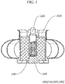
FIG. 1 , a board mating connector, which has one side in contact with a board such as a printed circuit board on which a signal wiring is formed and transmits a radio frequency (RF) signal to the board, includes asignal contact unit 100 in contact with a signal pad of the board and aground contact unit 200 in contact with a ground pad of the board. - The
signal contact unit 100 and theground contact unit 200 are separately operated. - When the board is tilted to come into contact with the board mating connector, although the
ground contact unit 200 is tilted to come into contact with the ground pad along with the ground pad of the tilted board, thesignal contact unit 100 is not tilted along with theground contact unit 200. Thus, thesignal contact unit 100 is biased to one side to come into contact with the signal pad of the board, and thus, impedance is distorted, or thesignal contact unit 100 does not come into contact with the signal pad of the board, and thus, an RF signal is not transmitted to the board. - In addition to such a problem, on the contrary, in a case in which the
signal contact unit 100 is tilted to come into contact with the signal pad along with the signal pad of the tilted board, there is a problem in that theground contact unit 200 is not tilted along with the signal pad. -
- (Patent Document 1)
KR 10-2015-0080486 A - (Patent Document 2)
KR 10-152937 B1 - (Patent Document 3)
KR 10-152937 B1 - The present invention is directed to providing a board mating connector in which a signal contact unit and a ground contact unit are interlocked.
- In one example embodiment, a board mating connector, in which a signal contact unit and a ground contact unit are interlocked, includes a signal contact unit which has one side in contact with a signal electrode of a board and is electrically connected to the signal electrode; a ground contact unit which has one side in contact with a ground electrode of the board and is electrically connected to the ground electrode; and a dielectric unit which is disposed between the signal contact unit and the ground contact unit, wherein the ground contact unit includes a ground portion and another ground portion which is relatively moved while in contact with the ground portion so as to be coupled to and interlocked with the connection portion through the dielectric unit.
- The signal contact unit may include a housing which has a housing insertion hole of which one side is open, a contact portion which has a contact portion insertion hole of which the other side is open, and a connection portion which is inserted between the one side of the housing insertion hole and the other side of the contact portion insertion hole; the ground contact unit may include a first ground portion which has a first ground hollow portion and include a second ground portion of which the other side is partially inserted into the first ground hollow portion and which has a second ground hollow portion; and the dielectric unit may include a first dielectric portion which is disposed between the housing and the first ground portion and include a second dielectric portion which is disposed between the connection portion and the second ground portion, wherein, when the second ground portion is moved in a direction of the first ground portion or in a direction opposite to the direction of the first ground portion, the connection portion is moved by the second dielectric portion in a direction in which the second ground portion is moved.
- The connection portion may include a first connection hole of which the other side is open; a second connection hole of which one side is open; a first connection protrusion which protrudes from an outer wall of the other end of the connection portion; a second connection protrusion which protrudes from an outer wall of one end of the connection portion; two or more first connection slits which are elongated to one side of the connection portion from the other end thereof along a circumference of the connection portion; and two or more second connection slits which are elongated from the one end of the connection portion to the other side thereof along the circumference of the connection portion.
- The board mating connector may further include a signal spring which is inserted between the one side of the second connection hole and the other side of the contact portion insertion hole, wherein, when the contact portion is moved in a direction of the connection portion, the signal spring is compressed by the contact portion, and the compressed signal spring is restored so that the contact portion is moved in a direction opposite to the direction of the connection portion.
- The contact portion may further include a contact tapered portion which is formed on an inner wall of the contact portion so as to have an inclined shape such that an inner diameter thereof is gradually decreased toward the other side thereof, wherein, when the contact portion is moved in a direction of the connection portion, an outer diameter of the second connection protrusion is compressed by the contact tapered portion, and the compressed outer diameter of the second connection protrusion is restored in a direction in which an inner diameter of the contact tapered portion is increased so that the contact portion is moved in a direction opposite to the direction of the connection portion.
- The second dielectric portion may include two or more second dielectric hollow portions which are formed in a hole shape passing from the other end to one end of the second dielectric portion between the connection portion and the second ground portion.
- The board mating connector may further include a ground spring which is disposed between an inner side of the first ground portion and an outer side of the second ground portion, wherein, when the second ground portion is moved in the direction of the first ground portion, the ground spring is compressed by the second ground portion, and the compressed ground spring is restored so that the second ground portion is moved in the direction opposite to the direction of the first ground portion.
- The first ground portion may include a ground tapered portion which is formed on an inner wall of the first ground portion so as to have an inclined shape such that an inner diameter thereof is gradually decreased toward the other side thereof, and the second ground portion may include a second ground protrusion which protrudes outward from the other end of the second ground portion and include two or more second ground slits which are elongated to one side of the second ground portion from the other end thereof along a circumference of the second ground portion, wherein, when the second ground portion is moved in the direction of the first ground portion, an outer diameter of the second ground protrusion is compressed by the ground tapered portion, and the compressed outer diameter of the second ground protrusion is restored in a direction in which an inner diameter of the ground tapered portion is increased so that the second ground portion is moved in the direction opposite to the direction of the first ground portion.
- The first ground portion may include a ground tapered portion which is formed on an inner wall of the first ground portion so as to have an inclined shape such that an inner diameter thereof is gradually decreased toward the other side thereof, and the second ground portion may include a second ground protrusion which protrudes outward from the other end of the second ground portion and include two or more second ground slits which are elongated to one side of the second ground portion from the other end thereof along a circumference of the second ground portion, wherein, when the second ground portion is moved in the direction of the first ground portion, an outer diameter of the second ground protrusion is compressed by the ground tapered portion, and the compressed outer diameter of the second ground protrusion is restored in a direction in which an inner diameter of the ground tapered portion is increased so that the second ground portion is moved in the direction opposite to the direction of the first ground portion.
- First, a signal contact unit and a ground contact unit come into contact with each other accurately within an allowable range in which an RF signal is transmitted to a board, and impedance is not distorted.
- In addition, one side of a contact portion stably comes into contact with a board.
- Furthermore, a change in impedance is minimized.
- In addition, a restoring force can be further increased.
- Furthermore, it is possible to lower a height of a module including a board mating connector, easily couple the board mating connector, and stably fix the board mating connector.
-
-
FIG. 1 is a cross-sectional view illustrating the related art. -
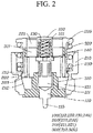
FIG. 2 is a cross-sectional view illustrating a restoration state of a board mating connector. -
FIG. 3 is a cross-sectional view illustrating a compression state of the board mating connector. -
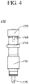
FIG. 4 is a view illustrating an exterior of a signal contact unit. -
FIG. 5 is a cross-sectional view illustrating a restoration state of the signal contact unit. -
FIG. 6 is a cross-sectional view illustrating a compression state of the signal contact unit. -
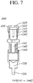
FIG. 7 is a cross-sectional view illustrating a restoration state of a signal contact unit according to another embodiment. -
FIG. 8 is a plan view illustrating a board mating connector. -
FIG. 9 is a cross-sectional view illustrating a restoration state of a board mating connector according to another embodiment. -
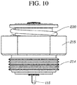
FIG. 10 is a front view illustrating a board mating connector. -
FIG. 11 is a view illustrating a state in which a board mating connector is inserted into a module. -
FIGS. 12 to 14 are views illustrating exteriors of board mating connectors. - When a
signal contact unit 100 and aground contact unit 200 are separately operated and a board is tilted and brought into contact therewith, although theground contact unit 200 is tilted to come into contact with a ground pad along with the ground pad of the tilted board, thesignal contact unit 100 is not tilted along with theground contact unit 200. Thus, thesignal contact unit 100 is biased to one side to come into contact with the signal pad of the board, whereby impedance is distorted, or thesignal contact unit 100 does not come into contact with the signal pad of the board, whereby a radio frequency (RF) signal is not transmitted to the board. - In addition to such a problem, on the contrary, in a case in which the
signal contact unit 100 is tilted to come into contact with the signal pad along with the signal pad of the tilted board, there is a problem in that theground contact unit 200 is not tilted along with the signal pad. - To solve the problems, as shown in
FIGS. 2 and3 , a board mating connector according to the present invention includes asignal contact unit 100, aground contact unit 200, and a dielectric unit 300. - One side of the
signal contact unit 100 comes into contact with a signal electrode of a board, and thus, thesignal contact unit 100 is electrically connected to the signal electrode. - One side of the
ground contact unit 200 comes into contact with a ground electrode of the board, and thus, theground contact unit 200 is electrically connected to the ground electrode. - The dielectric unit 300 is disposed between the
signal contact unit 100 and theground contact unit 200. - In this case, the
ground contact unit 200 includes afirst ground portion 210 and asecond ground portion 220, which is relatively moved in contact with thefirst ground portion 210 so as to be coupled to and interlocked with thesignal contact unit 100 through the dielectric unit 300. - As a detailed configuration which allows the
signal contact unit 100 and theground contact unit 200 to be interlocked with each other, thesignal contact unit 100 includes ahousing 110, acontact portion 120, and aconnection portion 140. - In addition, the
ground contact unit 200 includes thefirst ground portion 210 and thesecond ground portion 220. - Furthermore, the dielectric unit 300 includes a first
dielectric portion 310 and a seconddielectric portion 320. - First, describing the components of the
signal contact unit 100, thehousing 110 has ahousing insertion hole 111 of which one side is open and includes acontact pin 115 formed at the other end thereof. - The
contact portion 120 has a contactportion insertion hole 121 of which the other side is open. - The
connection portion 140 is inserted between one side of thehousing insertion hole 111 and the other side of the contactportion insertion hole 121. - Next, describing the components of the
ground contact unit 200, a first groundhollow portion 211 is formed in thefirst ground portion 210. For example, the other end of theconnection portion 140 is inserted to be movable along an inner side of thehousing insertion hole 111, and one end of theconnection portion 140 is inserted to be movable along an inner side of the contactportion insertion hole 121. - The other side of the
second ground portion 220 is partially inserted into the first groundhollow portion 211, and a second groundhollow portion 221 is formed in thesecond ground portion 220. - Describing the components of the dielectric unit 300, the first
dielectric portion 310 is disposed between thehousing 110 and thefirst ground portion 210. - The second
dielectric portion 320 is disposed between theconnection portion 140 and thesecond ground portion 220. - Due to such a configuration, as shown in
FIG. 3 , when thesecond ground portion 220 is moved in the direction of thefirst ground portion 210 or a direction opposite to the direction of thefirst ground portion 210, the seconddielectric portion 320 allows theconnection portion 140 to be moves together with thesecond ground portion 220 in a direction in which thesecond ground portion 220 is moved. - As described above, since the
signal contact unit 100 and theground contact unit 200 are interlocked with each other, thesignal contact unit 100 and theground contact unit 200 are connected accurately within an allowable range in which an RF signal is transmitted to a board, and impedance is not distorted. - As shown in
FIGS. 4 to 6 , theconnection portion 140 includes afirst connection hole 141, asecond connection hole 142, afirst connection protrusion 143, asecond connection protrusion 144, a first connection slit 145, and a second connection slit 146. - The
first connection hole 141 is formed in theconnection portion 140 so as to have the other side which is open. - The
second connection hole 142 is formed in theconnection portion 140 so as to have one side which is open. - The
first connection protrusion 143 is formed to protrude from an outer wall of the other end of theconnection portion 140. - The
second connection protrusion 144 is formed to protrude from an outer wall of one end of theconnection portion 140. - The first connection slit 145 is elongated to one side of the
connection portion 140 from the other end thereof. Two or more first connection slits 145 are formed along a circumference of theconnection portion 140 such that the other end of theconnection portion 140 is divided into a plurality of portions. - The second connection slit 146 is elongated from one end of the
connection portion 140 to the other side thereof. Two or more second connection slits 146 are formed along the circumference of theconnection portion 140 such that one end of theconnection portion 140 is divided into a plurality of portions. - Due to such a configuration, as shown in
FIG. 6 , in a state in which one side of thecontact portion 120 comes into contact with the board and thesignal contact unit 100 is compressed, thefirst connection protrusion 143 comes into contact with an inner side of thehousing 110, and thesecond connection protrusion 144 comes into contact with an inner side of thecontact portion 120. Accordingly, thehousing 110 and thecontact portion 120 are electrically connected through theconnection portion 140. - A component may be further provided to provide elasticity such that one side of the
contact portion 120 stably comes into contact with the board. - As such an elastic structure, a
signal spring 130 may be further provided as shown inFIGS. 5 and6 , or a contact taperedportion 122 may be further included in thecontact portion 120 as shown inFIG. 7 . - The
signal spring 130 is inserted between one side of thesecond connection hole 142 and the other side of the contactportion insertion hole 121. - In this case, when the
contact portion 120 is moved in the direction of theconnection portion 140, thesignal spring 130 is compressed by thecontact portion 120, and thecompressed signal spring 130 is restored. Thus, thecontact portion 120 is moved in a direction opposite to the direction of theconnection portion 140. - The contact tapered
portion 122 is formed in an inclined shape such that an inner diameter thereof is gradually decreased toward one side thereof on an inner wall of thecontact portion 120. - In this case, when the
contact portion 120 is moved in the direction of theconnection portion 140, an outer diameter of thesecond connection protrusion 144 is compressed by the contact taperedportion 122, and the compressed outer diameter of thesecond connection protrusion 144 is restored in a direction in which an inner diameter of the contact taperedportion 122 is increased. Thus, thecontact portion 120 is moved in the direction opposite to the direction of theconnection portion 140. - As described above, the component is further provided to provide elasticity when one side of the
contact portion 120 comes into contact with the board, whereby one side of thecontact portion 120 stably comes into contact with the board. - As shown in
FIGS. 2 ,3 , and8 , the seconddielectric portion 320 includes a second dielectrichollow portion 321. - The second dielectric
hollow portion 321 is formed in a hole shape passing from the other end to one end of the seconddielectric portion 320. Two or more second dielectrichollow portions 321 are formed between theconnection portion 140 and thesecond ground portion 220. - As shown in
FIG. 3 , when thesecond ground portion 220 is moved in the direction of thefirst ground portion 210 and when the seconddielectric portion 320 approaches the firstdielectric portion 310, in order to minimize a change in impedance, which is caused by a dielectric constant of the seconddielectric portion 320 being added to a dielectric constant of the firstdielectric portion 310, the second dielectrichollow portion 321 is formed in the seconddielectric portion 320. Accordingly, an area of the seconddielectric portion 320 is decreased. - Therefore, it is possible to minimize the change in impedance.
- As shown in
FIGS. 2 and3 , the board mating connector according to the present invention further includes aground spring 230 disposed between an inner side of thefirst ground portion 210 and an outer side of thesecond ground portion 220. - As shown in
FIG. 3 , when one side of theground contact unit 200 comes into contact with the board and thesecond ground portion 220 is moved in the direction of thefirst ground portion 210, theground spring 230 is compressed by thesecond ground portion 220, and thecompressed ground spring 230 is restored. Thus, thesecond ground portion 220 is moved in the direction opposite to the direction of thefirst ground portion 210. - As shown in
FIGS. 2 and3 , a restoring force to move thesecond ground portion 220 in the direction opposite to the direction of thefirst ground portion 210 may be further increased. Alternatively, as shown inFIG. 9 , in order to replace theground spring 230 described above, thefirst ground portion 210 may include a ground taperedportion 212, and thesecond ground portion 220 may include asecond ground protrusion 222 and a second ground slit 223. - The ground tapered
portion 212 is formed in an inclined shape such that an inner diameter thereof is gradually decreased toward the other side thereof on an inner wall of thefirst ground portion 210. - The
second ground protrusion 222 protrudes outward from the other end of the second ground portion. - The second ground slit 223 is elongated to one side of the second ground portion from the other end thereof. Two or more second ground slits 223 are formed along a circumference of the second ground portion such that the other end of the
second ground portion 220 is divided into a plurality of portions. - When the
second ground portion 220 is moved in the direction of thefirst ground portion 210, an outer diameter of thesecond ground protrusion 222 is compressed by the ground taperedportion 212, and the compressed outer diameter of thesecond ground protrusion 222 is restored in a direction in which an inner diameter of the ground taperedportion 212 is increased, and thus, thesecond ground portion 220 is moved in the direction opposite to the direction of thefirst ground portion 210. - In this case, in order to prevent the
second ground portion 220 from being moved more than necessary in the direction opposite to the direction of thefirst ground portion 210, alatch portion 213 may be formed to protrude inward from a wall of thefirst ground portion 210 at one side of the wall of thefirst ground portion 210 with respect to a position where the tapered portion 224 is formed. - One side of the
second ground protrusion 222 may be caught by thelatch portion 213, and thus, thelatch portion 213 may prevent thesecond ground portion 220 from being further moved in the direction opposite to the direction of thefirst ground portion 210. - As described above, as shown in
FIGS. 2 and3 , when the above-describedground spring 230 is further provided, a restoring force due to theground spring 230 may be added to a restoring force in which thesecond ground portion 220 is moved in the direction opposite to the direction of thefirst ground portion 210 by the ground taperedportion 212, thesecond ground protrusion 222, and the second ground slit 223. - Accordingly, it is possible to further increase the restoring force to move the
second ground portion 220 in the direction opposite to the direction of thefirst ground portion 210. - In addition, as shown in
FIG. 9 , when the above-describedground spring 230 is not provided, the ground taperedportion 212, thesecond ground protrusion 222, and the second ground slit 223 may replace theground spring 230. - As shown in
FIGS. 8 ,10 , and11 , thefirst ground portion 210 may include athread 214 and a tighteningportion 215 such that one side of the board mating connector according to the present invention is insertion-coupled to a module using a tool such as a wrench. - The
thread 214 is formed on a circumference of the other side of thefirst ground portion 210. - The tightening
portion 215 is formed to have three or more surfaces on a circumference of one side of thefirst ground portion 210. - As shown in
FIG. 11 , a module M has a hole H which has a wall corresponding to thethread 214, and the board mating connector is inserted into the hole H. - Here, the
contact pin 115 may be electrically connected to a signal electrode pin P protruding toward a center of the hole H. - A board B comes into contact with one side of the board mating connector, and thus, the board mating connector transmits an RF signal to the board B.
- As described above, since the
thread 214 and the tighteningportion 215 are provided such that one side of the board mating connector is insertion-coupled to the module, a contact height of the board B may be lowered. Thus, it is possible to lower a height of the module M including the board mating connector, easily couple the board mating connector, and stably fix the board mating connector. - An exterior of the board mating connector according to the present invention is not limited to the above-described shape including the
thread 214 and the tighteningportion 215 and may be formed in various shapes as shown inFIGS. 12 and14 . - As shown in
FIG. 12 , a shape of thefirst ground portion 210 is formed in a cylindrical shape in which a plurality of press-fit protrusions PB are formed at one side of thefirst ground portion 210 such that thefirst ground portion 210 is press-fitted into the module. - As shown in
FIG. 13 , thefirst ground portion 210 is formed in a panel shape in which grooves, to which screws are coupled, are formed on both sides thereof such that thefirst ground portion 210 is screw-coupled to the module. - As shown in
FIG. 14 , thefirst ground portion 210 is formed in a shape in which a plurality of ground pins GP inserted into a printed circuit board (PCB) soldering hole are formed such that thefirst ground portion 210 is soldered to a PCB. -
- 100: signal contact unit 110: housing
- 111: housing insertion hole 115: contact pin
- 120: contact portion 121: contact portion insertion hole
- 122: contact tapered portion 130: signal spring
- 140: connection portion 141: first connection hole
- 142: second connection hole 143: first connection protrusion
- 144: second connection protrusion 145: first connection slit
- 146: second connection slit 200: ground contact unit
- 210: first ground portion 211: first ground hollow portion
- 212: ground tapered portion 213: latch portion
- 214: thread 215: tightening portion
- 220: second ground portion 221: second ground hollow portion
- 222: second ground protrusion 223: second ground slit
- 230: ground spring 300: dielectric unit
- 310: first dielectric portion 320: second dielectric portion
- 321: second dielectric hollow portion
Claims (9)
- A board mating connector in which a signal contact unit (100) and a ground contact unit (200) are interlocked, the board mating connector comprising:a signal contact unit (100) which has one side in contact with a signal electrode of a board and is electrically connected to the signal electrode;a ground contact unit (200) which has one side in contact with a ground electrode of the board and is electrically connected to the ground electrode; anda dielectric unit (300) which is disposed between the signal contact unit (100) and the ground contact unit (200),wherein the signal contact unit (100) includes a housing (110) which has a housing insertion hole (111) of which one side is open, a contact portion (120) which has a contact portion insertion hole (121) of which the other side is open, and a connection portion (140) which has the other end inserted to be movable along an inner side of the housing insertion hole (111) and one end inserted to be movable along an inner side of the contact portion insertion hole (121), andthe ground contact unit (200) includes a first ground portion (210) and a second ground portion (220) which is relatively moved while in contact with the first ground portion (210) so as to be coupled to and interlocked with the connection portion (140) through the dielectric unit (300).
- The board mating connector of claim 1, wherein:the first ground portion (210) which has a first ground hollow portion (211),the other side of the second ground portion (220) which is partially inserted into the first ground hollow portion (211) and which has a second ground hollow portion (221),the dielectric unit (300) includes a first dielectric portion (310) which is disposed between the housing (110) and the first ground portion (210) and a second dielectric portion (320) which is disposed between the connection portion (140) and the second ground portion (220),wherein, when the second ground portion (220) is moved in a direction of the first ground portion (210) or in a direction opposite to the direction of the first ground portion (210), the connection portion (140) is moves together with the second ground portion (220) by the second dielectric portion (320) in a direction in which the second ground portion (220) is moved.
- The board mating connector of claim 2, wherein:the connection portion (140) includes a first connection hole (141) of which the other side is open;a second connection hole (142) of which one side is open;a first connection protrusion (143) which protrudes from an outer wall of the other end of the connection portion (140);a second connection protrusion (144) which protrudes from an outer wall of one end of the connection portion (140);two or more first connection slits (145) which are elongated to one side of the connection portion (140) from the other end thereof along a circumference of the connection portion (140); andtwo or more second connection slits (146) which are elongated from the one end of the connection portion (140) to the other side thereof along the circumference of the connection portion (140).
- The board mating connector of claim 3, further comprising a signal spring (130) which is inserted between the one side of the second connection hole (142) and the other side of the contact portion insertion hole (121),
wherein, when the contact portion (120) is moved in a direction of the connection portion (140), the signal spring (130) is compressed by the contact portion (120), and the compressed signal spring (130) is restored so that the contact portion (120) is moved in a direction opposite to the direction of the connection portion (140). - The board mating connector of claim 3, wherein the contact portion (120) further includes a contact tapered portion (122) which is formed on an inner wall of the contact portion (120) so as to have an inclined shape such that an inner diameter thereof is gradually decreased toward the other side thereof,
wherein, when the contact portion (120) is moved in a direction of the connection portion (140), an outer diameter of the second connection protrusion (144) is compressed by the contact tapered portion (122), and the compressed outer diameter of the second connection protrusion (144) is restored in a direction in which an inner diameter of the contact tapered portion (122) is increased so that the contact portion (120) is moved in a direction opposite to the direction of the connection portion (140). - The board mating connector of claim 3, wherein the second dielectric portion (320) includes two or more second dielectric hollow portions (321) which are formed in a hole shape passing from the other end to one end of the second dielectric portion (320) between the connection portion (140) and the second ground portion (220).
- The board mating connector of any one of claims 2 to 6, further comprising a ground spring (230) which is disposed between an inner side of the first ground portion (210) and an outer side of the second ground portion (220),
wherein, when the second ground portion (220) is moved in the direction of the first ground portion (210), the ground spring (230) is compressed by the second ground portion (220), and the compressed ground spring (230) is restored so that the second ground portion (220) is moved in the direction opposite to the direction of the first ground portion (210). - The board mating connector of claim 7, wherein:the first ground portion (210) includes a ground tapered portion (212) which is formed on an inner wall of the first ground portion (210) so as to have an inclined shape such that an inner diameter thereof is gradually decreased toward the other side thereof; andthe second ground portion (220) includes a second ground protrusion (222) which protrudes outward from the other end of the second ground portion (220), and two or more second ground slits (223) which are elongated to one side of the second ground portion (220) from the other end thereof along a circumference of the second ground portion (220),wherein, when the second ground portion (220) is moved in the direction of the first ground portion (210), an outer diameter of the second ground protrusion (222) is compressed by the ground tapered portion (212), and the compressed outer diameter of the second ground protrusion (222) is restored in a direction in which an inner diameter of the ground tapered portion (212) is increased so that the second ground portion (220) is moved in the direction opposite to the direction of the first ground portion (210).
- The board mating connector of any one of claims 2 to 6, wherein:the first ground portion (210) includes a ground tapered portion (212) which is formed on an inner wall of the first ground portion (210) so as to have an inclined shape such that an inner diameter thereof is gradually decreased toward the other side thereof; andthe second ground portion (220) includes a second ground protrusion (222) which protrudes outward from the other end of the second ground portion (220), and two or more second ground slits (223) which are elongated to one side of the second ground portion (220) from the other end thereof along a circumference of the second ground portion (220),wherein, when the second ground portion (220) is moved in the direction of the first ground portion (210), an outer diameter of the second ground protrusion (222) is compressed by the ground tapered portion (212), and the compressed outer diameter of the second ground protrusion (222) is restored in a direction in which an inner diameter of the ground tapered portion (212) is increased so that the second ground portion (220) is moved in the direction opposite to the direction of the first ground portion (210).
Applications Claiming Priority (1)
| Application Number | Priority Date | Filing Date | Title |
|---|---|---|---|
| KR1020180034834A KR101926503B1 (en) | 2018-03-27 | 2018-03-27 | Board mating connector in which the signal contact part and ground contact part are interlock |
Publications (2)
| Publication Number | Publication Date |
|---|---|
| EP3547459A1 true EP3547459A1 (en) | 2019-10-02 |
| EP3547459B1 EP3547459B1 (en) | 2020-09-16 |
Family
ID=64669668
Family Applications (1)
| Application Number | Title | Priority Date | Filing Date |
|---|---|---|---|
| EP19163690.1A Active EP3547459B1 (en) | 2018-03-27 | 2019-03-19 | Board mating connector in which signal contact unit and ground contact unit are interlocked |
Country Status (5)
| Country | Link |
|---|---|
| US (1) | US10804635B2 (en) |
| EP (1) | EP3547459B1 (en) |
| JP (1) | JP6550686B1 (en) |
| KR (1) | KR101926503B1 (en) |
| CN (1) | CN110311239B (en) |
Cited By (1)
| Publication number | Priority date | Publication date | Assignee | Title |
|---|---|---|---|---|
| EP3819993A1 (en) * | 2019-11-08 | 2021-05-12 | Gigalane Co. Ltd | Connector having joint with limited range of motion |
Families Citing this family (23)
| Publication number | Priority date | Publication date | Assignee | Title |
|---|---|---|---|---|
| CN107431301B (en) | 2015-02-06 | 2021-03-30 | 迈心诺公司 | Connector assembly with retractable needle for use with medical sensors |
| MX382951B (en) | 2015-02-06 | 2025-03-13 | Masimo Corp | Flexible foldable circuit for low noise optical probe (LNOP) |
| KR101992258B1 (en) * | 2017-10-13 | 2019-06-25 | 주식회사 케이엠더블유 | Coaxial connector |
| USD908097S1 (en) * | 2018-03-27 | 2021-01-19 | Gigalane Co., Ltd. | Signal transmission connector |
| CN111463598A (en) * | 2019-01-22 | 2020-07-28 | 罗森伯格亚太电子有限公司 | Radio frequency coaxial elastic connector |
| CN111509446A (en) * | 2019-01-31 | 2020-08-07 | 泰科电子(上海)有限公司 | Connector |
| CN109841999B (en) * | 2019-02-22 | 2024-06-07 | 中航富士达科技股份有限公司 | Self-adaptive inter-board radio frequency connector |
| KR102037689B1 (en) * | 2019-03-28 | 2019-10-29 | 주식회사 텔콘알에프제약 | A flat contact type RF terminal |
| KR102118829B1 (en) * | 2019-07-26 | 2020-06-04 | 주식회사 기가레인 | Board-mating connector |
| CN112421278A (en) * | 2019-08-23 | 2021-02-26 | 泰科电子(上海)有限公司 | Electrical connector and electrical connector assembly |
| CN112787121A (en) * | 2019-11-11 | 2021-05-11 | 康普技术有限责任公司 | Coaxial connector and board-to-board connector assembly |
| KR102897976B1 (en) * | 2019-12-27 | 2025-12-16 | 주식회사 기가레인 | Board mating connector |
| KR102163379B1 (en) * | 2019-12-27 | 2020-10-08 | 주식회사 기가레인 | Board mating connector |
| CN111146617B (en) * | 2020-01-17 | 2025-06-27 | 东莞市维康汽车电子有限公司 | Multi-directional high tolerance coaxial connector |
| US11515669B2 (en) * | 2020-03-11 | 2022-11-29 | Te Connectivity Solutions Gmbh | Floating header and circuit board assembly |
| KR102421924B1 (en) | 2020-04-29 | 2022-07-21 | 주식회사 케이엠더블유 | Connecting apparatus |
| US11539167B2 (en) * | 2020-09-17 | 2022-12-27 | Carlisle Interconnect Technologies, Inc. | Adjustable push on connector/adaptor |
| KR102375210B1 (en) | 2020-12-21 | 2022-03-16 | 주식회사 기가레인 | Connector and board connecting assembly comprising the same |
| CN115735303A (en) * | 2020-12-21 | 2023-03-03 | 吉佳蓝科技股份有限公司 | Board connection connector and board connection assembly with same |
| EP4298699A4 (en) * | 2021-02-24 | 2025-01-08 | Smiths Interconnect Americas, Inc. | Systems and methods for coaxial board to board connections |
| DE102021002030A1 (en) * | 2021-04-17 | 2022-10-20 | Kostal Kontakt Systeme Gmbh | connection unit |
| KR102584061B1 (en) * | 2021-08-18 | 2023-10-06 | 주식회사 비마 | Plug connector for preventing misalignment with jack connector |
| CN115864029B (en) * | 2021-09-24 | 2024-03-05 | 吉佳蓝科技股份有限公司 | Fixed connectors and connector assemblies having the same |
Citations (5)
| Publication number | Priority date | Publication date | Assignee | Title |
|---|---|---|---|---|
| KR0152937B1 (en) | 1995-08-14 | 1998-12-01 | 문정환 | Method of fabricating semiconductor device |
| EP1289076A2 (en) * | 2001-08-31 | 2003-03-05 | Tyco Electronics AMP GmbH | Coaxial connector for interconnecting printed circuit boards |
| US20080057782A1 (en) * | 2006-08-31 | 2008-03-06 | Radiall | Coaxial connector for interconnecting two printed circuit cards |
| CN104466484A (en) * | 2014-12-26 | 2015-03-25 | 廖芳 | Novel pogo pin |
| KR20150080486A (en) | 2012-10-29 | 2015-07-09 | 로젠버거 호흐프리쿠벤츠테흐닉 게엠베하 운트 코. 카게 | Contact element for transmitting high-frequency signals between two circuit boards |
Family Cites Families (15)
| Publication number | Priority date | Publication date | Assignee | Title |
|---|---|---|---|---|
| US4815986A (en) * | 1987-08-14 | 1989-03-28 | Lucas Weinschel, Inc. | Self-aligning blind mate connector |
| JP2586334B2 (en) | 1994-06-08 | 1997-02-26 | 日本電気株式会社 | Contact type high frequency signal connection structure |
| JP3126892B2 (en) | 1995-02-27 | 2001-01-22 | 株式会社ヨコオ | Coaxial board connector |
| DE29517358U1 (en) * | 1995-11-02 | 1996-01-11 | Harting Elektronik Gmbh, 32339 Espelkamp | Coaxial connector |
| US5769652A (en) * | 1996-12-31 | 1998-06-23 | Applied Engineering Products, Inc. | Float mount coaxial connector |
| FR2758662B1 (en) * | 1997-01-20 | 1999-03-26 | Radiall Sa | MOBILE CONTACT COAXIAL ELECTRIC CONNECTOR ELEMENT AND COAXIAL ELECTRIC CONNECTOR INCLUDING SUCH A CONNECTOR ELEMENT |
| DE50002830D1 (en) * | 1999-03-02 | 2003-08-14 | Huber & Suhner Ag Herisau | LEITERPLATTEN-coaxial |
| JP4428803B2 (en) | 2000-04-17 | 2010-03-10 | 株式会社ヨコオ | Electrical connection device and connection unit |
| KR101116488B1 (en) * | 2004-05-17 | 2012-03-07 | 가부시끼가이샤 와꼬 세이끼 | Conductive pin |
| JP2006092999A (en) * | 2004-09-27 | 2006-04-06 | Staf Corp | Coaxial connector and cap used for it |
| JP3107906U (en) | 2004-09-27 | 2005-04-07 | スタッフ株式会社 | Coaxial connector |
| TWI291269B (en) * | 2006-01-13 | 2007-12-11 | Murata Manufacturing Co | Coaxial connector and coaxial probe for measurement |
| KR101326296B1 (en) * | 2012-02-27 | 2013-11-11 | 주식회사 텔콘 | Rf connector for substrates |
| US8747152B2 (en) * | 2012-11-09 | 2014-06-10 | Andrew Llc | RF isolated capacitively coupled connector |
| US20180040993A1 (en) | 2016-01-13 | 2018-02-08 | Shanghai Radiall Electronics Co., Ltd. | Coaxial connection system for rf signals with high rf performance levels |
-
2018
- 2018-03-27 KR KR1020180034834A patent/KR101926503B1/en active Active
-
2019
- 2019-03-12 CN CN201910183181.9A patent/CN110311239B/en active Active
- 2019-03-19 EP EP19163690.1A patent/EP3547459B1/en active Active
- 2019-03-22 US US16/361,434 patent/US10804635B2/en active Active
- 2019-03-26 JP JP2019058275A patent/JP6550686B1/en active Active
Patent Citations (5)
| Publication number | Priority date | Publication date | Assignee | Title |
|---|---|---|---|---|
| KR0152937B1 (en) | 1995-08-14 | 1998-12-01 | 문정환 | Method of fabricating semiconductor device |
| EP1289076A2 (en) * | 2001-08-31 | 2003-03-05 | Tyco Electronics AMP GmbH | Coaxial connector for interconnecting printed circuit boards |
| US20080057782A1 (en) * | 2006-08-31 | 2008-03-06 | Radiall | Coaxial connector for interconnecting two printed circuit cards |
| KR20150080486A (en) | 2012-10-29 | 2015-07-09 | 로젠버거 호흐프리쿠벤츠테흐닉 게엠베하 운트 코. 카게 | Contact element for transmitting high-frequency signals between two circuit boards |
| CN104466484A (en) * | 2014-12-26 | 2015-03-25 | 廖芳 | Novel pogo pin |
Cited By (2)
| Publication number | Priority date | Publication date | Assignee | Title |
|---|---|---|---|---|
| EP3819993A1 (en) * | 2019-11-08 | 2021-05-12 | Gigalane Co. Ltd | Connector having joint with limited range of motion |
| US11411360B2 (en) | 2019-11-08 | 2022-08-09 | Gigalane Co., Ltd. | Connector having joint with limited range of motion |
Also Published As
| Publication number | Publication date |
|---|---|
| US20190305457A1 (en) | 2019-10-03 |
| JP6550686B1 (en) | 2019-07-31 |
| KR101926503B1 (en) | 2018-12-07 |
| US10804635B2 (en) | 2020-10-13 |
| CN110311239A (en) | 2019-10-08 |
| JP2019175849A (en) | 2019-10-10 |
| EP3547459B1 (en) | 2020-09-16 |
| CN110311239B (en) | 2020-11-10 |
Similar Documents
| Publication | Publication Date | Title |
|---|---|---|
| US10804635B2 (en) | Board mating connector in which signal contact unit and ground contact unit are interlocked | |
| EP3547460A1 (en) | Board mating connector | |
| KR100756802B1 (en) | Coaxial connector for connection between substrates | |
| EP4059098A1 (en) | Coaxial connector and board-to-board connector assembly | |
| CN1938905A (en) | Coaxial plug-in connection for printed boards, featuring spring-loaded tolerance compensation | |
| KR20040024591A (en) | Self-adjusted subminiature coaxial connector | |
| CN109980384B (en) | Substrate mating connector including ground portion formed with tapered portion | |
| US6805575B2 (en) | Guide system for contact plugs | |
| US20040087202A1 (en) | Slotted guide pin and latch assembly | |
| KR20180054230A (en) | Coaxial connector plug and RF connector including the same | |
| US9502825B2 (en) | Shunt for electrical connector | |
| US12095184B2 (en) | Connector and connector assembly | |
| JP2021114397A (en) | connector | |
| KR20200039558A (en) | Contact module and plug connector having the same | |
| US20250323462A1 (en) | Electrical connector | |
| KR20180077505A (en) | Board to Board Connector | |
| KR101532399B1 (en) | Conector for printed circuit board |
Legal Events
| Date | Code | Title | Description |
|---|---|---|---|
| PUAI | Public reference made under article 153(3) epc to a published international application that has entered the european phase |
Free format text: ORIGINAL CODE: 0009012 |
|
| STAA | Information on the status of an ep patent application or granted ep patent |
Free format text: STATUS: REQUEST FOR EXAMINATION WAS MADE |
|
| 17P | Request for examination filed |
Effective date: 20190319 |
|
| AK | Designated contracting states |
Kind code of ref document: A1 Designated state(s): AL AT BE BG CH CY CZ DE DK EE ES FI FR GB GR HR HU IE IS IT LI LT LU LV MC MK MT NL NO PL PT RO RS SE SI SK SM TR |
|
| AX | Request for extension of the european patent |
Extension state: BA ME |
|
| RBV | Designated contracting states (corrected) |
Designated state(s): AL AT BE BG CH CY CZ DE DK EE ES FI FR GB GR HR HU IE IS IT LI LT LU LV MC MK MT NL NO PL PT RO RS SE SI SK SM TR |
|
| RIC1 | Information provided on ipc code assigned before grant |
Ipc: H01R 12/91 20110101AFI20200409BHEP Ipc: H01R 13/24 20060101ALI20200409BHEP Ipc: H01R 103/00 20060101ALN20200409BHEP Ipc: H01R 24/50 20110101ALI20200409BHEP |
|
| GRAP | Despatch of communication of intention to grant a patent |
Free format text: ORIGINAL CODE: EPIDOSNIGR1 |
|
| STAA | Information on the status of an ep patent application or granted ep patent |
Free format text: STATUS: GRANT OF PATENT IS INTENDED |
|
| INTG | Intention to grant announced |
Effective date: 20200515 |
|
| GRAS | Grant fee paid |
Free format text: ORIGINAL CODE: EPIDOSNIGR3 |
|
| GRAA | (expected) grant |
Free format text: ORIGINAL CODE: 0009210 |
|
| STAA | Information on the status of an ep patent application or granted ep patent |
Free format text: STATUS: THE PATENT HAS BEEN GRANTED |
|
| AK | Designated contracting states |
Kind code of ref document: B1 Designated state(s): AL AT BE BG CH CY CZ DE DK EE ES FI FR GB GR HR HU IE IS IT LI LT LU LV MC MK MT NL NO PL PT RO RS SE SI SK SM TR |
|
| REG | Reference to a national code |
Ref country code: GB Ref legal event code: FG4D |
|
| REG | Reference to a national code |
Ref country code: CH Ref legal event code: EP |
|
| REG | Reference to a national code |
Ref country code: DE Ref legal event code: R096 Ref document number: 602019000678 Country of ref document: DE |
|
| REG | Reference to a national code |
Ref country code: IE Ref legal event code: FG4D |
|
| REG | Reference to a national code |
Ref country code: AT Ref legal event code: REF Ref document number: 1314990 Country of ref document: AT Kind code of ref document: T Effective date: 20201015 |
|
| PG25 | Lapsed in a contracting state [announced via postgrant information from national office to epo] |
Ref country code: SE Free format text: LAPSE BECAUSE OF FAILURE TO SUBMIT A TRANSLATION OF THE DESCRIPTION OR TO PAY THE FEE WITHIN THE PRESCRIBED TIME-LIMIT Effective date: 20200916 Ref country code: FI Free format text: LAPSE BECAUSE OF FAILURE TO SUBMIT A TRANSLATION OF THE DESCRIPTION OR TO PAY THE FEE WITHIN THE PRESCRIBED TIME-LIMIT Effective date: 20200916 Ref country code: GR Free format text: LAPSE BECAUSE OF FAILURE TO SUBMIT A TRANSLATION OF THE DESCRIPTION OR TO PAY THE FEE WITHIN THE PRESCRIBED TIME-LIMIT Effective date: 20201217 Ref country code: NO Free format text: LAPSE BECAUSE OF FAILURE TO SUBMIT A TRANSLATION OF THE DESCRIPTION OR TO PAY THE FEE WITHIN THE PRESCRIBED TIME-LIMIT Effective date: 20201216 Ref country code: BG Free format text: LAPSE BECAUSE OF FAILURE TO SUBMIT A TRANSLATION OF THE DESCRIPTION OR TO PAY THE FEE WITHIN THE PRESCRIBED TIME-LIMIT Effective date: 20201216 Ref country code: HR Free format text: LAPSE BECAUSE OF FAILURE TO SUBMIT A TRANSLATION OF THE DESCRIPTION OR TO PAY THE FEE WITHIN THE PRESCRIBED TIME-LIMIT Effective date: 20200916 |
|
| REG | Reference to a national code |
Ref country code: AT Ref legal event code: MK05 Ref document number: 1314990 Country of ref document: AT Kind code of ref document: T Effective date: 20200916 |
|
| REG | Reference to a national code |
Ref country code: NL Ref legal event code: MP Effective date: 20200916 |
|
| PG25 | Lapsed in a contracting state [announced via postgrant information from national office to epo] |
Ref country code: RS Free format text: LAPSE BECAUSE OF FAILURE TO SUBMIT A TRANSLATION OF THE DESCRIPTION OR TO PAY THE FEE WITHIN THE PRESCRIBED TIME-LIMIT Effective date: 20200916 Ref country code: LV Free format text: LAPSE BECAUSE OF FAILURE TO SUBMIT A TRANSLATION OF THE DESCRIPTION OR TO PAY THE FEE WITHIN THE PRESCRIBED TIME-LIMIT Effective date: 20200916 |
|
| REG | Reference to a national code |
Ref country code: LT Ref legal event code: MG4D |
|
| PG25 | Lapsed in a contracting state [announced via postgrant information from national office to epo] |
Ref country code: LT Free format text: LAPSE BECAUSE OF FAILURE TO SUBMIT A TRANSLATION OF THE DESCRIPTION OR TO PAY THE FEE WITHIN THE PRESCRIBED TIME-LIMIT Effective date: 20200916 Ref country code: SM Free format text: LAPSE BECAUSE OF FAILURE TO SUBMIT A TRANSLATION OF THE DESCRIPTION OR TO PAY THE FEE WITHIN THE PRESCRIBED TIME-LIMIT Effective date: 20200916 Ref country code: EE Free format text: LAPSE BECAUSE OF FAILURE TO SUBMIT A TRANSLATION OF THE DESCRIPTION OR TO PAY THE FEE WITHIN THE PRESCRIBED TIME-LIMIT Effective date: 20200916 Ref country code: RO Free format text: LAPSE BECAUSE OF FAILURE TO SUBMIT A TRANSLATION OF THE DESCRIPTION OR TO PAY THE FEE WITHIN THE PRESCRIBED TIME-LIMIT Effective date: 20200916 Ref country code: PT Free format text: LAPSE BECAUSE OF FAILURE TO SUBMIT A TRANSLATION OF THE DESCRIPTION OR TO PAY THE FEE WITHIN THE PRESCRIBED TIME-LIMIT Effective date: 20210118 Ref country code: CZ Free format text: LAPSE BECAUSE OF FAILURE TO SUBMIT A TRANSLATION OF THE DESCRIPTION OR TO PAY THE FEE WITHIN THE PRESCRIBED TIME-LIMIT Effective date: 20200916 |
|
| PG25 | Lapsed in a contracting state [announced via postgrant information from national office to epo] |
Ref country code: AT Free format text: LAPSE BECAUSE OF FAILURE TO SUBMIT A TRANSLATION OF THE DESCRIPTION OR TO PAY THE FEE WITHIN THE PRESCRIBED TIME-LIMIT Effective date: 20200916 Ref country code: AL Free format text: LAPSE BECAUSE OF FAILURE TO SUBMIT A TRANSLATION OF THE DESCRIPTION OR TO PAY THE FEE WITHIN THE PRESCRIBED TIME-LIMIT Effective date: 20200916 Ref country code: ES Free format text: LAPSE BECAUSE OF FAILURE TO SUBMIT A TRANSLATION OF THE DESCRIPTION OR TO PAY THE FEE WITHIN THE PRESCRIBED TIME-LIMIT Effective date: 20200916 Ref country code: IS Free format text: LAPSE BECAUSE OF FAILURE TO SUBMIT A TRANSLATION OF THE DESCRIPTION OR TO PAY THE FEE WITHIN THE PRESCRIBED TIME-LIMIT Effective date: 20210116 |
|
| REG | Reference to a national code |
Ref country code: DE Ref legal event code: R097 Ref document number: 602019000678 Country of ref document: DE |
|
| PG25 | Lapsed in a contracting state [announced via postgrant information from national office to epo] |
Ref country code: SK Free format text: LAPSE BECAUSE OF FAILURE TO SUBMIT A TRANSLATION OF THE DESCRIPTION OR TO PAY THE FEE WITHIN THE PRESCRIBED TIME-LIMIT Effective date: 20200916 |
|
| PLBE | No opposition filed within time limit |
Free format text: ORIGINAL CODE: 0009261 |
|
| STAA | Information on the status of an ep patent application or granted ep patent |
Free format text: STATUS: NO OPPOSITION FILED WITHIN TIME LIMIT |
|
| 26N | No opposition filed |
Effective date: 20210617 |
|
| PG25 | Lapsed in a contracting state [announced via postgrant information from national office to epo] |
Ref country code: DK Free format text: LAPSE BECAUSE OF FAILURE TO SUBMIT A TRANSLATION OF THE DESCRIPTION OR TO PAY THE FEE WITHIN THE PRESCRIBED TIME-LIMIT Effective date: 20200916 Ref country code: SI Free format text: LAPSE BECAUSE OF FAILURE TO SUBMIT A TRANSLATION OF THE DESCRIPTION OR TO PAY THE FEE WITHIN THE PRESCRIBED TIME-LIMIT Effective date: 20200916 |
|
| REG | Reference to a national code |
Ref country code: DE Ref legal event code: R119 Ref document number: 602019000678 Country of ref document: DE |
|
| PG25 | Lapsed in a contracting state [announced via postgrant information from national office to epo] |
Ref country code: MC Free format text: LAPSE BECAUSE OF FAILURE TO SUBMIT A TRANSLATION OF THE DESCRIPTION OR TO PAY THE FEE WITHIN THE PRESCRIBED TIME-LIMIT Effective date: 20200916 Ref country code: IT Free format text: LAPSE BECAUSE OF FAILURE TO SUBMIT A TRANSLATION OF THE DESCRIPTION OR TO PAY THE FEE WITHIN THE PRESCRIBED TIME-LIMIT Effective date: 20200916 |
|
| REG | Reference to a national code |
Ref country code: BE Ref legal event code: MM Effective date: 20210331 |
|
| PG25 | Lapsed in a contracting state [announced via postgrant information from national office to epo] |
Ref country code: LU Free format text: LAPSE BECAUSE OF NON-PAYMENT OF DUE FEES Effective date: 20210319 Ref country code: IE Free format text: LAPSE BECAUSE OF NON-PAYMENT OF DUE FEES Effective date: 20210319 Ref country code: DE Free format text: LAPSE BECAUSE OF NON-PAYMENT OF DUE FEES Effective date: 20211001 |
|
| PG25 | Lapsed in a contracting state [announced via postgrant information from national office to epo] |
Ref country code: BE Free format text: LAPSE BECAUSE OF NON-PAYMENT OF DUE FEES Effective date: 20210331 |
|
| REG | Reference to a national code |
Ref country code: CH Ref legal event code: PL |
|
| PG25 | Lapsed in a contracting state [announced via postgrant information from national office to epo] |
Ref country code: LI Free format text: LAPSE BECAUSE OF NON-PAYMENT OF DUE FEES Effective date: 20220331 Ref country code: CH Free format text: LAPSE BECAUSE OF NON-PAYMENT OF DUE FEES Effective date: 20220331 |
|
| PG25 | Lapsed in a contracting state [announced via postgrant information from national office to epo] |
Ref country code: NL Free format text: LAPSE BECAUSE OF NON-PAYMENT OF DUE FEES Effective date: 20200923 Ref country code: CY Free format text: LAPSE BECAUSE OF FAILURE TO SUBMIT A TRANSLATION OF THE DESCRIPTION OR TO PAY THE FEE WITHIN THE PRESCRIBED TIME-LIMIT Effective date: 20200916 |
|
| PG25 | Lapsed in a contracting state [announced via postgrant information from national office to epo] |
Ref country code: HU Free format text: LAPSE BECAUSE OF FAILURE TO SUBMIT A TRANSLATION OF THE DESCRIPTION OR TO PAY THE FEE WITHIN THE PRESCRIBED TIME-LIMIT; INVALID AB INITIO Effective date: 20190319 |
|
| PG25 | Lapsed in a contracting state [announced via postgrant information from national office to epo] |
Ref country code: MK Free format text: LAPSE BECAUSE OF FAILURE TO SUBMIT A TRANSLATION OF THE DESCRIPTION OR TO PAY THE FEE WITHIN THE PRESCRIBED TIME-LIMIT Effective date: 20200916 |
|
| PG25 | Lapsed in a contracting state [announced via postgrant information from national office to epo] |
Ref country code: MT Free format text: LAPSE BECAUSE OF FAILURE TO SUBMIT A TRANSLATION OF THE DESCRIPTION OR TO PAY THE FEE WITHIN THE PRESCRIBED TIME-LIMIT Effective date: 20200916 |
|
| PG25 | Lapsed in a contracting state [announced via postgrant information from national office to epo] |
Ref country code: TR Free format text: LAPSE BECAUSE OF FAILURE TO SUBMIT A TRANSLATION OF THE DESCRIPTION OR TO PAY THE FEE WITHIN THE PRESCRIBED TIME-LIMIT Effective date: 20200916 |
|
| PGFP | Annual fee paid to national office [announced via postgrant information from national office to epo] |
Ref country code: FR Payment date: 20251231 Year of fee payment: 8 |
|
| PGFP | Annual fee paid to national office [announced via postgrant information from national office to epo] |
Ref country code: PL Payment date: 20251230 Year of fee payment: 8 |
|
| PGFP | Annual fee paid to national office [announced via postgrant information from national office to epo] |
Ref country code: GB Payment date: 20260106 Year of fee payment: 8 |