EP3547365A1 - Power module and manufacturing method thereof - Google Patents
Power module and manufacturing method thereof Download PDFInfo
- Publication number
- EP3547365A1 EP3547365A1 EP19153904.8A EP19153904A EP3547365A1 EP 3547365 A1 EP3547365 A1 EP 3547365A1 EP 19153904 A EP19153904 A EP 19153904A EP 3547365 A1 EP3547365 A1 EP 3547365A1
- Authority
- EP
- European Patent Office
- Prior art keywords
- power terminal
- switch elements
- group
- connector
- terminal
- Prior art date
- Legal status (The legal status is an assumption and is not a legal conclusion. Google has not performed a legal analysis and makes no representation as to the accuracy of the status listed.)
- Granted
Links
Images






Classifications
-
- H—ELECTRICITY
- H10—SEMICONDUCTOR DEVICES; ELECTRIC SOLID-STATE DEVICES NOT OTHERWISE PROVIDED FOR
- H10W—GENERIC PACKAGES, INTERCONNECTIONS, CONNECTORS OR OTHER CONSTRUCTIONAL DETAILS OF DEVICES COVERED BY CLASS H10
- H10W70/00—Package substrates; Interposers; Redistribution layers [RDL]
- H10W70/40—Leadframes
- H10W70/464—Additional interconnections in combination with leadframes
- H10W70/466—Tape carriers or flat leads
-
- H—ELECTRICITY
- H10—SEMICONDUCTOR DEVICES; ELECTRIC SOLID-STATE DEVICES NOT OTHERWISE PROVIDED FOR
- H10W—GENERIC PACKAGES, INTERCONNECTIONS, CONNECTORS OR OTHER CONSTRUCTIONAL DETAILS OF DEVICES COVERED BY CLASS H10
- H10W70/00—Package substrates; Interposers; Redistribution layers [RDL]
- H10W70/01—Manufacture or treatment
- H10W70/04—Manufacture or treatment of leadframes
- H10W70/048—Mechanical treatments, e.g. punching, cutting, deforming or cold welding
-
- H—ELECTRICITY
- H10—SEMICONDUCTOR DEVICES; ELECTRIC SOLID-STATE DEVICES NOT OTHERWISE PROVIDED FOR
- H10W—GENERIC PACKAGES, INTERCONNECTIONS, CONNECTORS OR OTHER CONSTRUCTIONAL DETAILS OF DEVICES COVERED BY CLASS H10
- H10W70/00—Package substrates; Interposers; Redistribution layers [RDL]
- H10W70/40—Leadframes
- H10W70/421—Shapes or dispositions
-
- H—ELECTRICITY
- H10—SEMICONDUCTOR DEVICES; ELECTRIC SOLID-STATE DEVICES NOT OTHERWISE PROVIDED FOR
- H10W—GENERIC PACKAGES, INTERCONNECTIONS, CONNECTORS OR OTHER CONSTRUCTIONAL DETAILS OF DEVICES COVERED BY CLASS H10
- H10W70/00—Package substrates; Interposers; Redistribution layers [RDL]
- H10W70/40—Leadframes
- H10W70/421—Shapes or dispositions
- H10W70/442—Shapes or dispositions of multiple leadframes in a single chip
-
- H—ELECTRICITY
- H10—SEMICONDUCTOR DEVICES; ELECTRIC SOLID-STATE DEVICES NOT OTHERWISE PROVIDED FOR
- H10W—GENERIC PACKAGES, INTERCONNECTIONS, CONNECTORS OR OTHER CONSTRUCTIONAL DETAILS OF DEVICES COVERED BY CLASS H10
- H10W70/00—Package substrates; Interposers; Redistribution layers [RDL]
- H10W70/40—Leadframes
- H10W70/481—Leadframes for devices being provided for in groups H10D8/00 - H10D48/00
-
- H—ELECTRICITY
- H10—SEMICONDUCTOR DEVICES; ELECTRIC SOLID-STATE DEVICES NOT OTHERWISE PROVIDED FOR
- H10W—GENERIC PACKAGES, INTERCONNECTIONS, CONNECTORS OR OTHER CONSTRUCTIONAL DETAILS OF DEVICES COVERED BY CLASS H10
- H10W72/00—Interconnections or connectors in packages
-
- H—ELECTRICITY
- H10—SEMICONDUCTOR DEVICES; ELECTRIC SOLID-STATE DEVICES NOT OTHERWISE PROVIDED FOR
- H10W—GENERIC PACKAGES, INTERCONNECTIONS, CONNECTORS OR OTHER CONSTRUCTIONAL DETAILS OF DEVICES COVERED BY CLASS H10
- H10W90/00—Package configurations
-
- H—ELECTRICITY
- H10—SEMICONDUCTOR DEVICES; ELECTRIC SOLID-STATE DEVICES NOT OTHERWISE PROVIDED FOR
- H10W—GENERIC PACKAGES, INTERCONNECTIONS, CONNECTORS OR OTHER CONSTRUCTIONAL DETAILS OF DEVICES COVERED BY CLASS H10
- H10W90/00—Package configurations
- H10W90/811—Multiple chips on leadframes
-
- H—ELECTRICITY
- H10—SEMICONDUCTOR DEVICES; ELECTRIC SOLID-STATE DEVICES NOT OTHERWISE PROVIDED FOR
- H10W—GENERIC PACKAGES, INTERCONNECTIONS, CONNECTORS OR OTHER CONSTRUCTIONAL DETAILS OF DEVICES COVERED BY CLASS H10
- H10W95/00—Packaging processes not covered by the other groups of this subclass
Definitions
- the present invention relates to the field of power electronics, and in particular to a power module and a manufacturing method thereof.
- Fig. 1 shows a schematic diagram of a half bridge circuit topology. As shown in Fig. 1 , the circuit includes two switch elements S1 and S2 connected in series, and a capacitor C connected in parallel with the series connection branch, in which P, O, N indicate three input/output power terminals. Then the circuit includes parasitic inductances L1 from P to S1, parasitic inductances L3, L4 between S1 and S2, and parasitic inductance L2 from S2 to N.
- the switch elements S1 and S2 are packaged in the same package structure to form a power module.
- the parasitic inductance L1+L2+L3+L4 in the module can be generally large, and the existence of these parasitic inductances may greatly affect the switching characteristics of the switching devices S1 and S2, causing a large spike voltage on these switching devices, which may in turn affect the efficiency of the power module and fail to meet the application requirements.
- Molding type power module package structure mainly includes a chip, a substrate, a bonding wire, a signal terminal, a power terminal, connecting material and molding compound.
- the raw material of the signal terminal and the power terminal is etched from the same piece of metal or a stamped lead-frame.
- Fig. 2 is a flowchart of a manufacturing method of a power module. As shown in Fig. 2 , the manufacturing method of the power module includes: a: assembling a chip and a lead-frame to a substrate; b: connecting the chip and the corresponding terminal of the lead-frame; c: molding; and d: trimming.
- the tolerance of the distance between the molding positioning hole 4000 and the terminal 4001 should be about ⁇ 30 um, and the tolerance of the body size of the terminal 4001 is about ⁇ 10 um.
- the existing packaging process cannot meet the packaging requirements anymore.
- a manufacturing method of a power module including: providing a group of switch elements, the group of switch elements including at least one pair of switch elements; providing a connector, wherein the connector includes a signal terminal, a power terminal, and a connecting portion, the power terminal includes a positive power terminal, a negative power terminal and an output power terminal, the connecting portion connects the signal terminal, the positive power terminal, the negative power terminal and the output power terminal together, the positive power terminal and the negative power terminal are respectively a first metal layer and a second metal layer, the first metal layer and the second metal layer are at least partially stacked, and an insulating layer is disposed between the first metal layer and the second metal layer; electrically connecting the connector to the group of switch elements, wherein the signal terminal is electrically connected to a signal end of the group of switch elements, and the power terminal is electrically connected to a power end of the group of switch elements; providing a molding part, packaging the group of switch elements and fanning out the signal terminal and the power
- trimming the connector comprises: pressing the connecting portion with pressing blocks, and then trimming at positions beside the pressing blocks.
- the method further comprises: providing a base substrate, before the connector is electrically connected to the group of switch elements, mounting the group of switch elements on the base substrate, and disposing the base substrate within the molding part.
- the method comprises: providing a top substrate, after the connector is electrically connected to the group of switch elements, disposing the group of switch elements between the top substrate and the base substrate, and disposing the top substrate within the molding part.
- the method further comprises: before the connector is electrically connected to the group of switch elements, mounting the group of switch elements to the connector.
- the group of switch elements is mounted to the positive power terminal or the negative power terminal of the connector.
- the method further comprises: providing a molding positioning hole on the connector, and fitting the molding positioning hole with the positioning pin of a mold to perform molding.
- providing a connector comprises:
- providing a connector further comprises: subjecting the portions of the connector to hot pressing at a high temperature with a mold-die.
- a power module including: a group of switch elements, the group of switch elements including at least one pair of switch elements; a molding part packaging the group of switch elements; and a connector, including: a signal terminal electrically connected to the signal end of the group of switch elements and fanned out from the molding part, and a power terminal electrically connected to a power end of the group of switch elements and fanned out from the molding part, wherein the power terminal includes a positive power terminal, a negative power terminal and an output power terminal, the positive power terminal and the negative power terminal are respectively a first metal layer and a second metal layer, the first metal layer and the second metal layer are at least partially stacked, and an insulating layer is disposed between the first metal layer and the second metal layer.
- the positive power terminal and the negative power terminal have protrusions on the sides thereof.
- the power module further comprises a base substrate disposed in the molding part, wherein the group of switch elements is mounted on the base substrate.
- the power module further comprises a top substrate disposed in the molding part, wherein the group of switch elements is disposed between the top substrate and the base substrate.
- the group of switch elements is mounted on the connector.
- the group of switch elements is mounted on the positive power terminal or the negative power terminal of the connector.
- the positive power terminal and the negative power terminal are fanned out from a first side of the molding part, and the signal terminal and the output power terminal are fanned out from a second side opposite to the first side of the molding part.
- a distance between the first metal layer and the second metal layer is not more than 0.5 mm.
- the pair of switch elements comprises a first switch element and a second switch element, the first switch element comprising a first end, a second end, and a third end, the second switch element comprising a fourth end, a fifth end, and a sixth end, wherein the second end and the fourth end are electrically connected together as a power end electrically connected to the output power terminal, and wherein the first end, as a power end, is electrically connected to the positive power terminal, and wherein the fifth end, as a power end, is electrically connected to the negative power terminal, and wherein the third end and the sixth end, as signal ends, are electrically connected to the signal terminal.
- Example embodiments will now be described more fully with reference to the accompanying drawings.
- the example embodiments can be embodied in a variety of forms, and should not be construed as being limited to the examples set forth herein; the described features, structures, or characteristics may be combined in any suitable manner in one or more embodiments.
- numerous specific details are set forth However, one skilled in the art will appreciate that one or more of the specific details may be omitted or other methods, components, devices, steps, etc. may be employed.
- the present disclosure provides a power module and a manufacturing method thereof.
- the power module includes a group of switch elements including at least one pair of switch elements; a molding part for packaging the group of switch elements; and a connector, including a signal terminal, electrically connected to the signal end of the group of switch elements, and fanned out from the molding part, and a power terminal electrically connected to the power end of the group of switch elements and fanned out from the molding part.
- the power terminal includes a positive power terminal, a negative power terminal and an output power terminal.
- the positive power terminal and the negative power terminal are respectively a first metal layer and a second metal layer.
- the first metal layer and the second metal layer are at least partially stacked, and an insulating layer is disposed between the first metal layer and the second metal layer.
- the parasitic inductance of the power module can be greatly reduced.
- the tolerance between the molding positioning hole and the power terminal can be ⁇ 30um, and the tolerance of the body size of the terminal can be ⁇ 10um, which can satisfy the package requirement and facilitate production.
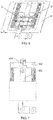
- Fig. 3 shows a schematic diagram of a power module according to an embodiment of the present disclosure.
- Fig. 4 shows a schematic diagram of a connector according to an embodiment of the present disclosure.
- Fig. 5 is a schematic diagram of mounting a group of switch elements on a base substrate according to an embodiment of the present disclosure.
- the power module includes a group 2 of switch elements, a molding part 7 and a connector 4.
- the group 2 of switch elements includes at least one pair of switch elements (three pairs 21, 22 and 23 of switch elements are shown). The present disclosure does not limit the number of pairs of switch elements.
- the molding part 7 is configured to package the group 2 of switch elements.
- the connector 4 includes a signal terminal 403 and a power terminal.
- the signal terminal 403 is electrically connected to the signal end of the group 2 of switch elements and fanned out from the molding part 7.
- the power terminal is electrically connected to the power end of the group 2 of switch elements, and fanned out from the molding part 7.
- the power terminal includes a positive power terminal 405, a negative power terminal 402 and an output power terminal 406.
- the positive power terminal 405 and the negative power terminal 402 are a first metal layer and a second metal layer, respectively.
- the first metal layer and the second metal layer are partially or completely stacked, and an insulating layer 408 is disposed between the first metal layer and the second metal layer to ensure electrical insulation between the positive power terminal 405 and the negative power terminal 402.
- the loop inductance of the power module can be effectively cancelled, thereby reducing the parasitic inductance of the power module and meeting the requirement of low inductance.
- multiple signal terminals 403 which can be configured to transmit signals from inside of the module to outside of the module, for example, transmitting parameter information such as current, voltage and temperature, sampled in the power module to outside of the module.
- the multiple signal terminals 403 can be configured to receive signals from outside of the module to apply in the module, for example, receiving a control signal from outside of the module to control switching on or off of the switch element inside of the module, and so on.
- the positive power terminals 405 and the negative power terminals 402 have protrusions 409 and 410 on the left and right sides respectively.
- the power module further includes a base substrate 1.
- the group 2 of switch elements is mounted on the base substrate 1, and the group 2 of switch elements and the base substrate 1 are packaged together in the molding part 7.
- the power module may further include a top substrate 5.
- the group 2 of switch elements is disposed between the top substrate 5 and the base substrate 1, and the group 2 of switch element, the top substrate 5 and the base substrate 1 are molded together in the molding part 7.
- the base substrate 1 and the top substrate 5 may be a DBC substrate, a Cu substrate, an Al substrate, an Al-SiC substrate, or the like.
- the top substrate 5 and the base substrate 1 may be the same type of substrate or different type. It should be understood that the present disclosure does not limit whether to provide the top substrate.
- the positive power terminal 405 and the negative power terminal 402 are fanned out from a first side of the molding part 7, and the signal terminal 403 and the output power terminal 406 are fanned out from a second side of the molding part 7.
- the first side is opposite to the second side. It should be understood that the positions where the signal terminal 403, the positive power terminal 405, the negative power terminal 402, and the output power terminal 406 are fanned out can be adjusted as desired.
- a distance between the first metal layer and the second metal layer is not more than 0.5 mm, which facilitates effective cancellation of the loop inductance.
- the switch element in the group 2 of switch elements may be an IGBT, a MOSFET or a transistor.
- the disclosure is not limited thereto.
- the pair 21, 22 or 23 of switch elements includes a first switch element S1 and a second switch element S2, the circuit connection topology of which is shown in Fig. 1 .
- the first switch element S1 includes a first end, a second end and a third end.
- the second switch element S2 includes a fourth end, a fifth end and a sixth end.
- the second end and the fourth end are electrically connected together as the power terminal O electrically connected to the output power terminal 406.
- the first end, as the power terminal P is electrically connected to the positive power terminal 405.
- the fifth end, as the power terminal N is electrically connected to the negative power terminal 402.
- the third end and the sixth end, as signal ends, are electrically connected to the signal terminal 403.
- the group 2 of switch elements includes a plurality of pairs of switch elements
- the plurality of pairs of switch elements are connected in parallel with each other. That is, the positive power end of one pair of switch elements and the positive power end of the other pair of switch elements are electrically connected.
- the negative power terminal of one pair of switch elements is electrically connected to the negative power terminal of the other pair of switch elements.
- the output power end of one pair of switch elements is electrically connected to the output power end of the other pair of switch elements.
- Fig. 6 is a schematic diagram of mounting a group of switch elements to a connector according to an embodiment of the present disclosure, which differs from Fig. 5 in that the group 2 of switch elements is directly mounted on the connector 4 instead of mounting the group 2 of switch elements on the base substrate 1. This solution can eliminate the cost of the base substrate and reduce the cost of the power module.
- the switch elements in the group 2 may be mounted to the positive power terminal 405 or the negative power terminal 402.
- Fig. 7 is a schematic diagram showing positioning dimensions of a power module according to an embodiment of the present disclosure.
- the connector in the power module includes a lead-frame 492 with a signal terminal and a bus-bar 491 as a power terminal.
- the lead-frame 492 is provided with a molding positioning hole 493. If the power module of the present disclosure is fabricated by the method shown in Fig. 2 , the lead-frame 492 and the bus-bar 491 are respectively assembled with the substrate.
- the tolerance m of the distance between the assembled molding positioning hole 493 and the bus-bar 491 is ⁇ 200um.
- the tolerance n of the body size of the bus-bar 491 is ⁇ 10um.
- the profiling mold-die for molding requires that the tolerance m of the distance between the molding positioning hole 493 and the bus-bar 491 is generally ⁇ 30um.
- the tolerance n of the body size of the bus-bar 491 is generally ⁇ 10um.
- the present disclosure provides a manufacturing method of a power module, which integrates a signal terminal, a power terminal and a connecting portion into an integral connector to meet the positioning accuracy requirement and complete the package.
- the method for manufacturing the power module of the present disclosure will be described in detail below with reference to the accompanying drawings.
- Fig. 8 illustrates a flowchart of a manufacturing method of a power module according to an embodiment of the present disclosure. As shown in Fig. 8 , the manufacturing method includes the following steps.
- a group 2 of switch elements is provided, the group of switch elements including at least one pair of switch elements.
- a base substrate 1 is provided, and the group 2 of switch elements is mounted on the base substrate 1.
- a connector 4 is provided.
- the connector includes a signal terminal 403, a power terminal and a connecting portion 401.
- the power terminal includes a positive power terminal 405, a negative power terminal 402 and an output power terminal 406.
- the connecting portion 401 connects the signal terminal 403, the positive power terminal 405, the negative power terminal 402 and the output power terminal 406 together.
- the positive power terminal 405 and the negative power terminal 402 are a first metal layer and a second metal layer, respectively.
- the first metal layer and the second metal layer are at least partially stacked.
- An insulating layer 408 is disposed between the first metal layer and the second metal layer.
- the connector 4 is electrically connected to the group 2 of switch elements.
- the signal terminal 403 is electrically connected to the signal end of the group 2 of switch elements, and the power terminal is electrically connected to the power end of the group 2 of switch elements.
- a top substrate 5 is provided. Providing the top substrate 5 is an optional step that can be skipped to directly perform the next step.
- a molding part 7 is provided to mold the group 2 of switch elements, and the signal terminal 403 and the power terminal are fanned out from the molding part 7.
- the group 2 of switch elements may be first connected to the base substrate 1 and then be performed with wire bonding.
- the connection may be in the form of soldering or silver sintering, or the like.
- the group 2 of switch elements includes at least one pair of switch elements.
- the switch element may be an IGBT, a MOSFET, a transistor or the like.
- the base substrate 1 may be a DBC substrate, a Cu substrate, an AI substrate, an Al- SiC substrate or the like.
- the wire bonding is to bond the signal terminal 403 of the chip to the base substrate 1 through a bonding wire.
- the bonding wire 3 may be an aluminum wire, a copper wire, a gold wire, a copper-aluminum composite wire or the like.
- Fig. 9 is a schematic diagram of a molding process in a manufacturing method of a power module according to an embodiment of the present disclosure.
- a mold-die 6 for the molding process in step S105 is composed of two parts, i.e. an upper mold cavity 61 and a lower mold cavity 62.
- a positioning pin 63 on the lower mold cavity 62 is positioned and assembled with the molding positioning hole 404 on the connector 4.
- a hollowed portion 64 of the mold-die 6 is matched with the module to be molded.
- the upper mold cavity 61 and the lower mold cavity 62 are closed together and then molded.
- the molding part 7 is made of a conventional EMC (Epoxy Molding Compound), or additionally adding with a silicone component, and filler used for molding may be selected from alumina, silica, aluminum nitride or the like.
- the connector 4 may be manufactured in a different manner.
- Fig. 10 is a schematic diagram of manufacturing a connector according to an embodiment of the present disclosure. As shown in Figs. 8 and 10 , the manufacturing method of the connector 4 includes: forming a signal terminal 403, a negative power terminal 402, an output power terminal 406, and a connecting portion 401 from a single piece of metal; providing a positive power terminal 405; a pre-trim insulating material film or insulating fluid material 91 is disposed between the positive power terminal 405 and the negative power terminal 402, and forming the connector 4.
- each part of the connector 4 can be prepared by machining, stamping, etching or the like. After the preparation of the metal layer is completed, a pre-trim insulating material film or insulating fluid material 91 is placed between adjacent two layers of metal. Finally, the metal portion of the connector 4 and the insulating material are subjected to high-temperature hot pressing with a mold-die 8.
- the mold-die 8 includes an upper mold part 81 and a lower mold part 82.
- the lower mold part 82 includes a positioning pin 83 matching the molding positioning hole 404 on the connector 4, to finally complete production of the connector 4.
- Fig. 11 is a schematic diagram showing the dimensions of a connector made according to Fig. 10 .
- the processing precision of the hot pressing mold-die 8 is generally ⁇ 5 um
- the processing precision of the metal portion of the connector 4 is generally ⁇ 10 um
- the tolerance g of a distance between the molding positioning hole 404 and the to-be-profiled portion 407 of the connector 4 can be controlled within ⁇ 30 um
- the tolerance h of the body size of the to-be-profiled portion 407 can be controlled within ⁇ 10 um.
- step S106 the molded power module is to be trimmed.
- Fig. 12 is a schematic diagram of a position to be trimmed on the connector made according to Fig. 10 .
- Fig. 13 is a schematic diagram showing the power module after the connector made according to Fig. 10 has been trimmed.
- Fig. 14 is an enlarged cross-sectional view of the power module along the A-A' direction of Fig. 13 .
- the connector 4 is to be pressed by pressing blocks 101, 102 of the trimming mold; then the trim blade is used to trim along the positions 103, 104 beside the pressing blocks.
- the trimmed metal elements 409 and 410 protrude from the other metal layer and the insulating material 411 to form protrusions.
- Fig. 15 is a schematic diagram of manufacturing a connector according to another embodiment of the present disclosure.
- the manufacturing method of the connector 4 includes: separately preparing at least a part of a signal terminal, a negative power terminal 418, an output power terminal 416 and a connecting portion; providing a positive power terminal 413; and providing a pre-trim insulating material film or insulating fluid material 92 between the positive power terminal 413 and the negative power terminal 418, to form the connector 4.
- the connector 4 includes components 413, 414, 416, 417, 418, which may each be a pre-formed, separate component. At least one component, such as the component 414, is provided with a molding positioning hole 415. Each component may be prepared by machining, stamping, etching or the like. After the various components are prepared, a pre-trim insulating material film or insulating fluid material 92 is disposed between adjacent two layers of metal. Finally, the metal portion of the connector 4 and the insulating portion are subjected to high-temperature hot pressing with a mold-die 8.
- the mold-die 8 includes an upper mold part 85 and a lower mold part 84.
- the lower mold part 84 includes a positioning pin 86 matching with the molding positioning hole 404, to finally complete the production of the connector 4.
- Fig. 16 is a schematic diagram showing the dimensions of the connector made according to Fig. 15 .
- the processing precision of the hot pressing mold-die 8 is generally ⁇ 5 um
- the processing precision of the metal portion of the connector 4 is generally ⁇ 10 um
- the tolerance i of a distance between the molding positioning hole 415 and the to-be-profiled position 419 of the connector 4 can be controlled within ⁇ 30 um
- the tolerance j of the body size of the to-be-profiled position 419 can be controlled within ⁇ 10 um.
- step S106 the molded power module is to be trimmed.
- Fig. 17 is a schematic diagram of a position to be trimmed on the connector made according to Fig. 15 .
- Fig. 18 is a schematic diagram of a power module and a projection of the connector made according to Fig. 15 .
- the connector 4 is to be pressed by the pressing blocks 105, 106 of the trimming mold. Then, the trim blade is used to trim along the positions 107, 108 or the positions 109, 110 beside the pressing blocks.
- the trimming positions are the positions 107, 108 on the insulating material, the trimmed insulating materials 420 and 421 protrude from the other metal layer and the insulating material 424 to form protrusions. If the trimming positions are the positions 109, 110 on the metal material, the trimmed metal materials 422 and 423 protrude from the other metal layer and the insulating material 424 to form protrusions.
- Fig. 19 is a flowchart of a manufacturing method of a power module according to another embodiment of the present disclosure. As shown in Fig. 19 , the manufacturing method includes the following steps.
- a group of switch elements is provided, the group of switch elements including at least one pair of switch elements.
- a connector including a signal terminal, a power terminal and a connection portion.
- the power terminal includes a positive power terminal, a negative power terminal and an output power terminal.
- the connection portion connects the signal terminal, the positive power terminal, the negative power terminal and the output power terminal together.
- the positive power terminal and the negative power terminal are respectively a first metal layer and a second metal layer which are at least partially stacked.
- An insulating layer is disposed between the first metal layer and the second metal layer.
- the group of switch elements is mounted on the connector.
- the connector is electrically connected to the group of switch elements.
- the signal terminal is electrically connected to the signal end of the group of switch elements, and the power terminal is electrically connected to the power end of the group of switch elements.
- a molding part is provided, to package the group of switch elements, and the signal terminal and the power terminal are fanned out from the molding part.
- the group of switch elements may be on the connector through soldering, silver sintering or the like.
- the signal end and the power end of the group of switch elements are connected to the signal terminal and the power terminal of the connector.
- the signal terminal can be connected through a bonding wire
- the power terminal can be connected through the bonding wire 3, or may be bridged by a metal material.
- the connection with the metal material may be welding, silver sintering or the like.
- the bonding wire may be an aluminum wire, a copper wire, a gold wire, a copper-aluminum composite wire or the like.
- this embodiment is different in that the group of switch elements is directly mounted on the connector instead of being mounted on the base substrate.
- Other related features regarding the group of switch elements, the connector, the molding, the trimming and the like may be the same as or similar to the embodiment shown in Fig. 8 , and will not be repeated herein. In this way, the cost of the base substrate can be eliminated and the cost for the power module can be reduced.
- the group of switch elements may be mounted to the positive power terminal or the negative power terminal of the connector according to specific demands.
- the power module according to some embodiments of the present disclosure can greatly reduce the parasitic inductance of the power module by stacking the positive power terminal and the negative power terminal.
- the tolerance of the distance between the molding positioning hole and the power terminal can be controlled within ⁇ 30 um, and the tolerance of the body size of the terminal can be controlled within ⁇ 10um, which can meet the package requirements and facilitate production.
Landscapes
- Inverter Devices (AREA)
- Engineering & Computer Science (AREA)
- Manufacturing & Machinery (AREA)
Abstract
Description
- The present invention relates to the field of power electronics, and in particular to a power module and a manufacturing method thereof.
- In the field of power electronics technology, power modules have been widely used. Especially with the continuous increase of the power and the gradual decrease of the volume of the power supply, the modularization of the switching devices has become a development trend.
- In a conventional power module, multiple switch elements may be packaged into one integral, but signal terminals and power terminals are often fanned out with a single-layer lead-frame, which may cause a large parasitic inductance in the power module.
Fig. 1 shows a schematic diagram of a half bridge circuit topology. As shown inFig. 1 , the circuit includes two switch elements S1 and S2 connected in series, and a capacitor C connected in parallel with the series connection branch, in which P, O, N indicate three input/output power terminals. Then the circuit includes parasitic inductances L1 from P to S1, parasitic inductances L3, L4 between S1 and S2, and parasitic inductance L2 from S2 to N. The switch elements S1 and S2 are packaged in the same package structure to form a power module. When the power terminals are fanned out in a single layer, the parasitic inductance L1+L2+L3+L4 in the module can be generally large, and the existence of these parasitic inductances may greatly affect the switching characteristics of the switching devices S1 and S2, causing a large spike voltage on these switching devices, which may in turn affect the efficiency of the power module and fail to meet the application requirements. - Molding type power module package structure mainly includes a chip, a substrate, a bonding wire, a signal terminal, a power terminal, connecting material and molding compound. The raw material of the signal terminal and the power terminal is etched from the same piece of metal or a stamped lead-frame.
Fig. 2 is a flowchart of a manufacturing method of a power module. As shown inFig. 2 , the manufacturing method of the power module includes: a: assembling a chip and a lead-frame to a substrate; b: connecting the chip and the corresponding terminal of the lead-frame; c: molding; and d: trimming. As to the profiling mold-die for the molding, it is required that the tolerance of the distance between themolding positioning hole 4000 and theterminal 4001 should be about ±30 um, and the tolerance of the body size of theterminal 4001 is about ±10 um. However, when any change occurs in the package structure, the existing packaging process cannot meet the packaging requirements anymore. - Therefore, there is a demand for improvements in the power module and the manufacturing method thereof.
- According to a first aspect of the present invention, there is provided a manufacturing method of a power module, including: providing a group of switch elements, the group of switch elements including at least one pair of switch elements; providing a connector, wherein the connector includes a signal terminal, a power terminal, and a connecting portion, the power terminal includes a positive power terminal, a negative power terminal and an output power terminal, the connecting portion connects the signal terminal, the positive power terminal, the negative power terminal and the output power terminal together, the positive power terminal and the negative power terminal are respectively a first metal layer and a second metal layer, the first metal layer and the second metal layer are at least partially stacked, and an insulating layer is disposed between the first metal layer and the second metal layer; electrically connecting the connector to the group of switch elements, wherein the signal terminal is electrically connected to a signal end of the group of switch elements, and the power terminal is electrically connected to a power end of the group of switch elements; providing a molding part, packaging the group of switch elements and fanning out the signal terminal and the power terminal from the molding part; and trimming the connector.
- According to a particular embodiment, trimming the connector comprises: pressing the connecting portion with pressing blocks, and then trimming at positions beside the pressing blocks.
- According to a particular embodiment, the method further comprises:
providing a base substrate, before the connector is electrically connected to the group of switch elements, mounting the group of switch elements on the base substrate, and disposing the base substrate within the molding part. - According to a particular embodiment, the method comprises:
providing a top substrate, after the connector is electrically connected to the group of switch elements, disposing the group of switch elements between the top substrate and the base substrate, and disposing the top substrate within the molding part. - According to a particular embodiment, the method further comprises:
before the connector is electrically connected to the group of switch elements, mounting the group of switch elements to the connector. - According to a particular embodiment, the group of switch elements is mounted to the positive power terminal or the negative power terminal of the connector.
- According to a particular embodiment, the method further comprises:
providing a molding positioning hole on the connector, and fitting the molding positioning hole with the positioning pin of a mold to perform molding. - According to a particular embodiment, providing a connector comprises:
- forming the signal terminal, the negative power terminal, the output power terminal and the connecting portion from a single piece of metal, or forming at least a part of the signal terminal, the negative power terminal, the output terminal and the connecting portion separately;
- providing the positive power terminal; and
- disposing the insulating layer between the positive power terminal and the negative power terminal.
- According to a particular embodiment, providing a connector further comprises: subjecting the portions of the connector to hot pressing at a high temperature with a mold-die.
- According to a second aspect of the present invention, there is provided a power module, including: a group of switch elements, the group of switch elements including at least one pair of switch elements; a molding part packaging the group of switch elements; and a connector, including: a signal terminal electrically connected to the signal end of the group of switch elements and fanned out from the molding part, and a power terminal electrically connected to a power end of the group of switch elements and fanned out from the molding part, wherein the power terminal includes a positive power terminal, a negative power terminal and an output power terminal, the positive power terminal and the negative power terminal are respectively a first metal layer and a second metal layer, the first metal layer and the second metal layer are at least partially stacked, and an insulating layer is disposed between the first metal layer and the second metal layer.
- According to a particular embodiment, the positive power terminal and the negative power terminal have protrusions on the sides thereof.
- According to a particular embodiment, the power module further comprises a base substrate disposed in the molding part, wherein the group of switch elements is mounted on the base substrate.
- According to a particular embodiment, the power module further comprises a top substrate disposed in the molding part, wherein the group of switch elements is disposed between the top substrate and the base substrate.
- According to a particular embodiment, the group of switch elements is mounted on the connector.
- According to a particular embodiment, the group of switch elements is mounted on the positive power terminal or the negative power terminal of the connector.
- According to a particular embodiment, the positive power terminal and the negative power terminal are fanned out from a first side of the molding part, and the signal terminal and the output power terminal are fanned out from a second side opposite to the first side of the molding part.
- According to a particular embodiment, a distance between the first metal layer and the second metal layer is not more than 0.5 mm.
- According to a particular embodiment, the pair of switch elements comprises a first switch element and a second switch element, the first switch element comprising a first end, a second end, and a third end, the second switch element comprising a fourth end, a fifth end, and a sixth end, wherein the second end and the fourth end are electrically connected together as a power end electrically connected to the output power terminal, and wherein the first end, as a power end, is electrically connected to the positive power terminal, and wherein the fifth end, as a power end, is electrically connected to the negative power terminal, and wherein the third end and the sixth end, as signal ends, are electrically connected to the signal terminal.
- The above and other objects, features, and advantages of the present disclosure will become more apparent from the aspects of the embodiments.
- The accompanying drawings, which are incorporated in and constitute a part of this specification, illustrate embodiments consistent with the disclosure and, together with the description, serve to explain the principles of the disclosure. It is apparent that the drawings in the following description are only some of the embodiments of the present disclosure, and other drawings may be obtained from those skilled in the art without departing from the drawings.
-
Fig. 1 is a schematic diagram of a half bridge circuit topology; -
Fig. 2 is a flowchart of a manufacturing method of a power module; -
Fig. 3 is a schematic diagram of a power module according to an embodiment of the present disclosure; -
Fig. 4 is a schematic diagram of a connector according to an embodiment of the present disclosure; -
Fig. 5 is a schematic diagram of mounting a group of switch elements on a base substrate according to an embodiment of the present disclosure; -
Fig. 6 is a schematic diagram of mounting a group of switch elements to a connector according to an embodiment of the present disclosure; -
Fig. 7 is a schematic diagram showing positioning dimensions of a power module according to an embodiment of the present disclosure; -
Fig. 8 is a flowchart of a manufacturing method of a power module according to an embodiment of the present disclosure; -
Fig. 9 is a schematic diagram of a molding process in a manufacturing method of a power module according to an embodiment of the present disclosure; -
Fig. 10 is a schematic diagram of manufacturing a connector according to an embodiment of the present disclosure; -
Fig. 11 is a schematic diagram showing the dimensions of a connector made according toFig. 10 ; -
Fig. 12 is a schematic diagram of a position to be trimmed on the connector made according toFig. 10 ; -
Fig. 13 is a schematic diagram showing the power module after the connector made according toFig. 10 has been trimmed; -
Fig. 14 is an enlarged cross-sectional view of the power module along the A-A' direction ofFig. 13 ; -
Fig. 15 is a schematic diagram of manufacturing a connector according to another embodiment of the present disclosure; -
Fig. 16 is a schematic diagram showing the dimensions of the connector made according toFig. 15 ; -
Fig. 17 is a schematic diagram of a position to be trimmed on the connector made according toFig. 15 ; -
Fig. 18 is a schematic diagram of a power module and a projection of the connector made according toFig. 15 ; and -
Fig. 19 is a flowchart of a manufacturing method of a power module according to another embodiment of the present disclosure. - Example embodiments will now be described more fully with reference to the accompanying drawings. The example embodiments can be embodied in a variety of forms, and should not be construed as being limited to the examples set forth herein; the described features, structures, or characteristics may be combined in any suitable manner in one or more embodiments. In the following description, numerous specific details are set forth However, one skilled in the art will appreciate that one or more of the specific details may be omitted or other methods, components, devices, steps, etc. may be employed.
- It should be noted that in the drawings, the dimensions of layers and regions may be exaggerated for clarity of illustration. It may also be understood that when an element or layer is referred to as "on" another element or layer, it may be directly on the other element or an intermediate layer may be present. In addition, it can be understood that when an element or layer is referred to as being "under" another element or layer, it may be directly under the other element or may have more than one intermediate layer or element. In addition, it can also be understood that when a layer or element is referred to as being "between" two layers or two elements, it can be a single layer between the two layers or the two elements, or more than one intermediate layer or element be present. Like reference numerals indicate like elements throughout.
- The present disclosure provides a power module and a manufacturing method thereof. The power module includes a group of switch elements including at least one pair of switch elements; a molding part for packaging the group of switch elements; and a connector, including a signal terminal, electrically connected to the signal end of the group of switch elements, and fanned out from the molding part, and a power terminal electrically connected to the power end of the group of switch elements and fanned out from the molding part. The power terminal includes a positive power terminal, a negative power terminal and an output power terminal. The positive power terminal and the negative power terminal are respectively a first metal layer and a second metal layer. The first metal layer and the second metal layer are at least partially stacked, and an insulating layer is disposed between the first metal layer and the second metal layer. By stacking the positive power terminal and the negative power terminal, the parasitic inductance of the power module can be greatly reduced. In addition, in the manufacture of the power module, by integrating the signal terminal, the power terminal and the connecting portion into an integral connector, the tolerance between the molding positioning hole and the power terminal can be ±30um, and the tolerance of the body size of the terminal can be ±10um, which can satisfy the package requirement and facilitate production.
-
Fig. 3 shows a schematic diagram of a power module according to an embodiment of the present disclosure.Fig. 4 shows a schematic diagram of a connector according to an embodiment of the present disclosure.Fig. 5 is a schematic diagram of mounting a group of switch elements on a base substrate according to an embodiment of the present disclosure. - As shown in
Figs. 3-5 , the power module includes agroup 2 of switch elements, a molding part 7 and aconnector 4. Thegroup 2 of switch elements includes at least one pair of switch elements (threepairs 21, 22 and 23 of switch elements are shown). The present disclosure does not limit the number of pairs of switch elements. The molding part 7 is configured to package thegroup 2 of switch elements. Theconnector 4 includes asignal terminal 403 and a power terminal. Thesignal terminal 403 is electrically connected to the signal end of thegroup 2 of switch elements and fanned out from the molding part 7. The power terminal is electrically connected to the power end of thegroup 2 of switch elements, and fanned out from the molding part 7. The power terminal includes apositive power terminal 405, anegative power terminal 402 and anoutput power terminal 406. Thepositive power terminal 405 and thenegative power terminal 402 are a first metal layer and a second metal layer, respectively. The first metal layer and the second metal layer are partially or completely stacked, and an insulatinglayer 408 is disposed between the first metal layer and the second metal layer to ensure electrical insulation between thepositive power terminal 405 and thenegative power terminal 402. - By providing the
positive power terminal 405 and thenegative power terminal 402 as partially or completely stacked metal layers, the loop inductance of the power module can be effectively cancelled, thereby reducing the parasitic inductance of the power module and meeting the requirement of low inductance. - It should be understood that there may be
multiple signal terminals 403, which can be configured to transmit signals from inside of the module to outside of the module, for example, transmitting parameter information such as current, voltage and temperature, sampled in the power module to outside of the module. Or, themultiple signal terminals 403 can be configured to receive signals from outside of the module to apply in the module, for example, receiving a control signal from outside of the module to control switching on or off of the switch element inside of the module, and so on. - According to an embodiment of the present disclosure, on the outside of the molding part 7, the
positive power terminals 405 and thenegative power terminals 402 haveprotrusions 409 and 410 on the left and right sides respectively. - According to an embodiment of the present disclosure, as shown in
Fig. 5 , the power module further includes a base substrate 1. Thegroup 2 of switch elements is mounted on the base substrate 1, and thegroup 2 of switch elements and the base substrate 1 are packaged together in the molding part 7. Further, the power module may further include a top substrate 5. Thegroup 2 of switch elements is disposed between the top substrate 5 and the base substrate 1, and thegroup 2 of switch element, the top substrate 5 and the base substrate 1 are molded together in the molding part 7. The base substrate 1 and the top substrate 5 may be a DBC substrate, a Cu substrate, an Al substrate, an Al-SiC substrate, or the like. The top substrate 5 and the base substrate 1 may be the same type of substrate or different type. It should be understood that the present disclosure does not limit whether to provide the top substrate. - According to an embodiment of the present disclosure, as shown in
Fig. 3 , thepositive power terminal 405 and thenegative power terminal 402 are fanned out from a first side of the molding part 7, and thesignal terminal 403 and theoutput power terminal 406 are fanned out from a second side of the molding part 7. The first side is opposite to the second side. It should be understood that the positions where thesignal terminal 403, thepositive power terminal 405, thenegative power terminal 402, and theoutput power terminal 406 are fanned out can be adjusted as desired. - According to an embodiment of the present disclosure, a distance between the first metal layer and the second metal layer is not more than 0.5 mm, which facilitates effective cancellation of the loop inductance.
- According to an embodiment of the present disclosure, the switch element in the
group 2 of switch elements may be an IGBT, a MOSFET or a transistor. However, the disclosure is not limited thereto. - According to an embodiment of the present disclosure, the
pair 21, 22 or 23 of switch elements includes a first switch element S1 and a second switch element S2, the circuit connection topology of which is shown inFig. 1 . The first switch element S1 includes a first end, a second end and a third end. The second switch element S2 includes a fourth end, a fifth end and a sixth end. The second end and the fourth end are electrically connected together as the power terminal O electrically connected to theoutput power terminal 406. The first end, as the power terminal P, is electrically connected to thepositive power terminal 405. The fifth end, as the power terminal N, is electrically connected to thenegative power terminal 402. The third end and the sixth end, as signal ends, are electrically connected to thesignal terminal 403. - It should be understood that when the
group 2 of switch elements includes a plurality of pairs of switch elements, the plurality of pairs of switch elements are connected in parallel with each other. That is, the positive power end of one pair of switch elements and the positive power end of the other pair of switch elements are electrically connected. The negative power terminal of one pair of switch elements is electrically connected to the negative power terminal of the other pair of switch elements. The output power end of one pair of switch elements is electrically connected to the output power end of the other pair of switch elements. -
Fig. 6 is a schematic diagram of mounting a group of switch elements to a connector according to an embodiment of the present disclosure, which differs fromFig. 5 in that thegroup 2 of switch elements is directly mounted on theconnector 4 instead of mounting thegroup 2 of switch elements on the base substrate 1. This solution can eliminate the cost of the base substrate and reduce the cost of the power module. - According to an embodiment of the present disclosure, the switch elements in the
group 2 may be mounted to thepositive power terminal 405 or thenegative power terminal 402. -
Fig. 7 is a schematic diagram showing positioning dimensions of a power module according to an embodiment of the present disclosure. As shown inFig. 7 , the connector in the power module includes a lead-frame 492 with a signal terminal and a bus-bar 491 as a power terminal. The lead-frame 492 is provided with amolding positioning hole 493. If the power module of the present disclosure is fabricated by the method shown inFig. 2 , the lead-frame 492 and the bus-bar 491 are respectively assembled with the substrate. The tolerance m of the distance between the assembledmolding positioning hole 493 and the bus-bar 491 is ±200um. The tolerance n of the body size of the bus-bar 491 is ±10um. The profiling mold-die for molding requires that the tolerance m of the distance between themolding positioning hole 493 and the bus-bar 491 is generally ±30um. The tolerance n of the body size of the bus-bar 491 is generally ±10um. Apparently, the conventional manufacturing method cannot meet the molding process requirements of the power module of the present disclosure and cannot be used for production. - To this end, the present disclosure provides a manufacturing method of a power module, which integrates a signal terminal, a power terminal and a connecting portion into an integral connector to meet the positioning accuracy requirement and complete the package. The method for manufacturing the power module of the present disclosure will be described in detail below with reference to the accompanying drawings.
-
Fig. 8 illustrates a flowchart of a manufacturing method of a power module according to an embodiment of the present disclosure. As shown inFig. 8 , the manufacturing method includes the following steps. - In S101, a
group 2 of switch elements is provided, the group of switch elements including at least one pair of switch elements. - In S102, a base substrate 1 is provided, and the
group 2 of switch elements is mounted on the base substrate 1. - In S103, a
connector 4 is provided. The connector includes asignal terminal 403, a power terminal and a connectingportion 401. The power terminal includes apositive power terminal 405, anegative power terminal 402 and anoutput power terminal 406. The connectingportion 401 connects thesignal terminal 403, thepositive power terminal 405, thenegative power terminal 402 and theoutput power terminal 406 together. Thepositive power terminal 405 and thenegative power terminal 402 are a first metal layer and a second metal layer, respectively. The first metal layer and the second metal layer are at least partially stacked. An insulatinglayer 408 is disposed between the first metal layer and the second metal layer. - In S104, the
connector 4 is electrically connected to thegroup 2 of switch elements. Thesignal terminal 403 is electrically connected to the signal end of thegroup 2 of switch elements, and the power terminal is electrically connected to the power end of thegroup 2 of switch elements. A top substrate 5 is provided. Providing the top substrate 5 is an optional step that can be skipped to directly perform the next step. - In S105, a molding part 7 is provided to mold the
group 2 of switch elements, and thesignal terminal 403 and the power terminal are fanned out from the molding part 7. - In S106, the
connector 4 is trimmed, to finally obtain the power module as shown inFig. 3 . - It should be noted that, in step S102, according to a specific implementation, the
group 2 of switch elements may be first connected to the base substrate 1 and then be performed with wire bonding. The connection may be in the form of soldering or silver sintering, or the like. Thegroup 2 of switch elements includes at least one pair of switch elements. The switch element may be an IGBT, a MOSFET, a transistor or the like. The base substrate 1 may be a DBC substrate, a Cu substrate, an AI substrate, an Al- SiC substrate or the like. The wire bonding is to bond thesignal terminal 403 of the chip to the base substrate 1 through a bonding wire. Thebonding wire 3 may be an aluminum wire, a copper wire, a gold wire, a copper-aluminum composite wire or the like. -
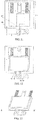
Fig. 9 is a schematic diagram of a molding process in a manufacturing method of a power module according to an embodiment of the present disclosure. As shown inFigs. 8 and9 , a mold-die 6 for the molding process in step S105 is composed of two parts, i.e. anupper mold cavity 61 and alower mold cavity 62. Apositioning pin 63 on thelower mold cavity 62 is positioned and assembled with themolding positioning hole 404 on theconnector 4. A hollowedportion 64 of the mold-die 6 is matched with the module to be molded. Theupper mold cavity 61 and thelower mold cavity 62 are closed together and then molded. The molding part 7 is made of a conventional EMC (Epoxy Molding Compound), or additionally adding with a silicone component, and filler used for molding may be selected from alumina, silica, aluminum nitride or the like. - In step S103, the
connector 4 may be manufactured in a different manner.Fig. 10 is a schematic diagram of manufacturing a connector according to an embodiment of the present disclosure. As shown inFigs. 8 and10 , the manufacturing method of theconnector 4 includes: forming asignal terminal 403, anegative power terminal 402, anoutput power terminal 406, and a connectingportion 401 from a single piece of metal; providing apositive power terminal 405; a pre-trim insulating material film or insulatingfluid material 91 is disposed between thepositive power terminal 405 and thenegative power terminal 402, and forming theconnector 4. - Specifically, each part of the
connector 4 can be prepared by machining, stamping, etching or the like. After the preparation of the metal layer is completed, a pre-trim insulating material film or insulatingfluid material 91 is placed between adjacent two layers of metal. Finally, the metal portion of theconnector 4 and the insulating material are subjected to high-temperature hot pressing with a mold-die 8. The mold-die 8 includes anupper mold part 81 and alower mold part 82. Thelower mold part 82 includes apositioning pin 83 matching themolding positioning hole 404 on theconnector 4, to finally complete production of theconnector 4. -
Fig. 11 is a schematic diagram showing the dimensions of a connector made according toFig. 10 . As shown inFig. 11 , since the processing precision of the hot pressing mold-die 8 is generally ±5 um, and the processing precision of the metal portion of theconnector 4 is generally ±10 um, after the hot pressing, the tolerance g of a distance between themolding positioning hole 404 and the to-be-profiled portion 407 of theconnector 4 can be controlled within ±30 um, and the tolerance h of the body size of the to-be-profiled portion 407 can be controlled within ±10 um. - In step S106, the molded power module is to be trimmed.
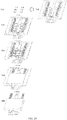
Fig. 12 is a schematic diagram of a position to be trimmed on the connector made according toFig. 10 .Fig. 13 is a schematic diagram showing the power module after the connector made according toFig. 10 has been trimmed.Fig. 14 is an enlarged cross-sectional view of the power module along the A-A' direction ofFig. 13 . As shown inFigs. 12-14 , in the trimming process, firstly, theconnector 4 is to be pressed by pressingblocks positions metal elements 409 and 410 protrude from the other metal layer and the insulatingmaterial 411 to form protrusions. -
Fig. 15 is a schematic diagram of manufacturing a connector according to another embodiment of the present disclosure. As shown inFig. 15 , the manufacturing method of theconnector 4 includes: separately preparing at least a part of a signal terminal, anegative power terminal 418, anoutput power terminal 416 and a connecting portion; providing apositive power terminal 413; and providing a pre-trim insulating material film or insulatingfluid material 92 between thepositive power terminal 413 and thenegative power terminal 418, to form theconnector 4. - Specifically, the
connector 4 includescomponents component 414, is provided with amolding positioning hole 415. Each component may be prepared by machining, stamping, etching or the like. After the various components are prepared, a pre-trim insulating material film or insulatingfluid material 92 is disposed between adjacent two layers of metal. Finally, the metal portion of theconnector 4 and the insulating portion are subjected to high-temperature hot pressing with a mold-die 8. The mold-die 8 includes anupper mold part 85 and alower mold part 84. Thelower mold part 84 includes apositioning pin 86 matching with themolding positioning hole 404, to finally complete the production of theconnector 4. -
Fig. 16 is a schematic diagram showing the dimensions of the connector made according toFig. 15 . As shown inFig. 16 , since the processing precision of the hot pressing mold-die 8 is generally ±5 um, and the processing precision of the metal portion of theconnector 4 is generally ±10 um, after the hot pressing, the tolerance i of a distance between themolding positioning hole 415 and the to-be-profiled position 419 of theconnector 4 can be controlled within ±30 um, and the tolerance j of the body size of the to-be-profiled position 419 can be controlled within ±10 um. - In step S106, the molded power module is to be trimmed.
Fig. 17 is a schematic diagram of a position to be trimmed on the connector made according toFig. 15 .Fig. 18 is a schematic diagram of a power module and a projection of the connector made according toFig. 15 . As shown inFigs. 17 and 18 , in the trimming process, theconnector 4 is to be pressed by thepressing blocks positions positions positions materials material 424 to form protrusions. If the trimming positions are thepositions metal materials material 424 to form protrusions. - In the above embodiments, the switch elements are all placed or mounted on the base substrate. In other embodiments, the power module may also be a structure without a base substrate, such as the group of switch elements being directly mounted on the connector.
Fig. 19 is a flowchart of a manufacturing method of a power module according to another embodiment of the present disclosure. As shown inFig. 19 , the manufacturing method includes the following steps. - In S201, a group of switch elements is provided, the group of switch elements including at least one pair of switch elements.
- In S202, a connector is provided, the connector including a signal terminal, a power terminal and a connection portion. The power terminal includes a positive power terminal, a negative power terminal and an output power terminal. The connection portion connects the signal terminal, the positive power terminal, the negative power terminal and the output power terminal together. The positive power terminal and the negative power terminal are respectively a first metal layer and a second metal layer which are at least partially stacked. An insulating layer is disposed between the first metal layer and the second metal layer.
- In S203, the group of switch elements is mounted on the connector.
- In S204, the connector is electrically connected to the group of switch elements. The signal terminal is electrically connected to the signal end of the group of switch elements, and the power terminal is electrically connected to the power end of the group of switch elements.
- In S205, a molding part is provided, to package the group of switch elements, and the signal terminal and the power terminal are fanned out from the molding part.
- In S206, the connector is trimmed, to finally obtain the power module as shown in
Fig. 3 . - It should be noted that, in step S203, the group of switch elements may be on the connector through soldering, silver sintering or the like. In step S204, the signal end and the power end of the group of switch elements are connected to the signal terminal and the power terminal of the connector. Wherein the signal terminal can be connected through a bonding wire, and the power terminal can be connected through the
bonding wire 3, or may be bridged by a metal material. The connection with the metal material may be welding, silver sintering or the like. The bonding wire may be an aluminum wire, a copper wire, a gold wire, a copper-aluminum composite wire or the like. - Compared with the embodiment shown in
Fig. 8 , this embodiment is different in that the group of switch elements is directly mounted on the connector instead of being mounted on the base substrate. Other related features regarding the group of switch elements, the connector, the molding, the trimming and the like may be the same as or similar to the embodiment shown inFig. 8 , and will not be repeated herein. In this way, the cost of the base substrate can be eliminated and the cost for the power module can be reduced. - According to an embodiment of the present disclosure, the group of switch elements may be mounted to the positive power terminal or the negative power terminal of the connector according to specific demands.
- From the above detailed description, those skilled in the art will readily appreciate that a power module and a manufacturing method thereof according to embodiments of the present disclosure have one or more of the following advantages.
- The power module according to some embodiments of the present disclosure can greatly reduce the parasitic inductance of the power module by stacking the positive power terminal and the negative power terminal.
- According to the manufacturing method of the power module according to some embodiments of the present disclosure, by integrating the signal terminal, the power terminal and the connecting portion into an integral connector, the tolerance of the distance between the molding positioning hole and the power terminal can be controlled within ±30 um, and the tolerance of the body size of the terminal can be controlled within ±10um, which can meet the package requirements and facilitate production.
- Other embodiments of the disclosure will be apparent to those skilled in the art from consideration of the specification and practice of the disclosure disclosed here. This application is intended to cover any variations, uses, or adaptations of the disclosure following the general principles thereof and including such departures from the present disclosure as come within known or customary practice in the art. It is intended that the specification and examples be considered as exemplary only, with a true scope of the disclosure being indicated by the following claims.
- It will be appreciated that the present disclosure is not limited to the exact construction that has been described above and illustrated in the accompanying drawings, and that various modifications and changes may be made without departing from the scope thereof. It is intended that the scope of the disclosure only be limited by the appended claims.
Claims (18)
- A manufacturing method of a power module, comprising:providing (S101) a group (2) of switch elements, the group of switch elements comprising at least one pair of switch elements;providing (S103) a connector (4), the connector (4) comprising a signal terminal (403), a power terminal and a connecting portion (401), wherein the power terminal comprises a positive power terminal (405), a negative power terminal (402) and an output power terminal (406), the connecting portion (401) connects the signal terminal (403), the positive power terminal (405), the negative power terminal (402) and the output power terminal (406) together, and wherein the positive power terminal (405) and the negative power terminal (402) are respectively a first metal layer and a second metal layer, the first metal layer and the second metal layer being at least partially stacked, with an insulating layer (408) disposed between the first metal layer and the second metal layer;electrically connecting (S104) the connector (4) to the group (2) of switch elements, wherein the signal terminal (403) is electrically connected to a signal end of the group (2) of switch elements, and the power terminal is electrically connected to a power end of the group (2) of switch elements;providing (S105) a molding part (7), packaging the group (2) of switch elements and fanning out the signal terminal (403) and the power terminal from the molding part (7); andtrimming (S106) the connector (4).
- The manufacturing method according to claim 1, wherein trimming (S106) the connector (4) comprises: pressing the connecting portion (401) with pressing blocks (101, 102), and then trimming at positions (103, 104) beside the pressing blocks (101, 102).
- The manufacturing method according to claim 1, further comprising:
providing (S102) a base substrate (1), before the connector (4) is electrically connected to the group (2) of switch elements, mounting the group (2) of switch elements on the base substrate (1), and disposing the base substrate (1) within the molding part (7). - The manufacturing method according to claim 3, further comprising:
providing a top substrate (5), after the connector (4) is electrically connected to the group (2) of switch elements, disposing the group (2) of switch elements between the top substrate (5) and the base substrate (1), and disposing the top substrate (5) within the molding part (7). - The manufacturing method according to claim 1, further comprising:
before the connector (4) is electrically connected to the group (2) of switch elements, mounting the group (2) of switch elements to the connector (4). - The manufacturing method according to claim 5, wherein the group (2) of switch elements is mounted to the positive power terminal (405) or the negative power terminal (402) of the connector (4).
- The manufacturing method according to claim 1, further comprising:
providing a molding positioning hole (4000) on the connector (4), and fitting the molding positioning hole (4000) with the positioning pin (63) of a mold to perform molding. - The manufacturing method according to claim 1, wherein providing (S103) a connector (4) comprises:forming the signal terminal (403), the negative power terminal (402), the output power terminal (406) and the connecting portion (401) from a single piece of metal, or forming at least a part of the signal terminal (403), the negative power terminal (402), the output terminal (406) and the connecting portion (401) separately;providing the positive power terminal (405); anddisposing the insulating layer (408) between the positive power terminal (405) and the negative power terminal (402).
- The manufacturing method according to claim 8, wherein providing a connector (4) further comprises: subjecting the portions of the connector (4) to hot pressing at a high temperature with a mold-die (6).
- A power module, comprising:a group (2) of switch elements, comprising at least one pair of switch elements;a molding part (7), packaging the group (2) of switch elements; anda connector (4), comprising:a signal terminal (403) electrically connected to the signal end of the group (2) of switch elements and fanned out from the molding part (7); anda power terminal electrically connected to a power end of the group (2) of switch elements and fanned out from the molding part (7), wherein the power terminal comprises a positive power terminal (405), a negative power terminal (402) and an output power terminal (406), the positive power terminal (405) and the negative power terminal (402) are respectively a first metal layer and a second metal layer, the first metal layer and the second metal layer are at least partially stacked, and an insulating layer (408) is disposed between the first metal layer and the second metal layer.
- The power module according to claim 10, wherein the positive power terminal (405) and the negative power terminal (402) have protrusions on the sides thereof.
- The power module according to claim 10, further comprising a base substrate disposed in the molding part (7), wherein the group (2) of switch elements is mounted on the base substrate.
- The power module according to claim 12, further comprising a top substrate (5) disposed in the molding part (7), wherein the group (2) of switch elements is disposed between the top substrate (5) and the base substrate (1).
- The power module according to claim 10, wherein the group (2) of switch elements is mounted on the connector (4).
- The power module according to claim 14, wherein the group (2) of switch elements is mounted on the positive power terminal (405) or the negative power terminal (402) of the connector (4).
- The power module according to claim 10, wherein the positive power terminal (405) and the negative power terminal (402) are fanned out from a first side of the molding part (7), and the signal terminal (403) and the output power terminal (406) are fanned out from a second side opposite to the first side of the molding part (7).
- The power module according to claim 10, wherein a distance between the first metal layer and the second metal layer is not more than 0.5 mm.
- The power module according to claim 10, wherein the pair (21, 22, 23) of switch elements comprises a first switch element (S1) and a second switch element (S2), the first switch element (S1) comprising a first end, a second end, and a third end, the second switch element (S2) comprising a fourth end, a fifth end, and a sixth end, wherein the second end and the fourth end are electrically connected together as a power end electrically connected to the output power terminal (406), and wherein the first end, as a power end, is electrically connected to the positive power terminal (405), and wherein the fifth end, as a power end, is electrically connected to the negative power terminal (402), and wherein the third end and the sixth end, as signal ends, are electrically connected to the signal terminal (403).
Applications Claiming Priority (1)
| Application Number | Priority Date | Filing Date | Title |
|---|---|---|---|
| CN201810270703.4A CN110323142B (en) | 2018-03-29 | 2018-03-29 | Power module and method of manufacturing the same |
Publications (2)
| Publication Number | Publication Date |
|---|---|
| EP3547365A1 true EP3547365A1 (en) | 2019-10-02 |
| EP3547365B1 EP3547365B1 (en) | 2021-03-24 |
Family
ID=65275945
Family Applications (1)
| Application Number | Title | Priority Date | Filing Date |
|---|---|---|---|
| EP19153904.8A Active EP3547365B1 (en) | 2018-03-29 | 2019-01-28 | Power module and manufacturing method thereof |
Country Status (4)
| Country | Link |
|---|---|
| US (1) | US10886200B2 (en) |
| EP (1) | EP3547365B1 (en) |
| JP (1) | JP6785893B2 (en) |
| CN (1) | CN110323142B (en) |
Cited By (1)
| Publication number | Priority date | Publication date | Assignee | Title |
|---|---|---|---|---|
| CN120581507A (en) * | 2025-08-04 | 2025-09-02 | 潍柴动力股份有限公司 | Power module |
Families Citing this family (7)
| Publication number | Priority date | Publication date | Assignee | Title |
|---|---|---|---|---|
| JP7221877B2 (en) * | 2017-04-28 | 2023-02-14 | ヒタチ・エナジー・スウィツァーランド・アクチェンゲゼルシャフト | Power supply modules based on normally-on semiconductor switches |
| CN112599505B (en) * | 2020-12-15 | 2025-03-25 | 华芯威半导体科技(北京)有限责任公司 | A low parasitic inductance power module |
| EP4040471B1 (en) * | 2021-02-08 | 2025-08-06 | Hitachi Energy Ltd | Power semiconductor module, power semiconductor device and method for producing a power semiconductor device |
| CN115534214B (en) * | 2022-08-31 | 2026-03-06 | 易纳纬(杭州)智能科技有限公司 | Manufacturing process of a motor main frame control system |
| CN118588695B (en) * | 2023-03-03 | 2026-05-05 | 比亚迪股份有限公司 | A method for manufacturing a power module and the power module itself. |
| CN117637500A (en) * | 2024-01-25 | 2024-03-01 | 广东芯聚能半导体有限公司 | Injection molding method for laminated terminals of power semiconductor modules |
| CN119108363A (en) * | 2024-08-12 | 2024-12-10 | 中国第一汽车股份有限公司 | Silicon carbide power module and method for manufacturing silicon carbide power module |
Citations (3)
| Publication number | Priority date | Publication date | Assignee | Title |
|---|---|---|---|---|
| EP1172908A2 (en) * | 2000-07-13 | 2002-01-16 | Nissan Motor Co., Ltd. | Structure of wiring connection |
| WO2014208450A1 (en) * | 2013-06-24 | 2014-12-31 | 日産自動車株式会社 | Electric power converter |
| EP2899757A1 (en) * | 2012-09-20 | 2015-07-29 | Rohm Co., Ltd. | Power module semiconductor device and inverter device, power module semiconductor device producing method, and mold |
Family Cites Families (13)
| Publication number | Priority date | Publication date | Assignee | Title |
|---|---|---|---|---|
| EP0000757B1 (en) * | 1977-08-08 | 1981-08-05 | Ciba-Geigy Ag | Process for the preparation of triarylphosphites |
| DE2739198C2 (en) * | 1977-08-31 | 1985-06-27 | Küppersbusch AG, 4650 Gelsenkirchen | Device for cooking food with hot air |
| JP5618595B2 (en) * | 2010-04-01 | 2014-11-05 | 日立オートモティブシステムズ株式会社 | Power module and power conversion device including power module |
| JP2013258387A (en) * | 2012-05-15 | 2013-12-26 | Rohm Co Ltd | Power-module semiconductor device |
| JP6295768B2 (en) * | 2014-03-26 | 2018-03-20 | 株式会社デンソー | Manufacturing method of semiconductor device |
| JP6152842B2 (en) * | 2014-11-04 | 2017-06-28 | トヨタ自動車株式会社 | Semiconductor device and manufacturing method thereof |
| JP6447914B2 (en) * | 2015-02-05 | 2019-01-09 | 株式会社 Acr | DC module wiring board for power module and manufacturing method thereof |
| JP6769707B2 (en) * | 2015-12-03 | 2020-10-14 | ローム株式会社 | Semiconductor module |
| CN108352380A (en) * | 2016-01-05 | 2018-07-31 | 日立汽车系统株式会社 | power semiconductor device |
| WO2017209191A1 (en) * | 2016-06-01 | 2017-12-07 | ローム株式会社 | Semiconductor power module |
| CN107170714B (en) | 2017-06-14 | 2020-01-14 | 扬州国扬电子有限公司 | Low parasitic inductance power module and double-sided heat dissipation low parasitic inductance power module |
| CN107369657B (en) * | 2017-08-30 | 2023-10-13 | 扬州国扬电子有限公司 | A double-sided cooling power module with multiple areas arranged side by side |
| CN107393901B (en) | 2017-08-30 | 2023-10-13 | 扬州国扬电子有限公司 | A double-sided cooling power module with laminated substrate |
-
2018
- 2018-03-29 CN CN201810270703.4A patent/CN110323142B/en active Active
-
2019
- 2019-01-21 JP JP2019007448A patent/JP6785893B2/en active Active
- 2019-01-28 US US16/258,747 patent/US10886200B2/en active Active
- 2019-01-28 EP EP19153904.8A patent/EP3547365B1/en active Active
Patent Citations (3)
| Publication number | Priority date | Publication date | Assignee | Title |
|---|---|---|---|---|
| EP1172908A2 (en) * | 2000-07-13 | 2002-01-16 | Nissan Motor Co., Ltd. | Structure of wiring connection |
| EP2899757A1 (en) * | 2012-09-20 | 2015-07-29 | Rohm Co., Ltd. | Power module semiconductor device and inverter device, power module semiconductor device producing method, and mold |
| WO2014208450A1 (en) * | 2013-06-24 | 2014-12-31 | 日産自動車株式会社 | Electric power converter |
Cited By (1)
| Publication number | Priority date | Publication date | Assignee | Title |
|---|---|---|---|---|
| CN120581507A (en) * | 2025-08-04 | 2025-09-02 | 潍柴动力股份有限公司 | Power module |
Also Published As
| Publication number | Publication date |
|---|---|
| JP2019176130A (en) | 2019-10-10 |
| JP6785893B2 (en) | 2020-11-18 |
| CN110323142B (en) | 2021-08-31 |
| EP3547365B1 (en) | 2021-03-24 |
| US20190304882A1 (en) | 2019-10-03 |
| US10886200B2 (en) | 2021-01-05 |
| CN110323142A (en) | 2019-10-11 |
Similar Documents
| Publication | Publication Date | Title |
|---|---|---|
| EP3547365B1 (en) | Power module and manufacturing method thereof | |
| US10685895B2 (en) | Power module with lead component and manufacturing method thereof | |
| US11239132B2 (en) | Semiconductor power device with corresponding package and related manufacturing process | |
| EP3226292B1 (en) | Lead frame, semiconductor device, method for manufacturing lead frame, and method for manufacturing semiconductor device | |
| EP1096566A2 (en) | Electronic part and method of assembling the same | |
| CN110783302B (en) | Semiconductor package having overlapping conductive regions and method of manufacturing the same | |
| US20110260314A1 (en) | Die package and corresponding method for realizing a double side cooling of a die package | |
| US3577633A (en) | Method of making a semiconductor device | |
| US20200303360A1 (en) | Semiconductor device | |
| JP2023549784A (en) | Packaged RF power equipment with PCB routing | |
| CN115702466B (en) | Leadframe capacitors | |
| CN103858228A (en) | Semiconductor device and method of manufacture thereof | |
| CN115206919A (en) | Semiconductor device with a plurality of semiconductor chips | |
| JP2014154770A (en) | Semiconductor device and semiconductor device manufacturing method | |
| US11694945B2 (en) | Lead frame package having conductive surfaces | |
| US20240332141A1 (en) | Semiconductor device package for press fit assembly | |
| US11302569B2 (en) | Method for manufacturing semiconductor device and semiconductor device | |
| US20250218914A1 (en) | Package with component-carrying intermediate structure and additional carrier having reference potential structure | |
| CN120527328A (en) | Lead frame assembly, power device packaging structure and preparation method thereof, and mold | |
| KR20250129767A (en) | Semiconductor package with upper heat spreader and lower flat | |
| WO2025162582A1 (en) | High power density low parasitic inductance sic half bridge module | |
| TW202510243A (en) | Package | |
| US20210210421A1 (en) | Power semiconductor module | |
| CN120674403A (en) | Semiconductor device and preparation method thereof | |
| JPH0831489B2 (en) | Method for manufacturing resin-sealed electric component |
Legal Events
| Date | Code | Title | Description |
|---|---|---|---|
| PUAI | Public reference made under article 153(3) epc to a published international application that has entered the european phase |
Free format text: ORIGINAL CODE: 0009012 |
|
| STAA | Information on the status of an ep patent application or granted ep patent |
Free format text: STATUS: REQUEST FOR EXAMINATION WAS MADE |
|
| 17P | Request for examination filed |
Effective date: 20190128 |
|
| AK | Designated contracting states |
Kind code of ref document: A1 Designated state(s): AL AT BE BG CH CY CZ DE DK EE ES FI FR GB GR HR HU IE IS IT LI LT LU LV MC MK MT NL NO PL PT RO RS SE SI SK SM TR |
|
| AX | Request for extension of the european patent |
Extension state: BA ME |
|
| RIN1 | Information on inventor provided before grant (corrected) |
Inventor name: HONG, SHOUYU Inventor name: ZHAO, ZHENQING Inventor name: XU, HAIBIN Inventor name: CHENG, WEI Inventor name: WANG, TAO |
|
| REG | Reference to a national code |
Ref country code: DE Ref legal event code: R079 Ref document number: 602019003300 Country of ref document: DE Free format text: PREVIOUS MAIN CLASS: H01L0025070000 Ipc: H01L0023495000 |
|
| RIC1 | Information provided on ipc code assigned before grant |
Ipc: H01L 25/07 20060101ALI20200827BHEP Ipc: H01L 23/48 20060101ALI20200827BHEP Ipc: H01L 25/00 20060101ALI20200827BHEP Ipc: H01L 23/495 20060101AFI20200827BHEP Ipc: H01L 25/18 20060101ALI20200827BHEP |
|
| GRAP | Despatch of communication of intention to grant a patent |
Free format text: ORIGINAL CODE: EPIDOSNIGR1 |
|
| STAA | Information on the status of an ep patent application or granted ep patent |
Free format text: STATUS: GRANT OF PATENT IS INTENDED |
|
| INTG | Intention to grant announced |
Effective date: 20201023 |
|
| GRAS | Grant fee paid |
Free format text: ORIGINAL CODE: EPIDOSNIGR3 |
|
| GRAA | (expected) grant |
Free format text: ORIGINAL CODE: 0009210 |
|
| STAA | Information on the status of an ep patent application or granted ep patent |
Free format text: STATUS: THE PATENT HAS BEEN GRANTED |
|
| AK | Designated contracting states |
Kind code of ref document: B1 Designated state(s): AL AT BE BG CH CY CZ DE DK EE ES FI FR GB GR HR HU IE IS IT LI LT LU LV MC MK MT NL NO PL PT RO RS SE SI SK SM TR |
|
| REG | Reference to a national code |
Ref country code: GB Ref legal event code: FG4D |
|
| REG | Reference to a national code |
Ref country code: CH Ref legal event code: EP |
|
| REG | Reference to a national code |
Ref country code: IE Ref legal event code: FG4D |
|
| REG | Reference to a national code |
Ref country code: DE Ref legal event code: R096 Ref document number: 602019003300 Country of ref document: DE Ref country code: AT Ref legal event code: REF Ref document number: 1375362 Country of ref document: AT Kind code of ref document: T Effective date: 20210415 |
|
| REG | Reference to a national code |
Ref country code: LT Ref legal event code: MG9D |
|
| PG25 | Lapsed in a contracting state [announced via postgrant information from national office to epo] |
Ref country code: NO Free format text: LAPSE BECAUSE OF FAILURE TO SUBMIT A TRANSLATION OF THE DESCRIPTION OR TO PAY THE FEE WITHIN THE PRESCRIBED TIME-LIMIT Effective date: 20210624 Ref country code: BG Free format text: LAPSE BECAUSE OF FAILURE TO SUBMIT A TRANSLATION OF THE DESCRIPTION OR TO PAY THE FEE WITHIN THE PRESCRIBED TIME-LIMIT Effective date: 20210624 Ref country code: HR Free format text: LAPSE BECAUSE OF FAILURE TO SUBMIT A TRANSLATION OF THE DESCRIPTION OR TO PAY THE FEE WITHIN THE PRESCRIBED TIME-LIMIT Effective date: 20210324 Ref country code: GR Free format text: LAPSE BECAUSE OF FAILURE TO SUBMIT A TRANSLATION OF THE DESCRIPTION OR TO PAY THE FEE WITHIN THE PRESCRIBED TIME-LIMIT Effective date: 20210625 Ref country code: FI Free format text: LAPSE BECAUSE OF FAILURE TO SUBMIT A TRANSLATION OF THE DESCRIPTION OR TO PAY THE FEE WITHIN THE PRESCRIBED TIME-LIMIT Effective date: 20210324 |
|
| PG25 | Lapsed in a contracting state [announced via postgrant information from national office to epo] |
Ref country code: SE Free format text: LAPSE BECAUSE OF FAILURE TO SUBMIT A TRANSLATION OF THE DESCRIPTION OR TO PAY THE FEE WITHIN THE PRESCRIBED TIME-LIMIT Effective date: 20210324 Ref country code: RS Free format text: LAPSE BECAUSE OF FAILURE TO SUBMIT A TRANSLATION OF THE DESCRIPTION OR TO PAY THE FEE WITHIN THE PRESCRIBED TIME-LIMIT Effective date: 20210324 Ref country code: LV Free format text: LAPSE BECAUSE OF FAILURE TO SUBMIT A TRANSLATION OF THE DESCRIPTION OR TO PAY THE FEE WITHIN THE PRESCRIBED TIME-LIMIT Effective date: 20210324 |
|
| REG | Reference to a national code |
Ref country code: NL Ref legal event code: MP Effective date: 20210324 |
|
| REG | Reference to a national code |
Ref country code: AT Ref legal event code: MK05 Ref document number: 1375362 Country of ref document: AT Kind code of ref document: T Effective date: 20210324 |
|
| PG25 | Lapsed in a contracting state [announced via postgrant information from national office to epo] |
Ref country code: NL Free format text: LAPSE BECAUSE OF FAILURE TO SUBMIT A TRANSLATION OF THE DESCRIPTION OR TO PAY THE FEE WITHIN THE PRESCRIBED TIME-LIMIT Effective date: 20210324 |
|
| PG25 | Lapsed in a contracting state [announced via postgrant information from national office to epo] |
Ref country code: SM Free format text: LAPSE BECAUSE OF FAILURE TO SUBMIT A TRANSLATION OF THE DESCRIPTION OR TO PAY THE FEE WITHIN THE PRESCRIBED TIME-LIMIT Effective date: 20210324 Ref country code: AT Free format text: LAPSE BECAUSE OF FAILURE TO SUBMIT A TRANSLATION OF THE DESCRIPTION OR TO PAY THE FEE WITHIN THE PRESCRIBED TIME-LIMIT Effective date: 20210324 Ref country code: EE Free format text: LAPSE BECAUSE OF FAILURE TO SUBMIT A TRANSLATION OF THE DESCRIPTION OR TO PAY THE FEE WITHIN THE PRESCRIBED TIME-LIMIT Effective date: 20210324 Ref country code: CZ Free format text: LAPSE BECAUSE OF FAILURE TO SUBMIT A TRANSLATION OF THE DESCRIPTION OR TO PAY THE FEE WITHIN THE PRESCRIBED TIME-LIMIT Effective date: 20210324 Ref country code: LT Free format text: LAPSE BECAUSE OF FAILURE TO SUBMIT A TRANSLATION OF THE DESCRIPTION OR TO PAY THE FEE WITHIN THE PRESCRIBED TIME-LIMIT Effective date: 20210324 |
|
| PG25 | Lapsed in a contracting state [announced via postgrant information from national office to epo] |
Ref country code: IS Free format text: LAPSE BECAUSE OF FAILURE TO SUBMIT A TRANSLATION OF THE DESCRIPTION OR TO PAY THE FEE WITHIN THE PRESCRIBED TIME-LIMIT Effective date: 20210724 Ref country code: PL Free format text: LAPSE BECAUSE OF FAILURE TO SUBMIT A TRANSLATION OF THE DESCRIPTION OR TO PAY THE FEE WITHIN THE PRESCRIBED TIME-LIMIT Effective date: 20210324 Ref country code: PT Free format text: LAPSE BECAUSE OF FAILURE TO SUBMIT A TRANSLATION OF THE DESCRIPTION OR TO PAY THE FEE WITHIN THE PRESCRIBED TIME-LIMIT Effective date: 20210726 Ref country code: RO Free format text: LAPSE BECAUSE OF FAILURE TO SUBMIT A TRANSLATION OF THE DESCRIPTION OR TO PAY THE FEE WITHIN THE PRESCRIBED TIME-LIMIT Effective date: 20210324 Ref country code: SK Free format text: LAPSE BECAUSE OF FAILURE TO SUBMIT A TRANSLATION OF THE DESCRIPTION OR TO PAY THE FEE WITHIN THE PRESCRIBED TIME-LIMIT Effective date: 20210324 |
|
| REG | Reference to a national code |
Ref country code: DE Ref legal event code: R097 Ref document number: 602019003300 Country of ref document: DE |
|
| PG25 | Lapsed in a contracting state [announced via postgrant information from national office to epo] |
Ref country code: ES Free format text: LAPSE BECAUSE OF FAILURE TO SUBMIT A TRANSLATION OF THE DESCRIPTION OR TO PAY THE FEE WITHIN THE PRESCRIBED TIME-LIMIT Effective date: 20210324 Ref country code: DK Free format text: LAPSE BECAUSE OF FAILURE TO SUBMIT A TRANSLATION OF THE DESCRIPTION OR TO PAY THE FEE WITHIN THE PRESCRIBED TIME-LIMIT Effective date: 20210324 Ref country code: AL Free format text: LAPSE BECAUSE OF FAILURE TO SUBMIT A TRANSLATION OF THE DESCRIPTION OR TO PAY THE FEE WITHIN THE PRESCRIBED TIME-LIMIT Effective date: 20210324 |
|
| PLBE | No opposition filed within time limit |
Free format text: ORIGINAL CODE: 0009261 |
|
| STAA | Information on the status of an ep patent application or granted ep patent |
Free format text: STATUS: NO OPPOSITION FILED WITHIN TIME LIMIT |
|
| PG25 | Lapsed in a contracting state [announced via postgrant information from national office to epo] |
Ref country code: SI Free format text: LAPSE BECAUSE OF FAILURE TO SUBMIT A TRANSLATION OF THE DESCRIPTION OR TO PAY THE FEE WITHIN THE PRESCRIBED TIME-LIMIT Effective date: 20210324 |
|
| 26N | No opposition filed |
Effective date: 20220104 |
|
| PG25 | Lapsed in a contracting state [announced via postgrant information from national office to epo] |
Ref country code: IS Free format text: LAPSE BECAUSE OF FAILURE TO SUBMIT A TRANSLATION OF THE DESCRIPTION OR TO PAY THE FEE WITHIN THE PRESCRIBED TIME-LIMIT Effective date: 20210724 |
|
| PG25 | Lapsed in a contracting state [announced via postgrant information from national office to epo] |
Ref country code: MC Free format text: LAPSE BECAUSE OF FAILURE TO SUBMIT A TRANSLATION OF THE DESCRIPTION OR TO PAY THE FEE WITHIN THE PRESCRIBED TIME-LIMIT Effective date: 20210324 |
|
| REG | Reference to a national code |
Ref country code: CH Ref legal event code: PL |
|
| REG | Reference to a national code |
Ref country code: BE Ref legal event code: MM Effective date: 20220131 |
|
| PG25 | Lapsed in a contracting state [announced via postgrant information from national office to epo] |
Ref country code: LU Free format text: LAPSE BECAUSE OF NON-PAYMENT OF DUE FEES Effective date: 20220128 |
|
| PG25 | Lapsed in a contracting state [announced via postgrant information from national office to epo] |
Ref country code: BE Free format text: LAPSE BECAUSE OF NON-PAYMENT OF DUE FEES Effective date: 20220131 |
|
| PG25 | Lapsed in a contracting state [announced via postgrant information from national office to epo] |
Ref country code: LI Free format text: LAPSE BECAUSE OF NON-PAYMENT OF DUE FEES Effective date: 20220131 Ref country code: CH Free format text: LAPSE BECAUSE OF NON-PAYMENT OF DUE FEES Effective date: 20220131 |
|
| PG25 | Lapsed in a contracting state [announced via postgrant information from national office to epo] |
Ref country code: IE Free format text: LAPSE BECAUSE OF NON-PAYMENT OF DUE FEES Effective date: 20220128 |
|
| REG | Reference to a national code |
Ref country code: DE Ref legal event code: R082 Ref document number: 602019003300 Country of ref document: DE Representative=s name: CBDL PATENTANWAELTE GBR, DE Ref country code: DE Ref legal event code: R082 Ref document number: 602019003300 Country of ref document: DE Representative=s name: CBDL PATENTANWAELTE EGBR, DE |
|
| PG25 | Lapsed in a contracting state [announced via postgrant information from national office to epo] |
Ref country code: MK Free format text: LAPSE BECAUSE OF FAILURE TO SUBMIT A TRANSLATION OF THE DESCRIPTION OR TO PAY THE FEE WITHIN THE PRESCRIBED TIME-LIMIT Effective date: 20210324 Ref country code: CY Free format text: LAPSE BECAUSE OF FAILURE TO SUBMIT A TRANSLATION OF THE DESCRIPTION OR TO PAY THE FEE WITHIN THE PRESCRIBED TIME-LIMIT Effective date: 20210324 |
|
| PG25 | Lapsed in a contracting state [announced via postgrant information from national office to epo] |
Ref country code: HU Free format text: LAPSE BECAUSE OF FAILURE TO SUBMIT A TRANSLATION OF THE DESCRIPTION OR TO PAY THE FEE WITHIN THE PRESCRIBED TIME-LIMIT; INVALID AB INITIO Effective date: 20190128 |
|
| PG25 | Lapsed in a contracting state [announced via postgrant information from national office to epo] |
Ref country code: TR Free format text: LAPSE BECAUSE OF FAILURE TO SUBMIT A TRANSLATION OF THE DESCRIPTION OR TO PAY THE FEE WITHIN THE PRESCRIBED TIME-LIMIT Effective date: 20210324 |
|
| PG25 | Lapsed in a contracting state [announced via postgrant information from national office to epo] |
Ref country code: MT Free format text: LAPSE BECAUSE OF FAILURE TO SUBMIT A TRANSLATION OF THE DESCRIPTION OR TO PAY THE FEE WITHIN THE PRESCRIBED TIME-LIMIT Effective date: 20210324 |
|
| REG | Reference to a national code |
Ref country code: DE Ref legal event code: R079 Ref document number: 602019003300 Country of ref document: DE Free format text: PREVIOUS MAIN CLASS: H01L0023495000 Ipc: H10W0070400000 |
|
| PGFP | Annual fee paid to national office [announced via postgrant information from national office to epo] |
Ref country code: GB Payment date: 20251204 Year of fee payment: 8 |
|
| PGFP | Annual fee paid to national office [announced via postgrant information from national office to epo] |
Ref country code: FR Payment date: 20251128 Year of fee payment: 8 |
|
| PGFP | Annual fee paid to national office [announced via postgrant information from national office to epo] |
Ref country code: DE Payment date: 20251203 Year of fee payment: 8 |
|
| PGFP | Annual fee paid to national office [announced via postgrant information from national office to epo] |
Ref country code: IT Payment date: 20251219 Year of fee payment: 8 |