EP3547359A1 - Improved pre-packed power cell - Google Patents
Improved pre-packed power cell Download PDFInfo
- Publication number
- EP3547359A1 EP3547359A1 EP18305373.5A EP18305373A EP3547359A1 EP 3547359 A1 EP3547359 A1 EP 3547359A1 EP 18305373 A EP18305373 A EP 18305373A EP 3547359 A1 EP3547359 A1 EP 3547359A1
- Authority
- EP
- European Patent Office
- Prior art keywords
- electrically conductive
- power
- conductive layers
- die
- packed
- Prior art date
- Legal status (The legal status is an assumption and is not a legal conclusion. Google has not performed a legal analysis and makes no representation as to the accuracy of the status listed.)
- Pending
Links
Images


Classifications
-
- H—ELECTRICITY
- H10—SEMICONDUCTOR DEVICES; ELECTRIC SOLID-STATE DEVICES NOT OTHERWISE PROVIDED FOR
- H10W—GENERIC PACKAGES, INTERCONNECTIONS, CONNECTORS OR OTHER CONSTRUCTIONAL DETAILS OF DEVICES COVERED BY CLASS H10
- H10W70/00—Package substrates; Interposers; Redistribution layers [RDL]
- H10W70/01—Manufacture or treatment
- H10W70/05—Manufacture or treatment of insulating or insulated package substrates, or of interposers, or of redistribution layers
- H10W70/08—Manufacture or treatment of insulating or insulated package substrates, or of interposers, or of redistribution layers by depositing layers on the chip or wafer, e.g. "chip-first" RDLs
- H10W70/09—Manufacture or treatment of insulating or insulated package substrates, or of interposers, or of redistribution layers by depositing layers on the chip or wafer, e.g. "chip-first" RDLs extending onto an encapsulation that laterally surrounds the chip or wafer, e.g. fan-out wafer level package [FOWLP] RDLs
-
- H—ELECTRICITY
- H10—SEMICONDUCTOR DEVICES; ELECTRIC SOLID-STATE DEVICES NOT OTHERWISE PROVIDED FOR
- H10W—GENERIC PACKAGES, INTERCONNECTIONS, CONNECTORS OR OTHER CONSTRUCTIONAL DETAILS OF DEVICES COVERED BY CLASS H10
- H10W70/00—Package substrates; Interposers; Redistribution layers [RDL]
- H10W70/01—Manufacture or treatment
- H10W70/05—Manufacture or treatment of insulating or insulated package substrates, or of interposers, or of redistribution layers
-
- H—ELECTRICITY
- H10—SEMICONDUCTOR DEVICES; ELECTRIC SOLID-STATE DEVICES NOT OTHERWISE PROVIDED FOR
- H10W—GENERIC PACKAGES, INTERCONNECTIONS, CONNECTORS OR OTHER CONSTRUCTIONAL DETAILS OF DEVICES COVERED BY CLASS H10
- H10W70/00—Package substrates; Interposers; Redistribution layers [RDL]
- H10W70/60—Insulating or insulated package substrates; Interposers; Redistribution layers
- H10W70/611—Insulating or insulated package substrates; Interposers; Redistribution layers for connecting multiple chips together
- H10W70/614—Insulating or insulated package substrates; Interposers; Redistribution layers for connecting multiple chips together the multiple chips being integrally enclosed
-
- H—ELECTRICITY
- H10—SEMICONDUCTOR DEVICES; ELECTRIC SOLID-STATE DEVICES NOT OTHERWISE PROVIDED FOR
- H10W—GENERIC PACKAGES, INTERCONNECTIONS, CONNECTORS OR OTHER CONSTRUCTIONAL DETAILS OF DEVICES COVERED BY CLASS H10
- H10W70/00—Package substrates; Interposers; Redistribution layers [RDL]
- H10W70/01—Manufacture or treatment
- H10W70/05—Manufacture or treatment of insulating or insulated package substrates, or of interposers, or of redistribution layers
- H10W70/093—Connecting or disconnecting other interconnections thereto or therefrom, e.g. connecting bond wires or bumps
-
- H—ELECTRICITY
- H10—SEMICONDUCTOR DEVICES; ELECTRIC SOLID-STATE DEVICES NOT OTHERWISE PROVIDED FOR
- H10W—GENERIC PACKAGES, INTERCONNECTIONS, CONNECTORS OR OTHER CONSTRUCTIONAL DETAILS OF DEVICES COVERED BY CLASS H10
- H10W70/00—Package substrates; Interposers; Redistribution layers [RDL]
- H10W70/60—Insulating or insulated package substrates; Interposers; Redistribution layers
-
- H—ELECTRICITY
- H10—SEMICONDUCTOR DEVICES; ELECTRIC SOLID-STATE DEVICES NOT OTHERWISE PROVIDED FOR
- H10W—GENERIC PACKAGES, INTERCONNECTIONS, CONNECTORS OR OTHER CONSTRUCTIONAL DETAILS OF DEVICES COVERED BY CLASS H10
- H10W70/00—Package substrates; Interposers; Redistribution layers [RDL]
- H10W70/60—Insulating or insulated package substrates; Interposers; Redistribution layers
- H10W70/67—Insulating or insulated package substrates; Interposers; Redistribution layers characterised by their insulating layers or insulating parts
- H10W70/68—Shapes or dispositions thereof
- H10W70/682—Shapes or dispositions thereof comprising holes having chips therein
-
- H—ELECTRICITY
- H10—SEMICONDUCTOR DEVICES; ELECTRIC SOLID-STATE DEVICES NOT OTHERWISE PROVIDED FOR
- H10W—GENERIC PACKAGES, INTERCONNECTIONS, CONNECTORS OR OTHER CONSTRUCTIONAL DETAILS OF DEVICES COVERED BY CLASS H10
- H10W72/00—Interconnections or connectors in packages
- H10W72/071—Connecting or disconnecting
- H10W72/073—Connecting or disconnecting of die-attach connectors
-
- H—ELECTRICITY
- H10—SEMICONDUCTOR DEVICES; ELECTRIC SOLID-STATE DEVICES NOT OTHERWISE PROVIDED FOR
- H10W—GENERIC PACKAGES, INTERCONNECTIONS, CONNECTORS OR OTHER CONSTRUCTIONAL DETAILS OF DEVICES COVERED BY CLASS H10
- H10W72/00—Interconnections or connectors in packages
- H10W72/90—Bond pads, in general
- H10W72/921—Structures or relative sizes of bond pads
- H10W72/926—Multiple bond pads having different sizes
-
- H—ELECTRICITY
- H10—SEMICONDUCTOR DEVICES; ELECTRIC SOLID-STATE DEVICES NOT OTHERWISE PROVIDED FOR
- H10W—GENERIC PACKAGES, INTERCONNECTIONS, CONNECTORS OR OTHER CONSTRUCTIONAL DETAILS OF DEVICES COVERED BY CLASS H10
- H10W72/00—Interconnections or connectors in packages
- H10W72/90—Bond pads, in general
- H10W72/941—Dispositions of bond pads
- H10W72/9413—Dispositions of bond pads on encapsulations
-
- H—ELECTRICITY
- H10—SEMICONDUCTOR DEVICES; ELECTRIC SOLID-STATE DEVICES NOT OTHERWISE PROVIDED FOR
- H10W—GENERIC PACKAGES, INTERCONNECTIONS, CONNECTORS OR OTHER CONSTRUCTIONAL DETAILS OF DEVICES COVERED BY CLASS H10
- H10W72/00—Interconnections or connectors in packages
- H10W72/90—Bond pads, in general
- H10W72/941—Dispositions of bond pads
- H10W72/944—Dispositions of multiple bond pads
-
- H—ELECTRICITY
- H10—SEMICONDUCTOR DEVICES; ELECTRIC SOLID-STATE DEVICES NOT OTHERWISE PROVIDED FOR
- H10W—GENERIC PACKAGES, INTERCONNECTIONS, CONNECTORS OR OTHER CONSTRUCTIONAL DETAILS OF DEVICES COVERED BY CLASS H10
- H10W90/00—Package configurations
- H10W90/10—Configurations of laterally-adjacent chips
Definitions
- the invention relates to a pre-packed power cell comprising a power die embedded in a substrate, to a power module comprising such a pre-packed power cell, and to a manufacturing method thereof.
- Power dies such as diodes or various types of transistors (MOSFET, JFET, IGBT) are elementary components of power modules which are used for the control and conversion of electric power, for instance in applications such as the automotive or aeronautic industries.
- MOSFET metal-oxide-semiconductor
- JFET JFET
- IGBT IGBT
- DBC Direct Bonded Copper
- the constant increase in switching frequency and power density of power dies leads to a constant need for thermal enhancement, volume reduction and reliability increase of the power modules.
- the manufacturing process of a power module is quite complex and expensive because of the fragility of the power dies, and also because the electrical contacts of a power die are very small, which makes it difficult to perform wire-bonding.
- the complex manufacturing process also implies a lack of flexibility in the power dies placement because the available space is allocated according to the design and the possibilities of connections of the various dies.
- document US20160240471 proposes to embed wide band-gap dies such as GaN transistors in a PCB substrate in order to reduce the drawbacks incurred by the wire bonds, and in particular to bring contact pads of the cell as close as possible to the die itself.
- the structure disclosed in this document is not adapted for high power applications, because it can be anticipated that the low thickness of the conductive layers and the limited number of vias to connect said layers to the die are not appropriate for transmitting high currents. Moreover for high power applications the thermal dissipation provided by this structure may not be sufficient.
- the invention aims at providing a power electronic packaging which is more reliable, more robust, easier to produce and less expensive than in the prior art.
- Another aim of the invention is to provide a packaging of an electronic component that is adapted to high power applications, in particular by allowing efficient thermal and current spreading.
- Another aim of the invention is to provide an elementary cell having a packed power die which placement in a power module can be rendered mode flexible in order to further reduce the manufacturing cost and complexity of a power module. Accordingly, a pre-packed power cell is disclosed, comprising:
- the thickness of the second electrically conductive layers is at least ten times the thickness of the first electrically conductive layers.
- the electrically insulating core may be made in one of the following materials: FR4, polyimide, HTCC, LTCC.
- the pre-packed power cell may have electrical contacts arranged in the second electrically conductive layers, and formed by the contact pads of said second electrically conductive layers.
- the pre-packed power cell comprises a density of first vias between each first electrically conductive layer and respectively each electrical contact of the power die of at least 30 vias/mm 2 .
- the density of second vias between each first electrically conductive layer and respectively each second electrically conductive layer may be lower or equivalent than the density of first vias.
- the pre-packed power cell may further comprise a control die adapted to control the power die, the control die being embedded in the electrically insulating core and being connected to the first electrically conductive layers by third vias arranged in the electrically insulating core.
- the power die is preferably connected to the control die through the first electrically conductive layers.
- the power die may be a wide band gap semiconductor device.
- the pre-packed power cell may further comprise at least one passive component embedded in the electrically insulating core and being connected to the second electrically conductive layers by fourth vias.
- a power module comprising at least a substrate and a plurality of power dies connected to the substrate, wherein the power module comprises at least one pre-packed power cell according to the description above, each pre-packed power cell being connected to the substrate and incorporating one of the power dies of the power module.
- a method for manufacturing a pre-packed power cell comprising:
- the first drilling step is preferably performed by laser drilling and the second drilling step is performed by mechanical drilling.
- Each step of metallizing holes may be performed by electro-deposition.
- the second holes have a diameter of at least 0.4 mm, and the method further comprises a step of filling the second holes.
- the proposed invention resolves the above recited problems by close coupling a power die to thick electrically conductive layers through intermediate, thinner electrically conductive layers and respective vias.
- the surface increase between the electrical contact of the die and the thicker electrically conductive layers allows transmitting high currents to the die and allows efficient thermal dissipation.
- the intermediate thin layer allows laser drilling of a great density of thin vias between the intermediate thin layer and the power die, while the thick external layers require mechanical drilling of enlarges vias.
- the thin layer also acts as an intermediate for the manufacturing process.
- the proposed pre-packed power cell improves the robustness of the die by embedding the die in an insulating substrate, and facilitates the embedding process and the subsequent integration as well as the reliability of a power module incorporating said cell.
- the invention makes it possible to incorporate a control die of a power die inside a pre-packed power cell, to bring a control dies and power die closer from one another and further reduce parasitic effects and resistance incurred by lengthy connections.
- the pre-packed power cell 1 comprises a power die 10.
- the power die may be a diode or a transistor such as a MOSFET, JFET or IGBT.
- the power die 10 is made from a wide bandgap semiconductor, i.e a semiconductor having a bandgap in the range of 2-4 eV.
- the power die may be made in Silicon Carbide SiC or in Gallium Nitride GaN.
- the power die has electrical contacts 11 on opposite sides of the power die.
- the power die 10 is a diode and has two electrical contacts.
- the power die 10 is a transistor and has three electrical contacts comprising a gate, a source and a drain, or a gate, an emitter and a collector, according to the type of transistor.
- the pre-packed power cell 1 further comprises an electrically insulating core 20, in which the power die 10 is embedded.
- the electrically insulating core has low thermal resistance to provide better heat dissipation.
- the electrically insulating core 20 may be made of FR-4 glass epoxy, polyimide, or in ceramic such as HTCC (High Temperature Co-fired Ceramic) or LTCC (Low Temperature Co-fired Ceramic).
- the pre-packed power cell 1 further comprises two first electrically conductive layers 30, also embedded in the electrically insulating core 20 and arranged on both sides of the power die.
- Each first electrically conductive layer 30 is connected to at least an electrical contact of the power die through respective first vias 40 arranged in the electrically insulating substrate.
- the first electrically conductive layers 30 are patterned to be properly connected to the contacts of the power die.
- each electrically conductive layer 30 has at least one contact pad 31 adapted to be connected to a respective contact of the power die.
- the pre-packed power cell 1 further comprises two second electrically conductive layers 50, which are positioned on opposite main surfaces of the electrically insulating core 20.
- Each second electrically conductive layer 50 is also patterned to provide appropriate connections to other components, for instance components of a power module.
- Each second electrically conductive layer 50 comprises at least one contact pad 51 connected to a respective contact pad 31 of a first electrically conductive layer 30 through respective second vias 60 arranged in the electrically insulating substrate.
- the first and second electrically conductive layers are preferably made in copper.
- the thickness of the second electrically conductive layers 50 is greater than the thickness of the first electrically conductive layers 30.
- the thickness of the second electrically conductive layers is at least ten times the thickness of the first electrically conductive layers.
- the thickness of the first electrically conductive layers may be about 35 ⁇ m, and the thickness of the second electrically conductive layers may be at least 70 ⁇ m, for instance equal to 400 ⁇ m.
- the surface area of a contact pad of a second electrically conductive layer 50 is greater than or equal to the surface area of the contact pad 31 of a first electrically conductive layer 31 to which it is connected; and the surface area of said contact pad 31 of the first electrically conductive layer 30 is greater than the surface area of the power die electrical contact 11 to which it is connected.
- the contact pads 51 of a second electrically conductive layer also form electrical contacts 2 of the power cell 1, for its connection to other components, for instance within a power module.
- the electrical contacts of the power cell 1 are larger than those 11 of the power die 10. This offers an improved and a flexible fan out for a final assembly process of a power module including such a power cell. It also reduces the complexity and the precision requested during the assembly process.
- the thick second conductive layers 50 allow high current flow to the power die by decreasing the resistivity of the current path. This current flow is transmitted to the thin first conductive layers 30 through the second vias 60, and in turn to the power die 10 through the first vias 40.
- the first vias 40 are arranged with a density of at least 30 vias/mm 2 , for instance with a ratio vias hole depth to drill diameter of 1:2.5.
- connection surface between each first electrically conductive layer and a respective second electrically conductive layer being greater, the density of second vias 60 needs not be as high. It is therefore inferior or equal to the density of the first vias 40. For instance, it can thus inferior or equal to 30 vias/mm 2 . In that case the diameter of the second vias 60 can be greater than the diameter of the first vias. For example, with a ratio vias hole depth to drill diameter of 1:1.
- connection to the power die allows a low impact on the resistivity of the assembly stack.
- the on and off resistance of the power die are not affected and the electric losses are quite low.
- This important density of vias also contributes to heat dissipation.
- the pre-packed power cell comprises only a power die.
- integration of the power cell 1 in a power module is rendered easy because the connection of power cell electrical contacts to a substrate is easier than with smaller contacts of a power die.
- the power cell 1 may incorporate other components.
- the power cell 1 comprises, in addition to a power die 10, a control die 70 adapted to control the power die 10.
- control die 70 also having respective electrical contacts 71, is also embedded in the electrically insulating substrate.
- the control die 70 is connected to the power die through the first electrically conductive layers, to which it is connected by third vias 80.
- the control die 70 is thus also connected to the second electrically conductive layers 50 through the first electrically conductive layers 30, and can be controlled by respective electrical contacts 3 arranged in the second electrically conductive layers.
- This embodiment is particularly preferred for power dies made of wide bandgap semiconductors, because the latter exhibit high commutation frequencies, and the incorporation of a power die in the power cell allows bringing the control die closer to the power die and hence reducing parasites in their connection.
- the power cell 1 may further comprise additional components (not shown), for instance passive components such as capacitors, or integrated circuit dies, to incorporated additional functionalities. In that case, these components are also embedded in the electrically insulating substrates, and connected to the second electrically conductive layers by respective vias (not shown).
- additional components for instance passive components such as capacitors, or integrated circuit dies, to incorporated additional functionalities.
- passive components such as capacitors, or integrated circuit dies
- these components are also embedded in the electrically insulating substrates, and connected to the second electrically conductive layers by respective vias (not shown).
- a power module 9 comprising a plurality of pre-packed power cells 1 according to the description above.
- the power module can be for instance an inverter or a power converter.
- the power module 9 may comprise at least one substrate 90 having a layer 91 of highly thermally conductive material on which an electrically conductive layer 92 (e.g. copper layer) is patterned to match the size and shape of the electrical contacts of the pre-packaged power cell 1 and to provide the desired connections between the dies contained in the respective power cells 1.
- an electrically conductive layer 92 e.g. copper layer
- Each power cell 1 is attached on one side of the substrate by an electrically and thermally conductive interconnection material 93 such as solder, silver sinter or conductive paste.
- a first step 100 at least one cavity having the size of a power die is formed in a first layer 20a of electrically insulating material.
- the cavity may be obtained by positioning a wedge having the size of a power die during the manufacturing of the first layer, and then removing the wedge.
- FIG. 4a represents the structure obtained at the end of step 200.
- step 100 also comprises forming an additional cavity for the control die.
- step 200 then comprises the insertion of the control die in the additional cavity.
- a second layer 20b of electrically insulating material is laminated on top of the first layer 20a in order to embed the power die therein.
- This step also comprises forming, on opposite main surfaces of the thus obtained layer of electrically insulating material, two first electrically conductive layers 30.
- the two first electrically conductive layers 30 may be obtained by electrodeposition.
- step 300 may comprise laminating second layers 22 of electrically insulating material and first layers of electrically conductive material simultaneously on opposite sides of the layer of electrically insulating material embedding the power die. The first electrically conductive layers are etched to obtain the desired connection patterns.
- first holes are drilled and metallized to form the plurality of first vias at the desired density of at least 30 vias/mm 2 , the vias extending from each first layer of electrically conductive material to the electrical contacts of the power die.
- the drilling step may be performed by laser drilling.
- a step 500 then comprises laminating additional electrically insulating layers on opposite main surfaces are formed on opposite main free surfaces of the intermediate structure 5, and forming second electrically conductive layers on the additional insulating layers.
- This step is performed in a similar way as step 300, except it comprises additional steps of metal deposition in order to obtain the desired thickness of the second electrically conductive layers.
- the second electrically conductive layers are then etched to obtain the desired connection patterns.
- step 600 second holes are drilled and metallized in order to obtain second vias connecting the second electrically conductive layers to the first ones. This step can be performed by mechanical drilling.
- the density of the second vias can be lower than the density of the first vias and hence the diameter of the second vias can be more important, for instance with a ratio hole depth to drill diameter of 1:1 .
- the method can then comprise an additional step 700, of filling the second vias with electrically conductive material so that the second vias can transmit a desired current density to the first electrically conductive layers. This step can be performed by electrodeposition.
- the method comprises forming at step 500 second electrically conductive layers at a thickness lower than the desired thickness, forming the second vias at step 600, and then filling the vias and increasing the thickness of the second electrically conductive layers at step 700 by electrodeposition.
- the pre-packed power cell 1 is then obtained and shown schematically in figure 4d .
- some specific treatments which may be chemical, mechanical or other, may be performed on the second electrically conductive layers 50 in order to facilitate interfacing of the power cell to an external assembly.
- those treatments can comprise deposition on the surface of the pre-packed power cell of other metals such as a Nickel-gold or Silver deposition for latter sintering.
- the pre-packed power cell comprises additional components such as passive components, they can be embedded in the electrically insulating core with the power dies and connected to the second layers of electrically conductive materials through vias arranged in the core.
Landscapes
- Production Of Multi-Layered Print Wiring Board (AREA)
- Cooling Or The Like Of Semiconductors Or Solid State Devices (AREA)
Abstract
Description
- The invention relates to a pre-packed power cell comprising a power die embedded in a substrate, to a power module comprising such a pre-packed power cell, and to a manufacturing method thereof.
- Power dies, such as diodes or various types of transistors (MOSFET, JFET, IGBT) are elementary components of power modules which are used for the control and conversion of electric power, for instance in applications such as the automotive or aeronautic industries.
- Currently the most common way to connect a power die to other components, for instance in a power module, is by using an insulated plate such as Direct Bonded Copper (DBC) Substrate, which comprises a ceramic tile covered on at least one side with a sheet of copper. Power dies are soldered or sintered on the DBC Substrate on one side, and connected on the other side of the die by wire bonded or ribbons that are ultrasonic welded on the die metallization.
- The constant increase in switching frequency and power density of power dies leads to a constant need for thermal enhancement, volume reduction and reliability increase of the power modules.
- In this perspective, the traditional connection of a power die on a substrate has a number of limitations and drawbacks, among which the high parasitic level and low reliability of the wire bonds, as well as the inductance they incur.
- Moreover, the manufacturing process of a power module is quite complex and expensive because of the fragility of the power dies, and also because the electrical contacts of a power die are very small, which makes it difficult to perform wire-bonding. The complex manufacturing process also implies a lack of flexibility in the power dies placement because the available space is allocated according to the design and the possibilities of connections of the various dies.
- An emerging technology proposes embedding dies in PCB substrate in order to obtain pre-packed power cells. For instance, document
US20160240471 proposes to embed wide band-gap dies such as GaN transistors in a PCB substrate in order to reduce the drawbacks incurred by the wire bonds, and in particular to bring contact pads of the cell as close as possible to the die itself. - It is also known from document
US9425131 a - However the structure disclosed in this document is not adapted for high power applications, because it can be anticipated that the low thickness of the conductive layers and the limited number of vias to connect said layers to the die are not appropriate for transmitting high currents. Moreover for high power applications the thermal dissipation provided by this structure may not be sufficient.
- In view of the above, the invention aims at providing a power electronic packaging which is more reliable, more robust, easier to produce and less expensive than in the prior art.
- Another aim of the invention is to provide a packaging of an electronic component that is adapted to high power applications, in particular by allowing efficient thermal and current spreading.
- Another aim of the invention is to provide an elementary cell having a packed power die which placement in a power module can be rendered mode flexible in order to further reduce the manufacturing cost and complexity of a power module.
Accordingly, a pre-packed power cell is disclosed, comprising: - a power die, having at least two electrical contacts on opposite sides of the power die,
- an electrically insulating core, wherein the power die is embedded in the electrically insulating core,
- two first electrically conductive layers embedded in the electrically insulating core and having contact pads respectively connected to each electrical contact of the power die through first vias arranged in the electrically insulating core,
- two second electrically conductive layers on opposite main surfaces of the core, and having contact pads respectively connected to the contact pads of each first electrically conductive layer through second vias arranged in the electrically insulating core,
- In embodiments, the thickness of the second electrically conductive layers is at least ten times the thickness of the first electrically conductive layers.
The electrically insulating core may be made in one of the following materials: FR4, polyimide, HTCC, LTCC.
The pre-packed power cell may have electrical contacts arranged in the second electrically conductive layers, and formed by the contact pads of said second electrically conductive layers.
In embodiments, the pre-packed power cell comprises a density of first vias between each first electrically conductive layer and respectively each electrical contact of the power die of at least 30 vias/mm2.
The density of second vias between each first electrically conductive layer and respectively each second electrically conductive layer may be lower or equivalent than the density of first vias. - In embodiments, the pre-packed power cell may further comprise a control die adapted to control the power die, the control die being embedded in the electrically insulating core and being connected to the first electrically conductive layers by third vias arranged in the electrically insulating core.
The power die is preferably connected to the control die through the first electrically conductive layers. - The power die may be a wide band gap semiconductor device.
- The pre-packed power cell may further comprise at least one passive component embedded in the electrically insulating core and being connected to the second electrically conductive layers by fourth vias.
- According to another object, a power module is disclosed comprising at least a substrate and a plurality of power dies connected to the substrate, wherein the power module comprises at least one pre-packed power cell according to the description above, each pre-packed power cell being connected to the substrate and incorporating one of the power dies of the power module.
- According to another object, a method for manufacturing a pre-packed power cell is disclosed, comprising:
- forming at least a cavity of a size of a power die in a first layer of electrically insulating material,
- placing the or each power die in a respective cavity,
- laminating an electrically isolating layer and first electrically conductive layers on opposite sides of the obtained layer of electrically isolating layer in order to obtain an intermediate structure comprising a layer of electrically insulating material, embedding the power die, between two first layers of electrically conductive material,
- drilling first holes and metallizing the first holes in order to connect the at least one power die to the electrically conductive layers,
- etching the first electrically conductive layers in order to obtain a layout,
- laminating additional isolation layers and on opposite main surfaces of the intermediate structure, and providing second electrically conductive layer on each additional isolation layer, wherein the second additional conductive layers have a thickness greater than the thickness of the first electrically conductive layers,
- drilling second holes and metallizing the second holes in order to connect the first and additional conductive layers,
- etching the second electrically conductive layers in order to obtain another layout.
- The first drilling step is preferably performed by laser drilling and the second drilling step is performed by mechanical drilling.
- Each step of metallizing holes may be performed by electro-deposition.
Preferably, the second holes have a diameter of at least 0.4 mm, and the method further comprises a step of filling the second holes. - The proposed invention resolves the above recited problems by close coupling a power die to thick electrically conductive layers through intermediate, thinner electrically conductive layers and respective vias. The surface increase between the electrical contact of the die and the thicker electrically conductive layers, allows transmitting high currents to the die and allows efficient thermal dissipation. Moreover the intermediate thin layer allows laser drilling of a great density of thin vias between the intermediate thin layer and the power die, while the thick external layers require mechanical drilling of enlarges vias. The thin layer also acts as an intermediate for the manufacturing process.
- The proposed pre-packed power cell improves the robustness of the die by embedding the die in an insulating substrate, and facilitates the embedding process and the subsequent integration as well as the reliability of a power module incorporating said cell.
- In addition, the invention makes it possible to incorporate a control die of a power die inside a pre-packed power cell, to bring a control dies and power die closer from one another and further reduce parasitic effects and resistance incurred by lengthy connections.
- Other features and advantages of the invention will be apparent from the following detailed description given by way of non-limiting example, with reference to the accompanying drawings, in which:
-
Figures 1a and 1b schematically show a pre-packed power cell according to two embodiments of the invention -
Figure 2 schematically shows a power module comprising at least one pre-packed power cell according to an embodiment of the invention, -
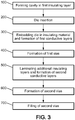
Figure 3 is a diagram showing the main steps of a manufacturing process according to an embodiment of the invention. -
Figures 4a to 4d schematically represent the main steps of a manufacturing process according to an embodiment of the invention. - With reference to
figures 1a and 1b , apre-packed power cell 1 according an embodiment of the invention will now be described. - The
pre-packed power cell 1 comprises apower die 10. The power die may be a diode or a transistor such as a MOSFET, JFET or IGBT. In embodiments, the power die 10 is made from a wide bandgap semiconductor, i.e a semiconductor having a bandgap in the range of 2-4 eV. For instance, the power die may be made in Silicon Carbide SiC or in Gallium Nitride GaN. - The power die has
electrical contacts 11 on opposite sides of the power die. In an embodiment, the power die 10 is a diode and has two electrical contacts. In another embodiment, the power die 10 is a transistor and has three electrical contacts comprising a gate, a source and a drain, or a gate, an emitter and a collector, according to the type of transistor. - The
pre-packed power cell 1 further comprises an electrically insulatingcore 20, in which the power die 10 is embedded. Preferably, the electrically insulating core has low thermal resistance to provide better heat dissipation. - The electrically insulating
core 20 may be made of FR-4 glass epoxy, polyimide, or in ceramic such as HTCC (High Temperature Co-fired Ceramic) or LTCC (Low Temperature Co-fired Ceramic). - In addition, the
pre-packed power cell 1 further comprises two first electricallyconductive layers 30, also embedded in the electrically insulatingcore 20 and arranged on both sides of the power die. Each first electricallyconductive layer 30 is connected to at least an electrical contact of the power die through respectivefirst vias 40 arranged in the electrically insulating substrate. - The first electrically
conductive layers 30 are patterned to be properly connected to the contacts of the power die. In particular, each electricallyconductive layer 30 has at least onecontact pad 31 adapted to be connected to a respective contact of the power die. - Last, the
pre-packed power cell 1 further comprises two second electricallyconductive layers 50, which are positioned on opposite main surfaces of the electrically insulatingcore 20. Each second electricallyconductive layer 50 is also patterned to provide appropriate connections to other components, for instance components of a power module. - Each second electrically
conductive layer 50 comprises at least onecontact pad 51 connected to arespective contact pad 31 of a first electricallyconductive layer 30 through respectivesecond vias 60 arranged in the electrically insulating substrate. - The first and second electrically conductive layers are preferably made in copper.
- In addition, as shown schematically on
figure 1 , the thickness of the second electricallyconductive layers 50 is greater than the thickness of the first electricallyconductive layers 30. Preferably, the thickness of the second electrically conductive layers is at least ten times the thickness of the first electrically conductive layers. For instance, the thickness of the first electrically conductive layers may be about 35 µm, and the thickness of the second electrically conductive layers may be at least 70 µm, for instance equal to 400 µm. - Moreover, the surface area of a contact pad of a second electrically
conductive layer 50 is greater than or equal to the surface area of thecontact pad 31 of a first electricallyconductive layer 31 to which it is connected; and the surface area of saidcontact pad 31 of the first electricallyconductive layer 30 is greater than the surface area of the power dieelectrical contact 11 to which it is connected. - The
contact pads 51 of a second electrically conductive layer also formelectrical contacts 2 of thepower cell 1, for its connection to other components, for instance within a power module. - Therefore, the electrical contacts of the
power cell 1 are larger than those 11 of the power die 10. This offers an improved and a flexible fan out for a final assembly process of a power module including such a power cell. It also reduces the complexity and the precision requested during the assembly process. - Moreover, the thick second
conductive layers 50 allow high current flow to the power die by decreasing the resistivity of the current path. This current flow is transmitted to the thin firstconductive layers 30 through thesecond vias 60, and in turn to the power die 10 through thefirst vias 40. To this end, given the reduced surface area of the power dieelectrical contacts 11, thefirst vias 40 are arranged with a density of at least 30 vias/mm2, for instance with a ratio vias hole depth to drill diameter of 1:2.5. - The connection surface between each first electrically conductive layer and a respective second electrically conductive layer being greater, the density of
second vias 60 needs not be as high. It is therefore inferior or equal to the density of thefirst vias 40. For instance, it can thus inferior or equal to 30 vias/mm2. In that case the diameter of thesecond vias 60 can be greater than the diameter of the first vias. For example, with a ratio vias hole depth to drill diameter of 1:1. - This connection to the power die allows a low impact on the resistivity of the assembly stack. In particular, the on and off resistance of the power die are not affected and the electric losses are quite low. This important density of vias also contributes to heat dissipation.
- In an embodiment, an example of which being shown on
figure 1a , the pre-packed power cell comprises only a power die. In this embodiment, integration of thepower cell 1 in a power module is rendered easy because the connection of power cell electrical contacts to a substrate is easier than with smaller contacts of a power die. Thus it is no longer necessary to adapt the design of a power module to the design or the connection possibilities of a cell; hence new design possibilities are offered. - In an alternative embodiment, the
power cell 1 may incorporate other components. In a preferred embodiment, thepower cell 1 comprises, in addition to apower die 10, a control die 70 adapted to control the power die 10. - In that case, the control die 70, also having respective
electrical contacts 71, is also embedded in the electrically insulating substrate. The control die 70 is connected to the power die through the first electrically conductive layers, to which it is connected bythird vias 80. The control die 70 is thus also connected to the second electricallyconductive layers 50 through the first electricallyconductive layers 30, and can be controlled by respectiveelectrical contacts 3 arranged in the second electrically conductive layers. - This embodiment is particularly preferred for power dies made of wide bandgap semiconductors, because the latter exhibit high commutation frequencies, and the incorporation of a power die in the power cell allows bringing the control die closer to the power die and hence reducing parasites in their connection.
- The
power cell 1 may further comprise additional components (not shown), for instance passive components such as capacitors, or integrated circuit dies, to incorporated additional functionalities. In that case, these components are also embedded in the electrically insulating substrates, and connected to the second electrically conductive layers by respective vias (not shown). - With reference to
figure 2 , apower module 9 is shown, comprising a plurality ofpre-packed power cells 1 according to the description above. The power module can be for instance an inverter or a power converter. - The
power module 9 may comprise at least onesubstrate 90 having alayer 91 of highly thermally conductive material on which an electrically conductive layer 92 (e.g. copper layer) is patterned to match the size and shape of the electrical contacts of thepre-packaged power cell 1 and to provide the desired connections between the dies contained in therespective power cells 1. Eachpower cell 1 is attached on one side of the substrate by an electrically and thermallyconductive interconnection material 93 such as solder, silver sinter or conductive paste. - With reference to
figure 3 , a method for manufacturing apre-packed power cell 1 according to the description above will now be described. - During a
first step 100, at least one cavity having the size of a power die is formed in afirst layer 20a of electrically insulating material. The cavity may be obtained by positioning a wedge having the size of a power die during the manufacturing of the first layer, and then removing the wedge. - During a
second step 200, apower die 10 is inserted in the cavity.Figure 4a represents the structure obtained at the end ofstep 200. - In an embodiment in which the pre-packed power cell comprises another cavity, for instance for a control die of the power die, step 100 also comprises forming an additional cavity for the control die. Step 200 then comprises the insertion of the control die in the additional cavity.
- During a
step 300, asecond layer 20b of electrically insulating material is laminated on top of thefirst layer 20a in order to embed the power die therein. This step also comprises forming, on opposite main surfaces of the thus obtained layer of electrically insulating material, two first electricallyconductive layers 30. In one embodiment, the two first electricallyconductive layers 30 may be obtained by electrodeposition. In another embodiment, step 300 may comprise laminating second layers 22 of electrically insulating material and first layers of electrically conductive material simultaneously on opposite sides of the layer of electrically insulating material embedding the power die. The first electrically conductive layers are etched to obtain the desired connection patterns. - At this point an
intermediate structure 5 comprising alayer 20c of electrically insulating material between two first layers of electrically conductive material is obtained. A schematic representation of thisintermediate structure 5 is shown infigure 4b . - As schematically shown in
figure 4c , during astep 400 first holes are drilled and metallized to form the plurality of first vias at the desired density of at least 30 vias/mm2, the vias extending from each first layer of electrically conductive material to the electrical contacts of the power die. The drilling step may be performed by laser drilling. - A
step 500 then comprises laminating additional electrically insulating layers on opposite main surfaces are formed on opposite main free surfaces of theintermediate structure 5, and forming second electrically conductive layers on the additional insulating layers. This step is performed in a similar way asstep 300, except it comprises additional steps of metal deposition in order to obtain the desired thickness of the second electrically conductive layers. The second electrically conductive layers are then etched to obtain the desired connection patterns. - During a
step 600, second holes are drilled and metallized in order to obtain second vias connecting the second electrically conductive layers to the first ones. This step can be performed by mechanical drilling. - As mentioned hereinbefore, the density of the second vias can be lower than the density of the first vias and hence the diameter of the second vias can be more important, for instance with a ratio hole depth to drill diameter of 1:1 . In that case, the method can then comprise an
additional step 700, of filling the second vias with electrically conductive material so that the second vias can transmit a desired current density to the first electrically conductive layers. This step can be performed by electrodeposition. - In an embodiment, the method comprises forming at
step 500 second electrically conductive layers at a thickness lower than the desired thickness, forming the second vias atstep 600, and then filling the vias and increasing the thickness of the second electrically conductive layers atstep 700 by electrodeposition. - The
pre-packed power cell 1 is then obtained and shown schematically infigure 4d . Additionally, some specific treatments, which may be chemical, mechanical or other, may be performed on the second electricallyconductive layers 50 in order to facilitate interfacing of the power cell to an external assembly. As a non-limiting example, those treatments can comprise deposition on the surface of the pre-packed power cell of other metals such as a Nickel-gold or Silver deposition for latter sintering. - If the pre-packed power cell comprises additional components such as passive components, they can be embedded in the electrically insulating core with the power dies and connected to the second layers of electrically conductive materials through vias arranged in the core.
in that the surface area of a contact pad of a first electrically conductive layer is greater than the surface area of the electrical contact of the power die to which it is connected,
and in that the surface area of a contact pad of a second electrically conductive layer is greater or equal to than the surface area of the contact pad of the first electrically conductive layer to which it is connected.
Claims (15)
- A pre-packed power cell (1) comprising :- a power die (10), having at least two electrical contacts (11) on opposite sides of the power die (10),- an electrically insulating core (20), wherein the power die (10) is embedded in the electrically insulating core (20),- two first electrically conductive layers (30) embedded in the electrically insulating core (20) and having contact pads (31) respectively connected to each electrical contact (11) of the power die (10) through first vias (40) arranged in the electrically insulating core (20),- two second electrically conductive layers (50) on opposite main surfaces of the core (20), and having contact pads (51) respectively connected to the contact pads (31) of each first electrically conductive layer (30) through second vias (60) arranged in the electrically insulating core (20),characterized in that the second electrically conductive layers (50) have a thickness greater than the thickness of the first electrically conductive layers (30),
in that the surface area of a contact pad (31) of a first electrically conductive layer (30) is greater than the surface area of the electrical contact (11) of the power die (10) to which it is connected,
and in that the surface area of a contact pad (51) of a second electrically conductive layer (50) is greater or equal to than the surface area of the contact pad (31) of the first electrically conductive layer (30) to which it is connected. - A pre-packed power cell according to claim 1, wherein the thickness of the second electrically conductive layers (50) is at least ten times the thickness of the first electrically conductive layers (30).
- A pre-packed power cell according to claim 1 or 2, wherein the electrically insulating core (20) is made in one of the following materials: FR4, polyimide, HTCC, LTCC.
- A pre-packed power cell (1) according to any of the preceding claims, wherein the pre-packed power cell (1) has electrical contacts (2) arranged in the second electrically conductive layers (50), and formed by the contact pads (51) of said second electrically conductive layers (50).
- A pre-packed power cell (1) according to any of the preceding claims, comprising a density of first vias (40) between each first electrically conductive layer (30) and respectively each electrical contact (11) of the power die (10) of at Ieast30 vias/mm2.
- A pre-packed power cell (1) according to any of the preceding claims, comprising a density of second vias (60) between each first electrically conductive layer (30) and respectively each second electrically conductive layer (50) lower or equivalent than the density of first vias. 2.
- A pre-packed power cell (1) according to any of the preceding claims, further comprising a control die (70) adapted to control the power die (10), the control die (70) being embedded in the electrically insulating core (20) and being connected to the first electrically conductive layers (30) by third vias (80) arranged in the electrically insulating core.
- A pre-packed power cell according to claim 8, wherein the power die (10) is connected to the control die (70) through the first electrically conductive layers (30).
- A pre-packed power cell (1) according to claim 8 or 9, wherein the power die (10) is a wide band gap semiconductor device.
- A pre-packed power cell (1) according to any of the preceding claims, further comprising at least one passive component embedded in the electrically insulating core and being connected to the second electrically conductive layers by fourth vias.
- A power module (9), comprising at least a substrate (90) and a plurality of power dies (10) connected to the substrate (90), wherein the power module (9) comprises at least one pre-packed power cell (1) according to any of the preceding claims, each pre-packed power cell (1) being connected to the substrate (90) and incorporating one of the power dies (10) of the power module.
- A method for manufacturing a pre-packed power cell (1) according to any of claims 1 to 10, comprising :- forming (100) at least a cavity of a size of a power die in a first layer (20a) of electrically insulating material,- placing (200) the or each power die in a respective cavity,- laminating (300) an electrically isolating layer (20b) and first electrically conductive layers (30) on opposite sides of the obtained layer of electrically isolating layer in order to obtain an intermediate structure (5) comprising a layer of electrically insulating material, embedding the power die, between two first layers of electrically conductive material,- drilling (400) first holes and metallizing the first holes in order to connect the at least one power die to the electrically conductive layers,- etching the first electrically conductive layers in order to obtain a layout,- laminating (500) additional isolation layers and on opposite main surfaces of the intermediate structure, and providing second electrically conductive layer on each additional isolation layer, wherein the second additional conductive layers have a thickness greater than the thickness of the first electrically conductive layers,- drilling (600) second holes and metallizing the second holes in order to connect the first and additional conductive layers,- etching the second electrically conductive layers in order to obtain another layout.
- A method according to claim 12, wherein the first drilling step (400) is performed by laser drilling and the second drilling step (600) is performed by mechanical drilling.
- A method according to claim 12 or 13, wherein each step of metallizing holes is performed by electro-deposition.
- A method according to any of claims 12 to 14, wherein the second holes have a diameter of at least 0.4 mm, and the method further comprises a step of filling the second holes.
Priority Applications (2)
| Application Number | Priority Date | Filing Date | Title |
|---|---|---|---|
| EP18305373.5A EP3547359A1 (en) | 2018-03-30 | 2018-03-30 | Improved pre-packed power cell |
| PCT/JP2018/046672 WO2019187400A1 (en) | 2018-03-30 | 2018-12-12 | Pre-packed power cell, power module and method for manufacturing pre-packed power cell |
Applications Claiming Priority (1)
| Application Number | Priority Date | Filing Date | Title |
|---|---|---|---|
| EP18305373.5A EP3547359A1 (en) | 2018-03-30 | 2018-03-30 | Improved pre-packed power cell |
Publications (1)
| Publication Number | Publication Date |
|---|---|
| EP3547359A1 true EP3547359A1 (en) | 2019-10-02 |
Family
ID=61972064
Family Applications (1)
| Application Number | Title | Priority Date | Filing Date |
|---|---|---|---|
| EP18305373.5A Pending EP3547359A1 (en) | 2018-03-30 | 2018-03-30 | Improved pre-packed power cell |
Country Status (2)
| Country | Link |
|---|---|
| EP (1) | EP3547359A1 (en) |
| WO (1) | WO2019187400A1 (en) |
Cited By (2)
| Publication number | Priority date | Publication date | Assignee | Title |
|---|---|---|---|---|
| CN113380741A (en) * | 2020-03-10 | 2021-09-10 | 英飞凌科技股份有限公司 | Semiconductor device including parallel conductive layers |
| WO2022028915A1 (en) * | 2020-08-03 | 2022-02-10 | Robert Bosch Gmbh | Electronic circuit module |
Families Citing this family (3)
| Publication number | Priority date | Publication date | Assignee | Title |
|---|---|---|---|---|
| EP3716326A1 (en) * | 2019-03-25 | 2020-09-30 | Mitsubishi Electric R&D Centre Europe B.V. | Electrically power assembly with thick electrically conductive layers |
| DE102021101010A1 (en) | 2021-01-19 | 2022-07-21 | Infineon Technologies Ag | PRE-PACKAGED CHIP, METHOD OF MAKING A PRE-PACKAGED CHIP, SEMICONDUCTOR PACKAGE AND METHOD OF MAKING A SEMICONDUCTOR PACKAGE |
| CN121335604B (en) * | 2025-12-10 | 2026-03-17 | 山东大学 | Embedded double-layer driving power module and preparation method thereof |
Citations (4)
| Publication number | Priority date | Publication date | Assignee | Title |
|---|---|---|---|---|
| DE102008040906A1 (en) * | 2008-07-31 | 2010-02-04 | Robert Bosch Gmbh | Printed circuit board with electronic component |
| US20160240471A1 (en) | 2014-04-16 | 2016-08-18 | Gan Systems Inc. | EMBEDDED PACKAGING FOR DEVICES AND SYSTEMS COMPRISING LATERAL GaN POWER TRANSISTORS |
| US9425131B2 (en) | 2014-03-05 | 2016-08-23 | Delta Electronics Int'l (Singapore) Pte Ltd | Package structure |
| US20160293579A1 (en) * | 2015-04-03 | 2016-10-06 | Globalfoundries Inc. | Integration structures for high current applications |
-
2018
- 2018-03-30 EP EP18305373.5A patent/EP3547359A1/en active Pending
- 2018-12-12 WO PCT/JP2018/046672 patent/WO2019187400A1/en not_active Ceased
Patent Citations (4)
| Publication number | Priority date | Publication date | Assignee | Title |
|---|---|---|---|---|
| DE102008040906A1 (en) * | 2008-07-31 | 2010-02-04 | Robert Bosch Gmbh | Printed circuit board with electronic component |
| US9425131B2 (en) | 2014-03-05 | 2016-08-23 | Delta Electronics Int'l (Singapore) Pte Ltd | Package structure |
| US20160240471A1 (en) | 2014-04-16 | 2016-08-18 | Gan Systems Inc. | EMBEDDED PACKAGING FOR DEVICES AND SYSTEMS COMPRISING LATERAL GaN POWER TRANSISTORS |
| US20160293579A1 (en) * | 2015-04-03 | 2016-10-06 | Globalfoundries Inc. | Integration structures for high current applications |
Cited By (11)
| Publication number | Priority date | Publication date | Assignee | Title |
|---|---|---|---|---|
| CN113380741A (en) * | 2020-03-10 | 2021-09-10 | 英飞凌科技股份有限公司 | Semiconductor device including parallel conductive layers |
| DE102020106518A1 (en) | 2020-03-10 | 2021-09-16 | Infineon Technologies Ag | Semiconductor devices having parallel electrically conductive layers |
| US20210287964A1 (en) * | 2020-03-10 | 2021-09-16 | Infineon Technologies Ag | Semiconductor devices including parallel electrically conductive layers |
| US12237246B2 (en) | 2020-03-10 | 2025-02-25 | Infineon Technologies Ag | Semiconductor devices including parallel electrically conductive layers |
| CN113380741B (en) * | 2020-03-10 | 2025-08-01 | 英飞凌科技股份有限公司 | Semiconductor device including parallel conductive layers |
| WO2022028915A1 (en) * | 2020-08-03 | 2022-02-10 | Robert Bosch Gmbh | Electronic circuit module |
| CN116097434A (en) * | 2020-08-03 | 2023-05-09 | 罗伯特·博世有限公司 | Electronic circuit module |
| JP2023536196A (en) * | 2020-08-03 | 2023-08-23 | ローベルト ボツシユ ゲゼルシヤフト ミツト ベシユレンクテル ハフツング | electronic circuit module |
| US20230268278A1 (en) * | 2020-08-03 | 2023-08-24 | Robert Bosch Gmbh | Electronic circuit module |
| JP7577189B2 (en) | 2020-08-03 | 2024-11-01 | ローベルト ボツシユ ゲゼルシヤフト ミツト ベシユレンクテル ハフツング | Electronic Circuit Module |
| US12557673B2 (en) * | 2020-08-03 | 2026-02-17 | Robert Bosch Gmbh | Electronic circuit module |
Also Published As
| Publication number | Publication date |
|---|---|
| WO2019187400A1 (en) | 2019-10-03 |
Similar Documents
| Publication | Publication Date | Title |
|---|---|---|
| US8890310B2 (en) | Power module package having excellent heat sink emission capability and method for manufacturing the same | |
| US7566955B2 (en) | High-frequency chip packages | |
| WO2019187400A1 (en) | Pre-packed power cell, power module and method for manufacturing pre-packed power cell | |
| EP3584833B1 (en) | Power module with improved alignment | |
| CN116711469A (en) | Component carrier with electronic components and thermally conductive blocks on both sides | |
| KR20220139385A (en) | Electronic module and method of manufacturing electronic module | |
| JP7233621B1 (en) | Power module device with improved thermal performance | |
| US11217571B2 (en) | Power module and method for manufacturing power module | |
| US20180040562A1 (en) | Elektronisches modul und verfahren zu seiner herstellung | |
| CN106876350B (en) | Power module and manufacturing method thereof | |
| Schulz-Harder | DBC substrates as a base for power MCM's | |
| EP4607583A1 (en) | Power chip embedded package substrate and packaging method | |
| US11791254B2 (en) | Electrically power assembly with thick electrically conductive layers | |
| CN118919514A (en) | Hybrid packaging power module with component cavity and manufacturing method | |
| KR20230136459A (en) | Power semiconductor module and method for manufacturing thereof | |
| Böttcher et al. | Concepts for realizing High-Voltage Power Modules by Embedding of SiC Semiconductors | |
| KR102900755B1 (en) | Power semiconductor module and manufacturing method of the same | |
| CN118234111A (en) | Integrated product of power circuit board packaging and radiator and preparation method thereof | |
| CN118538697A (en) | Power module and method for manufacturing the same |
Legal Events
| Date | Code | Title | Description |
|---|---|---|---|
| PUAI | Public reference made under article 153(3) epc to a published international application that has entered the european phase |
Free format text: ORIGINAL CODE: 0009012 |
|
| STAA | Information on the status of an ep patent application or granted ep patent |
Free format text: STATUS: THE APPLICATION HAS BEEN PUBLISHED |
|
| AK | Designated contracting states |
Kind code of ref document: A1 Designated state(s): AL AT BE BG CH CY CZ DE DK EE ES FI FR GB GR HR HU IE IS IT LI LT LU LV MC MK MT NL NO PL PT RO RS SE SI SK SM TR |
|
| AX | Request for extension of the european patent |
Extension state: BA ME |
|
| STAA | Information on the status of an ep patent application or granted ep patent |
Free format text: STATUS: REQUEST FOR EXAMINATION WAS MADE |
|
| 17P | Request for examination filed |
Effective date: 20200217 |
|
| RBV | Designated contracting states (corrected) |
Designated state(s): AL AT BE BG CH CY CZ DE DK EE ES FI FR GB GR HR HU IE IS IT LI LT LU LV MC MK MT NL NO PL PT RO RS SE SI SK SM TR |
|
| REG | Reference to a national code |
Ref country code: DE Ref legal event code: R079 Free format text: PREVIOUS MAIN CLASS: H01L0023480000 Ipc: H10W0070050000 |
|
| GRAP | Despatch of communication of intention to grant a patent |
Free format text: ORIGINAL CODE: EPIDOSNIGR1 |
|
| STAA | Information on the status of an ep patent application or granted ep patent |
Free format text: STATUS: GRANT OF PATENT IS INTENDED |
|
| RIC1 | Information provided on ipc code assigned before grant |
Ipc: H10W 70/05 20260101AFI20260303BHEP Ipc: H10W 70/09 20260101ALI20260303BHEP Ipc: H10W 70/60 20260101ALN20260303BHEP Ipc: H10W 90/10 20260101ALN20260303BHEP Ipc: H10W 70/68 20260101ALN20260303BHEP Ipc: H10W 72/90 20260101ALN20260303BHEP Ipc: H10W 72/00 20260101ALN20260303BHEP |
|
| RAP3 | Party data changed (applicant data changed or rights of an application transferred) |
Owner name: MITSUBISHI ELECTRIC CORPORATION Owner name: MITSUBISHI ELECTRIC R&D CENTRE EUROPE BV |
|
| RIC1 | Information provided on ipc code assigned before grant |
Ipc: H10W 70/05 20260101AFI20260311BHEP Ipc: H10W 70/09 20260101ALI20260311BHEP Ipc: H10W 70/60 20260101ALN20260311BHEP Ipc: H10W 90/10 20260101ALN20260311BHEP Ipc: H10W 72/90 20260101ALN20260311BHEP Ipc: H10W 72/00 20260101ALN20260311BHEP Ipc: H10W 70/68 20260101ALN20260311BHEP |
|
| RIN1 | Information on inventor provided before grant (corrected) |
Inventor name: PERRIN, REMI Inventor name: MORAND, JULIEN Inventor name: MRAD, ROBERTO Inventor name: EWANCHUK, JEFFREY Inventor name: MOLLOV, STEFAN |
|
| INTG | Intention to grant announced |
Effective date: 20260319 |