EP3547047A1 - Apparatus and method for thermal stabilization of pcb-mounted electronic components within an enclosed housing - Google Patents
Apparatus and method for thermal stabilization of pcb-mounted electronic components within an enclosed housing Download PDFInfo
- Publication number
- EP3547047A1 EP3547047A1 EP19165730.3A EP19165730A EP3547047A1 EP 3547047 A1 EP3547047 A1 EP 3547047A1 EP 19165730 A EP19165730 A EP 19165730A EP 3547047 A1 EP3547047 A1 EP 3547047A1
- Authority
- EP
- European Patent Office
- Prior art keywords
- matrix
- electronic component
- devices
- thermosensitive
- thermoelectric devices
- Prior art date
- Legal status (The legal status is an assumption and is not a legal conclusion. Google has not performed a legal analysis and makes no representation as to the accuracy of the status listed.)
- Granted
Links
Images



Classifications
-
- H—ELECTRICITY
- H10—SEMICONDUCTOR DEVICES; ELECTRIC SOLID-STATE DEVICES NOT OTHERWISE PROVIDED FOR
- H10W—GENERIC PACKAGES, INTERCONNECTIONS, CONNECTORS OR OTHER CONSTRUCTIONAL DETAILS OF DEVICES COVERED BY CLASS H10
- H10W40/00—Arrangements for thermal protection or thermal control
- H10W40/20—Arrangements for cooling
- H10W40/28—Arrangements for cooling comprising Peltier coolers
-
- F—MECHANICAL ENGINEERING; LIGHTING; HEATING; WEAPONS; BLASTING
- F25—REFRIGERATION OR COOLING; COMBINED HEATING AND REFRIGERATION SYSTEMS; HEAT PUMP SYSTEMS; MANUFACTURE OR STORAGE OF ICE; LIQUEFACTION SOLIDIFICATION OF GASES
- F25B—REFRIGERATION MACHINES, PLANTS OR SYSTEMS; COMBINED HEATING AND REFRIGERATION SYSTEMS; HEAT PUMP SYSTEMS
- F25B21/00—Machines, plants or systems, using electric or magnetic effects
- F25B21/02—Machines, plants or systems, using electric or magnetic effects using Peltier effect; using Nernst-Ettinghausen effect
- F25B21/04—Machines, plants or systems, using electric or magnetic effects using Peltier effect; using Nernst-Ettinghausen effect reversible
-
- G—PHYSICS
- G05—CONTROLLING; REGULATING
- G05D—SYSTEMS FOR CONTROLLING OR REGULATING NON-ELECTRIC VARIABLES
- G05D23/00—Control of temperature
- G05D23/19—Control of temperature characterised by the use of electric means
- G05D23/1927—Control of temperature characterised by the use of electric means using a plurality of sensors
- G05D23/193—Control of temperature characterised by the use of electric means using a plurality of sensors sensing the temperaure in different places in thermal relationship with one or more spaces
- G05D23/1931—Control of temperature characterised by the use of electric means using a plurality of sensors sensing the temperaure in different places in thermal relationship with one or more spaces to control the temperature of one space
-
- H—ELECTRICITY
- H10—SEMICONDUCTOR DEVICES; ELECTRIC SOLID-STATE DEVICES NOT OTHERWISE PROVIDED FOR
- H10W—GENERIC PACKAGES, INTERCONNECTIONS, CONNECTORS OR OTHER CONSTRUCTIONAL DETAILS OF DEVICES COVERED BY CLASS H10
- H10W40/00—Arrangements for thermal protection or thermal control
- H10W40/70—Fillings or auxiliary members in containers or in encapsulations for thermal protection or control
-
- H—ELECTRICITY
- H10—SEMICONDUCTOR DEVICES; ELECTRIC SOLID-STATE DEVICES NOT OTHERWISE PROVIDED FOR
- H10W—GENERIC PACKAGES, INTERCONNECTIONS, CONNECTORS OR OTHER CONSTRUCTIONAL DETAILS OF DEVICES COVERED BY CLASS H10
- H10W42/00—Arrangements for protection of devices
- H10W42/20—Arrangements for protection of devices protecting against electromagnetic or particle radiation, e.g. light, X-rays, gamma-rays or electrons
-
- H—ELECTRICITY
- H10—SEMICONDUCTOR DEVICES; ELECTRIC SOLID-STATE DEVICES NOT OTHERWISE PROVIDED FOR
- H10W—GENERIC PACKAGES, INTERCONNECTIONS, CONNECTORS OR OTHER CONSTRUCTIONAL DETAILS OF DEVICES COVERED BY CLASS H10
- H10W74/00—Encapsulations, e.g. protective coatings
- H10W74/10—Encapsulations, e.g. protective coatings characterised by their shape or disposition
- H10W74/111—Encapsulations, e.g. protective coatings characterised by their shape or disposition the semiconductor body being completely enclosed
- H10W74/114—Encapsulations, e.g. protective coatings characterised by their shape or disposition the semiconductor body being completely enclosed by a substrate and the encapsulations
-
- F—MECHANICAL ENGINEERING; LIGHTING; HEATING; WEAPONS; BLASTING
- F25—REFRIGERATION OR COOLING; COMBINED HEATING AND REFRIGERATION SYSTEMS; HEAT PUMP SYSTEMS; MANUFACTURE OR STORAGE OF ICE; LIQUEFACTION SOLIDIFICATION OF GASES
- F25B—REFRIGERATION MACHINES, PLANTS OR SYSTEMS; COMBINED HEATING AND REFRIGERATION SYSTEMS; HEAT PUMP SYSTEMS
- F25B2321/00—Details of machines, plants or systems, using electric or magnetic effects
- F25B2321/02—Details of machines, plants or systems, using electric or magnetic effects using Peltier effects; using Nernst-Ettinghausen effects
- F25B2321/021—Control thereof
-
- H—ELECTRICITY
- H10—SEMICONDUCTOR DEVICES; ELECTRIC SOLID-STATE DEVICES NOT OTHERWISE PROVIDED FOR
- H10W—GENERIC PACKAGES, INTERCONNECTIONS, CONNECTORS OR OTHER CONSTRUCTIONAL DETAILS OF DEVICES COVERED BY CLASS H10
- H10W70/00—Package substrates; Interposers; Redistribution layers [RDL]
- H10W70/60—Insulating or insulated package substrates; Interposers; Redistribution layers
- H10W70/62—Insulating or insulated package substrates; Interposers; Redistribution layers characterised by their interconnections
- H10W70/63—Vias, e.g. via plugs
- H10W70/635—Through-vias
Definitions
- This invention relates generally to stabilizing the temperature of electronic components. More particularly, this invention is directed towards using a control processor for stabilizing thermal gradients across an electronic component that is PCB-mounted within an enclosed housing.
- PCBs Printed Circuit Boards
- a considerable amount of heat may be generated by electronic components during their operation, including transistors, integrated circuits, power controls, switches, oscillators, microprocessors, and the like.
- the heat generated may cause component failure or malfunction if not properly controlled.
- Certain types of electronic components may be particularly susceptible to heat dissipation or other temperature effects. In some cases, the temperature must be stabilized for the components to remain within their operating range.
- VXOs voltage-controlled crystal oscillators
- OXOs oven-controlled crystal oscillators
- PWE Pseudo-Wire Emulation
- VoIP Voice over IP
- video conferencing video conferencing
- streaming services including Pseudo-Wire Emulation (“PWE”), Voice over IP (“VoIP”), video conferencing, and streaming services.
- heat sinks are typically mounted on the active surface of a semiconductor die to absorb heat from the die and dissipate the heat by convection into the cooler air, thereby maintaining the temperature across the PCB.
- Temperatur compensation circuits which generally stabilize the performance of a given electronic component or PCB across a wide range of temperatures.
- temperature compensation circuits may provide a relatively flat frequency output over a wide range or temperatures.
- the PCB and temperature compensation circuits may be enclosed within a thermally-insulated enclosure or housing to protect the PCB and electronic components therein from outside environment hazards, such as ambient heat, moisture, dust, debris, and so on.
- Thermally-insulated housings may also be used to prevent electromagnetic signals generated by the electronic components from causing Electromagnetic Interference ("EMI”) or Radio Frequency Interference (“RFI”) to other devices in their vicinity and vice-versa.
- EMI Electromagnetic Interference
- RFID Radio Frequency Interference
- the thermally-insulated housings may also include temperature sensors to monitor the temperature around electronic components within the housings.
- one or more heating elements may be used together with the sensors to maintain a given temperature gradient across a component. Based on the temperature measured by the sensors, the heating elements may generate more or less heat to achieve the desired temperature gradient.
- a single planar heating element has been used to thermally stabilize electronic components mounted on a PCB within a thermally-insulated housing.
- a single planar heating element may stabilize time-based thermal fluctuations for a given electronic component, it may not compensate for thermal gradients across the physical dimensions of the component. These thermal gradients are dependent on the relative positions of other heat-generating electronic components on the PCB, such as power supplies.
- a set of linear heating elements that are closely spaced and in parallel may also be used. Although a set of linear heating elements may provide some capability to vary the heating across the physical dimensions of the component, the set may be insufficient to eliminate output fluctuations that degrade real-time applications and services, such as in the case of VCXOs and OCXOs that must maintain a flat frequency output over a wide range of temperatures.
- An apparatus, controller and method are described to stabilize the temperature across an electronic component.
- One embodiment of the invention includes an apparatus having a matrix of thermoelectric devices to set thermal gradients across the electronic component, a matrix of thermosensitive devices to measure thermal gradients associated with the electronic component and a controller for controlling the matrix of thermoelectric devices based on the thermal gradients measured by the matrix of thermosensitive devices with a matrix of thermocouple coefficients.
- Another embodiment of the invention includes a controller with executable instructions to detect thermal gradients measured by a matrix of thermosensitive devices associated with an electronic component and to control a set of current values applied to a matrix of thermoelectric devices based on the detected thermal gradients and with a matrix of thermocouple coefficients.
- a further embodiment of the invention includes a method for stabilizing the temperature of an electronic component mounted in a printed circuit board substrate within an enclosed housing.
- the electronic component is heated with a matrix of thermoelectric devices arranged in a first surface of the substrate opposite to a second surface of the substrate mounting the electronic component.
- Thermal gradients surrounding the electronic component are measured with a matrix of thermosensitive devices mounted on the second surface of the substrate.
- the heat applied by the matrix of thermoelectric devices is controlled based on the thermal gradients measured by the matrix of thermosensitive devices.
- an electronic component may be any electronic element packaged in a discrete form with two or more connecting leads or pads.
- Electronic components may be packaged singly, such as resistors, capacitors, and transistors, or in groups, such as in amplifiers, oscillators, and integrated circuits, among others.
- the electronic components may be typically mounted on Printed Circuit Boards ("PCBs"), which are used to mechanically support or electrically connect electronic components using conductive pathways or traces etched onto a non-conductive substrate.
- PCBs Printed Circuit Boards
- the electronic components may be through-hole or surface mounted.
- a PCB may be placed inside an enclosed volume or housing.
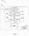
- FIG. 1 A schematic diagram of an apparatus for thermal stabilization of an electronic component constructed according to an embodiment of the invention is illustrated in FIG. 1 .
- Apparatus 100 is designed to stabilize the temperature around and across electronic component 105 mounted on multi-layer PCB substrate 110.
- Electronic component 105 is enclosed in thermally-stabilized housing 115, described in more detail herein below. It is appreciated that electronic component 105 may be through-hole or surface mounted on the surface of PCB substrate 110.
- Temperature stabilization is achieved with a matrix of thermoelectric devices including a plurality of thermoelectric devices 120a-m, a matrix of thermosensitive devices including a plurality of thermosensitive devices 125a-n, and a controller 130.
- a matrix of devices refers to a plurality of devices arranged in a two-dimensional pattern or grid.
- the matrix of devices may also include devices that are outside the two-dimensional grid, such as, for example, thermosensitive device 125n.
- thermoelectric devices 120a-m may be arranged in a two-dimensional grid on a surface of PCB substrate 110 opposite the electronic component 105, such as, for example, on the surface under the electronic component 105.
- the matrix of thermosensitive devices 125a-n may be arranged in a two-dimensional grid on a surface of PCB substrate 110 surrounding the perimeter of and on the same side as the electronic component 105. Some or all of thermosensitive devices 125a-n may also be in direct contact with electronic component 105, such as, for example, mounted on a surface of electronic component 105.
- one or more thermosensitive devices may be external to the thermally-stabilized housing 115 to measure thermal gradients associated with the PCB substrate 110 and the external ambient, such as thermosensitive device 125n.
- Controller 130 is used to control the plurality of thermoelectric devices 120a-m. Controller 130 generates a set of current values for the plurality of thermoelectric devices 120a-m. The plurality of thermoelectric devices 120a-m convert the set of current values into thermal gradients that are applied across the electronic component 105. It is appreciated that controller 130 may be within or external to the thermally-stabilized housing 115.
- the thermal gradients can be used to heat or cool the electronic component 105.
- the plurality of thermoelectric devices 120am may be a plurality of heating devices to heat the electronic component 105.
- a plurality of heating devices may be used to heat a crystal oscillator and maintain a constant temperature across the oscillator and within the thermally-stabilized housing 115.
- the plurality of thermoelectric devices 120a-m may be a plurality of cooling devices for cooling down electronic component 105 and preventing heat dissipation around the component 105.
- thermoelectric devices 120a-m may be hybrid heating and cooling devices, such as, for example, Peltier thermoelectric devices. It is appreciated that any combination of heating and cooling devices may be used in the matrix of thermoelectric devices 120a-m.
- the set of current values applied to the plurality of thermoelectric devices 120a-m are generated by the controller 130 based on thermal gradients measured by the plurality of thermosensitive devices 125a-n.
- the thermosensitive devices 125a-n may be arranged in a two-dimensional grid to detect the thermal gradients on the component side of the PCB substrate 110.
- the controller 130 receives the thermal gradients from the thermosensitive devices 125a-n and generates a set of current values for the thermoelectric devices 120a-m to convert into a set of thermal gradients applied across the electronic component 105.
- the set of current values are generated to maintain a desired temperature set-point across the electronic component 105 and within the thermally-stabilized housing 115.
- controller 130 is a Multiple-Input, Multiple-Output (“MIMO") controller.
- MIMO controller maintains a matrix of thermocouple coefficients ⁇ ij , which are measured in C°mm 2 /Watt.
- the matrix of thermocouple coefficients is a M x N matrix.
- thermoelectric devices 120a-m in relation to thermosensitive devices 125a-n yields a symmetric MIMO feedback matrix composed of the ⁇ ij coefficients. This reduces the complexity of the MIMO controller 130. Further, an equal number, N, of thermosensitive devices and thermoelectric devices ensures a square N x N feedback matrix and reduces the complexity of the MIMO controller 130.
- thermosensitive devices 125a-n may be a thermosensitive device external to the thermally-stabilized housing 115 to measure thermal gradients associated with the PCB substrate 110 and the external ambient, such as thermosensitive device 125n.
- the matrix of thermocouple coefficients may include parasitic impedance coefficients associated with the one or more external thermosensitive devices, such as external thermosensitive device 125n.
- thermocouple coefficients in the matrix are generated to maintain a desired temperature set-point across the electronic component 105 and within the thermally-stabilized housing 115.
- the desired temperature set-point may be initially set at an ambient temperature value of 65 °F.
- the thermocouple coefficients may be, in turn, initially set to achieve the initial temperature set-point across the electronic component 105. Accordingly, the thermocouple coefficients are in general kept constant to achieve the desired temperature set-point.
- the desired temperature set-point may be adjusted over time as the plurality of thermosensitive devices 125a-n detects different thermal gradients around the electronic component 105.
- the desired temperature set-point may be adjusted, for example, based on the average thermal gradients detected by the plurality of thermosensitive devices 125a-n measured over a 24-hour period.
- the thermocouple coefficients may be adjusted accordingly.
- the desired temperature set-point may be set at a value above the average thermal gradients detected in the past 24-hour period, such as, for example, at 25 °F degrees above the average. This provides a sufficient margin to ensure a stabilized temperature within the housing in cases where the temperature suddenly fluctuates between extremes in any given time period. This also ensures that the desired set-point will remain above the average thermal gradients at any given time.
- the desired temperature set-point may be adjusted differently, such as, for example, by setting it to be at or below the average thermal gradients detected in the past 24-hour period. Further, it is also appreciated that the desired temperature set-point may be maintained constant unless the temperature associated with the PCB substrate 110 and the ambient temperature exceed some pre-determined temperature bounds.
- each electronic component could have a set of thermoelectric devices and a set of thermosensitive devices associated with it.
- a single or multiple controllers could be used to control the temperature across the electronic components.
- Apparatus 100 includes dual-chambered enclosure 205 having upper metal housing 210 and lower metal housing 215 arranged so as to surround an internal area of multi-layer PCB substrate 220.
- Electronic component 225 to be thermally stabilized is mounted on multi-layer PCB substrate 220. Thermal conduction to the electronic component 225 is achieved by use of thermal conducting tape or foam 230 between the body of the electronic component 225 and the multi-layer PCB substrate 220.
- dual-chambered enclosure 205 may be a multi-chambered enclosure having more than two chambers.
- a multi-chambered housing may include housings within housings separated by insulative material.
- a matrix including a plurality of thermoelectric devices 235a-d is arranged in a two-dimensional grid on a surface of the multi-layer PCB substrate 220 opposite the electronic component 225.
- a matrix including a plurality of thermosensitive devices 240a-b is also arranged in a two-dimensional grid around the perimeter of the electronic component 225 for detecting the temperature across electronic component 225.
- the matrix also includes thermosensitive device 240c mounted on the top surface of electronic component 225.
- a controller (not shown in FIG. 2 ) controls the current values applied to the plurality of thermoelectric devices 235a-d based on thermal gradients detected by the plurality of thermosensitive devices 240a-c.
- Dual-chambered enclosure 205 also includes a conductive shield 245 surrounding the internal area of the multi-layer PCB substrate 220 in electrical contact with the upper and lower housings 210-215.
- an EMI/RFI shield 250 fully encloses the area around the electronic component 225.
- Upper and lower chambers 255a-b are formed by cavities cast into the upper and lower metal housings 210-215. For each housing, a tight EMI seal is formed into the surface of the PCB 220 and around the perimeter of the enclosed space by a metal-filled elastomer or polymer gasket material 260 that is contact to conductive shield 245 on both surfaces of PCB 220.
- the upper and lower housings 210-215 are kept in mechanical compression to ensure good conductivity and shielding around the entire perimeter of the electronic component 225. Plated through vias 265a-g are used to link the conductive shield 245 to conductive shield traces on the inner layers of PCB 220. The number and spacings of the vias and inner layer conductive shields are chosen to minimize EMI and RFI energy escaping or entering the upper and lower housings 210-215.
- An insulative material fills the upper and lower chambers 255a-b of upper and lower housings 210-215.
- the insulative material may be, for example, a high-density insulating Styrofoam.
- a plurality of openings 270a-b may also be disposed about in the PCB substrate 220 to interrupt any conductive transfer of heat that may take place during operation of the electronic component 225.
- electrical power, ground and other signals are provided to the enclosed area within the upper and lower housings 210-215 through regions intermediate the plurality of openings 270a-b.
- Power, ground and signal traces from the PCB 220 to the upper and lower chambers 255a-b may enter the chambers 255a-b through any number of isthmuses in PCB 220.
- the power, ground and signal traces may enter the chambers 255a-b through a single isthmus (such as shown in FIG. 3 ) to localize heat dissipation through the traces to one particular region.
- the power, ground and signal traces may be kept to a minimum to reduce the number of metal traces which are a major contributor to heat transfer between the upper and lower chambers 255a-b to the PCB 220.
- all of the internally controllable electronic components share a serial bus.
- the serial data signal may be used for the current values generated by the controller, such as controller 130 of FIG. 1 .
- capacitive or inductive coupling may be used on the signal paths to further reduce the number of traces.
- the signal paths may be encoded with an 8B/10B encoding to remove the DC component when using capacitive coupling.
- optical transmission may be used to limit the signal traces and thus reduce parasitic heat loss.
- FIG. 3 A top view of apparatus 100 is illustrated in FIG. 3 .
- Apparatus 100 is shown with a plurality of thermosensitive devices 240a-h arranged in a two-dimensional grid around the perimeter of electronic component 225 and on the same surface of PCB 220 as electronic component 225.
- Thermosensitive devices 240a-h are placed as close as possible to electronic component 225 to monitor the temperature of a region surrounding the component 225.
- thermosensitive devices 240a-i there are eight thermosensitive devices 240a-i. It is also appreciated that one or more of thermosensitive devices 240a-i may be in close thermal contact with electronic component 225. The one or more thermosensitive devices 240a-i may also be in direct contact with electronic component 225. For example, one or more thermosensitive devices may be mounted on the surface of electronic component 225, such as thermosensitive device 240c (shown in FIG. 2 ) mounted on top of electronic component 225.
- FIG. 3 also shows a set of void channels or perforations 270a-h in the PCB 220 arranged around the perimeter of electronic component 225 and internal to the EMI/RFI shield 250.
- Much of the heat leakage that occurs from within the EMI/RFI shield 250 to the external environment takes place through isthmuses 300a-h of PCB 220 intermediate the voids 270a-h.
- the placement of voids 270a-h reduces the heat conduction through the isthmuses 300a-h.
- Strategic placement of thermoelectric devices adjacent to the isthmuses 300a-h serves to combat the temperature gradients surrounding and across electronic component 225.
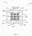
- thermoelectric devices 235a-i are also arranged in a two-dimensional grid but on a surface of PCB substrate 220 that surrounds and is opposite to the thermally stabilized region on the other side of PCB 220.
- the placement pattern for the thermoelectric devices 235a-i is intended for thermal dispersion in a given pattern, either uniform or not.
- thermoelectric devices 235a-i There are nine thermoelectric devices 235a-i as shown, with each one serving an area on the side opposite the electronic component 225.
- Metal-plate through vias may be dispersed on a metal surface to conduct heat from the surface mounting the thermoelectric devices 235a-i to the surface mounting the electronic component 225.
- Each thermoelectric device surface area may be separated from other thermoelectric devices to provide better separation of control in a given area.
- the thermally stabilized side surface area may be a single metal surface to disperse heat in a thermal dispersion pattern to the electronic component 225, either uniformly or not.
- thermoelectric device 500 is a heating device for heating an electronic component as described above.
- Serial Digital Analog Converter (“Serial DAC”) 505 receives serial data representing a set of current values from a controller, such as controller 130, at its "SDA” input.
- a serial clock signal is input into its "SCL” input and a supply voltage is input into the "V” input.
- Serial DAC 505 converts the serial data sent from the controller into a voltage output at "DOUT".
- the voltage output is passed to operational amplifier 510, which works as a low-pass filter to set the voltages across the heating device.
- the heating device is implemented with a power FET 515 in combination with a multiplicity of surface mounted resistors 520.
- the multiplicity of resistors 520 may be mounted on the PCB substrate in a dispersed pattern to provide a given distribution of heat to the electronic component in the area of the heating device.
- the resistors 520 may be uniformly distributed around power FET 515 to provide a uniform distribution of heat.
- the uniform distribution of heat enables a constant uniform temperature over the surface of the PCB substrate directly under the electronic component.
- the constant uniform temperature greatly improves the frequency stability of the oscillator in the thermally-stabilized housing.
- the resistors 520 may be spatially distributed around power FET 515 to provide a non-uniform distribution of heat.
- the non-uniform distribution of heat may be used, for example, to characterize the electronic component.
- the non-uniform distribution of heat may be used to determine the oscillator's frequency response over a wide range of temperatures. This may allow for any unknown oscillator to be used as the controller together with the thermoelectric devices and temperature sensors may set up thermal gradients around the oscillator to understand its response over a wide range of temperatures.
- the unknown oscillator may be, for example, an off-the-shelf, inexpensive component that has not yet been characterized.
Landscapes
- Engineering & Computer Science (AREA)
- Physics & Mathematics (AREA)
- Mechanical Engineering (AREA)
- Thermal Sciences (AREA)
- General Engineering & Computer Science (AREA)
- Remote Sensing (AREA)
- General Physics & Mathematics (AREA)
- Automation & Control Theory (AREA)
- Cooling Or The Like Of Electrical Apparatus (AREA)
- Cooling Or The Like Of Semiconductors Or Solid State Devices (AREA)
- Control Of Temperature (AREA)
Abstract
Description
- This application claims priority to
U.S. Provisional Application Ser. No. 60/839,515, filed August 22, 2006 - This invention relates generally to stabilizing the temperature of electronic components. More particularly, this invention is directed towards using a control processor for stabilizing thermal gradients across an electronic component that is PCB-mounted within an enclosed housing.
- Electronic components mounted on Printed Circuit Boards ("PCBs") are pervasive throughout a wide range of consumer and industrial products. With recent advances in semiconductor technologies, these electronic components have become smaller, faster, and more powerful. They have also become more densely packed in the PCBs, which may include many layers of intricate electrical circuits and connections supporting the components. This miniaturization has led to several new challenges in electronic component and PCB design, including the ability to control the heat generated by the electronic components during their operation.
- A considerable amount of heat may be generated by electronic components during their operation, including transistors, integrated circuits, power controls, switches, oscillators, microprocessors, and the like. The heat generated may cause component failure or malfunction if not properly controlled. Certain types of electronic components may be particularly susceptible to heat dissipation or other temperature effects. In some cases, the temperature must be stabilized for the components to remain within their operating range.
- For example, voltage-controlled crystal oscillators ("VCXOs") or oven-controlled crystal oscillators ("OCXOs"), are highly sensitive to temperature gradients, both in time and across their physical dimensions. These temperature gradients may result in undesirable output fluctuations such as thermally induced frequency drift. These output fluctuations may in turn impact the quality of real-time applications and services in computer networks where these oscillators are heavily used, including Pseudo-Wire Emulation ("PWE"), Voice over IP ("VoIP"), video conferencing, and streaming services.
- Conventional approaches to control or stabilize the temperature in a PCB include the use of heat sinks and temperature compensation circuits mounted on or external to the PCB, as well as thermally-insulated enclosures to house the PCB. For example, heat sinks are typically mounted on the active surface of a semiconductor die to absorb heat from the die and dissipate the heat by convection into the cooler air, thereby maintaining the temperature across the PCB.
- Additional temperature control may be provided by temperature compensation circuits which generally stabilize the performance of a given electronic component or PCB across a wide range of temperatures. In the case of VCXOs and OCXOs, temperature compensation circuits may provide a relatively flat frequency output over a wide range or temperatures.
- The PCB and temperature compensation circuits may be enclosed within a thermally-insulated enclosure or housing to protect the PCB and electronic components therein from outside environment hazards, such as ambient heat, moisture, dust, debris, and so on. Thermally-insulated housings may also be used to prevent electromagnetic signals generated by the electronic components from causing Electromagnetic Interference ("EMI") or Radio Frequency Interference ("RFI") to other devices in their vicinity and vice-versa.
- The thermally-insulated housings may also include temperature sensors to monitor the temperature around electronic components within the housings. In cases where temperature stability is desired for optimal performance, one or more heating elements may be used together with the sensors to maintain a given temperature gradient across a component. Based on the temperature measured by the sensors, the heating elements may generate more or less heat to achieve the desired temperature gradient.
- For example, a single planar heating element has been used to thermally stabilize electronic components mounted on a PCB within a thermally-insulated housing. Though a single planar heating element may stabilize time-based thermal fluctuations for a given electronic component, it may not compensate for thermal gradients across the physical dimensions of the component. These thermal gradients are dependent on the relative positions of other heat-generating electronic components on the PCB, such as power supplies.
- A set of linear heating elements that are closely spaced and in parallel may also be used. Although a set of linear heating elements may provide some capability to vary the heating across the physical dimensions of the component, the set may be insufficient to eliminate output fluctuations that degrade real-time applications and services, such as in the case of VCXOs and OCXOs that must maintain a flat frequency output over a wide range of temperatures.
- Accordingly, it would be desirable to provide a thermal-management approach that can effectively stabilize temperature gradients across an electronic component mounted on a PCB across both time and the physical dimensions of the component.
- An apparatus, controller and method are described to stabilize the temperature across an electronic component. One embodiment of the invention includes an apparatus having a matrix of thermoelectric devices to set thermal gradients across the electronic component, a matrix of thermosensitive devices to measure thermal gradients associated with the electronic component and a controller for controlling the matrix of thermoelectric devices based on the thermal gradients measured by the matrix of thermosensitive devices with a matrix of thermocouple coefficients.
- Another embodiment of the invention includes a controller with executable instructions to detect thermal gradients measured by a matrix of thermosensitive devices associated with an electronic component and to control a set of current values applied to a matrix of thermoelectric devices based on the detected thermal gradients and with a matrix of thermocouple coefficients.
- A further embodiment of the invention includes a method for stabilizing the temperature of an electronic component mounted in a printed circuit board substrate within an enclosed housing. The electronic component is heated with a matrix of thermoelectric devices arranged in a first surface of the substrate opposite to a second surface of the substrate mounting the electronic component. Thermal gradients surrounding the electronic component are measured with a matrix of thermosensitive devices mounted on the second surface of the substrate. The heat applied by the matrix of thermoelectric devices is controlled based on the thermal gradients measured by the matrix of thermosensitive devices.
- The invention is more fully appreciated in connection with the following detailed description taken in conjunction with the accompanying drawings, in which like reference characters refer to like parts throughout, and in which:
-
FIG. 1 illustrates a schematic diagram of an apparatus for thermal stabilization of an electronic component constructed according to an embodiment of the invention; -
FIG. 2 illustrates a side view of an apparatus for thermal stabilization of an electronic component constructed according to an embodiment of the invention; -
FIG. 3 illustrates a top view of an apparatus for thermal stabilization of an electronic component constructed according to an embodiment of the invention; -
FIG. 4 illustrates a bottom view of an apparatus for thermal stabilization of an electronic component constructed according to an embodiment of the invention; and -
FIG. 5 illustrates a circuit diagram for one exemplary embodiment of the thermoelectric devices shown inFIG. 4 . - An apparatus, controller, and method for stabilizing the temperature across an electronic component are provided. As generally used herein, an electronic component may be any electronic element packaged in a discrete form with two or more connecting leads or pads. Electronic components may be packaged singly, such as resistors, capacitors, and transistors, or in groups, such as in amplifiers, oscillators, and integrated circuits, among others. The electronic components may be typically mounted on Printed Circuit Boards ("PCBs"), which are used to mechanically support or electrically connect electronic components using conductive pathways or traces etched onto a non-conductive substrate. In accordance with the invention, the electronic components may be through-hole or surface mounted. Also in accordance with the invention, a PCB may be placed inside an enclosed volume or housing.
- A schematic diagram of an apparatus for thermal stabilization of an electronic component constructed according to an embodiment of the invention is illustrated in
FIG. 1 .Apparatus 100 is designed to stabilize the temperature around and across electronic component 105 mounted onmulti-layer PCB substrate 110. Electronic component 105 is enclosed in thermally-stabilizedhousing 115, described in more detail herein below. It is appreciated that electronic component 105 may be through-hole or surface mounted on the surface ofPCB substrate 110. - Temperature stabilization is achieved with a matrix of thermoelectric devices including a plurality of thermoelectric devices 120a-m, a matrix of thermosensitive devices including a plurality of
thermosensitive devices 125a-n, and acontroller 130. As generally used herein, a matrix of devices refers to a plurality of devices arranged in a two-dimensional pattern or grid. The matrix of devices may also include devices that are outside the two-dimensional grid, such as, for example,thermosensitive device 125n. - The matrix of thermoelectric devices 120a-m may be arranged in a two-dimensional grid on a surface of
PCB substrate 110 opposite the electronic component 105, such as, for example, on the surface under the electronic component 105. The matrix ofthermosensitive devices 125a-n may be arranged in a two-dimensional grid on a surface ofPCB substrate 110 surrounding the perimeter of and on the same side as the electronic component 105. Some or all ofthermosensitive devices 125a-n may also be in direct contact with electronic component 105, such as, for example, mounted on a surface of electronic component 105. In addition, one or more thermosensitive devices may be external to the thermally-stabilizedhousing 115 to measure thermal gradients associated with thePCB substrate 110 and the external ambient, such asthermosensitive device 125n. -
Controller 130 is used to control the plurality of thermoelectric devices 120a-m.Controller 130 generates a set of current values for the plurality of thermoelectric devices 120a-m. The plurality of thermoelectric devices 120a-m convert the set of current values into thermal gradients that are applied across the electronic component 105. It is appreciated thatcontroller 130 may be within or external to the thermally-stabilizedhousing 115. - The thermal gradients can be used to heat or cool the electronic component 105. In one exemplary embodiment, the plurality of thermoelectric devices 120am may be a plurality of heating devices to heat the electronic component 105. For example, a plurality of heating devices may be used to heat a crystal oscillator and maintain a constant temperature across the oscillator and within the thermally-stabilized
housing 115. In another exemplary embodiment, the plurality of thermoelectric devices 120a-m may be a plurality of cooling devices for cooling down electronic component 105 and preventing heat dissipation around the component 105. - In another exemplary embodiment, the plurality of thermoelectric devices 120a-m may be hybrid heating and cooling devices, such as, for example, Peltier thermoelectric devices. It is appreciated that any combination of heating and cooling devices may be used in the matrix of thermoelectric devices 120a-m.
- The set of current values applied to the plurality of thermoelectric devices 120a-m are generated by the
controller 130 based on thermal gradients measured by the plurality ofthermosensitive devices 125a-n. Thethermosensitive devices 125a-n may be arranged in a two-dimensional grid to detect the thermal gradients on the component side of thePCB substrate 110. Thecontroller 130 receives the thermal gradients from thethermosensitive devices 125a-n and generates a set of current values for the thermoelectric devices 120a-m to convert into a set of thermal gradients applied across the electronic component 105. The set of current values are generated to maintain a desired temperature set-point across the electronic component 105 and within the thermally-stabilizedhousing 115. - In one exemplary embodiment,
controller 130 is a Multiple-Input, Multiple-Output ("MIMO") controller. The MIMO controller maintains a matrix of thermocouple coefficients Θij, which are measured in C°mm2/Watt. Each thermocouple coefficient Θij is expressed as Θij = Tj/Vi, where Tj represents a thermal gradient detected by thermosensitive device j and Vi represents a voltage per area applied to thermoelectric device i. With M thermoelectric devices and N thermosensitive devices, the matrix of thermocouple coefficients is a M x N matrix. - In one exemplary embodiment, a symmetric placement of thermoelectric devices 120a-m in relation to
thermosensitive devices 125a-n yields a symmetric MIMO feedback matrix composed of the Θij coefficients. This reduces the complexity of theMIMO controller 130. Further, an equal number, N, of thermosensitive devices and thermoelectric devices ensures a square N x N feedback matrix and reduces the complexity of theMIMO controller 130. - It is appreciated that one or more of the
thermosensitive devices 125a-n may be a thermosensitive device external to the thermally-stabilizedhousing 115 to measure thermal gradients associated with thePCB substrate 110 and the external ambient, such asthermosensitive device 125n. Accordingly, the matrix of thermocouple coefficients may include parasitic impedance coefficients associated with the one or more external thermosensitive devices, such as externalthermosensitive device 125n. - The thermocouple coefficients in the matrix are generated to maintain a desired temperature set-point across the electronic component 105 and within the thermally-stabilized
housing 115. In one exemplary embodiment, the desired temperature set-point may be initially set at an ambient temperature value of 65 °F. The thermocouple coefficients may be, in turn, initially set to achieve the initial temperature set-point across the electronic component 105. Accordingly, the thermocouple coefficients are in general kept constant to achieve the desired temperature set-point. - The desired temperature set-point may be adjusted over time as the plurality of
thermosensitive devices 125a-n detects different thermal gradients around the electronic component 105. The desired temperature set-point may be adjusted, for example, based on the average thermal gradients detected by the plurality ofthermosensitive devices 125a-n measured over a 24-hour period. The thermocouple coefficients may be adjusted accordingly. - In one exemplary embodiment, the desired temperature set-point may be set at a value above the average thermal gradients detected in the past 24-hour period, such as, for example, at 25 °F degrees above the average. This provides a sufficient margin to ensure a stabilized temperature within the housing in cases where the temperature suddenly fluctuates between extremes in any given time period. This also ensures that the desired set-point will remain above the average thermal gradients at any given time.
- It is appreciated that the desired temperature set-point may be adjusted differently, such as, for example, by setting it to be at or below the average thermal gradients detected in the past 24-hour period. Further, it is also appreciated that the desired temperature set-point may be maintained constant unless the temperature associated with the
PCB substrate 110 and the ambient temperature exceed some pre-determined temperature bounds. - In addition, it is appreciated that the number of devices shown in
FIG. 1 is shown for illustration purposes only. For example, multiple electronic components could be mounted onPCB substrate 110. In this case, each electronic component could have a set of thermoelectric devices and a set of thermosensitive devices associated with it. A single or multiple controllers could be used to control the temperature across the electronic components. - A side view of an apparatus for thermal stabilization of an electronic component constructed according to an embodiment of the invention is illustrated in
FIG. 2 .Apparatus 100 includes dual-chamberedenclosure 205 havingupper metal housing 210 andlower metal housing 215 arranged so as to surround an internal area ofmulti-layer PCB substrate 220.Electronic component 225 to be thermally stabilized is mounted onmulti-layer PCB substrate 220. Thermal conduction to theelectronic component 225 is achieved by use of thermal conducting tape orfoam 230 between the body of theelectronic component 225 and themulti-layer PCB substrate 220. - It is appreciated that dual-chambered
enclosure 205 may be a multi-chambered enclosure having more than two chambers. For example, a multi-chambered housing may include housings within housings separated by insulative material. - In accordance with the invention, a matrix including a plurality of
thermoelectric devices 235a-d is arranged in a two-dimensional grid on a surface of themulti-layer PCB substrate 220 opposite theelectronic component 225. A matrix including a plurality ofthermosensitive devices 240a-b is also arranged in a two-dimensional grid around the perimeter of theelectronic component 225 for detecting the temperature acrosselectronic component 225. The matrix also includesthermosensitive device 240c mounted on the top surface ofelectronic component 225. A controller (not shown inFIG. 2 ) controls the current values applied to the plurality ofthermoelectric devices 235a-d based on thermal gradients detected by the plurality ofthermosensitive devices 240a-c. - Dual-chambered
enclosure 205 also includes aconductive shield 245 surrounding the internal area of themulti-layer PCB substrate 220 in electrical contact with the upper and lower housings 210-215. In addition, an EMI/RFI shield 250 fully encloses the area around theelectronic component 225. Upper andlower chambers 255a-b are formed by cavities cast into the upper and lower metal housings 210-215. For each housing, a tight EMI seal is formed into the surface of thePCB 220 and around the perimeter of the enclosed space by a metal-filled elastomer orpolymer gasket material 260 that is contact toconductive shield 245 on both surfaces ofPCB 220. - The upper and lower housings 210-215 are kept in mechanical compression to ensure good conductivity and shielding around the entire perimeter of the
electronic component 225. Plated through vias 265a-g are used to link theconductive shield 245 to conductive shield traces on the inner layers ofPCB 220. The number and spacings of the vias and inner layer conductive shields are chosen to minimize EMI and RFI energy escaping or entering the upper and lower housings 210-215. - An insulative material fills the upper and
lower chambers 255a-b of upper and lower housings 210-215. The insulative material may be, for example, a high-density insulating Styrofoam. A plurality ofopenings 270a-b may also be disposed about in thePCB substrate 220 to interrupt any conductive transfer of heat that may take place during operation of theelectronic component 225. - It is appreciated that electrical power, ground and other signals are provided to the enclosed area within the upper and lower housings 210-215 through regions intermediate the plurality of
openings 270a-b. Power, ground and signal traces from thePCB 220 to the upper andlower chambers 255a-b may enter thechambers 255a-b through any number of isthmuses inPCB 220. In one exemplary embodiment, the power, ground and signal traces may enter thechambers 255a-b through a single isthmus (such as shown inFIG. 3 ) to localize heat dissipation through the traces to one particular region. Further, the power, ground and signal traces may be kept to a minimum to reduce the number of metal traces which are a major contributor to heat transfer between the upper andlower chambers 255a-b to thePCB 220. - In one exemplary embodiment, all of the internally controllable electronic components share a serial bus. In one embodiment, in addition to the power and ground traces, there may be additional signal traces that traverse the chambers' boundaries, such as, for example, a clock signal, a serial data signal, and a serial clock for the serial bus. The serial data signal may be used for the current values generated by the controller, such as
controller 130 ofFIG. 1 . - It is appreciated that capacitive or inductive coupling may be used on the signal paths to further reduce the number of traces. For example, the signal paths may be encoded with an 8B/10B encoding to remove the DC component when using capacitive coupling. In addition, optical transmission may be used to limit the signal traces and thus reduce parasitic heat loss.
- A top view of
apparatus 100 is illustrated inFIG. 3 .Apparatus 100 is shown with a plurality ofthermosensitive devices 240a-h arranged in a two-dimensional grid around the perimeter ofelectronic component 225 and on the same surface ofPCB 220 aselectronic component 225.Thermosensitive devices 240a-h are placed as close as possible toelectronic component 225 to monitor the temperature of a region surrounding thecomponent 225. - It is appreciated that a multiplicity of thermosensitive devices may be used to measure thermal gradients around the
component 225. As shown inFIG. 3 , there are eightthermosensitive devices 240a-i. It is also appreciated that one or more ofthermosensitive devices 240a-i may be in close thermal contact withelectronic component 225. The one or morethermosensitive devices 240a-i may also be in direct contact withelectronic component 225. For example, one or more thermosensitive devices may be mounted on the surface ofelectronic component 225, such asthermosensitive device 240c (shown inFIG. 2 ) mounted on top ofelectronic component 225. -
FIG. 3 also shows a set of void channels orperforations 270a-h in thePCB 220 arranged around the perimeter ofelectronic component 225 and internal to the EMI/RFI shield 250. Much of the heat leakage that occurs from within the EMI/RFI shield 250 to the external environment takes place throughisthmuses 300a-h ofPCB 220 intermediate thevoids 270a-h. The placement ofvoids 270a-h reduces the heat conduction through theisthmuses 300a-h. Strategic placement of thermoelectric devices adjacent to theisthmuses 300a-h serves to combat the temperature gradients surrounding and acrosselectronic component 225. - A set of thermoelectric devices adjacent to
isthmuses 300a-h is illustrated inFIG. 4 .Thermoelectric devices 235a-i are also arranged in a two-dimensional grid but on a surface ofPCB substrate 220 that surrounds and is opposite to the thermally stabilized region on the other side ofPCB 220. The placement pattern for thethermoelectric devices 235a-i is intended for thermal dispersion in a given pattern, either uniform or not. There are ninethermoelectric devices 235a-i as shown, with each one serving an area on the side opposite theelectronic component 225. - Metal-plate through vias may be dispersed on a metal surface to conduct heat from the surface mounting the
thermoelectric devices 235a-i to the surface mounting theelectronic component 225. Each thermoelectric device surface area may be separated from other thermoelectric devices to provide better separation of control in a given area. In one exemplary embodiment, the thermally stabilized side surface area may be a single metal surface to disperse heat in a thermal dispersion pattern to theelectronic component 225, either uniformly or not. - A circuit diagram for a thermoelectric device constructed in accordance with one embodiment of the invention is illustrated in
FIG. 5 . Thermoelectric device 500 is a heating device for heating an electronic component as described above. Serial Digital Analog Converter ("Serial DAC") 505 receives serial data representing a set of current values from a controller, such ascontroller 130, at its "SDA" input. A serial clock signal is input into its "SCL" input and a supply voltage is input into the "V" input.Serial DAC 505 converts the serial data sent from the controller into a voltage output at "DOUT". - The voltage output is passed to
operational amplifier 510, which works as a low-pass filter to set the voltages across the heating device. In one embodiment, the heating device is implemented with apower FET 515 in combination with a multiplicity of surface mountedresistors 520. The multiplicity ofresistors 520 may be mounted on the PCB substrate in a dispersed pattern to provide a given distribution of heat to the electronic component in the area of the heating device. - In one exemplary embodiment, the
resistors 520 may be uniformly distributed aroundpower FET 515 to provide a uniform distribution of heat. The uniform distribution of heat enables a constant uniform temperature over the surface of the PCB substrate directly under the electronic component. In the case where the electronic component is an oscillator, for example, the constant uniform temperature greatly improves the frequency stability of the oscillator in the thermally-stabilized housing. - In another exemplary embodiment, the
resistors 520 may be spatially distributed aroundpower FET 515 to provide a non-uniform distribution of heat. The non-uniform distribution of heat may be used, for example, to characterize the electronic component. In the case where the electronic component is an oscillator, the non-uniform distribution of heat may be used to determine the oscillator's frequency response over a wide range of temperatures. This may allow for any unknown oscillator to be used as the controller together with the thermoelectric devices and temperature sensors may set up thermal gradients around the oscillator to understand its response over a wide range of temperatures. The unknown oscillator may be, for example, an off-the-shelf, inexpensive component that has not yet been characterized. - The foregoing description, for purposes of explanation, used specific nomenclature to provide a thorough understanding of the invention. However, it will be apparent to one skilled in the art that specific details are not required in order to practice the invention. Thus, the foregoing descriptions of specific embodiments of the invention are presented for purposes of illustration and description. They are not intended to be exhaustive or to limit the invention to the precise forms disclosed; obviously, many modifications and variations are possible in view of the above teachings. The embodiments were chosen and described in order to best explain the principles of the invention and its practical applications, they thereby enable others skilled in the art to best utilize the invention and various embodiments with various modifications as are suited to the particular use contemplated. It is intended that the following claims and their equivalents define the scope of the invention.
- 1. An apparatus comprising:
- a matrix of thermoelectric devices to set thermal gradients across an electronic component;
- a matrix of thermosensitive devices to measure thermal gradients associated with the electronic component; and
- a controller for controlling the matrix of thermoelectric devices based on the thermal gradients measured by the matrix of thermosensitive devices with a matrix of thermocouple coefficients.
- 2. The apparatus of
Clause 1, wherein the electronic component is selected from a surface mounted and a through-hole mounted component mounted on a first surface of a printed circuit board substrate. - 3. The apparatus of
Clause 2, wherein the printed circuit board substrate includes an enclosed housing. - 4. The apparatus of
Clause 2, wherein the matrix of thermoelectric devices includes a plurality of thermoelectric devices arranged in a two-dimensional grid in a second surface of the substrate opposite the first surface. - 5. The apparatus of Clause 4, wherein the matrix of thermosensitive devices includes a plurality of thermosensitive devices mounted in a two-dimensional grid on the first surface of the substrate surrounding the electronic component.
- 6. The apparatus of Clause 5, wherein the plurality of thermosensitive devices are mounted on a surface of the electronic component.
- 7. The apparatus of Clause 4, wherein the plurality of thermoelectric devices comprises a plurality of heating devices having a plurality of resistive elements.
- 8. The apparatus of Clause 4, wherein the plurality of thermoelectric devices comprises a plurality of Peltier devices.
- 9. The apparatus of Clause 4, further comprising a thermal conducting compound between the electronic component and the second surface of the substrate.
- 10. The apparatus of
Clause 1, further comprising an electronic magnetic interference and radio frequency interference shield enclosing the electronic component. - 11. The apparatus of Clause 8, wherein the plurality of thermoelectric devices are arranged to distribute heat to the electronic component in a thermal dispersion pattern.
- 12. The apparatus of Clause 5, wherein the matrix of thermosensitive devices further comprises a thermosensitive device to measure ambient temperature within the enclosed housing.
- 13. The apparatus of
Clause 1, wherein the electronic component comprises a crystal oscillator. - 14. The apparatus of
Clause 1, wherein the controller comprises a multiple-input, multiple-output controller. - 15. The apparatus of
Clause 1, wherein the matrix of thermocouple coefficients comprises a plurality of thermocouple coefficients corresponding to a set of thermal gradients detected by the matrix of thermosensitive devices and a set of voltage values generated by the matrix of thermoelectric devices. - 16. A controller, comprising executable instructions to:
- detect thermal gradients measured by a matrix of thermosensitive devices associated with an electronic component; and
- control a set of current values applied to a matrix of thermoelectric devices based on the detected thermal gradients and with a matrix of thermocouple coefficients.
- 17. The controller of Clause 16, wherein the electronic component is selected from a surface mounted and a through-hole mounted component mounted on a first surface of a printed circuit board substrate.
- 18. The controller of Clause 16, wherein the printed circuit board substrate includes an enclosed housing.
- 19. The controller of Clause 18, wherein the controller is external to the enclosed housing.
- 20. The controller of Clause 16, wherein the matrix of thermoelectric devices includes a plurality of thermoelectric devices arranged in a two-dimensional grid in a second surface of the substrate opposite the first surface.
- 21. The controller of Clause 16, wherein the matrix of thermosensitive devices includes a plurality of thermosensitive devices mounted in a two-dimensional grid on the first surface of the substrate surrounding the electronic component.
- 22. The controller of Clause 20, wherein the plurality of thermoelectric devices comprises a plurality of heating devices having a plurality of resistive elements.
- 23. The controller of Clause 20, wherein the plurality of thermoelectric devices comprises a plurality of Peltier devices.
- 24. The controller of Clause 21, wherein the matrix of thermosensitive devices comprises an ambient thermosensitive device to measure ambient temperature within the enclosed housing.
- 25. The controller of Clause 24, wherein the matrix of thermocouple coefficients comprises a plurality of thermocouple coefficients corresponding to a set of thermal gradients detected by the matrix of thermosensitive devices and a set of voltage values generated by the matrix of thermoelectric devices.
- 26. The controller of Clause 25, wherein the matrix of thermocouple coefficients comprises parasitic thermal impedance coefficients for the ambient temperature measured by the ambient thermosensitive device.
- 27. The controller of Clause 26, configured to initialize the matrix of thermocouple coefficients.
- 28. The controller of Clause 27, wherein the matrix of thermocouple coefficients is configured to achieve a temperature set-point.
- 29. The controller of Clause 28, wherein the thermocouple coefficients are adjusted based on the temperature set-point.
- 30. The controller of Clause 28, wherein the temperature set-point is adjusted based on average thermal gradients measured over a given time period.
- 31. A method for stabilizing the temperature of an electronic component mounted in a printed circuit board substrate with enclosed housing, comprising:
- heating the electronic component with a matrix of thermoelectric devices arranged in a first surface of the substrate opposite to a second surface of the substrate mounting the electronic component;
- measuring thermal gradients surrounding the electronic component with a matrix of thermosensitive devices mounted on the second surface of the substrate; and
- controlling the heat applied by the plurality of thermoelectric devices based on the thermal gradients measured by the plurality of thermosensitive devices and with a matrix of thermocouple coefficients.
- 32. The method of Clause 31, wherein heating the electronic component comprises applying a set of currents to the matrix of thermoelectric devices for distributing heat in a thermal dispersion pattern to the electronic component.
- 33. The method of Clause 32, wherein measuring thermal gradients comprises measuring a temperature variation at the matrix of thermosensitive devices and an ambient temperature variation within the enclosed housing generated by the set of currents.
- 34. The method of Clause 33, wherein controlling the heat comprises controlling the set of currents applied to the matrix of thermoelectric devices.
Claims (15)
- An apparatus, comprising:a matrix of thermoelectric devices to set thermal gradients across an electronic component within an enclosed housing, wherein the electronic component is selected from a surface mounted and a through-hole mounted component mounted on a first surface of a printed circuit board substrate and the matrix of thermoelectric devices includes a plurality of thermoelectric devices arranged in a two-dimensional grid in a second surface of the substrate opposite the first surface;a matrix of thermosensitive devices to measure thermal gradients associated with the electronic component, the matrix of thermosensitive devices including a plurality of thermosensitive devices mounted in a two-dimensional grid on the first surface of the substrate surrounding the electronic component and a thermosensitive device to measure ambient temperature within the enclosed housing;a first thermosensitive device external to the enclosed housing for measuring an ambient temperature variation outside the enclosed housing;a controller for controlling heat applied by the matrix of thermoelectric devices based on the thermal gradients measured by the matrix of thermosensitive devices and the first thermosensitive device, and based on a matrix of thermocouple coefficients including parasitic thermal impedance coefficients associated with the ambient temperature variation measured by the first thermosensitive device.
- The apparatus of claim 4, wherein the plurality of thermosensitive devices are mounted on a surface of the electronic component.
- The apparatus of claim 1, wherein the plurality of thermoelectric devices comprises a plurality of heating devices having a plurality of resistive elements.
- The apparatus of claim 1, wherein the plurality of thermoelectric devices comprises a plurality of Peltier devices.
- The apparatus of claim 1, further comprising a thermal conducting compound between the electronic component and the second surface of the substrate.
- The apparatus of claim 1, further comprising an electronic magnetic interference and radio frequency interference shield enclosing the electronic component.
- The apparatus of claim 6, wherein the plurality of thermoelectric devices are arranged to distribute heat to the electronic component in a thermal dispersion pattern.
- The apparatus of claim 1, wherein the electronic component comprises a crystal oscillator.
- The apparatus of claim 1, wherein the controller comprises a multiple-input, multiple-output controller.
- The apparatus of claim 1, wherein the matrix of thermocouple coefficients comprises a plurality of thermocouple coefficients corresponding to a set of thermal gradients detected by the matrix of thermosensitive devices and a set of voltage values generated by the matrix of thermoelectric devices.
- A controller, comprising executable instructions to perform as the controller of any preceding claim.
- A method for stabilizing the temperature of an electronic component mounted on a printed circuit board substrate and within an enclosed housing, comprising:heating the electronic component with a matrix of thermoelectric devices arranged in a first surface of the substrate opposite to a second surface of the substrate mounting the electronic component;measuring thermal gradients surrounding the electronic component with a matrix of thermosensitive devices mounted on the second surface of the substrate;measuring an ambient temperature variation outside the enclosed housing with a first thermosensitive device external to the enclosed housing; andcontrolling the heat applied by the matrix of thermoelectric devices based on the thermal gradients measured by the matrix of thermosensitive devices and the first thermosensitive device, and based on a matrix of thermocouple coefficients including parasitic thermal impedance coefficients associated with the ambient temperature variation measured by the first thermosensitive device.
- The method of claim 12, wherein heating the electronic component comprises applying a set of currents to the matrix of thermoelectric devices for distributing heat in a thermal dispersion pattern to the electronic component.
- The method of claim 13, wherein measuring thermal gradients comprises measuring a temperature variation at the matrix of thermosensitive devices and an ambient temperature variation within the enclosed housing generated by the set of currents.
- The method of claim 14, wherein controlling the heat comprises controlling the set of currents applied to the matrix of thermoelectric devices.
Applications Claiming Priority (3)
| Application Number | Priority Date | Filing Date | Title |
|---|---|---|---|
| US83951506P | 2006-08-22 | 2006-08-22 | |
| EP07841188.1A EP2102721B1 (en) | 2006-08-22 | 2007-08-22 | Apparatus and method for thermal stabilization of pcb-mounted electronic components within an enclosed housing |
| PCT/US2007/076488 WO2008024821A2 (en) | 2006-08-22 | 2007-08-22 | Apparatus and method for thermal stabilization of pcb-mounted electronic components within an enclosed housing |
Related Parent Applications (2)
| Application Number | Title | Priority Date | Filing Date |
|---|---|---|---|
| EP07841188.1A Division EP2102721B1 (en) | 2006-08-22 | 2007-08-22 | Apparatus and method for thermal stabilization of pcb-mounted electronic components within an enclosed housing |
| EP07841188.1A Division-Into EP2102721B1 (en) | 2006-08-22 | 2007-08-22 | Apparatus and method for thermal stabilization of pcb-mounted electronic components within an enclosed housing |
Publications (2)
| Publication Number | Publication Date |
|---|---|
| EP3547047A1 true EP3547047A1 (en) | 2019-10-02 |
| EP3547047B1 EP3547047B1 (en) | 2021-05-19 |
Family
ID=39107622
Family Applications (2)
| Application Number | Title | Priority Date | Filing Date |
|---|---|---|---|
| EP07841188.1A Active EP2102721B1 (en) | 2006-08-22 | 2007-08-22 | Apparatus and method for thermal stabilization of pcb-mounted electronic components within an enclosed housing |
| EP19165730.3A Active EP3547047B1 (en) | 2006-08-22 | 2007-08-22 | Apparatus and method for thermal stabilization of pcb-mounted electronic components within an enclosed housing |
Family Applications Before (1)
| Application Number | Title | Priority Date | Filing Date |
|---|---|---|---|
| EP07841188.1A Active EP2102721B1 (en) | 2006-08-22 | 2007-08-22 | Apparatus and method for thermal stabilization of pcb-mounted electronic components within an enclosed housing |
Country Status (6)
| Country | Link |
|---|---|
| US (2) | US7603205B2 (en) |
| EP (2) | EP2102721B1 (en) |
| JP (1) | JP2010502017A (en) |
| CN (1) | CN101517496B (en) |
| CA (2) | CA2877959C (en) |
| WO (1) | WO2008024821A2 (en) |
Families Citing this family (42)
| Publication number | Priority date | Publication date | Assignee | Title |
|---|---|---|---|---|
| CN104990301B (en) | 2007-05-25 | 2019-04-16 | 詹思姆公司 | Distribution formula thermoelectricity heating and cooling system and method |
| US8042995B2 (en) * | 2007-06-07 | 2011-10-25 | Hewlett-Packard Development Company, L.P. | Method for monitoring temperature of computer components to determine ambient chassis temperature |
| US7821346B2 (en) * | 2007-08-24 | 2010-10-26 | Cts Corporation | Ovenized oscillator |
| WO2010135363A2 (en) | 2009-05-18 | 2010-11-25 | Bsst Llc | Temperature control system with thermoelectric device |
| EP2433321B1 (en) | 2009-05-18 | 2014-10-22 | Bsst Llc | Battery thermal management system |
| US8260474B2 (en) * | 2009-09-25 | 2012-09-04 | Intel Corporation | Sensor-based thermal specification enabling a real-time metric for compliance |
| JP5192469B2 (en) * | 2009-09-30 | 2013-05-08 | 株式会社日立製作所 | Electronic equipment cooling structure |
| FI20096021A0 (en) | 2009-10-06 | 2009-10-06 | Wallac Oy | Optical measuring instrument |
| EP2507910A1 (en) * | 2009-11-30 | 2012-10-10 | Imec | Dual-sensor temperature stabilization for integrated electrical component |
| US8996192B2 (en) * | 2011-02-16 | 2015-03-31 | Signalogic, Inc. | Thermal management for integrated circuits |
| US9020655B2 (en) * | 2011-02-16 | 2015-04-28 | Signalogic, Inc. | Thermal management for integrated circuits |
| JP2013004174A (en) * | 2011-06-10 | 2013-01-07 | Toshiba Lighting & Technology Corp | Lamp device |
| FR2978870B1 (en) * | 2011-08-01 | 2016-11-18 | Commissariat Energie Atomique | HOT POINT LOCATION DEVICE WITH THERMAL FLUXMETERS |
| KR101928005B1 (en) * | 2011-12-01 | 2019-03-13 | 삼성전자주식회사 | Thermoelectric cooling packages and thermal management methods thereof |
| DE112014000419T5 (en) * | 2013-01-14 | 2015-10-15 | Gentherm Incorporated | Thermoelectric based thermal management of electrical devices |
| CN103389749B (en) * | 2013-07-01 | 2015-12-23 | 浙江大学 | A kind of temperature control system |
| US9625186B2 (en) | 2013-08-29 | 2017-04-18 | Taiwan Semiconductor Manufacturing Co., Ltd. | Cooling system for 3D IC |
| US10690816B2 (en) | 2013-12-31 | 2020-06-23 | Cognex Corporation | Systems and methods reduce temperature induced drift effects on a liquid lens |
| US9575221B2 (en) * | 2013-12-31 | 2017-02-21 | Cognex Corporation | Systems and methods reduce temperature induced drift effects on a liquid lens |
| CN108055815B (en) | 2014-03-21 | 2020-04-21 | 华为终端有限公司 | mobile terminal |
| US9705062B2 (en) * | 2014-08-26 | 2017-07-11 | GM Global Technology Operations LLC | Encapsulation of high temperature thermoelectric modules |
| WO2016057558A1 (en) * | 2014-10-08 | 2016-04-14 | Remy Technologies, Llc | Centrally located control electronics for electric machine |
| GB2531260B (en) * | 2014-10-13 | 2019-08-14 | Bae Systems Plc | Peltier effect heat transfer system |
| KR20170095952A (en) | 2014-12-19 | 2017-08-23 | 젠썸 인코포레이티드 | Thermal conditioning systems and methods for vehicle regions |
| US10033354B2 (en) | 2015-02-10 | 2018-07-24 | Honeywell International Inc. | Systems and methods for device temperature stabilization |
| CN106163225A (en) * | 2015-04-28 | 2016-11-23 | 中兴通讯股份有限公司 | Calorie control method and device |
| US10625566B2 (en) | 2015-10-14 | 2020-04-21 | Gentherm Incorporated | Systems and methods for controlling thermal conditioning of vehicle regions |
| US9826574B2 (en) * | 2015-10-28 | 2017-11-21 | Watlow Electric Manufacturing Company | Integrated heater and sensor system |
| US10845375B2 (en) | 2016-02-19 | 2020-11-24 | Agjunction Llc | Thermal stabilization of inertial measurement units |
| US10631373B2 (en) | 2016-05-12 | 2020-04-21 | Ford Global Technologies, Llc | Heated windshield indicator |
| CN106559070A (en) * | 2016-10-18 | 2017-04-05 | 北京无线电计量测试研究所 | A kind of constant-temperature crystal oscillator |
| US10372182B2 (en) | 2017-01-13 | 2019-08-06 | International Business Machines Corporation | Reducing thermal cycling fatigue |
| US10962422B2 (en) | 2018-09-05 | 2021-03-30 | Hamilton Sundstrand Corporation | Differential and high rate of change temperature sensing circuit |
| KR20260006072A (en) | 2018-11-30 | 2026-01-12 | 젠썸 인코포레이티드 | Thermoelectric conditioning system and methods |
| CN109489299B (en) * | 2019-01-08 | 2023-11-28 | 广东富信科技股份有限公司 | Semiconductor refrigeration low-temperature plate cold source and its control method |
| CN109994437B (en) * | 2019-03-29 | 2021-11-19 | 上海天马微电子有限公司 | Chip packaging structure and manufacturing method thereof |
| TWI698949B (en) * | 2019-08-07 | 2020-07-11 | 台灣愛司帝科技股份有限公司 | Film structure, chip carrier assembly and chip carrier device |
| CN111376463A (en) * | 2020-04-19 | 2020-07-07 | 任永红 | High temperature mould rapid cooling equipment |
| CN111883516A (en) * | 2020-07-24 | 2020-11-03 | 青岛歌尔智能传感器有限公司 | Packaging structure and packaging method of integrated module and electronic equipment |
| KR102880185B1 (en) | 2020-11-24 | 2025-11-03 | 삼성전자주식회사 | Semiconductor module |
| US12581857B2 (en) * | 2021-09-22 | 2026-03-17 | Intel Corporation | Integrated thermoelectric device to mitigate integrated circuit hot spots |
| WO2025169030A1 (en) * | 2024-02-05 | 2025-08-14 | Corintis Sa | Thermal device |
Citations (5)
| Publication number | Priority date | Publication date | Assignee | Title |
|---|---|---|---|---|
| US3634653A (en) * | 1970-06-01 | 1972-01-11 | Monsanto Co | Thermostat circuit for electronic compartments |
| US6209631B1 (en) * | 1999-07-23 | 2001-04-03 | Esco Electronics Corporation | Thermal management apparatus for a sealed enclosure |
| US20030121905A1 (en) * | 2000-04-14 | 2003-07-03 | Ikuo Nanno | Controller, temperature regulator and heat treatment apparatus |
| US20050189342A1 (en) * | 2004-02-23 | 2005-09-01 | Samer Kabbani | Miniature fluid-cooled heat sink with integral heater |
| US20060060964A1 (en) * | 2004-09-22 | 2006-03-23 | Christopher Golla | Method and apparatus for high temperature operation of electronics |
Family Cites Families (38)
| Publication number | Priority date | Publication date | Assignee | Title |
|---|---|---|---|---|
| US4317985A (en) | 1979-05-29 | 1982-03-02 | Hewlett-Packard Company | Dual heater stabilization apparatus and method for a crystal oven |
| JPS5824788A (en) * | 1981-08-07 | 1983-02-14 | 真空理工株式会社 | Temperature dradient furnace |
| US5180942A (en) | 1992-02-14 | 1993-01-19 | Motorola, Inc. | Thermally isolated ovenized crystal oscillator |
| US5456870A (en) | 1994-05-20 | 1995-10-10 | Van Dorn Demag Corporation | Barrel temperature state controller for injection molding machine |
| JPH09145644A (en) * | 1995-11-17 | 1997-06-06 | Shimadzu Corp | Analyzer with detection element that requires temperature control |
| US5659270A (en) | 1996-05-16 | 1997-08-19 | Motorola, Inc. | Apparatus and method for a temperature-controlled frequency source using a programmable IC |
| US5729181A (en) | 1996-08-23 | 1998-03-17 | Hewlett-Packard Company | High thermal gain oven with reduced probability of temperature gradient formation for the operation of a thermally stable oscillator |
| US5703542A (en) | 1996-08-28 | 1997-12-30 | Locus Incorporated | Compact temperature stabilized crystal oscillator |
| US5777524A (en) | 1997-07-29 | 1998-07-07 | Motorola, Inc. | Temperature compensation circuit for a crystal oscillator and associated circuitry |
| RU2122278C1 (en) | 1997-07-09 | 1998-11-20 | Открытое акционерное общество "МОРИОН" | Constant-temperature crystal oscillator and its temperature controller adjustment technique |
| US6362700B1 (en) | 1997-10-31 | 2002-03-26 | Cts Corporation | Temperature controlled compensated oscillator |
| US5917272A (en) | 1998-06-11 | 1999-06-29 | Vectron, Inc. | Oven-heated crystal resonator and oscillator assembly |
| US6166608A (en) | 1998-10-21 | 2000-12-26 | Symmetricom, Inc. | Thermo-electric cooled oven controlled crystal oscillator |
| JP2000183649A (en) * | 1998-12-18 | 2000-06-30 | Toyo Commun Equip Co Ltd | Highly stable piezoelectric oscillator |
| US6127661A (en) | 1999-04-07 | 2000-10-03 | Cts Corporation | Dynamic thermal control for ovenized oscillators |
| JP3601404B2 (en) * | 2000-03-09 | 2004-12-15 | 日本電気株式会社 | Peltier control device and Peltier element control method |
| JP4192393B2 (en) * | 2000-04-14 | 2008-12-10 | オムロン株式会社 | air conditioner |
| US6647428B1 (en) | 2000-05-05 | 2003-11-11 | Luminous Networks, Inc. | Architecture for transport of multiple services in connectionless packet-based communication networks |
| US7251256B1 (en) | 2000-05-18 | 2007-07-31 | Luminous Networks, Inc. | Synchronization of asynchronous networks using media access control (MAC) layer synchronization symbols |
| US6573704B2 (en) | 2000-12-21 | 2003-06-03 | Sun Microsystems, Inc. | Method and apparatus for isolating an ambient air temperature sensor |
| US6630872B1 (en) | 2001-07-20 | 2003-10-07 | Cmc Electronics, Inc. | Digital indirectly compensated crystal oscillator |
| JP3820942B2 (en) * | 2001-08-30 | 2006-09-13 | ヤマハ株式会社 | Thermoelectric module mounting apparatus and temperature control method thereof |
| GB0121375D0 (en) * | 2001-09-04 | 2001-10-24 | Ashe Morris Ltd | Temperature control systems |
| JP2003124662A (en) * | 2001-10-11 | 2003-04-25 | Mitsubishi Electric Corp | Automotive electronics |
| TWI251578B (en) * | 2001-12-11 | 2006-03-21 | Hitachi Building Sys Co Ltd | Magnetic brake system and elevator trouble detection system |
| JP4085236B2 (en) * | 2001-12-12 | 2008-05-14 | 株式会社安川電機 | Power module with cooling mechanism and cooling method thereof |
| US6501340B1 (en) | 2002-02-11 | 2002-12-31 | Acr Electronics, Inc. | Oscillator with frequency stabilizing circuit and method of constructing same |
| US6822515B2 (en) * | 2002-07-19 | 2004-11-23 | Ikuroh Ichitsubo | Accurate power sensing circuit for power amplifiers |
| JP2004071764A (en) * | 2002-08-05 | 2004-03-04 | Mitsubishi Heavy Ind Ltd | Electronic device cooler |
| DE10246910B4 (en) * | 2002-10-08 | 2004-11-04 | Mtu Aero Engines Gmbh | Multi-size control system and method for controlling a multi-size control system |
| JP2005183585A (en) * | 2003-12-18 | 2005-07-07 | Hitachi Ltd | Electronic equipment |
| WO2005101931A1 (en) * | 2004-04-15 | 2005-10-27 | Mitsubishi Denki Kabushiki Kaisha | Surface mounted component mounting structure |
| US7020540B2 (en) | 2004-05-14 | 2006-03-28 | D-M-E Company | Temperature control |
| JP4354347B2 (en) | 2004-06-29 | 2009-10-28 | 日本電波工業株式会社 | Crystal oscillator |
| US7253694B2 (en) | 2004-07-15 | 2007-08-07 | C-Mac Quartz Crystals, Limited | Temperature compensated oven controlled crystal oscillator |
| JP2006093893A (en) | 2004-09-21 | 2006-04-06 | Nippon Dempa Kogyo Co Ltd | Quartz crystal oscillator and heat insulation method in crystal oscillator |
| FR2879819B1 (en) * | 2004-12-21 | 2007-02-23 | Ulis Soc Par Actions Simplifie | COMPONENT FOR DETECTING ELECTROMAGNETIC RADIATION, IN PARTICULAR INFRARED |
| US20070251939A1 (en) * | 2006-04-27 | 2007-11-01 | Applied Materials, Inc. | Control scheme for cold wafer compensation on a lithography track |
-
2007
- 2007-08-22 CA CA2877959A patent/CA2877959C/en not_active Expired - Fee Related
- 2007-08-22 CN CN2007800359328A patent/CN101517496B/en active Active
- 2007-08-22 CA CA2661385A patent/CA2661385C/en not_active Expired - Fee Related
- 2007-08-22 EP EP07841188.1A patent/EP2102721B1/en active Active
- 2007-08-22 EP EP19165730.3A patent/EP3547047B1/en active Active
- 2007-08-22 WO PCT/US2007/076488 patent/WO2008024821A2/en not_active Ceased
- 2007-08-22 US US11/843,521 patent/US7603205B2/en active Active
- 2007-08-22 JP JP2009525752A patent/JP2010502017A/en active Pending
-
2009
- 2009-08-24 US US12/546,484 patent/US7698023B2/en active Active
Patent Citations (5)
| Publication number | Priority date | Publication date | Assignee | Title |
|---|---|---|---|---|
| US3634653A (en) * | 1970-06-01 | 1972-01-11 | Monsanto Co | Thermostat circuit for electronic compartments |
| US6209631B1 (en) * | 1999-07-23 | 2001-04-03 | Esco Electronics Corporation | Thermal management apparatus for a sealed enclosure |
| US20030121905A1 (en) * | 2000-04-14 | 2003-07-03 | Ikuo Nanno | Controller, temperature regulator and heat treatment apparatus |
| US20050189342A1 (en) * | 2004-02-23 | 2005-09-01 | Samer Kabbani | Miniature fluid-cooled heat sink with integral heater |
| US20060060964A1 (en) * | 2004-09-22 | 2006-03-23 | Christopher Golla | Method and apparatus for high temperature operation of electronics |
Also Published As
| Publication number | Publication date |
|---|---|
| US7603205B2 (en) | 2009-10-13 |
| CA2661385A1 (en) | 2008-02-28 |
| EP2102721A2 (en) | 2009-09-23 |
| EP3547047B1 (en) | 2021-05-19 |
| US20090312887A1 (en) | 2009-12-17 |
| EP2102721A4 (en) | 2017-07-05 |
| CA2661385C (en) | 2015-04-07 |
| JP2010502017A (en) | 2010-01-21 |
| CA2877959C (en) | 2017-06-13 |
| CA2877959A1 (en) | 2008-02-28 |
| US7698023B2 (en) | 2010-04-13 |
| US20080137309A1 (en) | 2008-06-12 |
| CN101517496B (en) | 2013-06-05 |
| EP2102721B1 (en) | 2019-05-08 |
| WO2008024821A2 (en) | 2008-02-28 |
| CN101517496A (en) | 2009-08-26 |
| WO2008024821A3 (en) | 2008-09-18 |
Similar Documents
| Publication | Publication Date | Title |
|---|---|---|
| EP2102721B1 (en) | Apparatus and method for thermal stabilization of pcb-mounted electronic components within an enclosed housing | |
| US6304450B1 (en) | Inter-circuit encapsulated packaging | |
| US7782147B2 (en) | Apparatus for providing oscillator frequency stability | |
| US20090051447A1 (en) | Ovenized oscillator | |
| EP2752103B1 (en) | Electronic device enclosures and heatsink structures with thermal management features | |
| US5180942A (en) | Thermally isolated ovenized crystal oscillator | |
| WO2009029209A1 (en) | Ovenized oscillator | |
| US20080030961A1 (en) | Multi-layered printed circuit board | |
| US6606246B2 (en) | Method and apparatus for retaining cooling apparatus and bus bar | |
| US20160322781A1 (en) | Dissipating heat from electronic devices | |
| US4841170A (en) | Temperature controlled hybrid assembly | |
| US12193143B2 (en) | Circuit board module | |
| US6423940B1 (en) | Temperature stabilization scheme for a circuit board | |
| US20130321088A1 (en) | Surface mount ovenized oscillator assembly | |
| EP2861048A1 (en) | Housing element for an electronic device | |
| USRE34179E (en) | Temperature controlled hybrid assembly | |
| US20250393114A1 (en) | Thermal control apparatus for an electronic component | |
| CN102469741B (en) | Circuit board radiating device and circuit board radiating method | |
| US12176255B2 (en) | Cantilevered dies in ceramic packages | |
| KR20160088239A (en) | Device for dissipating heat from at least one electronic component | |
| WO2023131847A1 (en) | Temperature stabilized frequency control device | |
| JP2000091714A (en) | Temperature adjusting structure for printed board | |
| JP2011100916A (en) | Mounting structure for heat dissipation of electronic component | |
| WO2019197804A1 (en) | Power supply apparatus | |
| JPH043997A (en) | Circuit board and manufacture thereof |
Legal Events
| Date | Code | Title | Description |
|---|---|---|---|
| PUAI | Public reference made under article 153(3) epc to a published international application that has entered the european phase |
Free format text: ORIGINAL CODE: 0009012 |
|
| STAA | Information on the status of an ep patent application or granted ep patent |
Free format text: STATUS: THE APPLICATION HAS BEEN PUBLISHED |
|
| AC | Divisional application: reference to earlier application |
Ref document number: 2102721 Country of ref document: EP Kind code of ref document: P |
|
| AK | Designated contracting states |
Kind code of ref document: A1 Designated state(s): AT BE BG CH CY CZ DE DK EE ES FI FR GB GR HU IE IS IT LI LT LU LV MC MT NL PL PT RO SE SI SK TR |
|
| STAA | Information on the status of an ep patent application or granted ep patent |
Free format text: STATUS: REQUEST FOR EXAMINATION WAS MADE |
|
| 17P | Request for examination filed |
Effective date: 20200320 |
|
| RBV | Designated contracting states (corrected) |
Designated state(s): AT BE BG CH CY CZ DE DK EE ES FI FR GB GR HU IE IS IT LI LT LU LV MC MT NL PL PT RO SE SI SK TR |
|
| RIC1 | Information provided on ipc code assigned before grant |
Ipc: H01L 23/42 20060101ALI20200730BHEP Ipc: H01L 23/552 20060101ALI20200730BHEP Ipc: H05B 3/02 20060101ALI20200730BHEP Ipc: F25B 21/02 20060101ALI20200730BHEP Ipc: F25B 21/04 20060101ALI20200730BHEP Ipc: G06F 15/00 20060101ALI20200730BHEP Ipc: H01L 23/38 20060101ALI20200730BHEP Ipc: G05D 23/00 20060101ALI20200730BHEP Ipc: H01L 23/498 20060101ALI20200730BHEP Ipc: H01L 23/31 20060101ALI20200730BHEP Ipc: G05D 23/19 20060101ALI20200730BHEP Ipc: G05B 13/02 20060101AFI20200730BHEP Ipc: H05B 1/02 20060101ALI20200730BHEP |
|
| GRAP | Despatch of communication of intention to grant a patent |
Free format text: ORIGINAL CODE: EPIDOSNIGR1 |
|
| STAA | Information on the status of an ep patent application or granted ep patent |
Free format text: STATUS: GRANT OF PATENT IS INTENDED |
|
| INTG | Intention to grant announced |
Effective date: 20201207 |
|
| GRAS | Grant fee paid |
Free format text: ORIGINAL CODE: EPIDOSNIGR3 |
|
| GRAA | (expected) grant |
Free format text: ORIGINAL CODE: 0009210 |
|
| STAA | Information on the status of an ep patent application or granted ep patent |
Free format text: STATUS: THE PATENT HAS BEEN GRANTED |
|
| AC | Divisional application: reference to earlier application |
Ref document number: 2102721 Country of ref document: EP Kind code of ref document: P |
|
| AK | Designated contracting states |
Kind code of ref document: B1 Designated state(s): AT BE BG CH CY CZ DE DK EE ES FI FR GB GR HU IE IS IT LI LT LU LV MC MT NL PL PT RO SE SI SK TR |
|
| REG | Reference to a national code |
Ref country code: GB Ref legal event code: FG4D |
|
| REG | Reference to a national code |
Ref country code: CH Ref legal event code: EP |
|
| REG | Reference to a national code |
Ref country code: DE Ref legal event code: R096 Ref document number: 602007061141 Country of ref document: DE |
|
| REG | Reference to a national code |
Ref country code: AT Ref legal event code: REF Ref document number: 1394593 Country of ref document: AT Kind code of ref document: T Effective date: 20210615 |
|
| REG | Reference to a national code |
Ref country code: IE Ref legal event code: FG4D |
|
| REG | Reference to a national code |
Ref country code: LT Ref legal event code: MG9D |
|
| REG | Reference to a national code |
Ref country code: AT Ref legal event code: MK05 Ref document number: 1394593 Country of ref document: AT Kind code of ref document: T Effective date: 20210519 |
|
| REG | Reference to a national code |
Ref country code: NL Ref legal event code: MP Effective date: 20210519 |
|
| PG25 | Lapsed in a contracting state [announced via postgrant information from national office to epo] |
Ref country code: AT Free format text: LAPSE BECAUSE OF FAILURE TO SUBMIT A TRANSLATION OF THE DESCRIPTION OR TO PAY THE FEE WITHIN THE PRESCRIBED TIME-LIMIT Effective date: 20210519 Ref country code: BG Free format text: LAPSE BECAUSE OF FAILURE TO SUBMIT A TRANSLATION OF THE DESCRIPTION OR TO PAY THE FEE WITHIN THE PRESCRIBED TIME-LIMIT Effective date: 20210819 Ref country code: LT Free format text: LAPSE BECAUSE OF FAILURE TO SUBMIT A TRANSLATION OF THE DESCRIPTION OR TO PAY THE FEE WITHIN THE PRESCRIBED TIME-LIMIT Effective date: 20210519 Ref country code: FI Free format text: LAPSE BECAUSE OF FAILURE TO SUBMIT A TRANSLATION OF THE DESCRIPTION OR TO PAY THE FEE WITHIN THE PRESCRIBED TIME-LIMIT Effective date: 20210519 |
|
| PG25 | Lapsed in a contracting state [announced via postgrant information from national office to epo] |
Ref country code: SE Free format text: LAPSE BECAUSE OF FAILURE TO SUBMIT A TRANSLATION OF THE DESCRIPTION OR TO PAY THE FEE WITHIN THE PRESCRIBED TIME-LIMIT Effective date: 20210519 Ref country code: PT Free format text: LAPSE BECAUSE OF FAILURE TO SUBMIT A TRANSLATION OF THE DESCRIPTION OR TO PAY THE FEE WITHIN THE PRESCRIBED TIME-LIMIT Effective date: 20210920 Ref country code: PL Free format text: LAPSE BECAUSE OF FAILURE TO SUBMIT A TRANSLATION OF THE DESCRIPTION OR TO PAY THE FEE WITHIN THE PRESCRIBED TIME-LIMIT Effective date: 20210519 Ref country code: LV Free format text: LAPSE BECAUSE OF FAILURE TO SUBMIT A TRANSLATION OF THE DESCRIPTION OR TO PAY THE FEE WITHIN THE PRESCRIBED TIME-LIMIT Effective date: 20210519 Ref country code: GR Free format text: LAPSE BECAUSE OF FAILURE TO SUBMIT A TRANSLATION OF THE DESCRIPTION OR TO PAY THE FEE WITHIN THE PRESCRIBED TIME-LIMIT Effective date: 20210820 Ref country code: IS Free format text: LAPSE BECAUSE OF FAILURE TO SUBMIT A TRANSLATION OF THE DESCRIPTION OR TO PAY THE FEE WITHIN THE PRESCRIBED TIME-LIMIT Effective date: 20210919 |
|
| PG25 | Lapsed in a contracting state [announced via postgrant information from national office to epo] |
Ref country code: NL Free format text: LAPSE BECAUSE OF FAILURE TO SUBMIT A TRANSLATION OF THE DESCRIPTION OR TO PAY THE FEE WITHIN THE PRESCRIBED TIME-LIMIT Effective date: 20210519 |
|
| PG25 | Lapsed in a contracting state [announced via postgrant information from national office to epo] |
Ref country code: RO Free format text: LAPSE BECAUSE OF FAILURE TO SUBMIT A TRANSLATION OF THE DESCRIPTION OR TO PAY THE FEE WITHIN THE PRESCRIBED TIME-LIMIT Effective date: 20210519 Ref country code: DK Free format text: LAPSE BECAUSE OF FAILURE TO SUBMIT A TRANSLATION OF THE DESCRIPTION OR TO PAY THE FEE WITHIN THE PRESCRIBED TIME-LIMIT Effective date: 20210519 Ref country code: CZ Free format text: LAPSE BECAUSE OF FAILURE TO SUBMIT A TRANSLATION OF THE DESCRIPTION OR TO PAY THE FEE WITHIN THE PRESCRIBED TIME-LIMIT Effective date: 20210519 Ref country code: SK Free format text: LAPSE BECAUSE OF FAILURE TO SUBMIT A TRANSLATION OF THE DESCRIPTION OR TO PAY THE FEE WITHIN THE PRESCRIBED TIME-LIMIT Effective date: 20210519 Ref country code: EE Free format text: LAPSE BECAUSE OF FAILURE TO SUBMIT A TRANSLATION OF THE DESCRIPTION OR TO PAY THE FEE WITHIN THE PRESCRIBED TIME-LIMIT Effective date: 20210519 Ref country code: ES Free format text: LAPSE BECAUSE OF FAILURE TO SUBMIT A TRANSLATION OF THE DESCRIPTION OR TO PAY THE FEE WITHIN THE PRESCRIBED TIME-LIMIT Effective date: 20210519 |
|
| REG | Reference to a national code |
Ref country code: DE Ref legal event code: R097 Ref document number: 602007061141 Country of ref document: DE |
|
| PLBE | No opposition filed within time limit |
Free format text: ORIGINAL CODE: 0009261 |
|
| STAA | Information on the status of an ep patent application or granted ep patent |
Free format text: STATUS: NO OPPOSITION FILED WITHIN TIME LIMIT |
|
| REG | Reference to a national code |
Ref country code: CH Ref legal event code: PL |
|
| PG25 | Lapsed in a contracting state [announced via postgrant information from national office to epo] |
Ref country code: MC Free format text: LAPSE BECAUSE OF FAILURE TO SUBMIT A TRANSLATION OF THE DESCRIPTION OR TO PAY THE FEE WITHIN THE PRESCRIBED TIME-LIMIT Effective date: 20210519 |
|
| REG | Reference to a national code |
Ref country code: BE Ref legal event code: MM Effective date: 20210831 |
|
| 26N | No opposition filed |
Effective date: 20220222 |
|
| PG25 | Lapsed in a contracting state [announced via postgrant information from national office to epo] |
Ref country code: LI Free format text: LAPSE BECAUSE OF NON-PAYMENT OF DUE FEES Effective date: 20210831 Ref country code: CH Free format text: LAPSE BECAUSE OF NON-PAYMENT OF DUE FEES Effective date: 20210831 |
|
| PG25 | Lapsed in a contracting state [announced via postgrant information from national office to epo] |
Ref country code: IS Free format text: LAPSE BECAUSE OF FAILURE TO SUBMIT A TRANSLATION OF THE DESCRIPTION OR TO PAY THE FEE WITHIN THE PRESCRIBED TIME-LIMIT Effective date: 20210919 Ref country code: LU Free format text: LAPSE BECAUSE OF NON-PAYMENT OF DUE FEES Effective date: 20210822 |
|
| PG25 | Lapsed in a contracting state [announced via postgrant information from national office to epo] |
Ref country code: IT Free format text: LAPSE BECAUSE OF FAILURE TO SUBMIT A TRANSLATION OF THE DESCRIPTION OR TO PAY THE FEE WITHIN THE PRESCRIBED TIME-LIMIT Effective date: 20210519 Ref country code: IE Free format text: LAPSE BECAUSE OF NON-PAYMENT OF DUE FEES Effective date: 20210822 Ref country code: BE Free format text: LAPSE BECAUSE OF NON-PAYMENT OF DUE FEES Effective date: 20210831 |
|
| PG25 | Lapsed in a contracting state [announced via postgrant information from national office to epo] |
Ref country code: CY Free format text: LAPSE BECAUSE OF FAILURE TO SUBMIT A TRANSLATION OF THE DESCRIPTION OR TO PAY THE FEE WITHIN THE PRESCRIBED TIME-LIMIT Effective date: 20210519 |
|
| P01 | Opt-out of the competence of the unified patent court (upc) registered |
Effective date: 20230520 |
|
| PG25 | Lapsed in a contracting state [announced via postgrant information from national office to epo] |
Ref country code: HU Free format text: LAPSE BECAUSE OF FAILURE TO SUBMIT A TRANSLATION OF THE DESCRIPTION OR TO PAY THE FEE WITHIN THE PRESCRIBED TIME-LIMIT; INVALID AB INITIO Effective date: 20070822 |
|
| PG25 | Lapsed in a contracting state [announced via postgrant information from national office to epo] |
Ref country code: TR Free format text: LAPSE BECAUSE OF FAILURE TO SUBMIT A TRANSLATION OF THE DESCRIPTION OR TO PAY THE FEE WITHIN THE PRESCRIBED TIME-LIMIT Effective date: 20210519 |
|
| PG25 | Lapsed in a contracting state [announced via postgrant information from national office to epo] |
Ref country code: MT Free format text: LAPSE BECAUSE OF FAILURE TO SUBMIT A TRANSLATION OF THE DESCRIPTION OR TO PAY THE FEE WITHIN THE PRESCRIBED TIME-LIMIT Effective date: 20210519 |
|
| PGFP | Annual fee paid to national office [announced via postgrant information from national office to epo] |
Ref country code: DE Payment date: 20250724 Year of fee payment: 19 |
|
| PGFP | Annual fee paid to national office [announced via postgrant information from national office to epo] |
Ref country code: GB Payment date: 20250725 Year of fee payment: 19 |
|
| PGFP | Annual fee paid to national office [announced via postgrant information from national office to epo] |
Ref country code: FR Payment date: 20250725 Year of fee payment: 19 |