EP3545597B1 - Circuit and method for managing an inrush current - Google Patents
Circuit and method for managing an inrush current Download PDFInfo
- Publication number
- EP3545597B1 EP3545597B1 EP17793629.1A EP17793629A EP3545597B1 EP 3545597 B1 EP3545597 B1 EP 3545597B1 EP 17793629 A EP17793629 A EP 17793629A EP 3545597 B1 EP3545597 B1 EP 3545597B1
- Authority
- EP
- European Patent Office
- Prior art keywords
- load
- switch
- sense
- voltage
- current
- Prior art date
- Legal status (The legal status is an assumption and is not a legal conclusion. Google has not performed a legal analysis and makes no representation as to the accuracy of the status listed.)
- Active
Links
Images


Classifications
-
- H—ELECTRICITY
- H02—GENERATION; CONVERSION OR DISTRIBUTION OF ELECTRIC POWER
- H02H—EMERGENCY PROTECTIVE CIRCUIT ARRANGEMENTS
- H02H9/00—Emergency protective circuit arrangements for limiting excess current or voltage without disconnection
- H02H9/001—Emergency protective circuit arrangements for limiting excess current or voltage without disconnection limiting speed of change of electric quantities, e.g. soft switching on or off
- H02H9/002—Emergency protective circuit arrangements for limiting excess current or voltage without disconnection limiting speed of change of electric quantities, e.g. soft switching on or off limiting inrush current on switching on of inductive loads subjected to remanence, e.g. transformers
-
- H—ELECTRICITY
- H02—GENERATION; CONVERSION OR DISTRIBUTION OF ELECTRIC POWER
- H02H—EMERGENCY PROTECTIVE CIRCUIT ARRANGEMENTS
- H02H1/00—Details of emergency protective circuit arrangements
- H02H1/0007—Details of emergency protective circuit arrangements concerning the detecting means
-
- H—ELECTRICITY
- H02—GENERATION; CONVERSION OR DISTRIBUTION OF ELECTRIC POWER
- H02J—ELECTRIC POWER NETWORKS; CIRCUIT ARRANGEMENTS OR SYSTEMS FOR SUPPLYING OR DISTRIBUTING ELECTRIC POWER; SYSTEMS FOR STORING ELECTRIC ENERGY
- H02J1/00—Circuit arrangements for DC mains or DC distribution networks
- H02J1/06—Two-wire DC power distribution systems
Definitions
- the disclosure relates to a circuit and a method for managing an inrush current, in particular for controlling an inrush current in load switch applications.
- switches may be used that disconnect the load from the power supply while an operation of the load is not required.
- capacitors are coupled in parallel to the load to ensure that there are no voltage drops on the supply rails of the load.
- Some systems include both, a switch for disconnecting the load from the power supply and at least one such capacitor in parallel to the load. When such a system is reactivated by closing the switch in order to apply power to the load, the capacitors will be charged which may result in an inrush current that can exceed the nominal current of the load. Excessive inrush currents, however, can cause damage to the system.
- Document US 2002/015272 A1 discloses a switch device with a MOSFET (field effect transistor) connected between an input and an output, an overcurrent detecting circuit for detecting the overcurrent when the current flowing in the MOSFET exceeds a predetermined value, and a gate controlling circuit for controlling an ON/OFF state of the MOSFET by controlling the gate voltage of the MOSFET.
- the gate controlling circuit changes the gate voltage such that ON resistance of the MOSFET is gradually decreased after it rises once when the MOSFET is changed from the OFF state to the ON state.
- Document US 5,844,440 A discloses a circuit for limiting the current flow in a "pluggable" circuit during start-up or circuit fault conditions which employs a MOSFET in conjunction with a feedback system, wherein a source terminal of the MOSFET is connected to a power supply bus and a drain terminal of the MOSFET is connected to the circuit to be current limited, respectively.
- a gate terminal of the MOSFET is controlled by a pair of op amps, wherein the first op amp amplifies the voltage across a current sensing resistor between the MOSFET and the circuit and outputs this pre-amplified voltage into the second op amp, and the second op amp amplifies the difference between this pre-amplified voltage and a first reference voltage.
- the output of the second op amp is connected to the gate terminal of the MOSFET, thereby varying the voltage at the gate terminal, as the output of the second op amp varies.
- a comparator may be provided to turn the MOSFET completely OFF during a circuit fault, wherein an output of the comparator is connected to the input of the second op amp.
- a comparator produces a high voltage at its output when a transient voltage across an RC circuit rises above a second reference voltage, thereby latching the second operational amplifier high and turning OFF the MOSFET.
- a circuit for managing an inrush current of a load.
- the load is coupled between a voltage source and a terminal for a negative supply potential.
- the circuit includes a switch that is coupled between the voltage source and the load, and that is configured to connect the load to or disconnect the load from the voltage source.
- the circuit further includes at least one load capacitor coupled in parallel to the load between the switch and the terminal for negative supply potential.
- the circuit further includes a control unit.
- the control unit includes a sense unit and a switching unit, wherein the sense unit is configured to determine the inrush current when the switch is closed to connect the load to the voltage source, and the switching unit is configured to control the switching of the switch depending on the inrush current.
- the sense unit includes a sense resistor, a sense capacitor, and a first operational amplifier.
- the sense resistor and the sense capacitor are coupled in series between the switch and the terminal for negative supply potential, in parallel to the load.
- the first operational amplifier is configured to determine a current through the sense resistor and to provide a sense voltage, wherein the current through the sense resistor depends on the inrush current and the sense voltage depends on the current through the sense resistor.
- a method for managing an inrush current of a load is coupled between a voltage source and a terminal for a negative supply potential.
- the method comprises providing a switching signal to a switch, wherein the switch is coupled between the voltage source and the load and wherein the switch is configured to connect the load to or disconnect the load from the voltage source, determining an inrush current through the switch by means of a sense unit of a control unit, and adjusting the switching signal depending on the determined inrush current by means of a switching unit of the control unit.
- the sense unit includes a sense resistor, a sense capacitor, and a first operational amplifier. The sense resistor and the sense capacitor are coupled in series between the switch and the terminal for negative supply potential, in parallel to the load.
- the method further comprises determining, by means of the first operational amplifier, a current through the sense resistor and providing a sense voltage, wherein the current through the sense resistor depends on the inrush current and the sense voltage depends on the current through the sense resistor.
- Figure 1 illustrates a circuit including a load 2.
- the load 2 is coupled between a voltage source V1 and a terminal for a negative supply potential GND.
- a switch S1 is coupled between the load 2 and the voltage source V1 and is configured to connect the load 2 to or disconnect the load 2 from the voltage source V1.
- a control unit 4 is configured to control the switch S1.
- the control unit 4 may provide a control signal to the switch S1.
- the switch S1 may be opened or closed.
- the switch S1 may be closed if the control signal has a high level and may be open if the control signal has a low level, or vice versa. This is, however, only an example.
- the switch S1 may be closed when the control signal is above a threshold level and may be opened when the control signal is below the threshold level, or vice versa.
- the switch S1 may be opened during time periods, during which an operation of the load 2 is not required.
- the circuit may be in a standby-mode, for example, when the switch S1 is open.
- the circuit may be in an active mode, for example, when the switch S1 is closed.
- load switches S1 are often used to extend battery lifetime. While connected to the battery, the load 2 usually consumes at least a small amount of power, even if the load 2 is inactive. The use of load switches can significantly reduce quiescent current.
- the circuit illustrated in Figure 2 is similar to the circuit that has been described with regard to Figure 1 .
- the switch S1 in the example of Figure 2 is implemented as a MOSFET (Metal Semiconductor Field-Effect Transistor).
- the MOSFET may be a P-channel or N-channel MOSFET that passes the voltage to the load 2, when the transistor is in an on-state. This is, however, only an example.
- a load switch S1 may be implemented in any other suitable way.
- a load capacitor C L is coupled in parallel to the load 2 between the switch S1 and the terminal for negative supply potential GND.
- the capacitor C L is configured to ensure that there are no voltage drops on the supply rails.
- this capacitor C L charges.
- the charging of the capacitor C L can result in an inrush current.
- This inrush current may be in the order of up to 100A and more.
- the inrush current may exceed the nominal load current.
- the nominal load current in this context is the maximum amount of electric current the load 2 can carry before sustaining immediate damage or deterioration.
- i C C L dV dt
- i C the amount of inrush current caused by the capacitance
- C L the capacitance of the capacitor
- dV the change in voltage during ramp up
- dt the rise time during voltage ramp up.
- the charging of the capacitor C L becomes slower.
- an inrush current can be reduced by increasing the voltage rise time of the capacitor C L and thereby slowing down the rate at which the capacitor C L charges. If the voltage increases linearly, the charging current (inrush current ic) remains constant.
- FIG 3 illustrates an example of a circuit for managing the inrush current.
- the circuit generally corresponds to the circuit of Figure 2 , however the control unit 4 in the circuit of Figure 3 includes a sense unit 42 and a switching unit 44.
- the control unit 4 is coupled to a common node between the switch S1 and the load 2 with a first input. At its output the control unit 4 provides a switching signal to the switch S1, the switching signal being configured to switch the switch S1 on or off (switch closed or open).
- the sense unit 42 and the switching unit 44 are coupled in series between the input and the output of the control unit 4.
- the sense unit 42 is configured to determine the inrush current ic.
- the switching unit 44 is configured to control the switch S1 depending on the inrush current i C measured by the sense unit 42.
- the switching unit 44 may control the turning on of the switch S1.
- the switch S1 may be implemented as a MOSFET, for example.
- the MOSFET is illustrated as an enhancement-type MOSFET.
- a MOSFET generally is a voltage controlled field effect transistor.
- a drain current I D starts flowing through the MOSFET (I D > 0).
- the amount of current that flows through the MOSFET is dependent on the gate-source voltage V GS .
- the drain current I D and thus the resulting inrush current I C may be controlled by controlling the gate-source voltage V GS .
- the switching unit 44 may be configured to control this gate-source voltage V GS .
- the MOSFET may be operated in its so-called linear region during turn-on. In this linear region the drain-source channel (D-S) of the MOSFET is conducting and is controlled by the gate-source voltage V GS .
- the gate-source voltage V GS has to be in the range of the so-called Miller voltage.
- the MOSFET may be operated in its linear region until the capacitor C L is fully charged. Operating the MOSFET in its linear region, thereby providing a constant charging current to the capacitor C L , increases the time that is needed to fully charge the capacitor C L .
- Figure 4 illustrates another circuit for managing the inrush current.
- a first capacitor C L1 is coupled between the switch S1 and the terminal for negative supply potential GND.
- An inductance L1 is coupled between the load 2 and a common node between the switch S1 and the first capacitor C L1 .
- a second capacitor C L2 is coupled in parallel to the load 2 between the inductance L1 and the terminal for negative supply potential GND.
- the inductance L1 and the second capacitor C L2 form an LC circuit (resonant circuit).
- the second capacitor C L2 may be an electrolytic capacitor, for example.
- the use of two load capacitors C L1 , C L2 is only an example. Any other number of load capacitors C L1 , C L2 may be used in the circuit, depending on the application.
- the sense unit 42 includes a sense capacitor C S and a sense resistor R S that are coupled in series. The series connection including the sense capacitor C S and the sense resistor R S is coupled in parallel to the first capacitor C L1 between the switch S1 and the terminal for negative supply potential GND.
- the sense unit 42 further includes a first operational amplifier OpAmp 1. With a first input V1, the operational amplifier OpAmp1 is coupled to the common node between the sense resistor R S and the terminal for negative supply potential GND. With a second input V2, the operational amplifier OpAmp 1 is coupled to a common node between the sense capacitor C S and the sense resistor R S .
- the operational amplifier OpAmp1 is configured to determine a sense current through the sense resistor R S . At its output V OUT1 , the operational amplifier OpAmp1 provides a sense voltage that is dependent on the sense current through the sense resistor R S and, therefore, also on the inrush current i C .
- the switching unit 44 includes a second operational amplifier OpAmp2.
- the second operational amplifier OpAmp2 receives the sense voltage from the first operational amplifier OpAmp1.
- the second operational amplifier OpAmp2 receives a reference voltage.
- the second operational amplifier OpAmp2 is configured to provide a switching voltage at its output V OUT2 that is provided to the gate G of the MOSFET.
- the switching voltage depends on the difference between the sense voltage and the reference voltage. When the sense voltage is lower than the reference voltage, a switching voltage will be provided to the gate G of the MOSFET. Once the gate-source voltage V GS is greater than the threshold voltage of the MOSFET, the MOSFET conducts a current, as has been explained above.
- the gate-source voltage V GS decreases when the inrush current ic increases, and vice versa.
- the gate-source voltage V GS decreases, this will also result in a decrease of the inrush current i C .
- the inrush current i C can be controlled to not exceed a predetermined value.
- FIG. 5 illustrates a simulation circuit for managing the inrush current.
- the circuit includes capacitors C2, C3 and C4 at the input of the load 2.
- the input switch (S1 in Figures 1 - 4 ) in the circuit of Figure 5 includes 4 MOSFETs M2, M4, M5, M6.
- a sense capacitor C5 and a sense resistance R3 are configured to determine the inrush current, as has been explained with regard to Figure 4 .
- the operational amplifier U1 corresponds to the first operational amplifier OpAmp1 of Figure 4 .
- the input switch M2, M4, M5, M6 is controlled by a further operational amplifier that is formed by transistors Q15 and Q16.
- the reference voltage of this further operational amplifier Q15, Q16 is provided by the Zener diode D2 that is coupled between one of the transistors Q15 and the terminal for negative supply potential GND.
- the additional operational amplifier Q15, Q16 maintains the output of operational amplifier U1 equal to its reference, e.g. 3V.
- the values in this example are only exemplarily chosen. Any other suitable values may be chosen for the components within a circuit for managing the inrush current.
- this can be seen as a voltage of about 3V at the GATE of the MOSFETs M2, M4, M5, M6.
- the output of the operational amplifier U1 reduces and the further operational amplifier Q15, Q16 increases its output voltage, trying to maintain the output of operational amplifier U1 equal to the reference voltage. This increases the gate-source voltage of the MOSFETs M2, M4, M5, M6 and turns the MOSFETs M2, M4, M5, M6 fully on.
- the first diagram in Figure 6 illustrates the voltage at node KL30 (V(KL30)) over time.
- V(KL30) the voltage at node KL30
- the voltage at node KL30_SW is regulated and rises linearly for about 4ms until the capacitors C2, C3, C4 are fully charged.
- the voltage V(KL30_SW) reaches its maximum value at about 13V.
- the current I(R1) at resistor R1 shows a peak shortly after the voltage at node KL30 rises to its maximum value and then stays constant at a value of about 5.6A until the capacitors C2, C3, C4 are fully charged. When, after about 4ms, the capacitors C2, C3, C4 are fully charged, the current I(R1) falls back to 0A.
- the voltage V(OUT) at the output of operational amplifier U1 after a short peak, levels to a value of about 3.0V until the capacitors C2, C3, C4 are fully charged, when it falls back to zero.
- FIG 7 illustrates again the voltage V(KL30_SW) at node KL30_SW (topmost diagram) and the voltage V(OUT) at the output of operational amplifier U1, as described above (second diagram from top).
- the voltage V(GATE) at node V(GATE, SOURCE) between the gate terminal G and the source terminal S of the MOSFET (third diagram from top) rises to about 3V (level of Miller voltage of MOSFET) while the capacitors C2, C3, C4 are charged (linear mode of MOSFETs M2, M4, M5, M6).
- the voltage V(GATE) at node GATE rises to its maximum value of about 13V.
- the voltage V(KL30, KL30_SW) (fourth diagram from top) between node KL30 and node KL30_SW in contrast, rises to a maximum value of about 13V directly after the voltage at KL30 rises to its maximum value and decreases to zero while the capacitors C2, C3, C4 are charged.
- FIG. 8 illustrates in a flow chart a method for managing an inrush current.
- a switching signal is provided to a switch (step 800).
- the switch is coupled between a load and a voltage source and is configured to connect the load to or disconnect the load from the voltage source.
- a current is provided to the load and the circuit is in an active mode.
- no current is provided to the load and the circuit is in an inactive or standby-mode.
- the switch is closed, an inrush current through the switch arises.
- This inrush current is determined (step 802).
- the switching signal is adjusted (step 804). In this way, the current through the switch can be controlled and an excessive inrush current can be prevented.
Landscapes
- Engineering & Computer Science (AREA)
- Power Engineering (AREA)
- Direct Current Feeding And Distribution (AREA)
- Emergency Protection Circuit Devices (AREA)
Description
- The disclosure relates to a circuit and a method for managing an inrush current, in particular for controlling an inrush current in load switch applications.
- In order to reduce the quiescent current consumption of a load, switches may be used that disconnect the load from the power supply while an operation of the load is not required. Furthermore, in many systems, capacitors are coupled in parallel to the load to ensure that there are no voltage drops on the supply rails of the load. Some systems include both, a switch for disconnecting the load from the power supply and at least one such capacitor in parallel to the load. When such a system is reactivated by closing the switch in order to apply power to the load, the capacitors will be charged which may result in an inrush current that can exceed the nominal current of the load. Excessive inrush currents, however, can cause damage to the system.
- Document
US 2002/015272 A1 discloses a switch device with a MOSFET (field effect transistor) connected between an input and an output, an overcurrent detecting circuit for detecting the overcurrent when the current flowing in the MOSFET exceeds a predetermined value, and a gate controlling circuit for controlling an ON/OFF state of the MOSFET by controlling the gate voltage of the MOSFET. The gate controlling circuit changes the gate voltage such that ON resistance of the MOSFET is gradually decreased after it rises once when the MOSFET is changed from the OFF state to the ON state. - Document
US 5,844,440 A discloses a circuit for limiting the current flow in a "pluggable" circuit during start-up or circuit fault conditions which employs a MOSFET in conjunction with a feedback system, wherein a source terminal of the MOSFET is connected to a power supply bus and a drain terminal of the MOSFET is connected to the circuit to be current limited, respectively. A gate terminal of the MOSFET is controlled by a pair of op amps, wherein the first op amp amplifies the voltage across a current sensing resistor between the MOSFET and the circuit and outputs this pre-amplified voltage into the second op amp, and the second op amp amplifies the difference between this pre-amplified voltage and a first reference voltage. The output of the second op amp is connected to the gate terminal of the MOSFET, thereby varying the voltage at the gate terminal, as the output of the second op amp varies. A comparator may be provided to turn the MOSFET completely OFF during a circuit fault, wherein an output of the comparator is connected to the input of the second op amp. During a circuit fault, a comparator produces a high voltage at its output when a transient voltage across an RC circuit rises above a second reference voltage, thereby latching the second operational amplifier high and turning OFF the MOSFET. - Document
WO 02/061909 A2 - A circuit is provided for managing an inrush current of a load. The load is coupled between a voltage source and a terminal for a negative supply potential. The circuit includes a switch that is coupled between the voltage source and the load, and that is configured to connect the load to or disconnect the load from the voltage source. The circuit further includes at least one load capacitor coupled in parallel to the load between the switch and the terminal for negative supply potential. The circuit further includes a control unit. The control unit includes a sense unit and a switching unit, wherein the sense unit is configured to determine the inrush current when the switch is closed to connect the load to the voltage source, and the switching unit is configured to control the switching of the switch depending on the inrush current. The sense unit includes a sense resistor, a sense capacitor, and a first operational amplifier. The sense resistor and the sense capacitor are coupled in series between the switch and the terminal for negative supply potential, in parallel to the load. The first operational amplifier is configured to determine a current through the sense resistor and to provide a sense voltage, wherein the current through the sense resistor depends on the inrush current and the sense voltage depends on the current through the sense resistor.
- A method is provided for managing an inrush current of a load. The load is coupled between a voltage source and a terminal for a negative supply potential. The method comprises providing a switching signal to a switch, wherein the switch is coupled between the voltage source and the load and wherein the switch is configured to connect the load to or disconnect the load from the voltage source, determining an inrush current through the switch by means of a sense unit of a control unit, and adjusting the switching signal depending on the determined inrush current by means of a switching unit of the control unit. The sense unit includes a sense resistor, a sense capacitor, and a first operational amplifier. The sense resistor and the sense capacitor are coupled in series between the switch and the terminal for negative supply potential, in parallel to the load. The method further comprises determining, by means of the first operational amplifier, a current through the sense resistor and providing a sense voltage, wherein the current through the sense resistor depends on the inrush current and the sense voltage depends on the current through the sense resistor.
- Other systems, methods, features and advantages will be or will become apparent to one with skill in the art upon examination of the following detailed description and figures. It is intended that all such additional systems, methods, features and advantages be included within this description, be within the scope of the invention and be protected by the following claims.
- The method may be better understood with reference to the following description and drawings. The components in the figures are not necessarily to scale, emphasis instead being placed upon illustrating the principles of the invention. Moreover, in the figures, like referenced numerals designate corresponding parts throughout the different views.
-
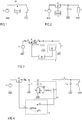
Figure 1 is a schematic diagram of a circuit including a load switch for disconnecting a load. -
Figure 2 is a schematic diagram of another circuit including a load switch for disconnecting a load. -
Figure 3 illustrates a schematic diagram of a circuit for managing an inrush current. -
Figure 4 illustrates a schematic diagram of another circuit for managing an inrush current. -
Figure 5 illustrates a circuit for managing an inrush current. -
Figure 6 illustrates in timing diagrams several voltages and currents within the circuit ofFigure 5 . -
Figure 7 illustrates in timing diagrams several further voltages within the circuit ofFigure 5 . -
Figure 8 illustrates in a flow chart a method for managing an inrush current. -
Figure 1 illustrates a circuit including aload 2. Theload 2 is coupled between a voltage source V1 and a terminal for a negative supply potential GND. A switch S1 is coupled between theload 2 and the voltage source V1 and is configured to connect theload 2 to or disconnect theload 2 from the voltage source V1. Acontrol unit 4 is configured to control the switch S1. Thecontrol unit 4, for example, may provide a control signal to the switch S1. Depending on the control signal, the switch S1 may be opened or closed. In one example, the switch S1 may be closed if the control signal has a high level and may be open if the control signal has a low level, or vice versa. This is, however, only an example. In another example, the switch S1 may be closed when the control signal is above a threshold level and may be opened when the control signal is below the threshold level, or vice versa. The switch S1 may be opened during time periods, during which an operation of theload 2 is not required. The circuit may be in a standby-mode, for example, when the switch S1 is open. The circuit may be in an active mode, for example, when the switch S1 is closed. Especially in circuits including battery powered loads, such load switches S1 are often used to extend battery lifetime. While connected to the battery, theload 2 usually consumes at least a small amount of power, even if theload 2 is inactive. The use of load switches can significantly reduce quiescent current. - The circuit illustrated in
Figure 2 is similar to the circuit that has been described with regard toFigure 1 . The switch S1 in the example ofFigure 2 , however, is implemented as a MOSFET (Metal Semiconductor Field-Effect Transistor). The MOSFET may be a P-channel or N-channel MOSFET that passes the voltage to theload 2, when the transistor is in an on-state. This is, however, only an example. A load switch S1 may be implemented in any other suitable way. In the circuit inFigure 2 , a load capacitor CL is coupled in parallel to theload 2 between the switch S1 and the terminal for negative supply potential GND. The capacitor CL is configured to ensure that there are no voltage drops on the supply rails. However, when power is initially applied to the system, e.g., when the switch S1 is closed to activate theload 2, this capacitor CL charges. The charging of the capacitor CL can result in an inrush current. This inrush current may be in the order of up to 100A and more. Thus, the inrush current may exceed the nominal load current. The nominal load current in this context is the maximum amount of electric current theload 2 can carry before sustaining immediate damage or deterioration. - Upon system startup (e.g., when the switch S1 is closed), the power supply V1 will ramp up to the regulated voltage. As the voltage increases, the inrush current flows into the uncharged capacitor CL. The amount of inrush current into the capacitor CL is determined by the slope of the voltage ramp described as follows:

- When the inrush current is managed or controlled, the charging of the capacitor CL becomes slower. Generally, an inrush current can be reduced by increasing the voltage rise time of the capacitor CL and thereby slowing down the rate at which the capacitor CL charges. If the voltage increases linearly, the charging current (inrush current ic) remains constant.
-
Figure 3 illustrates an example of a circuit for managing the inrush current. The circuit generally corresponds to the circuit ofFigure 2 , however thecontrol unit 4 in the circuit ofFigure 3 includes asense unit 42 and aswitching unit 44. Thecontrol unit 4 is coupled to a common node between the switch S1 and theload 2 with a first input. At its output thecontrol unit 4 provides a switching signal to the switch S1, the switching signal being configured to switch the switch S1 on or off (switch closed or open). Thesense unit 42 and the switchingunit 44 are coupled in series between the input and the output of thecontrol unit 4. Thesense unit 42 is configured to determine the inrush current ic. The switchingunit 44 is configured to control the switch S1 depending on the inrush current iC measured by thesense unit 42. In particular, the switchingunit 44 may control the turning on of the switch S1. The switch S1 may be implemented as a MOSFET, for example. In the circuit ofFigure 3 the MOSFET is illustrated as an enhancement-type MOSFET. A MOSFET generally is a voltage controlled field effect transistor. A MOSFET of the enhancement-type conducts virtually no current (ID = 0), when the gate-source voltage VGS of the MOSFET is zero. When the gate-source voltage VGS reaches a threshold voltage, a drain current ID starts flowing through the MOSFET (ID > 0). The amount of current that flows through the MOSFET is dependent on the gate-source voltage VGS. Therefore, the drain current ID and thus the resulting inrush current IC may be controlled by controlling the gate-source voltage VGS. The switchingunit 44 may be configured to control this gate-source voltage VGS. For example, the MOSFET may be operated in its so-called linear region during turn-on. In this linear region the drain-source channel (D-S) of the MOSFET is conducting and is controlled by the gate-source voltage VGS. For the MOSFET to be in the linear state the gate-source voltage VGS has to be in the range of the so-called Miller voltage. - The MOSFET may be operated in its linear region until the capacitor CL is fully charged. Operating the MOSFET in its linear region, thereby providing a constant charging current to the capacitor CL, increases the time that is needed to fully charge the capacitor CL.
-
Figure 4 illustrates another circuit for managing the inrush current. In the circuit ofFigure 4 , a first capacitor CL1 is coupled between the switch S1 and the terminal for negative supply potential GND. An inductance L1 is coupled between theload 2 and a common node between the switch S1 and the first capacitor CL1. A second capacitor CL2 is coupled in parallel to theload 2 between the inductance L1 and the terminal for negative supply potential GND. The inductance L1 and the second capacitor CL2 form an LC circuit (resonant circuit). The second capacitor CL2 may be an electrolytic capacitor, for example. The use of two load capacitors CL1, CL2 is only an example. Any other number of load capacitors CL1, CL2 may be used in the circuit, depending on the application. - The
sense unit 42 includes a sense capacitor CS and a sense resistor RS that are coupled in series. The series connection including the sense capacitor CS and the sense resistor RS is coupled in parallel to the first capacitor CL1 between the switch S1 and the terminal for negative supply potential GND. Thesense unit 42 further includes a firstoperational amplifier OpAmp 1. With a first input V1, the operational amplifier OpAmp1 is coupled to the common node between the sense resistor RS and the terminal for negative supply potential GND. With a second input V2, theoperational amplifier OpAmp 1 is coupled to a common node between the sense capacitor CS and the sense resistor RS. The operational amplifier OpAmp1 is configured to determine a sense current through the sense resistor RS. At its output VOUT1, the operational amplifier OpAmp1 provides a sense voltage that is dependent on the sense current through the sense resistor RS and, therefore, also on the inrush current iC. - The switching
unit 44 includes a second operational amplifier OpAmp2. At a first input V3, the second operational amplifier OpAmp2 receives the sense voltage from the first operational amplifier OpAmp1. At a second input V4, the second operational amplifier OpAmp2 receives a reference voltage. The second operational amplifier OpAmp2 is configured to provide a switching voltage at its output VOUT2 that is provided to the gate G of the MOSFET. The switching voltage depends on the difference between the sense voltage and the reference voltage. When the sense voltage is lower than the reference voltage, a switching voltage will be provided to the gate G of the MOSFET. Once the gate-source voltage VGS is greater than the threshold voltage of the MOSFET, the MOSFET conducts a current, as has been explained above. As a result, the gate-source voltage VGS decreases when the inrush current ic increases, and vice versa. When the gate-source voltage VGS decreases, this will also result in a decrease of the inrush current iC. In this way the inrush current iC can be controlled to not exceed a predetermined value. - The general function of the circuit for managing the inrush current is further described referring to
Figure 5 , which illustrates a simulation circuit for managing the inrush current. The circuit includes capacitors C2, C3 and C4 at the input of theload 2. The input switch (S1 inFigures 1 - 4 ) in the circuit ofFigure 5 includes 4 MOSFETs M2, M4, M5, M6. A sense capacitor C5 and a sense resistance R3 are configured to determine the inrush current, as has been explained with regard toFigure 4 . The operational amplifier U1 corresponds to the first operational amplifier OpAmp1 ofFigure 4 . The input switch M2, M4, M5, M6 is controlled by a further operational amplifier that is formed by transistors Q15 and Q16. The reference voltage of this further operational amplifier Q15, Q16 is provided by the Zener diode D2 that is coupled between one of the transistors Q15 and the terminal for negative supply potential GND. - If, e.g., R9 = 20kΩ and R4 = 10Ω, then the gain of operational amplifier U1 will be U1 = R9/R4 = 20kΩ/10Ω = 2000. The additional operational amplifier Q15, Q16 maintains the output of operational amplifier U1 equal to its reference, e.g. 3V. For an output voltage of 3V and a gain of 2000, the second input voltage for operational amplifier U1 may be calculated as 3V/2000 = 1.5mV. A current through resistor R3, therefore, maybe calculated as 1.5mV/0.1Ω = 15mA, if R3 = 0.1Ω. This current is the constant current which charges capacitor C5 to the input rail voltage. The time that is required to charge capacitor C5 at a constant current of 15mA may be calculated as T = C ∗ V/I and, therefore, if C5 = 4.7µF, T = 4.7
µF ∗ 13V / 15mA = 4ms. This means that it will take 4ms to charge capacitor C5 at a constant current of 15mA. The charging current, which corresponds to the inrush current, may generally be calculated as I = C ∗ V/T. Therefore, if C2 = C3 = C4 = 560µF, iC =560µF ∗ 3 ∗ 13V / 4ms = 5.5A. The values in this example, however, are only exemplarily chosen. Any other suitable values may be chosen for the components within a circuit for managing the inrush current. - It can be seen from the results described above that even if supply rail (node KL30) rises sharply, the voltage at the electrolytic capacitors C3, C4, C5 (node KL30_SW) rises much more slowly. The time that is needed to fully charge the capacitors C3, C4, C5 (rise time at node KL30_SW) is about 4ms, as has been calculated above. The charging current through resistor R1 is about 5.5A. The output of operational amplifier U1 is maintained at about 3V. During the 4ms that are needed to charge the capacitors C3, C4, C5, the MOSFETs M2, M4, M5, M6 are driven in their linear region and, therefore, limit the inrush current. In the current example this can be seen as a voltage of about 3V at the GATE of the MOSFETs M2, M4, M5, M6. When, after about 4ms the capacitors C2, C3, C4 are fully charged, the output of the operational amplifier U1 reduces and the further operational amplifier Q15, Q16 increases its output voltage, trying to maintain the output of operational amplifier U1 equal to the reference voltage. This increases the gate-source voltage of the MOSFETs M2, M4, M5, M6 and turns the MOSFETs M2, M4, M5, M6 fully on. These results demonstrate that as a result the voltage between nodes KL30 and KL30_SW reduces slowly (while the MOSFETs M2, M4, M5, M6 are in linear mode) and finally reaches zero after about 4ms when the capacitors C2, C3, C4 are fully charged (MOSFETs M2, M4, M5, M6 are fully on).
- This is further illustrated in the diagrams in
Figures 6 and7 . The first diagram inFigure 6 (topmost diagram) illustrates the voltage at node KL30 (V(KL30)) over time. As can be seen, the voltage V(KL30) immediately rises to a maximum voltage, which is about 13V in the circuit ofFigure 5 . The voltage at node KL30_SW (second diagram from top), however, is regulated and rises linearly for about 4ms until the capacitors C2, C3, C4 are fully charged. When the capacitors C2, C3, C4 are fully charged, the voltage V(KL30_SW) reaches its maximum value at about 13V. The current I(R1) at resistor R1 (third diagram from top) shows a peak shortly after the voltage at node KL30 rises to its maximum value and then stays constant at a value of about 5.6A until the capacitors C2, C3, C4 are fully charged. When, after about 4ms, the capacitors C2, C3, C4 are fully charged, the current I(R1) falls back to 0A. The voltage V(OUT) at the output of operational amplifier U1, after a short peak, levels to a value of about 3.0V until the capacitors C2, C3, C4 are fully charged, when it falls back to zero. -
Figure 7 illustrates again the voltage V(KL30_SW) at node KL30_SW (topmost diagram) and the voltage V(OUT) at the output of operational amplifier U1, as described above (second diagram from top). The voltage V(GATE) at node V(GATE, SOURCE) between the gate terminal G and the source terminal S of the MOSFET (third diagram from top) rises to about 3V (level of Miller voltage of MOSFET) while the capacitors C2, C3, C4 are charged (linear mode of MOSFETs M2, M4, M5, M6). When the capacitors C2, C3, C4 are fully charged, the voltage V(GATE) at node GATE rises to its maximum value of about 13V. The voltage V(KL30, KL30_SW) (fourth diagram from top) between node KL30 and node KL30_SW in contrast, rises to a maximum value of about 13V directly after the voltage at KL30 rises to its maximum value and decreases to zero while the capacitors C2, C3, C4 are charged. -
Figure 8 illustrates in a flow chart a method for managing an inrush current. A switching signal is provided to a switch (step 800). The switch is coupled between a load and a voltage source and is configured to connect the load to or disconnect the load from the voltage source. When the load is connected to the voltage source, a current is provided to the load and the circuit is in an active mode. When the switch is open and the load is not connected to the voltage source, no current is provided to the load and the circuit is in an inactive or standby-mode. When the switch is closed, an inrush current through the switch arises. This inrush current is determined (step 802). Depending on the determined inrush current, the switching signal is adjusted (step 804). In this way, the current through the switch can be controlled and an excessive inrush current can be prevented. - While various embodiments of the invention have been described, it will be apparent to those of ordinary skill in the art that many more embodiments and implementations are possible within the scope of the invention, which is solely defined by the appended claims.
Claims (7)
- A circuit for managing an inrush current (ic) of a load (2), wherein the load (2) is coupled between a voltage source (V1) and a terminal for a negative supply potential (GND), the circuit comprising:a switch (S1) coupled between the voltage source (V1) and the load (2), and configured to connect the load (2) to or disconnect the load (2) from the voltage source (V1);at least one load capacitor (CL) coupled in parallel to the load (2) between the switch (S1) and the terminal for negative supply potential (GND); anda control unit (4), whereinthe control unit (4) comprises a sense unit (42) and a switching unit (44),the sense unit (42) is configured to determine the inrush current (ic) when the switch (S1) is closed to connect the load (2) to the voltage source (VI),the switching unit (44) is configured to control the switching of the switch (S1) depending on the inrush current (ic), characterised in thatthe sense unit (42) comprises a sense resistor (Rs), a sense capacitor (Cs), and a first operational amplifier (OpAmp1),the sense resistor (Rs) and the sense capacitor (Cs) are coupled in series between the switch (S1) and the terminal for negative supply potential (GND), in parallel to the load (2); andthe first operational amplifier (OpAmp1) is configured to determine a current through the sense resistor (Rs) and to provide a sense voltage, wherein the current through the sense resistor (Rs) depends on the inrush current and the sense voltage depends on the current through the sense resistor (Rs).
- The circuit of claim 1, wherein the switch (S1) comprises at least one MOSFET.
- The circuit of claim 1 or 2, wherein the switching unit (44) comprises a second operational amplifier (OpAmp2), wherein the second operational amplifier (OpAmp2) is configured to provide a switching voltage to the switch (S1).
- The circuit of claim 3, wherein the switching voltage depends on a difference between the sense voltage provided by the first operational amplifier (OpAmp1) and a reference voltage.
- A method for managing an inrush current (ic) of a load (2), wherein the load (2) is coupled between a voltage source (V1) and a terminal for a negative supply potential (GND), the method comprising:providing a switching signal to a switch (S1), wherein the switch (S1) is coupled between the voltage source (V1) and the load (2) and wherein the switch (S1) is configured to connect the load (2) to or disconnect the load (2) from the voltage source (V1);determining an inrush current (ic) through the switch (S1) by means of a sense unit (42) of a control unit (4); andadjusting the switching signal depending on the determined inrush current (ic) by means of a switching unit (44) of the control unit (4), characterised in thatthe sense unit (42) comprises a sense resistor (Rs), a sense capacitor (Cs), and a first operational amplifier (OpAmp1),the sense resistor (Rs) and the sense capacitor (Cs) are coupled in series between the switch (S1) and the terminal for negative supply potential (GND), in parallel to the load (2); andthe method further comprises determining, by means of the first operational amplifier (OpAmp1), a current through the sense resistor (Rs) and providing a sense voltage, wherein the current through the sense resistor (Rs) depends on the inrush current and the sense voltage depends on the current through the sense resistor (Rs).
- The method of claim 5, wherein the switch (S1) includes at least one MOSFET having a gate terminal (G), a drain terminal (D) and a source terminal (S), and wherein the switching signal is configured to regulate a gate-source voltage (VGS) of the at least one MOSFET.
- The method of claim 6, wherein at least one load capacitance (CL) is coupled in parallel to the load (2) between the switch (S1) and the terminal for negative supply potential (GND), wherein the at least one load capacitance (CL) is charged when the switch (S1) closes and connects the load (2) and the at least one load capacitance (CL) to the voltage source (VI), and wherein the method further comprises operating the at least one MOSFET in its linear region from a point in time when the switch (S1) closes, until the at least one load capacitance (CL) is fully charged.
Applications Claiming Priority (2)
| Application Number | Priority Date | Filing Date | Title |
|---|---|---|---|
| EP16200617 | 2016-11-25 | ||
| PCT/EP2017/077537 WO2018095692A1 (en) | 2016-11-25 | 2017-10-27 | Circuit and method for managing an inrush current |
Publications (2)
| Publication Number | Publication Date |
|---|---|
| EP3545597A1 EP3545597A1 (en) | 2019-10-02 |
| EP3545597B1 true EP3545597B1 (en) | 2020-07-01 |
Family
ID=57406100
Family Applications (1)
| Application Number | Title | Priority Date | Filing Date |
|---|---|---|---|
| EP17793629.1A Active EP3545597B1 (en) | 2016-11-25 | 2017-10-27 | Circuit and method for managing an inrush current |
Country Status (4)
| Country | Link |
|---|---|
| US (1) | US11146059B2 (en) |
| EP (1) | EP3545597B1 (en) |
| CN (1) | CN110024250B (en) |
| WO (1) | WO2018095692A1 (en) |
Families Citing this family (3)
| Publication number | Priority date | Publication date | Assignee | Title |
|---|---|---|---|---|
| US10923909B2 (en) * | 2018-07-06 | 2021-02-16 | Te Connectivity Corporation | Inrush limiter for bidirectional solid state switches |
| CN112271800A (en) * | 2020-10-16 | 2021-01-26 | 珠海格力电器股份有限公司 | A power supply circuit and power management system without a charging circuit |
| CN119496491A (en) | 2023-08-18 | 2025-02-21 | 台达电子工业股份有限公司 | Switch trigger that suppresses inrush current |
Family Cites Families (11)
| Publication number | Priority date | Publication date | Assignee | Title |
|---|---|---|---|---|
| US5844440A (en) | 1996-12-20 | 1998-12-01 | Ericsson, Inc. | Circuit for inrush and current limiting |
| US5973419A (en) * | 1997-09-23 | 1999-10-26 | International Business Machines Corporation | Circuit and method of operation to control in-rush current and maintain power supply voltage to peripheral devices in an information system |
| JP3563333B2 (en) * | 2000-08-04 | 2004-09-08 | Necエレクトロニクス株式会社 | High-side switch for inrush current and overcurrent control method |
| US7019583B2 (en) | 2001-01-29 | 2006-03-28 | Axiohm Transaction Solutions, Inc. | Current inrush limiting circuit |
| US7542258B2 (en) | 2004-01-16 | 2009-06-02 | Lutron Electronics Co., Inc. | DV/dt-detecting overcurrent protection circuit for power supply |
| US20120063045A1 (en) * | 2010-09-10 | 2012-03-15 | Intersil Americas Inc. | Detecting and selectively ignoring power supply transients |
| CN202455301U (en) * | 2012-02-24 | 2012-09-26 | 江苏煌明能源科技有限公司 | Program-control energy-saving device for motor |
| CN103441482A (en) | 2013-08-01 | 2013-12-11 | 中国航天科技集团公司第九研究院第七七一研究所 | Current monitoring circuit with accurate current-limit function |
| US20160164279A1 (en) | 2014-12-09 | 2016-06-09 | Infineon Technologies Ag | Circuit and method for measuring a current |
| CN204668906U (en) | 2015-03-20 | 2015-09-23 | 华立仪表集团股份有限公司 | Load over-current protection circuit, the exploratory current foldback circuit of electric power acquisition equipment |
| CN205248784U (en) * | 2015-11-12 | 2016-05-18 | 贵州航天凯山石油仪器有限公司 | An overcurrent protection device for a submersible electric pump test system |
-
2017
- 2017-10-27 US US16/462,378 patent/US11146059B2/en active Active
- 2017-10-27 WO PCT/EP2017/077537 patent/WO2018095692A1/en not_active Ceased
- 2017-10-27 CN CN201780072839.8A patent/CN110024250B/en active Active
- 2017-10-27 EP EP17793629.1A patent/EP3545597B1/en active Active
Non-Patent Citations (1)
| Title |
|---|
| None * |
Also Published As
| Publication number | Publication date |
|---|---|
| US20190280477A1 (en) | 2019-09-12 |
| WO2018095692A1 (en) | 2018-05-31 |
| CN110024250A (en) | 2019-07-16 |
| US11146059B2 (en) | 2021-10-12 |
| CN110024250B (en) | 2021-11-23 |
| EP3545597A1 (en) | 2019-10-02 |
Similar Documents
| Publication | Publication Date | Title |
|---|---|---|
| US8742834B2 (en) | Negative-voltage charge pump circuit | |
| JP5851821B2 (en) | Charge / discharge control circuit and battery device | |
| TWI652490B (en) | System, circuit and method for detecting faults in hot plug applications | |
| US9118238B2 (en) | Charge pump systems with adjustable frequency control | |
| JP2021040482A (en) | Overcurrent protection device | |
| US10715027B2 (en) | Driver circuit | |
| US11239836B2 (en) | Low resistive load switch with output current control | |
| KR20150075034A (en) | Switching regulator and electronic apparatus | |
| US8283808B2 (en) | Switch arrangement and method for electrical switching | |
| US9627962B2 (en) | Fast blocking switch | |
| US8508901B2 (en) | Overcurrent detection circuit | |
| US9787180B2 (en) | High side switch with current limit feedback | |
| EP3545597B1 (en) | Circuit and method for managing an inrush current | |
| US20160187900A1 (en) | Voltage regulator circuit and method for limiting inrush current | |
| JP2024068841A (en) | Linear Regulators | |
| US7660090B1 (en) | Apparatus and method for input voltage transient protection with a low-voltage reset circuit | |
| US7830168B2 (en) | Temperature variance nullification in an inrush current suppression circuit | |
| JP7309987B2 (en) | Driver circuits for output transistors, semiconductor devices, automobiles | |
| US10459465B2 (en) | Power-down discharger | |
| EP2846211A1 (en) | Reduction in on-resistance in pass device | |
| US9059703B2 (en) | Switch circuit | |
| JP2010074874A (en) | Rush current control circuit | |
| JP7132063B2 (en) | Driver circuits for output transistors, semiconductor devices, automobiles | |
| US20250362699A1 (en) | Load drive circuit | |
| US10691151B2 (en) | Devices and methods for dynamic overvoltage protection in regulators |
Legal Events
| Date | Code | Title | Description |
|---|---|---|---|
| STAA | Information on the status of an ep patent application or granted ep patent |
Free format text: STATUS: UNKNOWN |
|
| STAA | Information on the status of an ep patent application or granted ep patent |
Free format text: STATUS: THE INTERNATIONAL PUBLICATION HAS BEEN MADE |
|
| PUAI | Public reference made under article 153(3) epc to a published international application that has entered the european phase |
Free format text: ORIGINAL CODE: 0009012 |
|
| STAA | Information on the status of an ep patent application or granted ep patent |
Free format text: STATUS: REQUEST FOR EXAMINATION WAS MADE |
|
| 17P | Request for examination filed |
Effective date: 20190418 |
|
| AK | Designated contracting states |
Kind code of ref document: A1 Designated state(s): AL AT BE BG CH CY CZ DE DK EE ES FI FR GB GR HR HU IE IS IT LI LT LU LV MC MK MT NL NO PL PT RO RS SE SI SK SM TR |
|
| AX | Request for extension of the european patent |
Extension state: BA ME |
|
| DAV | Request for validation of the european patent (deleted) | ||
| DAX | Request for extension of the european patent (deleted) | ||
| GRAP | Despatch of communication of intention to grant a patent |
Free format text: ORIGINAL CODE: EPIDOSNIGR1 |
|
| STAA | Information on the status of an ep patent application or granted ep patent |
Free format text: STATUS: GRANT OF PATENT IS INTENDED |
|
| INTG | Intention to grant announced |
Effective date: 20200424 |
|
| GRAS | Grant fee paid |
Free format text: ORIGINAL CODE: EPIDOSNIGR3 |
|
| GRAA | (expected) grant |
Free format text: ORIGINAL CODE: 0009210 |
|
| STAA | Information on the status of an ep patent application or granted ep patent |
Free format text: STATUS: THE PATENT HAS BEEN GRANTED |
|
| AK | Designated contracting states |
Kind code of ref document: B1 Designated state(s): AL AT BE BG CH CY CZ DE DK EE ES FI FR GB GR HR HU IE IS IT LI LT LU LV MC MK MT NL NO PL PT RO RS SE SI SK SM TR |
|
| REG | Reference to a national code |
Ref country code: CH Ref legal event code: EP Ref country code: AT Ref legal event code: REF Ref document number: 1287053 Country of ref document: AT Kind code of ref document: T Effective date: 20200715 |
|
| REG | Reference to a national code |
Ref country code: IE Ref legal event code: FG4D |
|
| REG | Reference to a national code |
Ref country code: DE Ref legal event code: R096 Ref document number: 602017019144 Country of ref document: DE |
|
| REG | Reference to a national code |
Ref country code: LT Ref legal event code: MG4D |
|
| PG25 | Lapsed in a contracting state [announced via postgrant information from national office to epo] |
Ref country code: BG Free format text: LAPSE BECAUSE OF FAILURE TO SUBMIT A TRANSLATION OF THE DESCRIPTION OR TO PAY THE FEE WITHIN THE PRESCRIBED TIME-LIMIT Effective date: 20201001 |
|
| REG | Reference to a national code |
Ref country code: NL Ref legal event code: MP Effective date: 20200701 |
|
| REG | Reference to a national code |
Ref country code: AT Ref legal event code: MK05 Ref document number: 1287053 Country of ref document: AT Kind code of ref document: T Effective date: 20200701 |
|
| PG25 | Lapsed in a contracting state [announced via postgrant information from national office to epo] |
Ref country code: CZ Free format text: LAPSE BECAUSE OF FAILURE TO SUBMIT A TRANSLATION OF THE DESCRIPTION OR TO PAY THE FEE WITHIN THE PRESCRIBED TIME-LIMIT Effective date: 20200701 Ref country code: FI Free format text: LAPSE BECAUSE OF FAILURE TO SUBMIT A TRANSLATION OF THE DESCRIPTION OR TO PAY THE FEE WITHIN THE PRESCRIBED TIME-LIMIT Effective date: 20200701 Ref country code: AT Free format text: LAPSE BECAUSE OF FAILURE TO SUBMIT A TRANSLATION OF THE DESCRIPTION OR TO PAY THE FEE WITHIN THE PRESCRIBED TIME-LIMIT Effective date: 20200701 Ref country code: SE Free format text: LAPSE BECAUSE OF FAILURE TO SUBMIT A TRANSLATION OF THE DESCRIPTION OR TO PAY THE FEE WITHIN THE PRESCRIBED TIME-LIMIT Effective date: 20200701 Ref country code: NO Free format text: LAPSE BECAUSE OF FAILURE TO SUBMIT A TRANSLATION OF THE DESCRIPTION OR TO PAY THE FEE WITHIN THE PRESCRIBED TIME-LIMIT Effective date: 20201001 Ref country code: PT Free format text: LAPSE BECAUSE OF FAILURE TO SUBMIT A TRANSLATION OF THE DESCRIPTION OR TO PAY THE FEE WITHIN THE PRESCRIBED TIME-LIMIT Effective date: 20201102 Ref country code: GR Free format text: LAPSE BECAUSE OF FAILURE TO SUBMIT A TRANSLATION OF THE DESCRIPTION OR TO PAY THE FEE WITHIN THE PRESCRIBED TIME-LIMIT Effective date: 20201002 Ref country code: LT Free format text: LAPSE BECAUSE OF FAILURE TO SUBMIT A TRANSLATION OF THE DESCRIPTION OR TO PAY THE FEE WITHIN THE PRESCRIBED TIME-LIMIT Effective date: 20200701 Ref country code: ES Free format text: LAPSE BECAUSE OF FAILURE TO SUBMIT A TRANSLATION OF THE DESCRIPTION OR TO PAY THE FEE WITHIN THE PRESCRIBED TIME-LIMIT Effective date: 20200701 Ref country code: HR Free format text: LAPSE BECAUSE OF FAILURE TO SUBMIT A TRANSLATION OF THE DESCRIPTION OR TO PAY THE FEE WITHIN THE PRESCRIBED TIME-LIMIT Effective date: 20200701 |
|
| PG25 | Lapsed in a contracting state [announced via postgrant information from national office to epo] |
Ref country code: PL Free format text: LAPSE BECAUSE OF FAILURE TO SUBMIT A TRANSLATION OF THE DESCRIPTION OR TO PAY THE FEE WITHIN THE PRESCRIBED TIME-LIMIT Effective date: 20200701 Ref country code: RS Free format text: LAPSE BECAUSE OF FAILURE TO SUBMIT A TRANSLATION OF THE DESCRIPTION OR TO PAY THE FEE WITHIN THE PRESCRIBED TIME-LIMIT Effective date: 20200701 Ref country code: LV Free format text: LAPSE BECAUSE OF FAILURE TO SUBMIT A TRANSLATION OF THE DESCRIPTION OR TO PAY THE FEE WITHIN THE PRESCRIBED TIME-LIMIT Effective date: 20200701 Ref country code: IS Free format text: LAPSE BECAUSE OF FAILURE TO SUBMIT A TRANSLATION OF THE DESCRIPTION OR TO PAY THE FEE WITHIN THE PRESCRIBED TIME-LIMIT Effective date: 20201101 |
|
| PG25 | Lapsed in a contracting state [announced via postgrant information from national office to epo] |
Ref country code: NL Free format text: LAPSE BECAUSE OF FAILURE TO SUBMIT A TRANSLATION OF THE DESCRIPTION OR TO PAY THE FEE WITHIN THE PRESCRIBED TIME-LIMIT Effective date: 20200701 |
|
| REG | Reference to a national code |
Ref country code: DE Ref legal event code: R097 Ref document number: 602017019144 Country of ref document: DE |
|
| PG25 | Lapsed in a contracting state [announced via postgrant information from national office to epo] |
Ref country code: DK Free format text: LAPSE BECAUSE OF FAILURE TO SUBMIT A TRANSLATION OF THE DESCRIPTION OR TO PAY THE FEE WITHIN THE PRESCRIBED TIME-LIMIT Effective date: 20200701 Ref country code: RO Free format text: LAPSE BECAUSE OF FAILURE TO SUBMIT A TRANSLATION OF THE DESCRIPTION OR TO PAY THE FEE WITHIN THE PRESCRIBED TIME-LIMIT Effective date: 20200701 Ref country code: EE Free format text: LAPSE BECAUSE OF FAILURE TO SUBMIT A TRANSLATION OF THE DESCRIPTION OR TO PAY THE FEE WITHIN THE PRESCRIBED TIME-LIMIT Effective date: 20200701 Ref country code: IT Free format text: LAPSE BECAUSE OF FAILURE TO SUBMIT A TRANSLATION OF THE DESCRIPTION OR TO PAY THE FEE WITHIN THE PRESCRIBED TIME-LIMIT Effective date: 20200701 Ref country code: SM Free format text: LAPSE BECAUSE OF FAILURE TO SUBMIT A TRANSLATION OF THE DESCRIPTION OR TO PAY THE FEE WITHIN THE PRESCRIBED TIME-LIMIT Effective date: 20200701 |
|
| PLBE | No opposition filed within time limit |
Free format text: ORIGINAL CODE: 0009261 |
|
| STAA | Information on the status of an ep patent application or granted ep patent |
Free format text: STATUS: NO OPPOSITION FILED WITHIN TIME LIMIT |
|
| PG25 | Lapsed in a contracting state [announced via postgrant information from national office to epo] |
Ref country code: AL Free format text: LAPSE BECAUSE OF FAILURE TO SUBMIT A TRANSLATION OF THE DESCRIPTION OR TO PAY THE FEE WITHIN THE PRESCRIBED TIME-LIMIT Effective date: 20200701 |
|
| REG | Reference to a national code |
Ref country code: CH Ref legal event code: PL |
|
| 26N | No opposition filed |
Effective date: 20210406 |
|
| PG25 | Lapsed in a contracting state [announced via postgrant information from national office to epo] |
Ref country code: LU Free format text: LAPSE BECAUSE OF NON-PAYMENT OF DUE FEES Effective date: 20201027 Ref country code: MC Free format text: LAPSE BECAUSE OF FAILURE TO SUBMIT A TRANSLATION OF THE DESCRIPTION OR TO PAY THE FEE WITHIN THE PRESCRIBED TIME-LIMIT Effective date: 20200701 Ref country code: SK Free format text: LAPSE BECAUSE OF FAILURE TO SUBMIT A TRANSLATION OF THE DESCRIPTION OR TO PAY THE FEE WITHIN THE PRESCRIBED TIME-LIMIT Effective date: 20200701 |
|
| REG | Reference to a national code |
Ref country code: BE Ref legal event code: MM Effective date: 20201031 |
|
| PG25 | Lapsed in a contracting state [announced via postgrant information from national office to epo] |
Ref country code: FR Free format text: LAPSE BECAUSE OF NON-PAYMENT OF DUE FEES Effective date: 20201031 |
|
| PG25 | Lapsed in a contracting state [announced via postgrant information from national office to epo] |
Ref country code: SI Free format text: LAPSE BECAUSE OF FAILURE TO SUBMIT A TRANSLATION OF THE DESCRIPTION OR TO PAY THE FEE WITHIN THE PRESCRIBED TIME-LIMIT Effective date: 20200701 Ref country code: LI Free format text: LAPSE BECAUSE OF NON-PAYMENT OF DUE FEES Effective date: 20201031 Ref country code: CH Free format text: LAPSE BECAUSE OF NON-PAYMENT OF DUE FEES Effective date: 20201031 Ref country code: BE Free format text: LAPSE BECAUSE OF NON-PAYMENT OF DUE FEES Effective date: 20201031 |
|
| PG25 | Lapsed in a contracting state [announced via postgrant information from national office to epo] |
Ref country code: IE Free format text: LAPSE BECAUSE OF NON-PAYMENT OF DUE FEES Effective date: 20201027 |
|
| PG25 | Lapsed in a contracting state [announced via postgrant information from national office to epo] |
Ref country code: TR Free format text: LAPSE BECAUSE OF FAILURE TO SUBMIT A TRANSLATION OF THE DESCRIPTION OR TO PAY THE FEE WITHIN THE PRESCRIBED TIME-LIMIT Effective date: 20200701 Ref country code: MT Free format text: LAPSE BECAUSE OF FAILURE TO SUBMIT A TRANSLATION OF THE DESCRIPTION OR TO PAY THE FEE WITHIN THE PRESCRIBED TIME-LIMIT Effective date: 20200701 Ref country code: CY Free format text: LAPSE BECAUSE OF FAILURE TO SUBMIT A TRANSLATION OF THE DESCRIPTION OR TO PAY THE FEE WITHIN THE PRESCRIBED TIME-LIMIT Effective date: 20200701 |
|
| PG25 | Lapsed in a contracting state [announced via postgrant information from national office to epo] |
Ref country code: MK Free format text: LAPSE BECAUSE OF FAILURE TO SUBMIT A TRANSLATION OF THE DESCRIPTION OR TO PAY THE FEE WITHIN THE PRESCRIBED TIME-LIMIT Effective date: 20200701 |
|
| P01 | Opt-out of the competence of the unified patent court (upc) registered |
Effective date: 20230526 |
|
| PGFP | Annual fee paid to national office [announced via postgrant information from national office to epo] |
Ref country code: GB Payment date: 20250923 Year of fee payment: 9 |
|
| PGFP | Annual fee paid to national office [announced via postgrant information from national office to epo] |
Ref country code: DE Payment date: 20250923 Year of fee payment: 9 |