EP3544178A1 - Amplifier device with harmonic termination circuit - Google Patents
Amplifier device with harmonic termination circuit Download PDFInfo
- Publication number
- EP3544178A1 EP3544178A1 EP19158596.7A EP19158596A EP3544178A1 EP 3544178 A1 EP3544178 A1 EP 3544178A1 EP 19158596 A EP19158596 A EP 19158596A EP 3544178 A1 EP3544178 A1 EP 3544178A1
- Authority
- EP
- European Patent Office
- Prior art keywords
- terminal
- coupled
- input
- transistor
- circuit
- Prior art date
- Legal status (The legal status is an assumption and is not a legal conclusion. Google has not performed a legal analysis and makes no representation as to the accuracy of the status listed.)
- Withdrawn
Links
Images




Classifications
-
- H—ELECTRICITY
- H03—ELECTRONIC CIRCUITRY
- H03F—AMPLIFIERS
- H03F1/00—Details of amplifiers with only discharge tubes, only semiconductor devices or only unspecified devices as amplifying elements
- H03F1/02—Modifications of amplifiers to raise the efficiency, e.g. gliding Class A stages, use of an auxiliary oscillation
- H03F1/0205—Modifications of amplifiers to raise the efficiency, e.g. gliding Class A stages, use of an auxiliary oscillation in transistor amplifiers
- H03F1/0288—Modifications of amplifiers to raise the efficiency, e.g. gliding Class A stages, use of an auxiliary oscillation in transistor amplifiers using a main and one or several auxiliary peaking amplifiers whereby the load is connected to the main amplifier using an impedance inverter, e.g. Doherty amplifiers
-
- H—ELECTRICITY
- H03—ELECTRONIC CIRCUITRY
- H03F—AMPLIFIERS
- H03F1/00—Details of amplifiers with only discharge tubes, only semiconductor devices or only unspecified devices as amplifying elements
- H03F1/56—Modifications of input or output impedances, not otherwise provided for
- H03F1/565—Modifications of input or output impedances, not otherwise provided for using inductive elements
-
- H—ELECTRICITY
- H03—ELECTRONIC CIRCUITRY
- H03F—AMPLIFIERS
- H03F3/00—Amplifiers with only discharge tubes or only semiconductor devices as amplifying elements
- H03F3/189—High-frequency amplifiers, e.g. radio frequency amplifiers
- H03F3/19—High-frequency amplifiers, e.g. radio frequency amplifiers with semiconductor devices only
- H03F3/195—High-frequency amplifiers, e.g. radio frequency amplifiers with semiconductor devices only in integrated circuits
-
- H—ELECTRICITY
- H03—ELECTRONIC CIRCUITRY
- H03F—AMPLIFIERS
- H03F2200/00—Indexing scheme relating to amplifiers
- H03F2200/222—A circuit being added at the input of an amplifier to adapt the input impedance of the amplifier
-
- H—ELECTRICITY
- H03—ELECTRONIC CIRCUITRY
- H03F—AMPLIFIERS
- H03F2200/00—Indexing scheme relating to amplifiers
- H03F2200/387—A circuit being added at the output of an amplifier to adapt the output impedance of the amplifier
-
- H—ELECTRICITY
- H03—ELECTRONIC CIRCUITRY
- H03F—AMPLIFIERS
- H03F2200/00—Indexing scheme relating to amplifiers
- H03F2200/423—Amplifier output adaptation especially for transmission line coupling purposes, e.g. impedance adaptation
-
- H—ELECTRICITY
- H03—ELECTRONIC CIRCUITRY
- H03F—AMPLIFIERS
- H03F2203/00—Indexing scheme relating to amplifiers with only discharge tubes or only semiconductor devices as amplifying elements covered by H03F3/00
- H03F2203/20—Indexing scheme relating to power amplifiers, e.g. Class B amplifiers, Class C amplifiers
- H03F2203/21—Indexing scheme relating to power amplifiers, e.g. Class B amplifiers, Class C amplifiers with semiconductor devices only
- H03F2203/211—Indexing scheme relating to power amplifiers, e.g. Class B amplifiers, Class C amplifiers with semiconductor devices only using a combination of several amplifiers
- H03F2203/21139—An impedance adaptation circuit being added at the output of a power amplifier stage
Definitions
- Embodiments of the subject matter described herein relate generally to RF amplifiers.
- High-efficiency radio-frequency (RF) amplifiers are finding increased use in communication base station applications. These high-efficiency RF amplifiers are desired because of the lower system size and cost achieved by the need for less cooling capability and because of the reduced energy needed to power these systems.
- Conventional high efficiency amplifiers e.g. tuned class-AB
- This high efficiency operation is achieved by terminating the active transistor of the amplifier at the harmonic frequencies of the frequency of amplifier operation.
- an ideal tuned class-clAB amplifier may require all harmonics to be terminated in a short circuit.
- An ideal class-F amplifier may require terminating the even harmonics (i.e. 2 nd , 4 th , etc.) of the amplifier signal in a short circuit and the odd harmonics (i.e. 3 rd , 5 th , etc.) of the amplifier signal in an open circuit.
- Various embodiments of the inventive subject matter include an input terminal, an output terminal, a first transistor and a class-J circuit coupled between the first transistor and the output terminal and configured to harmonically terminate the first transistor.
- the class-J circuit may include a first resonator, characterized by a first resonant frequency substantially equal to a second harmonic frequency.
- the first resonator may be coupled between the second current-carrying terminal and a voltage reference.
- a shunt inductor that is distinct from the first resonator may be coupled between the second current-carrying terminal and the voltage reference.
- the amplifier device embodiments provided herein may overcome some or all of the aforementioned issues with high-efficiency amplifiers, while realizing these amplifiers in a compact form factor. Specifically, the amplifier device embodiments described herein efficiently terminate the harmonics frequency components of the amplifier signal, making the amplifier less sensitive to changes in harmonic tuning conditions outside the amplifier device.
- Class-J amplification provides high efficiency amplification similar to tuned class-AB amplification, but is easier to realize with practical circuit elements.
- class-J circuits do not require termination of harmonics in in ideal short circuits as is the case for tuned class-AB amplifiers. Rather, the transistor may be terminated with capacitive reactances.
- FIG. 1 is a simplified block diagram of an amplifier device 100, in accordance with an example embodiment.
- the amplifier device 100 may include a base substrate 101, an input terminal 102, an output terminal 104, an input matching circuit 110, and input harmonic termination circuit 130, a first transistor 150, a class-J circuit 170, and an output matching circuit 180.
- an RF signal received through the input terminal 102 is conveyed through the input matching circuit 110, which is configured to raise the impedance of amplifier device 100 to a higher impedance level (e.g., 50 Ohms or another impedance level) to enhance gain flatness and power transfer across the frequency band.
- the resulting RF signal is then filtered by the input harmonic termination circuit 130 to selectively remove, e.g., the second harmonic component of the RF signal.
- the resultant RF signal is then amplified by the first transistor 150.
- the amplified RF signal produced at the output 155 of the first transistor 150 is then conveyed through the class J output harmonic termination circuit 170.
- the class-J output harmonic termination circuit 170 shapes the current and voltage wave forms by using appropriate passive fundamental and harmonic terminations which result in high efficiency operation.
- the resulting RF signal produced at the output 175 of the class-J output harmonic termination circuit 170 is then conveyed to the output matching circuit 190.
- the output impedance matching circuit 190 is connected between the class-J output and is configured to match the output impedance of the first transistor 150 with the system impedance applied to output terminal 104.
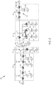
- FIG. 2 is a schematic diagram depicting amplifier device 100 of FIG. 1 , showing circuit schematic details of the amplifier device 200, in accordance with an example embodiment. More particularly, corresponding components between FIG. 1 and FIG. 2 have the same last two numerical digits (e.g., components 130 and 230 are corresponding components, and components 170 and 270 are corresponding components).
- the amplifier device 200 may include an input terminal 202, an output terminal 204, an input matching circuit 210, an input harmonic termination circuit 230, a first transistor 250, a class-J circuit 270, and an output matching circuit 290.
- components may be coupled to various circuit grounds (i.e. "voltage references").
- voltage references may be used in place of circuit grounds referred to herein.
- These alternative voltage references may include a positive or negative direct current (DC) potential or alternating current (AC) potentials.
- the input matching circuit 210 may couple the input terminal 202 to the first transistor device 250.
- the input matching circuit 210 may include one or more circuit elements configured to raise the impedance seen at the input terminal 202 and provide maximum power transfer and gain over the frequency range of the amplifier device 200.
- a plurality of matching network sections may be cascaded to realize the needed impedance matching.
- a first input T-network 211 and a double T-network 220 may be coupled together to form the input matching circuit 210.
- the first input T-network 211 may include a first input series inductor 212, a second input series inductor 213 coupled to the first input series inductor 212, and a first input shunt capacitor 214 that couples the connection point of the first input series inductor 212 and the second input series inductor 213 to a circuit ground 215.
- the first and second series inductors 212 and 213 of the first T-network 211 may have a value in a range of about 0.15 NH and about 0.55 NH, though other higher or lower values may be used.
- the first input shunt capacitor 214 may have a value in a range of about 0.1 pF and about 0.5 pF, though other higher or lower values may be used.
- the double T-network 220 may include a third input series inductor 221, a fourth input series inductor 222 coupled to the third input series inductor 221, a second input shunt capacitor 223 that couples the connection point of the third input series inductor 221 and the fourth input series inductor 222 to the circuit ground 224, a fifth input series inductor 226, and a shunt input capacitor 227 that couples the connection point of the fourth input series inductor 222 and the fifth input series inductor 226 to a circuit ground 228.
- the third input series inductor 221 of the double T-network 220 may have a value in a range of about 0.1 nH and about 0.5 nH, though other higher or lower values may be used.
- the fourth input inductor 222 may have a value in a range of about 0.1 nH and about 1.5 nH, though other higher or lower values may be used.
- the second input shunt capacitor 223 may have a value in a range of about 2 pF and about 6 pF, though other higher or lower values may be used.
- the fifth input series inductor 226 may have a value in a range of about 0.3 nH and about 1.1 nH, though other higher or lower values may be used.
- the third input shunt capacitor 227 may have a value in a range of about 6 pF and about 16 pF, though other higher or lower values may be used.
- An input harmonic termination circuit 230 may be coupled to an input harmonic termination node 232.
- the input harmonic termination circuit 230 may include an input harmonic termination resonator 233 coupled to input harmonic termination node 232.
- the input harmonic termination resonator 233 may be coupled between the input harmonic termination node 232 and a circuit ground 234.
- the input harmonic termination resonator 233 may include an input harmonic termination capacitor 236 and an input harmonic termination inductor 237, according to an embodiment.
- the input harmonic termination capacitor 236 may have a value in a range of about 0.30 pF and about 0.9 pF, though other higher or lower values may be used.
- the input harmonic termination inductor 237 may have a value in a range of about 0.4 nH and about 1.3 nH, though other higher or lower values may be used.
- the input harmonic termination resonant frequency may be substantially equal to a second harmonic frequency (e.g. 7 GHz) of the intended operating frequency of the amplifier device 200 (e.g. 3.5 GHz).
- the first transistor 250 is the primary active component of the amplifier device 200.
- the first transistor 250 may include a control terminal 252, a first current-carrying terminal 254, and a second current-carrying terminal 256, where the current-carrying terminals are spatially and electrically separated by a variable-conductivity channel.
- the first transistor 200 has an output capacitance between the first and second current-carrying terminals.
- the first transistor 250 may include field effect transistors (FET's) (such as heterojunction FET's (HFET's), metal-semiconductor FET's (MESFET's), or metal oxide semiconductor FET's (MOSFET's)), each of which include a gate (control terminal), a source (a first current-carrying terminal), and a drain (a second current-carrying terminal).
- FET's field effect transistors
- HFET's heterojunction FET's
- MESFET's metal-semiconductor FET's
- MOSFET's metal oxide semiconductor FET's
- the first transistor 250 may include a bipolar junction transistors (BJT) or a heterojunction BJT (HBT). Accordingly, references herein to a "gate,” “drain,” and “source,” are not intended to be limiting, as each of these designations has analogous features for a bipolar device implementation (e.g., a base, collector, and emitter, respectively).
- the gate terminal 252 (i.e. control terminal) may be coupled to the input harmonic termination node 232.
- the source terminal 254 (i.e. first current-carrying element) of the first transistor 250 may be coupled to a circuit ground 255 (i.e. voltage reference).
- the drain terminal 256 i.e. second current-carrying terminal
- the first transistor 250 may have a total gate width of between about 1 and about 40 millimeters (mm) (e.g. about 3.5 mm), although higher or lower values of the total gate width may be used in some embodiments.
- the first transistor 250 has an input capacitance (i.e. gate-source capacitance) between the gate terminal 252 and source 254 of the first transistor 250.
- the first transistor 250 has a gate source capacitance between about 0.5 pF per millimeter of gate periphery (pF/mm) and about 3.5 pF/mm (e.g. 2.5 pF/mm), though higher or lower values may be used.
- the first transistor 250 has an output capacitance (i.e. drain-source capacitance) between the drain terminal 256 and source terminal 254 of the first transistor 250.
- the first transistor 250 has a drain-source capacitance between about 0.2 pF per millimeter of gate periphery (pF/mm) and about 1 pF/mm (e.g. about 0.4 pF/mm), though other higher or lower values may be used.
- an active matching element e.g. a transistor stage
- FIG. 3 is a schematic diagram of an amplifier device in accordance with an alternate embodiment wherein an active matching element is incorporated into the input matching circuit.
- an input driver circuit 310 takes the place of the matching circuit 210 of FIG 2 .
- the input driver circuit may include an input match circuit 312, a second transistor 320 coupled to the input match circuit 312, and an inter-stage match circuit 325 that couples to an input harmonic termination node 332 of the input harmonic termination 331 via a DC blocking capacitor 329.
- the input match circuit 312 may include one or more low-pass (e.g. T-network), high-pass, or other suitable matching networks configured to transform the impedance of the gate terminal 322 of the second transistor 320 to the system impedance presented to input terminal 302, according to an embodiment.
- the second transistor 320 may include a GaN transistor.
- the second transistor 320 may include a laterally diffused, metal oxide semiconductor (LDMOS) transistor.
- LDMOS metal oxide semiconductor
- Other embodiments may include gallium arsenide (GaAs) devices, and silicon-germanium (SiGe) devices.
- the second transistor 320 may include analogous terminals (e.g. gate terminal 252, drain terminal 256, and source terminal 254) described in connection with the first transistor 250, FIG. 2 in accordance with an embodiment.
- the second transistor 320 may include a second transistor gate terminal 322 (i.e. "second control terminal"), an active transistor source terminal 324 (i.e. third current-carrying terminal), and an active transistor drain terminal 326 (i.e. fourth current-carrying terminal).
- the second transistor 320 may be biased in forward active-operation (e.g. class-AB bias) using a DC bias applied at the second transistor gate 322 via the input terminal 302.
- a drain bias may be applied to the drain terminal 326 of the second transistor 320 through a drain bias circuit 323.
- the RF signal may be conveyed from the output terminal 316 of the input match circuit 312 to the second transistor gate terminal 322 and an amplified version RF signal may be generated at the second transistor drain terminal 326.
- the resulting amplified RF signal may then be conveyed from the inter-stage input 327 of the inter-stage match circuit 325 to the inter-stage output 328.
- the inter-stage match circuit 325 may transform the impedance of the second transistor drain terminal 326 to match that of the gate terminal 352 of the first transistor 350, according to an embodiment.
- the amplified RF signal is then conveyed from the inter-stage output 328 to the input harmonic termination node 332 of the input harmonic termination circuit 330, according to an embodiment.
- a gate bias may be applied to the gate 352 of the first transistor 350 via a gate bias circuit 353.
- the amplifier device 300 may have the same features and functions as the amplifier device 200, according to an embodiment. In an embodiment, these features may be identical to that of amplifier device 200 of FIG. 2 and will only be described in connection with FIG. 2 for the purpose of brevity.
- the class-J circuit 270 may include a first resonator 271 and a second resonator 275, both coupled to the output harmonic termination node 279 (i.e. "first node") and coupled to the drain terminal 256 of the first transistor 250 via a series inductor 278.
- the first resonator 271 may be coupled between an output harmonic termination node 279 and a circuit ground 274.
- class-J refers to a power amplifier mode of operation wherein an output harmonic termination circuit (e.g. 170, 270, FIGs 1 , 2 ) may present an inductive impedance load at the fundamental frequency, f 0 , of the amplified signal, while at the same time, may present an impedance that includes a capacitive reactance at the harmonic frequencies of the amplified signal.
- an output harmonic termination circuit e.g. 170, 270, FIGs 1 , 2
- the inductive portion of the fundamental output load phase-shifts the drain voltage waveform seen at the drain terminal 256 of the first transistor 250 relative to the associated current waveform such that the voltage waveform leads the current waveform in phase.
- the capacitive reactance at the second harmonic frequency may cause an additional second harmonic component to cause additional peaking in the voltage waveform, beyond the 2 V DD maximum voltage swing that is well known for conventional class-AB amplifier operation where V DD refers to the supply voltage applied at the drain terminal 256 of the first transistor 250.
- the first resonator 271 may include a first output harmonic termination capacitor 272 and a first output harmonic termination inductor 273, according to an embodiment.
- the first output harmonic termination capacitor 272 may have a value in a range of about 0.15 pF and about 0.45 pF, though other higher or lower values may be used.
- the first output harmonic termination inductor 273 may have a value in a range of about 0.8 nH and about 2.4 nH, though other higher or lower values may be used.
- the first resonant frequency may be substantially equal to a second harmonic frequency of the intended operating frequency the amplifier device 200.
- a second resonator 275 may be coupled between the output harmonic termination node 279 and the circuit ground 274.
- the second resonator 275 may include a second output harmonic termination capacitor 276 and a second output harmonic termination inductor 277.
- the second output harmonic termination capacitor 276 may have a value in a range of about 0.15 pF and about 0.45 pF, though other higher or lower values may be used. In an embodiment, and for a center frequency, f 0 , of 3.5 GHz, the second output harmonic termination inductor 277 may have a value in a range of about 0.35 nH and about 1.1 nH, though other higher or lower values may be used.
- the second resonator 275 may be characterized by a second resonant frequency substantially equal to a third harmonic frequency.
- second harmonic frequency or “third harmonic frequency” refers to a frequency component of an RF signal produced at the drain terminal 256 (i.e. second current-carrying terminal and the output terminal 204), as a result of the nonlinear behavior of first transistor 250 (and possibly second transistor 320 for the alternate embodiment of FIG. 3 ), that is two (for second harmonic) or three (for third harmonic) times the frequency of a signal placed on the input terminal 202 (i.e. 2 f0 , 3 f0 ).
- the series inductor 278 of the class-J circuit 270 may be coupled to the drain terminal 256 (i.e. second current-carrying terminal) and the output harmonic termination node 279.
- the value of the series inductor 278 may be chosen such that it resonates with the output capacitance of the first transistor 250 at a frequency below the first resonant frequency (i.e. the 2 nd harmonic frequency).
- the series inductor 278 may have a value in a range of about 0.5 nH and about 1.6 nH, though other higher or lower values may be used.
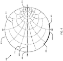
- the reflection coefficient, S 11 well known to those with skill in the art is defined as the complex ratio of a test signal b 1 reflected from an input port of a network (e.g. FIG.2 , series inductor 278) in response to an incident test signal a 1 under the assumption that all other ports (e.g. FIG. 2 , harmonic termination node 279) are matched and no reflected energy may enter these ports.
- S 11 is evaluated with the class-J circuit 270 coupled to the output matching circuit 290 at harmonic termination node 279.
- the output matching circuit 290 is terminated in a 50-ohm load.
- Trace 411 shows the reflection coefficient, Sn of the class-J harmonic termination circuit, as seen by the drain terminal 256 (i.e. second current-carrying terminal) of the first transistor 250.
- the magnitude of S 11 is approximately 1 (nearly zero resistance) and is at a point capacitive reactance.
- the magnitude of S 11 is approximately 1 and is at a point lower capacitive reactance relative to the capacitive reactance represented by frequency point 420.
- a matching network 280 that includes a shunt inductor 281 may couple the output harmonic termination node to a circuit ground 284 via a shunt blocking capacitor 282.
- the shunt matching inductor 281 may raise the impedance seen at the output harmonic termination node at the fundamental frequency to a value that is between about 10 ohms and about 30 ohms, though other larger or smaller impedances may be realized in other embodiments.
- the relatively higher impedance value seen at the output harmonic termination node 279 due to the shunt inductor may simplify the design of the output matching circuit 290.
- the shunt inductor 281 may reduce the phase shift of the class-J circuit 270 in an embodiment.
- the minimum phase shift of the class-J circuit 270 enabled by the shunt inductor 281 may make the amplifier device 200 desirable for Doherty amplifiers (e.g. 500, FIG. 5 ).
- the shunt matching inductor 281 may have a value in a range of about 0.4 nH and about 1.2 nH, though other higher or lower values may be used.
- the blocking capacitor 282 may have a value in a range of about 20 pF and about 70 pF, though other higher or lower values may be used.
- the output matching circuit 290 may couple the drain terminal 256 (i.e. second current-carrying terminal) of the first transistor 250 to the output terminal 204, according to an embodiment.
- the output matching circuit 290 may include a first output series inductor 291 that couples to the second T-network 292.
- the first output series inductor 291 may have a value in a range of about 0.15 nH and about 0.45 nH, though other higher or lower values may be used.
- the second T-network 292 may include a second output series-connected inductor 294 coupled to a third output series inductor 296, and a first output shunt capacitor 297 coupled between a circuit ground 298 and the connection point of the second output series inductor 294 and the third output series inductor 296.
- the first and second output series inductors 294 and 296 may have a value in a range of about 0.05 nH and about 0.25 nH, though other higher or lower values may be used.
- the first shunt output capacitor 297 may have a value in a range of about 0.1 pF and about 0.5 pF, though other higher or lower values may be used.
- class-J realization of the output harmonic termination network is exemplary and non-limiting.
- Other embodiments of the inventive subject matter may include class-C, continuous-mode class F, or other non-limiting classes of amplifier operation with a reactive fundamental frequency impedance match in conjunction with capacitive reactance at the harmonic frequencies.
- These other embodiments may include the shunt inductor 281 to raise the impedance of the harmonically terminated circuit.
- FIG. 5 is a simplified block diagram of a Doherty amplifier 500 in accordance with an example embodiment. More specifically, Doherty amplifier 500 includes multiple amplifier paths 503, 513, where at least one of the amplifier paths (e.g., amplifier path 503) includes an embodiment of class-J output harmonic termination circuit. Although a two-way Doherty amplifier 500 is illustrated in FIG. 5 and described in detail herein, those of skill in the art would understand, based on the description herein, that embodiments of the inventive subject matter could be applied to amplifiers having more than two parallel amplification paths (e.g., a Doherty amplifier with a carrier amplifier path and more than one peaking amplifier paths).
- a Doherty amplifier with a carrier amplifier path and more than one peaking amplifier paths e.g., a Doherty amplifier with a carrier amplifier path and more than one peaking amplifier paths.
- the Doherty amplifier 500 includes an input node 501, an output node 505, a packaged amplifier device 506 (i.e. "amplifier device"), a power divider 570, and a power combiner 580, according to an embodiment.
- an input signal received at input node 501 is amplified by the Doherty amplifier 500 and provided to a load (e.g., an antenna, not shown) via the output node 505.
- the amplifier 500 is configured in a Doherty amplifier topology.
- the amplifier device 506 may include multiple amplifier paths, which include a carrier path 503 and one or more peaking paths 513, respectively.
- the power divider 570 is coupled between input node 501 and input terminals 540, 542 to the packaged amplifier device 506.
- the power divider 570 is configured to divide the input power of an input signal received at node 501 into multiple portions of the input signal, where respective portions of the input signal are provided to input terminals 540, 542.
- a first output of the power divider 570 may be coupled to the input terminal 540 corresponding to the carrier path 503, and a second output of the power divider 570 may be coupled to the input terminal 542 corresponding to the peaking path 513.
- the power divider 570 may divide the input power equally among the amplifier paths 503, 513, such that roughly half of the input signal power is provided to each path 503, 513.
- the power divider 570 may divide the power unequally.
- the packaged amplifier device 506 (e.g. FIG.8 , 800) is a packaged electrical component, which is coupled to a PCB that includes components of the Doherty amplifier 500 that are not contained within amplifier device 506. Accordingly, input and output terminals 540, 542, 552, 556 of the packaged amplifier device 506 represent the interface between the packaged amplifier device 506 and amplifier components that are external to the amplifier device 506. That interface is more commonly referred to as the "package plane" of the Doherty amplifier 500.
- the carrier and peaking paths 503, 513 each include an input impedance matching circuit 510, 512 (e.g. 210, 230, FIG. 2 ) an amplifier stage 520, 522 (e.g. first transistor 250 FIG. 2 ) and an output matching circuit 530, 532 (e.g. 270, 290, FIG. 2 ) coupled in series between input terminals 540, 542 and output terminals 550, 552.
- the input matching circuits 510 and 512 may contain the input matching circuit 210 and input harmonic termination 230 of FIG. 2 , according to an embodiment.
- Each of the input impedance matching circuits 510, 512 (e.g. 210, 230, FIG.
- each of the output matching circuits 530, 532 (e.g. 270, 290, FIG. 2 ) is configured to provide a desired output impedance and terminate harmonic frequencies at its respective output terminal 550, 552 at f 0 .
- the amplifier 500 is used to amplify RF signals, and f 0 is the frequency of operation.
- One or both input impedance matching circuits 510, 512 may be realized as a low-pass impedance matching circuit (e.g., a shunt capacitance impedance matching circuit topology, e.g. 210, FIG. 2 ) and an input harmonic termination circuit (e.g. 230, FIG. 2 ).
- either or both input impedance matching circuits 510, 512 may be realized as a low-pass impedance matching circuit (e.g. 210, FIG. 2 ) and class-J output harmonic termination circuit (e.g. 270, FIG. 2 ).
- the peaking-path output impedance matching circuit 532 may be realized as a low-pass impedance matching circuit topology or as a high-pass impedance matching circuit topology, in various embodiments.
- the peaking-path output impedance matching circuit 532 may have a different topology from the carrier-path output matching circuit 530, in an embodiment, although they may have the same topology in other embodiments.
- amplifier 500 is a Doherty amplifier
- amplifier stage 520 is biased to operate in class-AB mode
- amplifier device 522 is biased to operate in class C mode. More specifically, the transistor arrangement of the carrier amplifier stage 520 is biased to provide a conduction angle between 180 and 360 degrees. Conversely, the transistor arrangement of the peaking amplifier stage 522 is biased to provide a conduction angle less than 180 degrees.
- the amplifier stages 520, 522 may be asymmetrical (i.e., of different sizes) or symmetrical (i.e., substantially the same size).
- the multiple amplifier paths 513, 503 may be contained within a single device package (e.g. 800, FIG.8 , described hereafter) in which the input and output terminals 540, 542, 550, 552 provide external electronic connectivity to the amplifier 500. More specifically, the input and output terminals 540, 542, 552, 556 generally represent the package leads, pins, contacts, or other physical interfaces for providing electrical connections to the internal components (e.g., amplifier paths 503, 513) of the amplifier 500. Referring to later-described embodiments, for example, input terminals 540, 542 may correspond to input lands 802, 812 ( FIG. 8 ), and output terminals 552, 556 may correspond to output lands 804, 814 ( FIG. 8 ). In an alternate embodiment, the multiple amplifier paths 503, 513 may be contained in separate and distinct device packages.
- Power combiner 580 is coupled between output terminals 552, 556 of the packaged amplifier device 506 and the output node 505.
- the power combiner 580 includes two inputs, a transmission line section 584, a summing node 588, and an output transformer 589 that is coupled to the output node 505.
- the output terminals 550, 552 each may be coupled to an input to the power combiner 580, and thus to the summing node 588, which combines amplified signals received from the amplifier paths 503, 513.
- the power divider 570, the packaged amplifier device 506, and the power combiner 580 are designed so that the total phase shifts applied along the amplifier paths 503, 513 ensure that the currents ultimately provided to summing node 588 by the respective amplifier paths 503, 513 are received substantially in-phase with each other. Accordingly, the current provided by the summing node 588 to output node 505 represents the in-phase summation of the currents provided by amplifier paths 503, 513.
- FIG. 5 is a simplified representation of a Doherty amplifier 500 for purposes of explanation and ease of description, and that practical embodiments may include other devices and components to provide additional functions and features, and/or the Doherty amplifier 500 may be part of a much larger electrical system.
- FIG. 5 depicts direct electrical connections between circuit elements and/or terminals, alternative embodiments may employ intervening circuit elements and/or components while functioning in a substantially analogous manner.
- FIG. 6 is a top-down, plan view of a packaged amplifier device in accordance with an example embodiment. Actual physical embodiments of amplifier devices corresponding to the previously-described amplifiers will now be discussed in conjunction with FIGs 6-8 .
- the packaged amplifier device 600 may include the components depicted schematically in FIGs 1 and 2 .
- the packaged amplifier device 600 may include an input matching circuit 610, an input harmonic termination circuit 630 coupled to the input matching circuit 610, and a GaN transistor die 650 (i.e. first transistor) coupled to the input harmonic termination circuit in accordance with an example embodiment.
- the drain terminal 656 of the GaN transistor die 650 may be coupled to an output matching die 692, according to an embodiment.
- the various components of the amplifier device 600 correspond with components depicted in the circuit diagram of FIG. 2 . More particularly, corresponding components between FIGs 1 and 2 and FIGs 6 and 7 have the same last two numerical digits (e.g., components 110 and 610 are corresponding components, and components 290 and 790 are corresponding components).
- packaged amplifier device 600 includes an input matching die 619 (e.g., input match circuit 110, 210 and input harmonic termination circuit 130, 230, FIGs 1 , 2 ), a GaN transistor die 650 (e.g., first transistor 650, FIG. 2 ), and an output matching die 692 (e.g. class-J circuit 170, 270 and output matching circuit 190, 290, FIGs 1 , 2 ) which are electrically coupled together in a cascade arrangement between an input terminal 602 (e.g., input terminal 102, 202, FIGs 1 , 2 ) to the input matching circuit 210 and an output terminal 604 (e.g., output terminal 204, FIG. 2 ) of output matching die 692.
- an input matching die 619 e.g., input match circuit 110, 210 and input harmonic termination circuit 130, 230, FIGs 1 , 2
- GaN transistor die 650 e.g., first transistor 650, FIG. 2
- an output matching die 692 e.g. class
- the input matching die 619 and the GaN transistor die 650 may be physically and electrically coupled to a base substrate 606.
- the base substrate 606 may be a printed circuit board (PCB), a conductive flange (e.g., a portion of a leadframe or an individual conductive component), or another suitable substrate.
- PCB printed circuit board
- a conductive flange e.g., a portion of a leadframe or an individual conductive component
- at least those portions of the surface of the base substrate 606 to which the die 619, 650, and 692 are attached are electrically conductive.
- such conductive portions of the base substrate 606 may be electrically coupled to a circuit ground (i.e. reference voltage) (not shown).
- such conductive portions of the base substrate 606 also may function as heat sinks for dissipating heat generated by the dies 619 (in the case of an active match embodiment of input matching circuit 610) and GaN transistor die 650 during operation.
- conductive coins or thermal vias may be embedded in the base substrate 606, and the dies 610, 650 may be physically coupled to the conductive coins or thermal vias. These coins, vias, or other conductive features, thus, may function as connections to circuit ground and as heat sinks for the dies 619, 650 during operation.
- the input matching die 619 may include portions of components represented as the input matching circuit 110, 210 as well as the input harmonic termination circuit 130, 230 of FIGs 1 , 2 .
- the input matching die 619 may be configured as an integrated passive device (IPD) wherein the passive components (e.g. capacitors and inductors) may be integrated monolithically within a high-resistivity substrate 612.
- IPD integrated passive device
- the passive components e.g. capacitors and inductors
- the high resistivity substrate may include high resistivity silicon.
- the high resistivity substrate may include gallium arsenide, gallium nitride, silicon carbide, sapphire, or other high resistivity or insulating materials.
- certain components of the input impedance matching circuit 210 and the input harmonic termination circuit 230 are duplicated in a parallel and symmetrical manner. To avoid cluttering FIG. 6 , reference numbers are not attached to both components in each set of corresponding parallel components. It should be understood which components correspond with each other based on their symmetrical placement and identical depictions.
- a first input matching section 611 (e.g. first input T-network 211, FIG. 2 ) may be coupled to a second input matching section 620 (e.g. double T-network 220, FIG. 2 ) via a first bondwire array 621 (e.g. third input series inductor 221, FIG. 2 ).
- the first input matching section 611 may include the circuit parasitic circuit elements introduced by the electrical connection between the input matching die 619 and the packaging environment (e.g. base substrate 606 and input terminal 602).
- the impedances realized by the first input matching section 611 may be represented by the first input T-network 211 of FIG. 2 .
- the first input matching section 611 may be coupled to a second input matching section 620 (e.g. double T-network 220, FIG. 2 ).
- the second input matching section 620 may include a series inductor created by a first bondwire array 621, a shunt capacitor realized as a first integrated input capacitor 623, an integrated input series inductor 622 (e.g. fourth input series inductor 222, FIG. 2 ) coupled to a first integrated input capacitor 623 (e.g. second input shunt capacitor 223, FIG. 2 ), and a second integrated input capacitor 627 (e.g. third input shunt capacitor 227, FIG. 2 ), coupled to the integrated input series inductor 622.
- the first integrated input capacitor 623 and the second integrated input capacitor 627 have shunt connections to circuit grounds 624 and 628 (e.g. 224 and 228, FIG. 2 ) realized using through wafer vias (not shown) in contact with a conductor within the base substrate 606 or another suitable conductor coupled to a ground potential (not shown).
- the first bondwire array 621 may form the third input series inductor 221 of the double T-network 220 of FIG. 2 and, as such, the first bondwire array 621 is bonded to the input terminal 602 and to a first input pad 618 integrated into the input matching die 619.
- single bondwires or vias integrated into the substrate 600 may be used to couple the various components and/or provide inductance for the first or second matching circuit 611 and 620 of amplifier device 600.
- a first output pad 617 is coupled to the second integrated input capacitor 627 and the integrated input series inductor 622.
- the first output pad 617 may be coupled to the GaN transistor die 650 (e.g. first transistor) by a second bondwire array 626, according to an embodiment.
- the second bondwire array 626 acts as the final inductor on the input matching circuit (e.g. fifth input series inductor 226, FIG. 2 ) of the second matching section 620 (e.g. 220, FIG. 2 ).
- the inductance realized by the second bondwire array 626 may be adjusted by altering the length as well as loop height of the bondwires and spacing between the bondwires used to form the second bondwire array 626 above the base substrate 606.
- an input harmonic termination circuit 630 may be coupled to gate terminal 652 (i.e. control terminal) of the GaN transistor die 650 (e.g. first transistor 150, 250, FIGs 1 , 2 ).
- the input harmonic termination circuit 630 may include an input harmonic termination inductor 637 (e.g. 237, FIG. 2 ) and may be coupled to a shunt input harmonic termination capacitor 636 (e.g. 236 FIG. 2 ) via the input harmonic termination contact pad 638.
- the shunt input harmonic termination capacitor 636 may be realized as an MIM capacitor integrated into input matching die 619, and may be coupled to a circuit ground 634 with the terminal not coupled to the input harmonic inductor 637, according to an embodiment.
- the input harmonic termination inductor 637 may be realized using a bondwire.
- the inductance realized by the bondwire may be adjusted by altering the length as well as loop height of the bondwire above the base substrate 606.
- multiple bondwires may be used to achieve other inductances for the input termination inductor 637.
- the input harmonic termination inductor and capacitor may be monolithically integrated with the GaN die in other embodiments.
- the GaN transistor die 650 (i.e. first transistor, e.g. 150, 250 FIG. 1 , 2 ) may be electrically coupled to the input matching die 619 and provides gain between the input harmonic termination circuit 630 and the class-J circuit 670.
- the GaN transistor die 650 includes a plurality of device channels 651 configured to allow current to flow from a source terminal 654 (i.e. first current-carrying terminal, 254, FIG. 2 ) and a drain terminal 656 (i.e. second current-carrying terminal, 256, FIG. 2 ) wherein the current density through the device channels 651 (and source terminal 654 and drain terminal 656) are controlled by a gate terminal 652 (i.e.
- the gate terminal 652 is realized as a pad integrated into GaN transistor die 650.
- the source terminal 654 is coupled to the backside of the GaN transistor die 650 and to the base substrate 606 through a plurality of through-wafer vias 655, according to an embodiment. Thus, the source terminal may be at circuit ground, according to an embodiment.
- the drain terminal 656 is realized as a pad integrated into GaN transistor die 650 on the side opposite the gate terminal 652.
- the drain terminal 656 of the GaN transistor die 650 may be coupled to the class-J circuit 670 by a third bondwire array 678.
- the class-J circuit may be partially integrated into an output matching circuit die as an IPD formed within a high resistivity substrate 693 (i.e. "first substrate").
- the class-J circuit 670 may include a third bondwire array 678 (e.g. 278, FIG. 2 ) coupled to a first resonator 671 (e.g. 271, FIG. 2 ).
- the third bondwire array 678 may also be coupled to a second resonator 675 (e.g. 275, FIG. 2 ) that may be coupled to a circuit ground 676 (e.g. 276, FIG. 2 ).
- a shunt inductor realized as a bondwire 681 connected to a bypass capacitor 682 (e.g. 282, FIG. 2 ) via bondpad 685 may AC couple the first and second resonators 671 and 675 to a circuit ground 684 (e.g. 284, FIG. 4 ) at a first output matching bonding pad 679 (i.e. "first node", e.g. 279, FIG. 2 ).
- the bondwire 681 may be oriented in a first direction 687 whose angle 688 with respect to a second direction 689 of a signal path direction between the drain terminal of the first transistor 650 and the first output matching bonding pad 679 (i.e.
- first node of the class J circuit is at least 35 degrees.
- the angle 688 between the first direction 687 of the bondwire 681 and the second direction of the signal path 689 may be substantially orthogonal.
- the term “orthogonal” means 90 degrees. Because the angle 688 between the first direction 687 of the bondwire 681 and the second direction of the signal path 689 may be orthogonal or nearly orthogonal, the mutual coupling between the bondwire 681, e.g., the third bondwire array 678 may be reduced, according to an embodiment. In such embodiments, the reduced mutual coupling between the inductor (e.g. 281, FIG.
- the first resonator 671 includes a first resonator capacitor 672 (e.g. 272, FIG. 2 ), realized as an MIM capacitor, coupled to a circuit ground 674 (e.g. 274, FIG.
- the second resonator 675 may include a second resonator capacitor 676 (e.g. 276, FIG. 2 ), realized as an MIM capacitor, coupled to a circuit ground 683.
- the second resonator capacitor may be coupled to a second resonator inductor 677 (e.g. 277, FIG.
- first resonator 271 and a second resonator 275 are exemplary and that fewer (e.g. only first resonator 271) or additional resonators may be used in other embodiments.
- an output matching circuit 690 may be realized by coupling the first output matching bonding pad of the class-J circuit to the output terminal 604 (e.g. 204, FIG. 2 ) via a fourth bondwire array 691 (e.g. 291, FIG. 2 ).
- the output matching network 690 may be represented by a T-network (e.g. 290, FIG. 2 ), in an embodiment.
- FIG. 7 another embodiment of the inventive subject matter may include an amplifier device 700 with an input harmonic termination circuit 730 that is monolithically integrated into the GaN transistor die 750.
- the input harmonic termination circuit 730 e.g. 130, 230, FIGs 1 , 2
- the gate terminal 752 i.e. control terminal
- the input harmonic termination circuit 730 may include a monolithic input harmonic termination inductor 737 (e.g. 237, FIG. 2 ) that may be coupled to a monolithic shunt input harmonic termination capacitor 736 (e.g. 236 FIG.
- the monolithic shunt input harmonic termination capacitor 736 may be realized as an MIM capacitor integrated into the GaN transistor die 750, and may be coupled to a circuit ground 734 with the terminal not coupled to the monolithic input harmonic inductor 737, according to an embodiment.
- FIG. 8 is a top-down, plan view of a packaged amplifier device 800 in accordance with an example embodiment.
- the packaged amplifier device 800 may include an amplifier packaged in a quad flat no-leads (QFN) semiconductor device package (i.e. "no-leads package”), in accordance with an example embodiment. More specifically, the packaged amplifier device 800 includes two parallel amplification paths housed in a QFN semiconductor device package 801.
- QFN quad flat no-leads
- the various components of the packaged amplifier device 800 correspond with components depicted in FIGs 1-2 and 6-7 . More particularly, corresponding components between FIG. 8 and FIGs 1-2 and 6-7 have the same last two numerical digits (e.g., components 250 and 850 are corresponding components).
- the QFN package 801 includes a conductive substrate 806 and a plurality of perimeter lands (e.g., lands 802, 804, 812, 814) that are physically coupled together with non-conductive encapsulation 808.
- Each of amplification paths 803 and 813 includes an input matching die 819, a GaN transistor die 850, and an output matching die 892 physically connected to the top surface of the substrate 806, in accordance with an example embodiment.
- each of the amplification paths is electrically coupled between input and output lands 802, 804 (e.g., corresponding to inputs 102, 202, 602, FIGs. 1 , 2 , 6 , respectively).
- the base substrate 806 includes a flange, which is a rigid electrically-conductive substrate formed from a solid conductive material, and which has a thickness that is sufficient to provide structural support for electrical components and elements of packaged amplifier device 800.
- the flange may function as a heat sink for the GaN transistor die 850 and other devices mounted on the flange.
- a second amplification path 813 may be identical to or substantially similar to the first amplification path.
- the second amplification path 813 may be differently configured (e.g. having a different number of GaN transistors as illustrated here) from the first amplification path.
- more than two amplification paths may be housed together in a QFN semiconductor device package.
- the first amplifier path 803 includes an input matching die 819, a GaN transistor (i.e. first transistor), and an output matching die 892, which are electrically coupled together in a cascade arrangement between an RF signal input land 802 (e.g., input terminal 102, 202, 602, FIGs 1 , 2 , 6 ) and an RF signal output land 804 (e.g., output terminal 104, 204, 604, FIGs 1 , 2 , 6 ).
- RF signal input land 802 e.g., input terminal 102, 202, 602, FIGs 1 , 2 , 6
- an RF signal output land 804 e.g., output terminal 104, 204, 604, FIGs 1 , 2 , 6 .
- the input matching die 819 includes a plurality of integrated circuit components.
- the integrated circuitry of the input matching die 819 includes an input pad 818 (e.g. 618, FIG. 6 ) and a first output pad 817, and an input harmonic termination contact pad 838.
- the various circuits and components within the input matching die 819 may be configured and electrically coupled together as described previously in conjunction with FIGs 1-2 , 6-7 (e.g. 110, 130, 210, 230, 610, 630, 730, FIGs 1 , 2 , 6 , 7 ).
- each of the signal paths 803 and 813 may consume an area of less than 8 square millimeters.
- each of the signal paths 803 and 813 may consume an area of between about 7 and 12 square millimeters. In still other further embodiments, smaller and larger areas of the signal paths 803 and 813 may be used as well. In an embodiment the area of the QFN package 801 may be between 36 and 81 square millimeters, though other larger or smaller areas may be used as well.
- the input land 802 may be electrically coupled to the first input pad 818 (e.g. 618, FIG. 6 ) of the input matching die 819 through one or more wirebonds 821 or other electrical connections (e.g., corresponding to wirebond array 621).
- the input matching die 819 is coupled to the GaN transistor die 850 via a second bondwire array 837 that couples output pad 838 to the gate terminal 852.
- the GaN transistor includes a gate terminal 852 (i.e. "control terminal”, e.g., gate terminal 252, 652), a drain terminal 856 (i.e. "second current-carrying terminal” e.g., 256, 656).
- the components within the GaN transistor die 850 may be configured as described previously in conjunction with FIGs 2 and 6 .
- the drain terminal 856 of the GaN transistor die 850 is electrically coupled to the harmonic termination node 886 of the output matching die 892 through a wirebond array 878 or other type of electrical connection (e.g., corresponding to connections 678).
- the harmonic termination node 886 of the output match die 892 is electrically coupled, through the wirebond array 891 or other type of electrical connection (e.g., corresponding to connections 691, FIG. 6 ), to the output land 804.
- an amplifier device may include an input terminal, an output terminal, a first transistor and a class-J circuit, according to an embodiment.
- the first transistor may include a control terminal and first and second current-carrying terminals.
- the first transistor may be characterized by a first output capacitance wherein the control terminal is coupled to the input terminal and the first current-carrying terminal.
- the first current-carrying terminal may be coupled to a voltage reference.
- the class-J circuit may be coupled between the second current-carrying terminal and the output terminal and configured to harmonically terminate the first transistor.
- the class-J circuit may include a first resonator, characterized by a first resonant frequency substantially equal to a second harmonic frequency.
- the first resonator may be coupled between the second current-carrying terminal and the voltage reference.
- a shunt inductor that is distinct from the first resonator may be coupled between the second current-carrying terminal and the voltage reference, according to an embodiment.
- the first resonator may be configured to harmonically terminate the first transistor, at the first resonant frequency, in a capacitive reactance.
- the first resonator of the class-J circuit may be coupled to the second terminal of the first transistor by a series inductor configured to resonate with the first output capacitance at a frequency less than the first resonant frequency.
- An embodiment of the amplifier device may include a second resonator, characterized by a second resonant frequency substantially equal to a third harmonic frequency, coupled between the second current-carrying terminal and the voltage reference.
- An embodiment may include an input harmonic termination circuit coupled between the input terminal and the control terminal, wherein the input harmonic termination circuit includes an input harmonic termination resonator configured to resonate at the first resonant frequency of the first resonator.
- the shunt inductor may be configured to transform a fundamental frequency impedance of the output terminal to between 10 ohms and 30 ohms, according to an embodiment.
- the first transistor may be selected from a laterally diffused metal oxide semiconductor (LDMOS) field effect transistor and a gallium nitride (GaN) high electron mobility transistor (HEMT).
- An embodiment may include an input driver circuit that includes a second transistor comprising a second control terminal coupled to the input terminal, a third current-carrying terminal coupled to the voltage reference, and a fourth current-carrying terminal coupled to the control terminal of the first transistor.
- the first transistor includes a GaN HEMT and the second transistor includes a LDMOS field effect transistor.
- Embodiments of a packaged amplifier device may include a base substrate, a first input terminal, a first output terminal, a first transistor formed on a semiconductor substrate and coupled to the base substrate that includes a control electrode and first and second current-carrying electrodes.
- the first transistor may be characterized by a first output capacitance.
- the control electrode may be coupled to the first input terminal and the first current-carrying electrode may be coupled to a voltage reference.
- a first class-J circuit may be formed on a first substrate, coupled to the base substrate, that includes a series inductor that couples the second current-carrying terminal to a first resonator at a first node, wherein the first resonator is characterized by a first resonant frequency that is substantially equal to a second harmonic frequency.
- the first resonator may be integrally formed within the first substrate, coupled between the first node and the voltage reference.
- the class-J circuit may be configured to harmonically terminate the first transistor.
- the series inductor may be configured to resonate with the first output capacitance at a frequency less than the first resonant frequency of the first resonator.
- An embodiment may include a shunt inductor coupled between the first node of the first class-J circuit and the voltage reference.
- the shunt inductor may be oriented in a first direction that differs by at least 35 degrees from a second direction of a signal path between the second current-carrying terminal of the first transistor and the first node of the class J circuit, according to an embodiment.
- the first direction and the second direction are substantially orthogonal.
- the series inductor and the shunt inductor are formed using bond wires.
- An embodiment may include a second resonator coupled between the second current-carrying terminal and the voltage reference.
- the class-J circuit may be realized in an integrated passive device formed monolithically on the first substrate, according to an embodiment.
- An embodiment may include an input harmonic termination circuit that includes an input harmonic termination resonator coupled to an input harmonic termination node.
- the input harmonic termination node may be coupled to the first input terminal and to the control terminal of the first transistor, according to an embodiment.
- at least a portion of the input harmonic termination circuit may be monolithically integrated on the semiconductor substrate of the first transistor.
- An embodiment of a packaged amplifier may also include a second input terminal, a second output terminal, and a second transistor formed on a semiconductor substrate that is coupled to the base substrate.
- the second transistor may include a second control terminal and third and fourth current-carrying terminals, according to an embodiment.
- the second control terminal may be coupled to the second input terminal and the third current-carrying terminal may be coupled to the voltage reference, according to an embodiment.
- a second class-J circuit may be formed on a second substrate that is coupled to the base substrate.
- the second class-J circuit may include a series inductor that couples the fourth current-carrying terminal to a second resonator at a second node.
- the second resonator may be characterized by a first resonant frequency that is substantially equal to the second harmonic frequency.
- the second resonator may be integrally formed with the second substrate.
- the second resonator may be coupled between the second node and the voltage reference.
- the class-J circuit may be configured to harmonically terminate the second transistor.
- An embodiment of a packaged amplifier device may further include a no-leads package that includes a first land, and a second land, a connection electrically coupled between the first land and the input terminal, and a third connection electrically coupled between the output terminal and the second land.
- Embodiments of the inventive subject matter may also include an amplifier device that includes a first amplifier path that includes an input terminal, an output terminal, a first transistor that includes a control terminal and first and second current-carrying terminals.
- the first transistor may be characterized by a first output capacitance.
- the control terminal may be coupled to the input terminal and the first current-carrying terminal may be coupled to a voltage reference.
- a class-J circuit may be coupled between the second current-carrying terminal and the output terminal and may be configured to harmonically terminate the first transistor.
- the class-J circuit may include a first resonator, characterized by a first resonant frequency substantially equal to a second harmonic frequency, coupled between the second current-carrying terminal and the voltage reference and a shunt inductor that is distinct from the first resonator coupled between the second current-carrying terminal and the voltage reference.
- An embodiment may also include a second amplifier path that includes a second input terminal and a second output terminal.
- the second amplifier path may include a second transistor that includes a second control terminal and third and fourth current carrying terminals, according to an embodiment.
- the second control terminal may be coupled to the second amplifier input node, the third current carrying terminal is coupled to a voltage reference, and the fourth current carrying terminal is coupled to the second amplifier output node.
- the first amplifier path may be a carrier path of a Doherty amplifier
- the second amplifier path may be a peaking path of the Doherty amplifier.
- An embodiment may also include a splitter having a splitter input and first and second splitter outputs.
- the first splitter output may be coupled to the input terminal of the first amplifier path
- the second splitter output may be coupled to the second input terminal of the second amplifier path
- the splitter may be configured to split an input signal received at the splitter input into first and second signals that are provided at the first and second splitter outputs to the first and second amplifier paths.
- An embodiment may also include a combiner having a summing node and a combiner output.
- the first and second amplifier output terminals may be coupled to the summing node, and the summing node may be configured to combine the first and second amplified signals received from the first and second amplifier paths into a third amplified signal that is provided to a load coupled to the combiner output, according to an embodiment.
- total phase shift between the second current carrying terminal and the summing node is 90 degrees.
- node means any internal or external reference point, connection point, junction, signal line, conductive element, or the like, at which a given signal, logic level, voltage, data pattern, current, or quantity is present.
- two or more nodes may be realized by one physical element (and two or more signals can be multiplexed, modulated, or otherwise distinguished even though received or output at a common node).
Landscapes
- Engineering & Computer Science (AREA)
- Power Engineering (AREA)
- Microelectronics & Electronic Packaging (AREA)
- Amplifiers (AREA)
Abstract
Description
- Embodiments of the subject matter described herein relate generally to RF amplifiers.
- High-efficiency radio-frequency (RF) amplifiers are finding increased use in communication base station applications. These high-efficiency RF amplifiers are desired because of the lower system size and cost achieved by the need for less cooling capability and because of the reduced energy needed to power these systems. Conventional high efficiency amplifiers (e.g. tuned class-AB) have theoretical efficiencies that approach 78% or, in some cases such as class-F, 100%. This high efficiency operation is achieved by terminating the active transistor of the amplifier at the harmonic frequencies of the frequency of amplifier operation. For example, an ideal tuned class-clAB amplifier may require all harmonics to be terminated in a short circuit. An ideal class-F amplifier may require terminating the even harmonics (i.e. 2nd, 4th, etc.) of the amplifier signal in a short circuit and the odd harmonics (i.e. 3rd, 5th, etc.) of the amplifier signal in an open circuit.
- However, these conventional high efficiency RF amplifiers can be difficult to realize using packaged RF devices with matching circuitry realized external to the packaged RF devices, because the harmonic termination circuitry, especially the ideal open and short circuit terminations, may be difficult to realize using practical circuit elements. This often means that only a very narrow range of tuning conditions will provide high efficiency operation for RF amplifiers created with packaged devices. This narrow range of optimum tuning conditions introduces un-acceptable product variation and yield loss. In addition, the harmonic terminations may consume large areas of printed circuit board (PCB) in the amplifier system and thus compete with the goals of smaller area devices. Thus, amplifier devices with reduced sensitivity to external matching conditions are desired.
- A more complete understanding of the subject matter may be derived by referring to the detailed description and claims when considered in conjunction with the following figures, wherein like reference numbers refer to similar elements throughout the figures.
-
FIG. 1 is a simplified block diagram of an amplifier device, in accordance with an example embodiment; -
FIG. 2 is a schematic diagram of an amplifier device in accordance with an example embodiment; -
FIG. 3 is a schematic diagram of an amplifier device in accordance with an alternate embodiment; -
FIG. 4 is a graphical representation depicting class-J operation of the amplifier device ofFIGs. 1 and2 ; -
FIG. 5 is a schematic diagram of an amplifier device configured in a Doherty amplifier configuration; -
FIG. 6 is a top-down, plan view of an amplifier device in accordance with an example embodiment; -
FIG. 7 is a top-down, plan view of an amplifier device in accordance with an example embodiment; and -
FIG. 8 is a top-down, plan view of a packaged amplifier device in accordance with an example embodiment. - Various embodiments of the inventive subject matter, pertaining to amplifier devices and described herein, include an input terminal, an output terminal, a first transistor and a class-J circuit coupled between the first transistor and the output terminal and configured to harmonically terminate the first transistor. The class-J circuit may include a first resonator, characterized by a first resonant frequency substantially equal to a second harmonic frequency. The first resonator may be coupled between the second current-carrying terminal and a voltage reference. A shunt inductor that is distinct from the first resonator may be coupled between the second current-carrying terminal and the voltage reference.
- The amplifier device embodiments provided herein may overcome some or all of the aforementioned issues with high-efficiency amplifiers, while realizing these amplifiers in a compact form factor. Specifically, the amplifier device embodiments described herein efficiently terminate the harmonics frequency components of the amplifier signal, making the amplifier less sensitive to changes in harmonic tuning conditions outside the amplifier device.
- Class-J amplification provides high efficiency amplification similar to tuned class-AB amplification, but is easier to realize with practical circuit elements. Of note, class-J circuits do not require termination of harmonics in in ideal short circuits as is the case for tuned class-AB amplifiers. Rather, the transistor may be terminated with capacitive reactances.
- The following detailed description is merely illustrative in nature and is not intended to limit the embodiments of the subject matter or the application and uses of such embodiments. As used herein, the words "exemplary" and "example" mean "serving as an example, instance, or illustration." Any implementation described herein as exemplary or an example is not necessarily to be construed as preferred or advantageous over other implementations. Furthermore, there is no intention to be bound by any expressed or implied theory presented in the preceding technical field, background, or the following detailed description.
-
FIG. 1 is a simplified block diagram of anamplifier device 100, in accordance with an example embodiment. According to an embodiment, theamplifier device 100 may include abase substrate 101, aninput terminal 102, anoutput terminal 104, aninput matching circuit 110, and inputharmonic termination circuit 130, afirst transistor 150, a class-J circuit 170, and anoutput matching circuit 180. - During operation, an RF signal received through the
input terminal 102 is conveyed through theinput matching circuit 110, which is configured to raise the impedance ofamplifier device 100 to a higher impedance level (e.g., 50 Ohms or another impedance level) to enhance gain flatness and power transfer across the frequency band. The resulting RF signal is then filtered by the inputharmonic termination circuit 130 to selectively remove, e.g., the second harmonic component of the RF signal. The resultant RF signal is then amplified by thefirst transistor 150. The amplified RF signal produced at theoutput 155 of thefirst transistor 150 is then conveyed through the class J outputharmonic termination circuit 170. As will be described in connection withFIGs. 3 and4 , the class-J outputharmonic termination circuit 170 shapes the current and voltage wave forms by using appropriate passive fundamental and harmonic terminations which result in high efficiency operation. The resulting RF signal produced at theoutput 175 of the class-J outputharmonic termination circuit 170 is then conveyed to theoutput matching circuit 190. The outputimpedance matching circuit 190 is connected between the class-J output and is configured to match the output impedance of thefirst transistor 150 with the system impedance applied tooutput terminal 104. -
FIG. 2 is a schematic diagram depictingamplifier device 100 ofFIG. 1 , showing circuit schematic details of theamplifier device 200, in accordance with an example embodiment. More particularly, corresponding components betweenFIG. 1 andFIG. 2 have the same last two numerical digits (e.g.,components components amplifier device 200 may include aninput terminal 202, anoutput terminal 204, aninput matching circuit 210, an inputharmonic termination circuit 230, afirst transistor 250, a class-J circuit 270, and anoutput matching circuit 290. - In the foregoing descriptions, components may be coupled to various circuit grounds (i.e. "voltage references"). It should be appreciated that in other embodiments, (not shown) alternative voltage references may be used in place of circuit grounds referred to herein. These alternative voltage references may include a positive or negative direct current (DC) potential or alternating current (AC) potentials.
- In an embodiment, the
input matching circuit 210 may couple theinput terminal 202 to thefirst transistor device 250. According to an embodiment, theinput matching circuit 210 may include one or more circuit elements configured to raise the impedance seen at theinput terminal 202 and provide maximum power transfer and gain over the frequency range of theamplifier device 200. In an example embodiment, a plurality of matching network sections may be cascaded to realize the needed impedance matching. In the example embodiment, a first input T-network 211 and a double T-network 220 may be coupled together to form theinput matching circuit 210. The first input T-network 211 may include a firstinput series inductor 212, a secondinput series inductor 213 coupled to the firstinput series inductor 212, and a firstinput shunt capacitor 214 that couples the connection point of the firstinput series inductor 212 and the secondinput series inductor 213 to acircuit ground 215. In an example embodiment, and for a center frequency, f0 , of 3.5 GHz, the first andsecond series inductors network 211 may have a value in a range of about 0.15 NH and about 0.55 NH, though other higher or lower values may be used. In an embodiment, and for a center frequency, f0 , of 3.5 GHz, the firstinput shunt capacitor 214 may have a value in a range of about 0.1 pF and about 0.5 pF, though other higher or lower values may be used. The double T-network 220 may include a thirdinput series inductor 221, a fourthinput series inductor 222 coupled to the thirdinput series inductor 221, a secondinput shunt capacitor 223 that couples the connection point of the thirdinput series inductor 221 and the fourthinput series inductor 222 to thecircuit ground 224, a fifth input series inductor 226, and ashunt input capacitor 227 that couples the connection point of the fourthinput series inductor 222 and the fifth input series inductor 226 to acircuit ground 228. In an embodiment, and for a center frequency, f0 , of 3.5 GHz, the thirdinput series inductor 221 of the double T-network 220 may have a value in a range of about 0.1 nH and about 0.5 nH, though other higher or lower values may be used. In an embodiment, and for a center frequency, f0 , of 3.5 GHz, thefourth input inductor 222 may have a value in a range of about 0.1 nH and about 1.5 nH, though other higher or lower values may be used. In an embodiment, and for a center frequency, f0 , of 3.5 GHz, the secondinput shunt capacitor 223 may have a value in a range of about 2 pF and about 6 pF, though other higher or lower values may be used. In an embodiment, and for a center frequency, f0 , of 3.5 GHz, the fifth input series inductor 226 may have a value in a range of about 0.3 nH and about 1.1 nH, though other higher or lower values may be used. In an embodiment, and for a center frequency, f0 , of 3.5 GHz, the thirdinput shunt capacitor 227 may have a value in a range of about 6 pF and about 16 pF, though other higher or lower values may be used. - An input
harmonic termination circuit 230 may be coupled to an inputharmonic termination node 232. According to an embodiment, the inputharmonic termination circuit 230 may include an inputharmonic termination resonator 233 coupled to inputharmonic termination node 232. In an embodiment, the inputharmonic termination resonator 233 may be coupled between the inputharmonic termination node 232 and a circuit ground 234. The inputharmonic termination resonator 233 may include an input harmonic termination capacitor 236 and an input harmonic termination inductor 237, according to an embodiment. In an example embodiment, and for a center frequency, f0 , of 3.5 GHz, the input harmonic termination capacitor 236 may have a value in a range of about 0.30 pF and about 0.9 pF, though other higher or lower values may be used. In an embodiment, and for a center frequency, f0 , of 3.5 GHz, the input harmonic termination inductor 237 may have a value in a range of about 0.4 nH and about 1.3 nH, though other higher or lower values may be used. The inputharmonic termination resonator 233 may be characterized by an input harmonic termination resonant frequency, approximated by the expression,
- According to an embodiment, the
first transistor 250 is the primary active component of theamplifier device 200. Thefirst transistor 250 may include acontrol terminal 252, a first current-carryingterminal 254, and a second current-carryingterminal 256, where the current-carrying terminals are spatially and electrically separated by a variable-conductivity channel. In an embodiment, thefirst transistor 200 has an output capacitance between the first and second current-carrying terminals. In an embodiment, thefirst transistor 250 may include field effect transistors (FET's) (such as heterojunction FET's (HFET's), metal-semiconductor FET's (MESFET's), or metal oxide semiconductor FET's (MOSFET's)), each of which include a gate (control terminal), a source (a first current-carrying terminal), and a drain (a second current-carrying terminal). For convenience of explanation and not for limitation, various embodiments of the invention will be illustrated using GaN HFET active devices, which are preferred. However, many other active device types may also be employed and are intended to be included within the scope of the invention, as for example and not intended to be limiting, bipolar devices, junction field effect devices, various insulated gate field effect devices, and so forth. Alternatively, thefirst transistor 250 may include a bipolar junction transistors (BJT) or a heterojunction BJT (HBT). Accordingly, references herein to a "gate," "drain," and "source," are not intended to be limiting, as each of these designations has analogous features for a bipolar device implementation (e.g., a base, collector, and emitter, respectively). - According to an embodiment, and using nomenclature typically applied to FET's in a non-limiting manner, the gate terminal 252 (i.e. control terminal) may be coupled to the input
harmonic termination node 232. In an embodiment, the source terminal 254 (i.e. first current-carrying element) of thefirst transistor 250 may be coupled to a circuit ground 255 (i.e. voltage reference). According to an embodiment, the drain terminal 256 (i.e. second current-carrying terminal) may be coupled to the class-J circuit 270. In an embodiment, thefirst transistor 250 may have a total gate width of between about 1 and about 40 millimeters (mm) (e.g. about 3.5 mm), although higher or lower values of the total gate width may be used in some embodiments. In an embodiment, thefirst transistor 250 has an input capacitance (i.e. gate-source capacitance) between thegate terminal 252 andsource 254 of thefirst transistor 250. In an example embodiment, thefirst transistor 250 has a gate source capacitance between about 0.5 pF per millimeter of gate periphery (pF/mm) and about 3.5 pF/mm (e.g. 2.5 pF/mm), though higher or lower values may be used. In an embodiment, thefirst transistor 250 has an output capacitance (i.e. drain-source capacitance) between thedrain terminal 256 andsource terminal 254 of thefirst transistor 250. In an embodiment, thefirst transistor 250 has a drain-source capacitance between about 0.2 pF per millimeter of gate periphery (pF/mm) and about 1 pF/mm (e.g. about 0.4 pF/mm), though other higher or lower values may be used. - In other, alternate embodiments of the inventive subject matter, an active matching element (e.g. a transistor stage) may be incorporated into or in place of the
input matching circuit 210 ofFIG. 2 .FIG. 3 is a schematic diagram of an amplifier device in accordance with an alternate embodiment wherein an active matching element is incorporated into the input matching circuit. In this embodiment, aninput driver circuit 310 takes the place of thematching circuit 210 ofFIG 2 . In these embodiments, the input driver circuit may include aninput match circuit 312, asecond transistor 320 coupled to theinput match circuit 312, and aninter-stage match circuit 325 that couples to an inputharmonic termination node 332 of the inputharmonic termination 331 via aDC blocking capacitor 329. During operation an RF signal applied at aninput terminal 302 may be conveyed through theinput 314 of theinput match ciruit 312. Theinput match circuit 312 may include one or more low-pass (e.g. T-network), high-pass, or other suitable matching networks configured to transform the impedance of thegate terminal 322 of thesecond transistor 320 to the system impedance presented to input terminal 302, according to an embodiment. In an embodiment, thesecond transistor 320 may include a GaN transistor. In other embodiments, thesecond transistor 320 may include a laterally diffused, metal oxide semiconductor (LDMOS) transistor. Other embodiments may include gallium arsenide (GaAs) devices, and silicon-germanium (SiGe) devices. Thesecond transistor 320 may include analogous terminals (e.g. gate terminal 252,drain terminal 256, and source terminal 254) described in connection with thefirst transistor 250,FIG. 2 in accordance with an embodiment. Thesecond transistor 320 may include a second transistor gate terminal 322 (i.e. "second control terminal"), an active transistor source terminal 324 (i.e. third current-carrying terminal), and an active transistor drain terminal 326 (i.e. fourth current-carrying terminal). Thesecond transistor 320 may be biased in forward active-operation (e.g. class-AB bias) using a DC bias applied at thesecond transistor gate 322 via theinput terminal 302. A drain bias may be applied to thedrain terminal 326 of thesecond transistor 320 through adrain bias circuit 323. During operation, the RF signal may be conveyed from theoutput terminal 316 of theinput match circuit 312 to the secondtransistor gate terminal 322 and an amplified version RF signal may be generated at the secondtransistor drain terminal 326. The resulting amplified RF signal may then be conveyed from theinter-stage input 327 of theinter-stage match circuit 325 to theinter-stage output 328. Theinter-stage match circuit 325 may transform the impedance of the secondtransistor drain terminal 326 to match that of thegate terminal 352 of thefirst transistor 350, according to an embodiment. The amplified RF signal is then conveyed from theinter-stage output 328 to the inputharmonic termination node 332 of the input harmonic termination circuit 330, according to an embodiment. In an embodiment, a gate bias may be applied to thegate 352 of thefirst transistor 350 via agate bias circuit 353. At that point (i.e. atgate terminal 352 and beyond), theamplifier device 300 may have the same features and functions as theamplifier device 200, according to an embodiment. In an embodiment, these features may be identical to that ofamplifier device 200 ofFIG. 2 and will only be described in connection withFIG. 2 for the purpose of brevity. - Referring again to
FIG. 2 and, according to an embodiment, the class-J circuit 270 may include afirst resonator 271 and asecond resonator 275, both coupled to the output harmonic termination node 279 (i.e. "first node") and coupled to thedrain terminal 256 of thefirst transistor 250 via aseries inductor 278. Thefirst resonator 271 may be coupled between an outputharmonic termination node 279 and acircuit ground 274. - As used herein, the term "class-J" refers to a power amplifier mode of operation wherein an output harmonic termination circuit (e.g. 170, 270,
FIGs 1 ,2 ) may present an inductive impedance load at the fundamental frequency, f0 , of the amplified signal, while at the same time, may present an impedance that includes a capacitive reactance at the harmonic frequencies of the amplified signal. In an embodiment, and under ideal class-J operation, the impedance at the fundamental frequency, Zf0 , seen by an internal current source of thefirst transistor 250 may be expressed as Zf0 =RL +j*RL , where RL is the optimum resistive impedance. At the second harmonic frequency, the load impedance may be given by Z 2f0=0-j*3π/8*RL and may have a capacitive reactance component. In an embodiment, the inductive portion of the fundamental output load phase-shifts the drain voltage waveform seen at thedrain terminal 256 of thefirst transistor 250 relative to the associated current waveform such that the voltage waveform leads the current waveform in phase. In an embodiment, the capacitive reactance at the second harmonic frequency may cause an additional second harmonic component to cause additional peaking in the voltage waveform, beyond the 2 VDD maximum voltage swing that is well known for conventional class-AB amplifier operation where VDD refers to the supply voltage applied at thedrain terminal 256 of thefirst transistor 250. - The
first resonator 271 may include a first outputharmonic termination capacitor 272 and a first outputharmonic termination inductor 273, according to an embodiment. In an embodiment, and for a center frequency, f0 , of 3.5 GHz, the first outputharmonic termination capacitor 272 may have a value in a range of about 0.15 pF and about 0.45 pF, though other higher or lower values may be used. In an embodiment, and for a center frequency, f0 , of 3.5 GHz, the first outputharmonic termination inductor 273 may have a value in a range of about 0.8 nH and about 2.4 nH, though other higher or lower values may be used. Thefirst resonator 271 may be characterized by a first resonant frequency approximated by the expression, f 0 =
harmonic termination inductor 273 and C is the capacitance of first outputharmonic termination capacitor 272. In an embodiment, the first resonant frequency may be substantially equal to a second harmonic frequency of the intended operating frequency theamplifier device 200. In an embodiment, asecond resonator 275 may be coupled between the outputharmonic termination node 279 and thecircuit ground 274. In an embodiment, thesecond resonator 275 may include a second outputharmonic termination capacitor 276 and a second outputharmonic termination inductor 277. In an embodiment, and for a center frequency, f0 , of 3.5 GHz, the second outputharmonic termination capacitor 276 may have a value in a range of about 0.15 pF and about 0.45 pF, though other higher or lower values may be used. In an embodiment, and for a center frequency, f0 , of 3.5 GHz, the second outputharmonic termination inductor 277 may have a value in a range of about 0.35 nH and about 1.1 nH, though other higher or lower values may be used. Thesecond resonator 275 may be characterized by a second resonant frequency substantially equal to a third harmonic frequency. As used herein, the term "second harmonic frequency" or "third harmonic frequency" refers to a frequency component of an RF signal produced at the drain terminal 256 (i.e. second current-carrying terminal and the output terminal 204), as a result of the nonlinear behavior of first transistor 250 (and possiblysecond transistor 320 for the alternate embodiment ofFIG. 3 ), that is two (for second harmonic) or three (for third harmonic) times the frequency of a signal placed on the input terminal 202 (i.e. 2f0, 3f0). In an embodiment, theseries inductor 278 of the class-J circuit 270 may be coupled to the drain terminal 256 (i.e. second current-carrying terminal) and the outputharmonic termination node 279. In an embodiment, the value of theseries inductor 278 may be chosen such that it resonates with the output capacitance of thefirst transistor 250 at a frequency below the first resonant frequency (i.e. the 2nd harmonic frequency). In an embodiment, and for a center frequency, f0 , of 3.5 GHz and output capacitance of a first transistor of approximately 1 pF (e.g. for a 0.5 micrometer gate length GaN transistor with a total gate width of approximately 3.5 mm), theseries inductor 278 may have a value in a range of about 0.5 nH and about 1.6 nH, though other higher or lower values may be used. - Referring simultaneously now to
FIG. 4 andFIG. 2 , agraphical representation 400 depicting harmonic terminations realized with the class-J circuit 270 is shown in connection with an example embodiment.Graph 410 depicts a Smith chart representation of the complex impedance plane, wherein the reflection coefficients are mapped to the impedance of the network using the expression S 11 = (Z - Z 0)/(Z + Z 0) where Z refers to the impedance of the network and Z0 refers to the characteristic impedance of the system. Partial circles ofconstant reactance 412 intersect circles ofconstant resistance 414. Circles of increasingly smaller constant resistance intersect the real axis at apoint 416 that approaches zero resistance while circles of increasingly higher constant resistance approach a point along thereal axis 404 that approachesinfinite resistance 418. The regions above thereal axis 404 denote positive or inductive reactance and regions below thereal axis 404 denote negative or capacitive reactance. The reflection coefficient, S 11, well known to those with skill in the art is defined as the complex ratio of a test signal b 1 reflected from an input port of a network (e.g.FIG.2 , series inductor 278) in response to an incident test signal a 1 under the assumption that all other ports (e.g.FIG. 2 , harmonic termination node 279) are matched and no reflected energy may enter these ports. As used here, S 11 is evaluated with the class-J circuit 270 coupled to theoutput matching circuit 290 atharmonic termination node 279. In this analysis, theoutput matching circuit 290 is terminated in a 50-ohm load.Trace 411 shows the reflection coefficient, Sn of the class-J harmonic termination circuit, as seen by the drain terminal 256 (i.e. second current-carrying terminal) of thefirst transistor 250. As seen at afrequency point 420 at a second harmonic frequency (e.g. 7 GHz) of the fundamental frequency (e.g. 3.5 GHz) alongtrace 411, the magnitude of S 11 is approximately 1 (nearly zero resistance) and is at a point capacitive reactance. As seen at afrequency point 430 at a third harmonic frequency (e.g. 10.5 GHz) of the fundamental frequency (e.g. 3.5 GHz) alongtrace 411, the magnitude of S 11 is approximately 1 and is at a point lower capacitive reactance relative to the capacitive reactance represented byfrequency point 420. - At their respective resonant frequencies, the
first resonator 271 and thesecond resonator 275 effectively become short circuits. Thus, at the resonant frequency, drain terminal 256 (i.e. second current-carrying terminal) of thefirst transistor 250 is effectively terminated by theseries inductor 278, according to an embodiment. In an embodiment, amatching network 280 that includes a shunt inductor 281 may couple the output harmonic termination node to acircuit ground 284 via ashunt blocking capacitor 282. In an embodiment, and of note, the shunt matching inductor 281 may raise the impedance seen at the output harmonic termination node at the fundamental frequency to a value that is between about 10 ohms and about 30 ohms, though other larger or smaller impedances may be realized in other embodiments. In an embodiment, and also of note, the relatively higher impedance value seen at the outputharmonic termination node 279 due to the shunt inductor may simplify the design of theoutput matching circuit 290. Also, the shunt inductor 281 may reduce the phase shift of the class-J circuit 270 in an embodiment. In an embodiment, the minimum phase shift of the class-J circuit 270 enabled by the shunt inductor 281 may make theamplifier device 200 desirable for Doherty amplifiers (e.g. 500,FIG. 5 ). In an example embodiment, and for a center frequency, f0 , of 3.5 GHz, the shunt matching inductor 281 may have a value in a range of about 0.4 nH and about 1.2 nH, though other higher or lower values may be used. Also, in an embodiment, and for a center frequency, f0 , of 3.5 GHz, the blockingcapacitor 282 may have a value in a range of about 20 pF and about 70 pF, though other higher or lower values may be used. - The
output matching circuit 290 may couple the drain terminal 256 (i.e. second current-carrying terminal) of thefirst transistor 250 to theoutput terminal 204, according to an embodiment. In an embodiment, theoutput matching circuit 290 may include a firstoutput series inductor 291 that couples to the second T-network 292. In an example embodiment, and for a center frequency, f0 , of 3.5 GHz, the firstoutput series inductor 291 may have a value in a range of about 0.15 nH and about 0.45 nH, though other higher or lower values may be used. The second T-network 292 may include a second output series-connectedinductor 294 coupled to a thirdoutput series inductor 296, and a firstoutput shunt capacitor 297 coupled between acircuit ground 298 and the connection point of the secondoutput series inductor 294 and the thirdoutput series inductor 296. In an embodiment, and for a center frequency, f0 , of 3.5 GHz, the first and secondoutput series inductors shunt output capacitor 297 may have a value in a range of about 0.1 pF and about 0.5 pF, though other higher or lower values may be used. - Without departing from the scope of the inventive subject matter, it should be noted that the class-J realization of the output harmonic termination network is exemplary and non-limiting. Other embodiments of the inventive subject matter may include class-C, continuous-mode class F, or other non-limiting classes of amplifier operation with a reactive fundamental frequency impedance match in conjunction with capacitive reactance at the harmonic frequencies. These other embodiments may include the shunt inductor 281 to raise the impedance of the harmonically terminated circuit.
-
FIG. 5 is a simplified block diagram of aDoherty amplifier 500 in accordance with an example embodiment. More specifically,Doherty amplifier 500 includesmultiple amplifier paths way Doherty amplifier 500 is illustrated inFIG. 5 and described in detail herein, those of skill in the art would understand, based on the description herein, that embodiments of the inventive subject matter could be applied to amplifiers having more than two parallel amplification paths (e.g., a Doherty amplifier with a carrier amplifier path and more than one peaking amplifier paths). - The
Doherty amplifier 500 includes aninput node 501, anoutput node 505, a packaged amplifier device 506 (i.e. "amplifier device"), apower divider 570, and apower combiner 580, according to an embodiment. Essentially, an input signal received atinput node 501 is amplified by theDoherty amplifier 500 and provided to a load (e.g., an antenna, not shown) via theoutput node 505. As will be described in more detail below, theamplifier 500 is configured in a Doherty amplifier topology. Accordingly, theamplifier device 506 may include multiple amplifier paths, which include acarrier path 503 and one ormore peaking paths 513, respectively. - The
power divider 570 is coupled betweeninput node 501 andinput terminals amplifier device 506. Thepower divider 570 is configured to divide the input power of an input signal received atnode 501 into multiple portions of the input signal, where respective portions of the input signal are provided to inputterminals power divider 570 may be coupled to theinput terminal 540 corresponding to thecarrier path 503, and a second output of thepower divider 570 may be coupled to theinput terminal 542 corresponding to the peakingpath 513. Thepower divider 570 may divide the input power equally among theamplifier paths path power divider 570 may divide the power unequally. - In some embodiments, the packaged amplifier device 506 (e.g.
FIG.8 , 800) is a packaged electrical component, which is coupled to a PCB that includes components of theDoherty amplifier 500 that are not contained withinamplifier device 506. Accordingly, input andoutput terminals amplifier device 506 represent the interface between the packagedamplifier device 506 and amplifier components that are external to theamplifier device 506. That interface is more commonly referred to as the "package plane" of theDoherty amplifier 500. - Within the packaged
amplifier device 506, the carrier and peakingpaths impedance matching circuit 510, 512 (e.g. 210, 230,FIG. 2 ) anamplifier stage 520, 522 (e.g.first transistor 250FIG. 2 ) and anoutput matching circuit 530, 532 (e.g. 270, 290,FIG. 2 ) coupled in series betweeninput terminals input matching circuits input matching circuit 210 and inputharmonic termination 230 ofFIG. 2 , according to an embodiment. Each of the inputimpedance matching circuits 510, 512 (e.g. 210, 230,FIG. 2 ) is configured to provide a desired input impedance at itsrespective input terminal amplifier 500. Theoutput matching circuits J circuit 270 andoutput matching circuit 290 ofFIG. 2 , according to an embodiment. Thus, in an embodiment, each of theoutput matching circuits 530, 532 (e.g. 270, 290,FIG. 2 ) is configured to provide a desired output impedance and terminate harmonic frequencies at its respective output terminal 550, 552 at f0. In an exemplary embodiment, theamplifier 500 is used to amplify RF signals, and f0 is the frequency of operation. - One or both input
impedance matching circuits FIG. 2 ) and an input harmonic termination circuit (e.g. 230,FIG. 2 ). In alternate embodiments, either or both inputimpedance matching circuits FIG. 2 ) and class-J output harmonic termination circuit (e.g. 270,FIG. 2 ). The peaking-path outputimpedance matching circuit 532 may be realized as a low-pass impedance matching circuit topology or as a high-pass impedance matching circuit topology, in various embodiments. The peaking-path outputimpedance matching circuit 532 may have a different topology from the carrier-pathoutput matching circuit 530, in an embodiment, although they may have the same topology in other embodiments. - Given that
amplifier 500 is a Doherty amplifier,amplifier stage 520 is biased to operate in class-AB mode, andamplifier device 522 is biased to operate in class C mode. More specifically, the transistor arrangement of thecarrier amplifier stage 520 is biased to provide a conduction angle between 180 and 360 degrees. Conversely, the transistor arrangement of the peakingamplifier stage 522 is biased to provide a conduction angle less than 180 degrees. According to various embodiments, the amplifier stages 520, 522 may be asymmetrical (i.e., of different sizes) or symmetrical (i.e., substantially the same size). - In an embodiment, the
multiple amplifier paths FIG.8 , described hereafter) in which the input andoutput terminals amplifier 500. More specifically, the input andoutput terminals amplifier paths 503, 513) of theamplifier 500. Referring to later-described embodiments, for example,input terminals lands 802, 812 (FIG. 8 ), andoutput terminals 552, 556 may correspond tooutput lands 804, 814 (FIG. 8 ). In an alternate embodiment, themultiple amplifier paths -
Power combiner 580 is coupled betweenoutput terminals 552, 556 of the packagedamplifier device 506 and theoutput node 505. Thepower combiner 580 includes two inputs, atransmission line section 584, a summingnode 588, and anoutput transformer 589 that is coupled to theoutput node 505. The output terminals 550, 552 each may be coupled to an input to thepower combiner 580, and thus to the summingnode 588, which combines amplified signals received from theamplifier paths - The
power divider 570, the packagedamplifier device 506, and thepower combiner 580 are designed so that the total phase shifts applied along theamplifier paths node 588 by therespective amplifier paths node 588 tooutput node 505 represents the in-phase summation of the currents provided byamplifier paths - It should be understood that
FIG. 5 is a simplified representation of aDoherty amplifier 500 for purposes of explanation and ease of description, and that practical embodiments may include other devices and components to provide additional functions and features, and/or theDoherty amplifier 500 may be part of a much larger electrical system. Thus, althoughFIG. 5 depicts direct electrical connections between circuit elements and/or terminals, alternative embodiments may employ intervening circuit elements and/or components while functioning in a substantially analogous manner. -
FIG. 6 is a top-down, plan view of a packaged amplifier device in accordance with an example embodiment. Actual physical embodiments of amplifier devices corresponding to the previously-described amplifiers will now be discussed in conjunction withFIGs 6-8 . Starting first withFIG. 6 , a top view of a portion of the physical layout of anamplifier device 600 is shown. The packagedamplifier device 600 may include the components depicted schematically inFIGs 1 and2 . According to an embodiment, the packagedamplifier device 600 may include aninput matching circuit 610, an inputharmonic termination circuit 630 coupled to theinput matching circuit 610, and a GaN transistor die 650 (i.e. first transistor) coupled to the input harmonic termination circuit in accordance with an example embodiment. Thedrain terminal 656 of the GaN transistor die 650 may be coupled to an output matching die 692, according to an embodiment. The various components of theamplifier device 600 correspond with components depicted in the circuit diagram ofFIG. 2 . More particularly, corresponding components betweenFIGs 1 and2 andFIGs 6 and7 have the same last two numerical digits (e.g.,components components 290 and 790 are corresponding components). - Specifically, packaged
amplifier device 600 includes an input matching die 619 (e.g.,input match circuit harmonic termination circuit FIGs 1 ,2 ), a GaN transistor die 650 (e.g.,first transistor 650,FIG. 2 ), and an output matching die 692 (e.g. class-J circuit output matching circuit FIGs 1 ,2 ) which are electrically coupled together in a cascade arrangement between an input terminal 602 (e.g.,input terminal FIGs 1 ,2 ) to theinput matching circuit 210 and an output terminal 604 (e.g.,output terminal 204,FIG. 2 ) of output matching die 692. In various embodiments, the input matching die 619 and the GaN transistor die 650 may be physically and electrically coupled to abase substrate 606. For example, thebase substrate 606 may be a printed circuit board (PCB), a conductive flange (e.g., a portion of a leadframe or an individual conductive component), or another suitable substrate. In various embodiments, at least those portions of the surface of thebase substrate 606 to which thedie base substrate 606 may be electrically coupled to a circuit ground (i.e. reference voltage) (not shown). In addition, such conductive portions of thebase substrate 606 also may function as heat sinks for dissipating heat generated by the dies 619 (in the case of an active match embodiment of input matching circuit 610) and GaN transistor die 650 during operation. For example, conductive coins or thermal vias (not illustrated) may be embedded in thebase substrate 606, and the dies 610, 650 may be physically coupled to the conductive coins or thermal vias. These coins, vias, or other conductive features, thus, may function as connections to circuit ground and as heat sinks for the dies 619, 650 during operation. - According to an embodiment, the input matching die 619 may include portions of components represented as the
input matching circuit harmonic termination circuit FIGs 1 ,2 . In an embodiment, the input matching die 619 may be configured as an integrated passive device (IPD) wherein the passive components (e.g. capacitors and inductors) may be integrated monolithically within a high-resistivity substrate 612. As used herein, the term "high resistivity" refers to a resistivity that exceeds 1000 ohm-centimeters. In the example embodiment, the high resistivity substrate may include high resistivity silicon. In other embodiments, the high resistivity substrate may include gallium arsenide, gallium nitride, silicon carbide, sapphire, or other high resistivity or insulating materials. In the layout ofinput matching die 619, certain components of the inputimpedance matching circuit 210 and the inputharmonic termination circuit 230 are duplicated in a parallel and symmetrical manner. To avoid clutteringFIG. 6 , reference numbers are not attached to both components in each set of corresponding parallel components. It should be understood which components correspond with each other based on their symmetrical placement and identical depictions. - According to an embodiment, a first input matching section 611 (e.g. first input T-
network 211,FIG. 2 ) may be coupled to a second input matching section 620 (e.g. double T-network 220,FIG. 2 ) via a first bondwire array 621 (e.g. thirdinput series inductor 221,FIG. 2 ). In an embodiment, the firstinput matching section 611 may include the circuit parasitic circuit elements introduced by the electrical connection between the input matching die 619 and the packaging environment (e.g. base substrate 606 and input terminal 602). In an embodiment, the impedances realized by the firstinput matching section 611 may be represented by the first input T-network 211 ofFIG. 2 . In an embodiment, the firstinput matching section 611 may be coupled to a second input matching section 620 (e.g. double T-network 220,FIG. 2 ). The secondinput matching section 620 may include a series inductor created by afirst bondwire array 621, a shunt capacitor realized as a firstintegrated input capacitor 623, an integrated input series inductor 622 (e.g. fourthinput series inductor 222,FIG. 2 ) coupled to a first integrated input capacitor 623 (e.g. secondinput shunt capacitor 223,FIG. 2 ), and a second integrated input capacitor 627 (e.g. thirdinput shunt capacitor 227,FIG. 2 ), coupled to the integratedinput series inductor 622. In an embodiment, the firstintegrated input capacitor 623 and the secondintegrated input capacitor 627 have shunt connections tocircuit grounds 624 and 628 (e.g. 224 and 228,FIG. 2 ) realized using through wafer vias (not shown) in contact with a conductor within thebase substrate 606 or another suitable conductor coupled to a ground potential (not shown). In an embodiment, thefirst bondwire array 621 may form the thirdinput series inductor 221 of the double T-network 220 ofFIG. 2 and, as such, thefirst bondwire array 621 is bonded to theinput terminal 602 and to afirst input pad 618 integrated into theinput matching die 619. In other embodiments, single bondwires or vias integrated into thesubstrate 600 may be used to couple the various components and/or provide inductance for the first orsecond matching circuit amplifier device 600. In an embodiment, afirst output pad 617 is coupled to the secondintegrated input capacitor 627 and the integratedinput series inductor 622. Thefirst output pad 617 may be coupled to the GaN transistor die 650 (e.g. first transistor) by asecond bondwire array 626, according to an embodiment. Thesecond bondwire array 626 acts as the final inductor on the input matching circuit (e.g. fifth input series inductor 226,FIG. 2 ) of the second matching section 620 (e.g. 220,FIG. 2 ). In an embodiment, the inductance realized by thesecond bondwire array 626 may be adjusted by altering the length as well as loop height of the bondwires and spacing between the bondwires used to form thesecond bondwire array 626 above thebase substrate 606. - According to an embodiment, an input harmonic termination circuit 630 (e.g. 130, 230,
FIGs 1 ,2 ) may be coupled to gate terminal 652 (i.e. control terminal) of the GaN transistor die 650 (e.g.first transistor FIGs 1 ,2 ). In an embodiment, the inputharmonic termination circuit 630 may include an input harmonic termination inductor 637 (e.g. 237,FIG. 2 ) and may be coupled to a shunt input harmonic termination capacitor 636 (e.g. 236FIG. 2 ) via the input harmonictermination contact pad 638. The shunt inputharmonic termination capacitor 636 may be realized as an MIM capacitor integrated intoinput matching die 619, and may be coupled to acircuit ground 634 with the terminal not coupled to the inputharmonic inductor 637, according to an embodiment. In an embodiment, the inputharmonic termination inductor 637 may be realized using a bondwire. In an embodiment, the inductance realized by the bondwire may be adjusted by altering the length as well as loop height of the bondwire above thebase substrate 606. In other embodiments, multiple bondwires may be used to achieve other inductances for theinput termination inductor 637. As will be discussed further in connection withFIG. 7 , the input harmonic termination inductor and capacitor may be monolithically integrated with the GaN die in other embodiments. - According to an embodiment, the GaN transistor die 650 (i.e. first transistor, e.g. 150, 250
FIG. 1 ,2 ) may be electrically coupled to the input matching die 619 and provides gain between the inputharmonic termination circuit 630 and the class-J circuit 670. In an embodiment, the GaN transistor die 650 includes a plurality ofdevice channels 651 configured to allow current to flow from a source terminal 654 (i.e. first current-carrying terminal, 254,FIG. 2 ) and a drain terminal 656 (i.e. second current-carrying terminal, 256,FIG. 2 ) wherein the current density through the device channels 651 (and source terminal 654 and drain terminal 656) are controlled by a gate terminal 652 (i.e. control terminal) coupled to thedevice channels 651, according to an embodiment. In an embodiment, thegate terminal 652 is realized as a pad integrated into GaN transistor die 650. Thesource terminal 654 is coupled to the backside of the GaN transistor die 650 and to thebase substrate 606 through a plurality of through-wafer vias 655, according to an embodiment. Thus, the source terminal may be at circuit ground, according to an embodiment. In an embodiment, thedrain terminal 656 is realized as a pad integrated into GaN transistor die 650 on the side opposite thegate terminal 652. - In an embodiment, the
drain terminal 656 of the GaN transistor die 650 may be coupled to the class-J circuit 670 by athird bondwire array 678. In an embodiment, the class-J circuit may be partially integrated into an output matching circuit die as an IPD formed within a high resistivity substrate 693 (i.e. "first substrate"). The class-J circuit 670 may include a third bondwire array 678 (e.g. 278,FIG. 2 ) coupled to a first resonator 671 (e.g. 271,FIG. 2 ). Thethird bondwire array 678 may also be coupled to a second resonator 675 (e.g. 275,FIG. 2 ) that may be coupled to a circuit ground 676 (e.g. 276,FIG. 2 ). In an embodiment, a shunt inductor realized as abondwire 681 connected to a bypass capacitor 682 (e.g. 282,FIG. 2 ) viabondpad 685 may AC couple the first andsecond resonators FIG. 4 ) at a first output matching bonding pad 679 (i.e. "first node", e.g. 279,FIG. 2 ). In an embodiment, thebondwire 681 may be oriented in afirst direction 687 whoseangle 688 with respect to asecond direction 689 of a signal path direction between the drain terminal of thefirst transistor 650 and the first output matching bonding pad 679 (i.e. "first node") of the class J circuit is at least 35 degrees. In an embodiment, theangle 688 between thefirst direction 687 of thebondwire 681 and the second direction of thesignal path 689 may be substantially orthogonal. As used herein, the term "orthogonal" means 90 degrees. Because theangle 688 between thefirst direction 687 of thebondwire 681 and the second direction of thesignal path 689 may be orthogonal or nearly orthogonal, the mutual coupling between the bondwire 681, e.g., thethird bondwire array 678 may be reduced, according to an embodiment. In such embodiments, the reduced mutual coupling between the inductor (e.g. 281,FIG. 2 ) realized by thebondwire 681 of thedrain terminal 656 of the GaN transistor 650 (i.e.first transistor FIG. 1 ,2 ) and, e.g., thethird bondwire array 678, allows the impedance transformation effected by the shunt inductance (e.g. 281,FIG. 2 ) of thebondwire 681 to not adversely affect the harmonic terminations effected by the first andsecond resonators first resonator 671 includes a first resonator capacitor 672 (e.g. 272,FIG. 2 ), realized as an MIM capacitor, coupled to a circuit ground 674 (e.g. 274,FIG. 2 ) and a first resonator inductor 673 (e.g. 273,FIG. 2 ) that is coupled to the third bondwire array 678 (and ultimately drainterminal 656 of GaN transistor 650) via a first output matching circuit bonding pad 679 ("first node", e.g. 279,FIG. 2 ). Also, and according to an embodiment, thesecond resonator 675 may include a second resonator capacitor 676 (e.g. 276,FIG. 2 ), realized as an MIM capacitor, coupled to acircuit ground 683. The second resonator capacitor may be coupled to a second resonator inductor 677 (e.g. 277,FIG. 2 ) that is coupled to the third bondwire array 678) via the firstoutput matching pad 679. It should be appreciated that the use of afirst resonator 271 and asecond resonator 275 are exemplary and that fewer (e.g. only first resonator 271) or additional resonators may be used in other embodiments. - According to an embodiment, an
output matching circuit 690 may be realized by coupling the first output matching bonding pad of the class-J circuit to the output terminal 604 (e.g. 204,FIG. 2 ) via a fourth bondwire array 691 (e.g. 291,FIG. 2 ). As was the case for the firstinput match section 611, theoutput matching network 690 may be represented by a T-network (e.g. 290,FIG. 2 ), in an embodiment. - Turning now to
FIG. 7 , another embodiment of the inventive subject matter may include anamplifier device 700 with an inputharmonic termination circuit 730 that is monolithically integrated into the GaN transistor die 750. According to an embodiment, the input harmonic termination circuit 730 (e.g. 130, 230,FIGs 1 ,2 ) may be coupled to the gate terminal 752 (i.e. control terminal) of the GaN transistor die 750 (e.g.first transistor FIGs 1 ,2 ). In an embodiment, the inputharmonic termination circuit 730 may include a monolithic input harmonic termination inductor 737 (e.g. 237,FIG. 2 ) that may be coupled to a monolithic shunt input harmonic termination capacitor 736 (e.g. 236FIG. 2 ), formed adjacent the inputharmonic termination inductor 737. The monolithic shunt inputharmonic termination capacitor 736 may be realized as an MIM capacitor integrated into the GaN transistor die 750, and may be coupled to acircuit ground 734 with the terminal not coupled to the monolithic inputharmonic inductor 737, according to an embodiment. -
FIG. 8 is a top-down, plan view of a packagedamplifier device 800 in accordance with an example embodiment. The packagedamplifier device 800 may include an amplifier packaged in a quad flat no-leads (QFN) semiconductor device package (i.e. "no-leads package"), in accordance with an example embodiment. More specifically, the packagedamplifier device 800 includes two parallel amplification paths housed in a QFNsemiconductor device package 801. For purpose of brevity, many of the components and circuits ofFIG. 8 that have similar counterparts in the embodiments ofFIGs 1-2 and6-7 are not discussed in detail below. The details of corresponding components discussed above in conjunction withFIGs 1-2 and6-7 are intended to apply also to the corresponding components discussed below in conjunction withFIG. 8 . Once again, the various components of the packagedamplifier device 800 correspond with components depicted inFIGs 1-2 and6-7 . More particularly, corresponding components betweenFIG. 8 andFIGs 1-2 and6-7 have the same last two numerical digits (e.g.,components - The
QFN package 801 includes aconductive substrate 806 and a plurality of perimeter lands (e.g., lands 802, 804, 812, 814) that are physically coupled together withnon-conductive encapsulation 808. Each ofamplification paths substrate 806, in accordance with an example embodiment. Further, each of the amplification paths is electrically coupled between input andoutput lands 802, 804 (e.g., corresponding toinputs FIGs. 1 ,2 ,6 , respectively). - In an embodiment, the
base substrate 806 includes a flange, which is a rigid electrically-conductive substrate formed from a solid conductive material, and which has a thickness that is sufficient to provide structural support for electrical components and elements of packagedamplifier device 800. In addition, the flange may function as a heat sink for the GaN transistor die 850 and other devices mounted on the flange. - The below description will describe a
first amplification path 803 in more detail. It is to be understood that asecond amplification path 813 may be identical to or substantially similar to the first amplification path. In an embodiment, thesecond amplification path 813 may be differently configured (e.g. having a different number of GaN transistors as illustrated here) from the first amplification path. Further, in other embodiments, more than two amplification paths may be housed together in a QFN semiconductor device package. - The
first amplifier path 803 includes an input matching die 819, a GaN transistor (i.e. first transistor), and an output matching die 892, which are electrically coupled together in a cascade arrangement between an RF signal input land 802 (e.g.,input terminal FIGs 1 ,2 ,6 ) and an RF signal output land 804 (e.g.,output terminal FIGs 1 ,2 ,6 ). - The input matching die 819 includes a plurality of integrated circuit components. In an embodiment, the integrated circuitry of the input matching die 819 includes an input pad 818 (e.g. 618,
FIG. 6 ) and afirst output pad 817, and an input harmonictermination contact pad 838. The various circuits and components within the input matching die 819 may be configured and electrically coupled together as described previously in conjunction withFIGs 1-2 ,6-7 (e.g. 110, 130, 210, 230, 610, 630, 730,FIGs 1 ,2 ,6 ,7 ). In an embodiment, each of thesignal paths signal paths signal paths QFN package 801 may be between 36 and 81 square millimeters, though other larger or smaller areas may be used as well. - The
input land 802 may be electrically coupled to the first input pad 818 (e.g. 618,FIG. 6 ) of the input matching die 819 through one or more wirebonds 821 or other electrical connections (e.g., corresponding to wirebond array 621). The input matching die 819 is coupled to the GaN transistor die 850 via a second bondwire array 837 that couplesoutput pad 838 to thegate terminal 852. - The GaN transistor includes a gate terminal 852 (i.e. "control terminal", e.g.,
gate terminal 252, 652), a drain terminal 856 (i.e. "second current-carrying terminal" e.g., 256, 656). The components within the GaN transistor die 850 may be configured as described previously in conjunction withFIGs 2 and6 . Thedrain terminal 856 of the GaN transistor die 850 is electrically coupled to theharmonic termination node 886 of the output matching die 892 through awirebond array 878 or other type of electrical connection (e.g., corresponding to connections 678). - The
harmonic termination node 886 of the output match die 892 is electrically coupled, through thewirebond array 891 or other type of electrical connection (e.g., corresponding toconnections 691,FIG. 6 ), to theoutput land 804. - Various embodiments of amplifier devices have been described herein. According to an embodiment, an amplifier device may include an input terminal, an output terminal, a first transistor and a class-J circuit, according to an embodiment. In an embodiment, the first transistor may include a control terminal and first and second current-carrying terminals. In an embodiment, the first transistor may be characterized by a first output capacitance wherein the control terminal is coupled to the input terminal and the first current-carrying terminal. In an embodiment, the first current-carrying terminal may be coupled to a voltage reference. In an embodiment, the class-J circuit may be coupled between the second current-carrying terminal and the output terminal and configured to harmonically terminate the first transistor. According to an embodiment, the class-J circuit may include a first resonator, characterized by a first resonant frequency substantially equal to a second harmonic frequency. In an embodiment, the first resonator may be coupled between the second current-carrying terminal and the voltage reference. A shunt inductor that is distinct from the first resonator may be coupled between the second current-carrying terminal and the voltage reference, according to an embodiment. In an embodiment, the first resonator may be configured to harmonically terminate the first transistor, at the first resonant frequency, in a capacitive reactance. According to an embodiment, the first resonator of the class-J circuit may be coupled to the second terminal of the first transistor by a series inductor configured to resonate with the first output capacitance at a frequency less than the first resonant frequency. An embodiment of the amplifier device may include a second resonator, characterized by a second resonant frequency substantially equal to a third harmonic frequency, coupled between the second current-carrying terminal and the voltage reference. An embodiment may include an input harmonic termination circuit coupled between the input terminal and the control terminal, wherein the input harmonic termination circuit includes an input harmonic termination resonator configured to resonate at the first resonant frequency of the first resonator. The shunt inductor may be configured to transform a fundamental frequency impedance of the output terminal to between 10 ohms and 30 ohms, according to an embodiment. In an embodiment, the first transistor may be selected from a laterally diffused metal oxide semiconductor (LDMOS) field effect transistor and a gallium nitride (GaN) high electron mobility transistor (HEMT). An embodiment may include an input driver circuit that includes a second transistor comprising a second control terminal coupled to the input terminal, a third current-carrying terminal coupled to the voltage reference, and a fourth current-carrying terminal coupled to the control terminal of the first transistor. According to an embodiment, the first transistor includes a GaN HEMT and the second transistor includes a LDMOS field effect transistor.
- Embodiments of a packaged amplifier device may include a base substrate, a first input terminal, a first output terminal, a first transistor formed on a semiconductor substrate and coupled to the base substrate that includes a control electrode and first and second current-carrying electrodes. The first transistor may be characterized by a first output capacitance. The control electrode may be coupled to the first input terminal and the first current-carrying electrode may be coupled to a voltage reference. A first class-J circuit may be formed on a first substrate, coupled to the base substrate, that includes a series inductor that couples the second current-carrying terminal to a first resonator at a first node, wherein the first resonator is characterized by a first resonant frequency that is substantially equal to a second harmonic frequency. The first resonator may be integrally formed within the first substrate, coupled between the first node and the voltage reference. The class-J circuit may be configured to harmonically terminate the first transistor. In an embodiment, the series inductor may be configured to resonate with the first output capacitance at a frequency less than the first resonant frequency of the first resonator. An embodiment may include a shunt inductor coupled between the first node of the first class-J circuit and the voltage reference. The shunt inductor may be oriented in a first direction that differs by at least 35 degrees from a second direction of a signal path between the second current-carrying terminal of the first transistor and the first node of the class J circuit, according to an embodiment. In an embodiment, the first direction and the second direction are substantially orthogonal. In an embodiment, the series inductor and the shunt inductor are formed using bond wires. An embodiment may include a second resonator coupled between the second current-carrying terminal and the voltage reference. The class-J circuit may be realized in an integrated passive device formed monolithically on the first substrate, according to an embodiment. An embodiment may include an input harmonic termination circuit that includes an input harmonic termination resonator coupled to an input harmonic termination node. The input harmonic termination node may be coupled to the first input terminal and to the control terminal of the first transistor, according to an embodiment. In an embodiment, at least a portion of the input harmonic termination circuit may be monolithically integrated on the semiconductor substrate of the first transistor.
- An embodiment of a packaged amplifier may also include a second input terminal, a second output terminal, and a second transistor formed on a semiconductor substrate that is coupled to the base substrate. The second transistor may include a second control terminal and third and fourth current-carrying terminals, according to an embodiment. The second control terminal may be coupled to the second input terminal and the third current-carrying terminal may be coupled to the voltage reference, according to an embodiment. In an embodiment a second class-J circuit may be formed on a second substrate that is coupled to the base substrate. The second class-J circuit may include a series inductor that couples the fourth current-carrying terminal to a second resonator at a second node. The second resonator may be characterized by a first resonant frequency that is substantially equal to the second harmonic frequency. The second resonator may be integrally formed with the second substrate. The second resonator may be coupled between the second node and the voltage reference. The class-J circuit may be configured to harmonically terminate the second transistor. An embodiment of a packaged amplifier device may further include a no-leads package that includes a first land, and a second land, a connection electrically coupled between the first land and the input terminal, and a third connection electrically coupled between the output terminal and the second land.
- Embodiments of the inventive subject matter may also include an amplifier device that includes a first amplifier path that includes an input terminal, an output terminal, a first transistor that includes a control terminal and first and second current-carrying terminals. The first transistor may be characterized by a first output capacitance. The control terminal may be coupled to the input terminal and the first current-carrying terminal may be coupled to a voltage reference. A class-J circuit may be coupled between the second current-carrying terminal and the output terminal and may be configured to harmonically terminate the first transistor. In an embodiment, the class-J circuit may include a first resonator, characterized by a first resonant frequency substantially equal to a second harmonic frequency, coupled between the second current-carrying terminal and the voltage reference and a shunt inductor that is distinct from the first resonator coupled between the second current-carrying terminal and the voltage reference. An embodiment may also include a second amplifier path that includes a second input terminal and a second output terminal. The second amplifier path may include a second transistor that includes a second control terminal and third and fourth current carrying terminals, according to an embodiment. The second control terminal may be coupled to the second amplifier input node, the third current carrying terminal is coupled to a voltage reference, and the fourth current carrying terminal is coupled to the second amplifier output node. In an embodiment, the first amplifier path may be a carrier path of a Doherty amplifier, the second amplifier path may be a peaking path of the Doherty amplifier. An embodiment may also include a splitter having a splitter input and first and second splitter outputs. In an embodiment, the first splitter output may be coupled to the input terminal of the first amplifier path, and the second splitter output may be coupled to the second input terminal of the second amplifier path, and the splitter may be configured to split an input signal received at the splitter input into first and second signals that are provided at the first and second splitter outputs to the first and second amplifier paths. An embodiment may also include a combiner having a summing node and a combiner output. The first and second amplifier output terminals may be coupled to the summing node, and the summing node may be configured to combine the first and second amplified signals received from the first and second amplifier paths into a third amplified signal that is provided to a load coupled to the combiner output, according to an embodiment. In an embodiment, total phase shift between the second current carrying terminal and the summing node is 90 degrees.
- For the sake of brevity, certain terminology may also be used herein for the purpose of reference only, and thus are not intended to be limiting, and the terms "first", "second" and other such numerical terms referring to structures do not imply a sequence or order unless clearly indicated by the context.
- As used herein, a "node" means any internal or external reference point, connection point, junction, signal line, conductive element, or the like, at which a given signal, logic level, voltage, data pattern, current, or quantity is present. Furthermore, two or more nodes may be realized by one physical element (and two or more signals can be multiplexed, modulated, or otherwise distinguished even though received or output at a common node).
- The foregoing description refers to elements or nodes or features being "connected" or "coupled" together. As used herein, unless expressly stated otherwise, "connected" means that one element is directly joined to (or directly communicates with) another element, and not necessarily mechanically. Likewise, unless expressly stated otherwise, "coupled" means that one element is directly or indirectly joined to (or directly or indirectly communicates with) another element, and not necessarily mechanically. Thus, although the schematic shown in the figures depict one exemplary arrangement of elements, additional intervening elements, devices, features, or components may be present in an embodiment of the depicted subject matter.
- While at least one exemplary embodiment has been presented in the foregoing detailed description, it should be appreciated that a vast number of variations exist. It should also be appreciated that the exemplary embodiment or embodiments described herein are not intended to limit the scope, applicability, or configuration of the claimed subject matter in any way. Rather, the foregoing detailed description will provide those skilled in the art with a convenient road map for implementing the described embodiment or embodiments. It should be understood that various changes can be made in the function and arrangement of elements without departing from the scope defined by the claims, which includes known equivalents and foreseeable equivalents at the time of filing this patent application.
Claims (15)
- An amplifier device, comprising:an input terminal (202, 302, 602, 802);an output terminal (204, 604, 804);a first transistor (250, 350, 650, 750, 850) that includes a control terminal (252, 352, 652, 752, 852) and first and second current-carrying terminals (254, 256, 654, 656, 856), wherein the first transistor is characterized by a first output capacitance, and wherein the control terminal is coupled to the input terminal, and the first current-carrying terminal is coupled to a voltage reference (255, 274, 283, 284); anda class-J circuit (170, 270, 670) coupled between the second current-carrying terminal and the output terminal and configured to harmonically terminate the first transistor, wherein the class-J circuit includes a first resonator (271, 671) and a shunt inductor (281, 681), wherein the first resonator is characterized by a first resonant frequency substantially equal to a second harmonic frequency, and the first resonator is coupled between these second current-carrying terminal and the voltage reference, and the shunt inductor is distinct from the first resonator and is coupled between the second current-carrying terminal and the voltage reference.
- The amplifier device of claim 1, wherein the first resonator is configured to harmonically terminate the first transistor, at the first resonant frequency, in a capacitive reactance.
- The amplifier device of claim 1 or claim 2, wherein the first resonator of the class-J circuit is coupled to the second terminal of the first transistor by a series inductor (278, 678, 878) configured to resonate with the first output capacitance at a frequency less than the first resonant frequency.
- The amplifier device of any preceding claim, further comprising a second resonator (275, 675), characterized by a second resonant frequency substantially equal to a third harmonic frequency, coupled between the second current-carrying terminal and the voltage reference.
- The amplifier device of any preceding claim, further comprising an input harmonic termination circuit (130, 230, 630) coupled between the input terminal and the control terminal, wherein the input harmonic termination circuit includes an input harmonic termination resonator (233) configured to resonate at the first resonant frequency of the first resonator.
- The amplifier of any preceding claim, wherein the shunt inductor is configured to transform a fundamental frequency impedance of the output terminal to between 10 ohms and 30 ohms.
- The amplifier device of any preceding claim, further comprising an input driver circuit (310) that includes a second transistor (320) comprising a second control terminal (322) coupled to the input terminal, a third current-carrying terminal (234) coupled to the voltage reference, and a fourth current-carrying terminal (327) coupled to the control terminal of the first transistor.
- A packaged amplifier device, comprising:abase substrate (101, 606, 806);a first input terminal (202, 302, 602, 802);a first output terminal (204, 604, 804);a first transistor (250, 350, 650, 750, 850) formed on a semiconductor substrate that is coupled to the base substrate, wherein the first transistor includes a control terminal (252, 352, 652, 752, 852) and first and second current-carrying terminals (254, 256, 654, 656, 856), wherein the first transistor is characterized by a first output capacitance, and wherein the control terminal is coupled to the first input terminal and the first current-carrying terminal is coupled to a voltage reference (255, 274, 283, 284); anda first class-J circuit (170, 270, 670) formed on a first substrate (693) that is coupled to the base substrate, wherein the first class-J circuit includes a series inductor (278, 678, 878) that couples the second current-carrying terminal to a first resonator (271, 671) at a first node (279, 679), wherein the first resonator is characterized by a first resonant frequency that is substantially equal to a second harmonic frequency, wherein the first resonator is integrally formed with the first substrate, and wherein the first resonator is coupled between the first node and the voltage reference, and wherein the class-J circuit is configured to harmonically terminate the first transistor.
- The packaged amplifier device of claim 8, wherein the series inductor is configured to resonate with the first output capacitance at a frequency less than the first resonant frequency of the first resonator.
- The packaged amplifier device of claim 8 or claim 9, further comprising a shunt inductor (281, 681) coupled between the first node of the first class-J circuit and the voltage reference.
- The packaged amplifier device of claim 10, wherein the shunt inductor is oriented in a first direction that differs by at least 35 degrees from a second direction of a signal path between the second current-carrying terminal of the first transistor and the first node of the class J circuit.
- The packaged amplifier device of any one of the claims 8 to 11, further comprising a second resonator (275, 675) coupled between the second current-carrying terminal and the voltage reference.
- The packaged amplifier device of any one of the claims 8 to 12, wherein the class-J circuit is realized in an integrated passive device formed monolithically on the first substrate.
- The packaged amplifier device of any one of the claims 8 to 13, further comprising an input harmonic termination circuit (130, 230, 630, 730) that includes an input harmonic termination resonator coupled to an input harmonic termination node (232), wherein the input harmonic termination node is coupled to the first input terminal and to the control terminal of the first transistor.
- The packaged amplifier device of any one of the claims 8 to 14, further comprising:a second input terminal (812);a second output terminal (814);a second transistor formed on a semiconductor substrate that is coupled to the base substrate, wherein the second transistor includes a second control terminal and third and fourth current-carrying terminals, wherein the second control terminal is coupled to the second input terminal and the first current-carrying terminal is coupled to the voltage reference; anda second class-J circuit formed on a second substrate that is coupled to the base substrate, wherein the second class-J circuit includes a series inductor that couples the fourth current-carrying terminal to a second resonator at a second node, wherein the second resonator is characterized by the first resonant frequency that is substantially equal to the second harmonic frequency, wherein the second resonator is integrally formed with the second substrate, and wherein the second resonator is coupled between the second node and the voltage reference, and wherein the class-J circuit is configured to harmonically terminate the second transistor.
Applications Claiming Priority (1)
| Application Number | Priority Date | Filing Date | Title |
|---|---|---|---|
| US15/926,937 US10587226B2 (en) | 2018-03-20 | 2018-03-20 | Amplifier device with harmonic termination circuit |
Publications (1)
| Publication Number | Publication Date |
|---|---|
| EP3544178A1 true EP3544178A1 (en) | 2019-09-25 |
Family
ID=65520163
Family Applications (1)
| Application Number | Title | Priority Date | Filing Date |
|---|---|---|---|
| EP19158596.7A Withdrawn EP3544178A1 (en) | 2018-03-20 | 2019-02-21 | Amplifier device with harmonic termination circuit |
Country Status (3)
| Country | Link |
|---|---|
| US (1) | US10587226B2 (en) |
| EP (1) | EP3544178A1 (en) |
| CN (1) | CN109889168B (en) |
Families Citing this family (15)
| Publication number | Priority date | Publication date | Assignee | Title |
|---|---|---|---|---|
| CN110224707A (en) * | 2019-05-31 | 2019-09-10 | 惠州Tcl移动通信有限公司 | A kind of suppression circuit and intelligent terminal of band14 signal |
| US11815588B2 (en) * | 2019-07-05 | 2023-11-14 | University Of Electronic Science And Technology Of China | Room-temperature semiconductor maser and applications thereof |
| US11444586B2 (en) * | 2019-10-29 | 2022-09-13 | Nxp Usa, Inc. | RF amplifiers with input-side fractional harmonic resonator circuits |
| KR102775313B1 (en) * | 2019-12-10 | 2025-02-28 | 미쓰비시덴키 가부시키가이샤 | High frequency amplifier |
| US11476209B2 (en) * | 2020-01-17 | 2022-10-18 | Nxp B.V. | RF amplifiers with series-coupled output bondwire arrays and shunt capacitor bondwire array |
| CN113595509B (en) * | 2020-04-30 | 2026-03-20 | 中兴通讯股份有限公司 | A multi-stage Doherty power amplifier device |
| JP2021180472A (en) * | 2020-05-12 | 2021-11-18 | 株式会社村田製作所 | Matching circuit, power amplification circuit |
| US12315829B2 (en) | 2021-06-07 | 2025-05-27 | Macom Technology Solutions Holdings, Inc. | Packaged transistor amplifiers that include integrated passive device matching structures having distributed shunt inductances |
| US12483211B2 (en) * | 2021-06-17 | 2025-11-25 | Skyworks Solutions, Inc. | Stability techniques in power amplifiers under high voltage standing wave ratio conditions |
| TWI839620B (en) | 2021-06-30 | 2024-04-21 | 立積電子股份有限公司 | Semiconductor device and method of forming the same |
| US12155354B2 (en) | 2021-12-31 | 2024-11-26 | Nxp Usa, Inc. | Power transistor devices and amplifiers with input-side harmonic termination circuits |
| JP2023183204A (en) * | 2022-06-15 | 2023-12-27 | 住友電気工業株式会社 | doherty amplifier |
| TWI830411B (en) | 2022-09-29 | 2024-01-21 | 立積電子股份有限公司 | Semiconductor device and method of forming the same |
| CN118057724A (en) * | 2022-11-18 | 2024-05-21 | 恩智浦美国有限公司 | Power amplifier device including in-package matching circuit providing pseudo-inverse class F operation |
| CN118117981A (en) * | 2022-11-30 | 2024-05-31 | 恩智浦美国有限公司 | Amplifier with output harmonic termination and output impedance network |
Citations (5)
| Publication number | Priority date | Publication date | Assignee | Title |
|---|---|---|---|---|
| US5095285A (en) * | 1990-08-31 | 1992-03-10 | Texas Instruments Incorporated | Monolithically realizable harmonic trapping circuit |
| US20120218045A1 (en) * | 2011-02-28 | 2012-08-30 | Kabushiki Kaisha Toshiba | Class-c power amplifier |
| US20140266455A1 (en) * | 2013-03-12 | 2014-09-18 | Peregrine Semiconductor Corporation | Variable impedance match and variable harmonic terminations for different modes and frequency bands |
| US20160173039A1 (en) * | 2014-12-16 | 2016-06-16 | Freescale Semiconductor, Inc. | Amplifiers with a short phase path, packaged rf devices for use therein, and methods of manufacture thereof |
| US20160380603A1 (en) * | 2011-11-11 | 2016-12-29 | Skyworks Solutions, Inc. | Flip-chip amplifier with termination circuit |
Family Cites Families (16)
| Publication number | Priority date | Publication date | Assignee | Title |
|---|---|---|---|---|
| JPH0514080A (en) * | 1991-06-28 | 1993-01-22 | Mitsubishi Electric Corp | Field effect transistor amplifier |
| US20070057731A1 (en) * | 2005-09-15 | 2007-03-15 | Le Phuong T | On-chip harmonic termination for RF power amplifier applications |
| JP5085179B2 (en) * | 2007-04-12 | 2012-11-28 | 株式会社東芝 | Class F amplifier circuit |
| JP2009094805A (en) * | 2007-10-09 | 2009-04-30 | Sumitomo Electric Ind Ltd | amplifier |
| JP2010021961A (en) * | 2008-07-14 | 2010-01-28 | Sumitomo Electric Ind Ltd | amplifier |
| US8154340B2 (en) * | 2009-02-18 | 2012-04-10 | Hollinworth Fund, LLC | Metamaterial power amplifier systems |
| JP5408616B2 (en) * | 2009-08-31 | 2014-02-05 | 国立大学法人電気通信大学 | Amplifier circuit |
| JP5367744B2 (en) * | 2011-02-28 | 2013-12-11 | 株式会社東芝 | Class AB amplifier |
| US8947166B2 (en) * | 2011-06-28 | 2015-02-03 | Panasonic Intellectual Property Management Co., Ltd. | Radio frequency power amplifier |
| US8983406B2 (en) * | 2011-07-08 | 2015-03-17 | Skyworks Solutions, Inc. | Signal path termination |
| US9397616B2 (en) * | 2013-11-06 | 2016-07-19 | Commscope Technologies Llc | Quasi-doherty architecture amplifier and method |
| US9503025B2 (en) * | 2014-07-11 | 2016-11-22 | Skyworks Solutions, Inc. | Power amplifier with termination circuit and resonant circuit |
| US9882587B2 (en) * | 2015-03-31 | 2018-01-30 | Skyworks Solutions, Inc. | Multi-band power amplifier |
| US9571044B1 (en) * | 2015-10-21 | 2017-02-14 | Nxp Usa, Inc. | RF power transistors with impedance matching circuits, and methods of manufacture thereof |
| KR102224203B1 (en) | 2015-12-29 | 2021-03-08 | 한국전자기술연구원 | The broadband Class-J power amplifier using IMFET |
| WO2018035689A1 (en) * | 2016-08-22 | 2018-03-01 | 深圳市华讯方舟微电子科技有限公司 | Harmonic power amplifying circuit with high efficiency and high bandwidth and radio-frequency power amplifier |
-
2018
- 2018-03-20 US US15/926,937 patent/US10587226B2/en active Active
-
2019
- 2019-02-21 EP EP19158596.7A patent/EP3544178A1/en not_active Withdrawn
- 2019-03-19 CN CN201910205552.9A patent/CN109889168B/en active Active
Patent Citations (5)
| Publication number | Priority date | Publication date | Assignee | Title |
|---|---|---|---|---|
| US5095285A (en) * | 1990-08-31 | 1992-03-10 | Texas Instruments Incorporated | Monolithically realizable harmonic trapping circuit |
| US20120218045A1 (en) * | 2011-02-28 | 2012-08-30 | Kabushiki Kaisha Toshiba | Class-c power amplifier |
| US20160380603A1 (en) * | 2011-11-11 | 2016-12-29 | Skyworks Solutions, Inc. | Flip-chip amplifier with termination circuit |
| US20140266455A1 (en) * | 2013-03-12 | 2014-09-18 | Peregrine Semiconductor Corporation | Variable impedance match and variable harmonic terminations for different modes and frequency bands |
| US20160173039A1 (en) * | 2014-12-16 | 2016-06-16 | Freescale Semiconductor, Inc. | Amplifiers with a short phase path, packaged rf devices for use therein, and methods of manufacture thereof |
Also Published As
| Publication number | Publication date |
|---|---|
| US10587226B2 (en) | 2020-03-10 |
| US20190296693A1 (en) | 2019-09-26 |
| CN109889168B (en) | 2023-06-30 |
| CN109889168A (en) | 2019-06-14 |
Similar Documents
| Publication | Publication Date | Title |
|---|---|---|
| US10587226B2 (en) | Amplifier device with harmonic termination circuit | |
| US11223326B2 (en) | Multiple-stage power amplifiers implemented with multiple semiconductor technologies | |
| US10637400B2 (en) | RF amplifier with conductor-less region underlying filter circuit inductor, and methods of manufacture thereof | |
| US9531328B2 (en) | Amplifiers with a short phase path, packaged RF devices for use therein, and methods of manufacture thereof | |
| US11522499B2 (en) | Integrated multiple-path power amplifier | |
| US11463055B2 (en) | Amplifiers and manufacture method thereof | |
| US10250197B1 (en) | Multiple-stage power amplifiers implemented with multiple semiconductor technologies | |
| EP3331161B1 (en) | Amplifier die with elongated side pads, and amplifier modules that incorporate such amplifier die | |
| EP3133735B1 (en) | Rf amplifier module and methods of manufacture thereof | |
| EP3570435A1 (en) | Broadband power transistor devices and amplifiers with input-side harmonic termination circuits and methods of manufacture | |
| US9509251B2 (en) | RF amplifier module and methods of manufacture thereof | |
| EP3672072A1 (en) | Broadband power transistor devices and amplifiers with input-side harmonic termination circuits and methods of manufacture | |
| CN112953415B (en) | Wideband power transistor devices and amplifiers with output T-type matching and harmonic termination circuits, and methods for their manufacture. | |
| EP3570434A1 (en) | Broadband power transistor devices and amplifiers and methods of manufacture thereof | |
| US12159845B2 (en) | Transistor with integrated passive components | |
| EP3817224A1 (en) | Rf amplifiers with input-side fractional harmonic resonator circuits | |
| EP3780387B1 (en) | Integrated multiple-path power amplifier with interdigitated transistors | |
| US11342887B2 (en) | Wideband RF power splitters and amplifiers including wideband RF power splitters | |
| EP4372984B1 (en) | Power amplifier devices with in-package matching circuits that provide pseudo inverse class f operation | |
| US12088255B2 (en) | Doherty amplifiers and amplifier modules with shunt inductor and capacitor circuit for improved carrier harmonic loading |
Legal Events
| Date | Code | Title | Description |
|---|---|---|---|
| PUAI | Public reference made under article 153(3) epc to a published international application that has entered the european phase |
Free format text: ORIGINAL CODE: 0009012 |
|
| STAA | Information on the status of an ep patent application or granted ep patent |
Free format text: STATUS: THE APPLICATION HAS BEEN PUBLISHED |
|
| AK | Designated contracting states |
Kind code of ref document: A1 Designated state(s): AL AT BE BG CH CY CZ DE DK EE ES FI FR GB GR HR HU IE IS IT LI LT LU LV MC MK MT NL NO PL PT RO RS SE SI SK SM TR |
|
| AX | Request for extension of the european patent |
Extension state: BA ME |
|
| STAA | Information on the status of an ep patent application or granted ep patent |
Free format text: STATUS: REQUEST FOR EXAMINATION WAS MADE |
|
| 17P | Request for examination filed |
Effective date: 20200325 |
|
| RBV | Designated contracting states (corrected) |
Designated state(s): AL AT BE BG CH CY CZ DE DK EE ES FI FR GB GR HR HU IE IS IT LI LT LU LV MC MK MT NL NO PL PT RO RS SE SI SK SM TR |
|
| STAA | Information on the status of an ep patent application or granted ep patent |
Free format text: STATUS: EXAMINATION IS IN PROGRESS |
|
| 17Q | First examination report despatched |
Effective date: 20200708 |
|
| STAA | Information on the status of an ep patent application or granted ep patent |
Free format text: STATUS: THE APPLICATION IS DEEMED TO BE WITHDRAWN |
|
| 18D | Application deemed to be withdrawn |
Effective date: 20230127 |