EP3540941A1 - Composite substrate, surface acoustic wave device, and method for manufacturing composite substrate - Google Patents
Composite substrate, surface acoustic wave device, and method for manufacturing composite substrate Download PDFInfo
- Publication number
- EP3540941A1 EP3540941A1 EP17870478.9A EP17870478A EP3540941A1 EP 3540941 A1 EP3540941 A1 EP 3540941A1 EP 17870478 A EP17870478 A EP 17870478A EP 3540941 A1 EP3540941 A1 EP 3540941A1
- Authority
- EP
- European Patent Office
- Prior art keywords
- intermediate layer
- composite substrate
- substrate according
- substrate
- manufacturing
- Prior art date
- Legal status (The legal status is an assumption and is not a legal conclusion. Google has not performed a legal analysis and makes no representation as to the accuracy of the status listed.)
- Granted
Links
- 239000000758 substrate Substances 0.000 title claims abstract description 392
- 239000002131 composite material Substances 0.000 title claims abstract description 96
- 238000000034 method Methods 0.000 title claims abstract description 95
- 238000004519 manufacturing process Methods 0.000 title claims abstract description 35
- 238000010897 surface acoustic wave method Methods 0.000 title claims description 13
- VYPSYNLAJGMNEJ-UHFFFAOYSA-N Silicium dioxide Chemical compound O=[Si]=O VYPSYNLAJGMNEJ-UHFFFAOYSA-N 0.000 claims abstract description 336
- 239000000377 silicon dioxide Substances 0.000 claims abstract description 161
- 239000013078 crystal Substances 0.000 claims abstract description 64
- 230000008569 process Effects 0.000 claims abstract description 35
- 229910010272 inorganic material Inorganic materials 0.000 claims abstract description 13
- 239000011147 inorganic material Substances 0.000 claims abstract description 13
- 238000010438 heat treatment Methods 0.000 claims description 56
- 239000000463 material Substances 0.000 claims description 38
- 230000003647 oxidation Effects 0.000 claims description 32
- 238000007254 oxidation reaction Methods 0.000 claims description 32
- 238000005240 physical vapour deposition Methods 0.000 claims description 28
- 229910021417 amorphous silicon Inorganic materials 0.000 claims description 27
- XUIMIQQOPSSXEZ-UHFFFAOYSA-N Silicon Chemical compound [Si] XUIMIQQOPSSXEZ-UHFFFAOYSA-N 0.000 claims description 22
- 238000005229 chemical vapour deposition Methods 0.000 claims description 22
- 229910052710 silicon Inorganic materials 0.000 claims description 22
- 239000010703 silicon Substances 0.000 claims description 22
- 238000001994 activation Methods 0.000 claims description 20
- 229910052594 sapphire Inorganic materials 0.000 claims description 17
- 239000010980 sapphire Substances 0.000 claims description 17
- -1 hydrogen molecule ion Chemical class 0.000 claims description 15
- 150000003377 silicon compounds Chemical class 0.000 claims description 15
- 229910052814 silicon oxide Inorganic materials 0.000 claims description 15
- PNEYBMLMFCGWSK-UHFFFAOYSA-N aluminium oxide Inorganic materials [O-2].[O-2].[O-2].[Al+3].[Al+3] PNEYBMLMFCGWSK-UHFFFAOYSA-N 0.000 claims description 12
- 229910052593 corundum Inorganic materials 0.000 claims description 12
- 229910001845 yogo sapphire Inorganic materials 0.000 claims description 12
- 238000005498 polishing Methods 0.000 claims description 11
- CBENFWSGALASAD-UHFFFAOYSA-N Ozone Chemical compound [O-][O+]=O CBENFWSGALASAD-UHFFFAOYSA-N 0.000 claims description 10
- 229910017083 AlN Inorganic materials 0.000 claims description 8
- 238000005468 ion implantation Methods 0.000 claims description 8
- PBCFLUZVCVVTBY-UHFFFAOYSA-N tantalum pentoxide Inorganic materials O=[Ta](=O)O[Ta](=O)=O PBCFLUZVCVVTBY-UHFFFAOYSA-N 0.000 claims description 8
- 229910004541 SiN Inorganic materials 0.000 claims description 7
- 230000001788 irregular Effects 0.000 claims description 7
- 229910052581 Si3N4 Inorganic materials 0.000 claims description 6
- PMHQVHHXPFUNSP-UHFFFAOYSA-M copper(1+);methylsulfanylmethane;bromide Chemical compound Br[Cu].CSC PMHQVHHXPFUNSP-UHFFFAOYSA-M 0.000 claims description 5
- 238000010884 ion-beam technique Methods 0.000 claims description 5
- HBMJWWWQQXIZIP-UHFFFAOYSA-N silicon carbide Chemical compound [Si+]#[C-] HBMJWWWQQXIZIP-UHFFFAOYSA-N 0.000 claims description 5
- 229910010271 silicon carbide Inorganic materials 0.000 claims description 5
- HQVNEWCFYHHQES-UHFFFAOYSA-N silicon nitride Chemical compound N12[Si]34N5[Si]62N3[Si]51N64 HQVNEWCFYHHQES-UHFFFAOYSA-N 0.000 claims description 5
- XLYOFNOQVPJJNP-UHFFFAOYSA-N water Substances O XLYOFNOQVPJJNP-UHFFFAOYSA-N 0.000 claims description 5
- 238000000227 grinding Methods 0.000 claims description 4
- 150000002500 ions Chemical class 0.000 claims description 4
- 238000009832 plasma treatment Methods 0.000 claims description 4
- 238000000137 annealing Methods 0.000 claims description 3
- GPRLSGONYQIRFK-UHFFFAOYSA-N hydron Chemical compound [H+] GPRLSGONYQIRFK-UHFFFAOYSA-N 0.000 claims description 2
- 229910052751 metal Inorganic materials 0.000 abstract description 10
- 239000002184 metal Substances 0.000 abstract description 10
- 239000012535 impurity Substances 0.000 abstract description 2
- 230000017525 heat dissipation Effects 0.000 abstract 1
- 239000010408 film Substances 0.000 description 117
- WSMQKESQZFQMFW-UHFFFAOYSA-N 5-methyl-pyrazole-3-carboxylic acid Chemical compound CC1=CC(C(O)=O)=NN1 WSMQKESQZFQMFW-UHFFFAOYSA-N 0.000 description 104
- 229910052681 coesite Inorganic materials 0.000 description 90
- 229910052906 cristobalite Inorganic materials 0.000 description 90
- 229910052682 stishovite Inorganic materials 0.000 description 90
- 229910052905 tridymite Inorganic materials 0.000 description 90
- 239000007789 gas Substances 0.000 description 32
- 238000001816 cooling Methods 0.000 description 24
- 235000012431 wafers Nutrition 0.000 description 22
- 238000012360 testing method Methods 0.000 description 16
- 230000004913 activation Effects 0.000 description 13
- 238000000151 deposition Methods 0.000 description 11
- GQYHUHYESMUTHG-UHFFFAOYSA-N lithium niobate Chemical compound [Li+].[O-][Nb](=O)=O GQYHUHYESMUTHG-UHFFFAOYSA-N 0.000 description 11
- 230000000694 effects Effects 0.000 description 10
- 239000001257 hydrogen Substances 0.000 description 10
- 229910052739 hydrogen Inorganic materials 0.000 description 10
- 238000005268 plasma chemical vapour deposition Methods 0.000 description 10
- 238000002474 experimental method Methods 0.000 description 9
- 230000008021 deposition Effects 0.000 description 8
- 238000005245 sintering Methods 0.000 description 8
- 230000000052 comparative effect Effects 0.000 description 7
- 238000005304 joining Methods 0.000 description 7
- MYMOFIZGZYHOMD-UHFFFAOYSA-N Dioxygen Chemical compound O=O MYMOFIZGZYHOMD-UHFFFAOYSA-N 0.000 description 6
- BLRPTPMANUNPDV-UHFFFAOYSA-N Silane Chemical compound [SiH4] BLRPTPMANUNPDV-UHFFFAOYSA-N 0.000 description 6
- 229910001882 dioxygen Inorganic materials 0.000 description 6
- 238000000678 plasma activation Methods 0.000 description 6
- 239000002994 raw material Substances 0.000 description 6
- 229910000077 silane Inorganic materials 0.000 description 6
- 238000011156 evaluation Methods 0.000 description 5
- 238000001228 spectrum Methods 0.000 description 5
- 230000035882 stress Effects 0.000 description 5
- 239000000126 substance Substances 0.000 description 5
- KRHYYFGTRYWZRS-UHFFFAOYSA-N Fluorane Chemical compound F KRHYYFGTRYWZRS-UHFFFAOYSA-N 0.000 description 4
- 238000010521 absorption reaction Methods 0.000 description 4
- 238000007872 degassing Methods 0.000 description 4
- 238000004528 spin coating Methods 0.000 description 4
- JOLQKTGDSGKSKJ-UHFFFAOYSA-N 1-ethoxypropan-2-ol Chemical compound CCOCC(C)O JOLQKTGDSGKSKJ-UHFFFAOYSA-N 0.000 description 3
- 239000000853 adhesive Substances 0.000 description 3
- 230000001070 adhesive effect Effects 0.000 description 3
- 238000004458 analytical method Methods 0.000 description 3
- 238000005516 engineering process Methods 0.000 description 3
- 238000001755 magnetron sputter deposition Methods 0.000 description 3
- BFXIKLCIZHOAAZ-UHFFFAOYSA-N methyltrimethoxysilane Chemical compound CO[Si](C)(OC)OC BFXIKLCIZHOAAZ-UHFFFAOYSA-N 0.000 description 3
- 238000003672 processing method Methods 0.000 description 3
- 239000002904 solvent Substances 0.000 description 3
- 239000010409 thin film Substances 0.000 description 3
- DURPTKYDGMDSBL-UHFFFAOYSA-N 1-butoxybutane Chemical compound CCCCOCCCC DURPTKYDGMDSBL-UHFFFAOYSA-N 0.000 description 2
- 230000005540 biological transmission Effects 0.000 description 2
- 238000005336 cracking Methods 0.000 description 2
- 238000002513 implantation Methods 0.000 description 2
- 238000011835 investigation Methods 0.000 description 2
- 238000001000 micrograph Methods 0.000 description 2
- 230000010287 polarization Effects 0.000 description 2
- 238000004544 sputter deposition Methods 0.000 description 2
- 230000003746 surface roughness Effects 0.000 description 2
- 229920001187 thermosetting polymer Polymers 0.000 description 2
- GNLJOAHHAPACCT-UHFFFAOYSA-N 4-diethoxyphosphorylmorpholine Chemical compound CCOP(=O)(OCC)N1CCOCC1 GNLJOAHHAPACCT-UHFFFAOYSA-N 0.000 description 1
- 229910015844 BCl3 Inorganic materials 0.000 description 1
- 239000006061 abrasive grain Substances 0.000 description 1
- 229910052782 aluminium Inorganic materials 0.000 description 1
- XAGFODPZIPBFFR-UHFFFAOYSA-N aluminium Chemical compound [Al] XAGFODPZIPBFFR-UHFFFAOYSA-N 0.000 description 1
- QVGXLLKOCUKJST-UHFFFAOYSA-N atomic oxygen Chemical compound [O] QVGXLLKOCUKJST-UHFFFAOYSA-N 0.000 description 1
- 238000004891 communication Methods 0.000 description 1
- 230000008878 coupling Effects 0.000 description 1
- 238000010168 coupling process Methods 0.000 description 1
- 238000005859 coupling reaction Methods 0.000 description 1
- 238000003795 desorption Methods 0.000 description 1
- 238000005530 etching Methods 0.000 description 1
- 238000004868 gas analysis Methods 0.000 description 1
- 230000007774 longterm Effects 0.000 description 1
- 238000010295 mobile communication Methods 0.000 description 1
- 238000012986 modification Methods 0.000 description 1
- 230000004048 modification Effects 0.000 description 1
- 239000001301 oxygen Substances 0.000 description 1
- 229910052760 oxygen Inorganic materials 0.000 description 1
- 238000000206 photolithography Methods 0.000 description 1
- 238000012545 processing Methods 0.000 description 1
- 230000009467 reduction Effects 0.000 description 1
- 239000004065 semiconductor Substances 0.000 description 1
- 238000004611 spectroscopical analysis Methods 0.000 description 1
- 230000008646 thermal stress Effects 0.000 description 1
- FAQYAMRNWDIXMY-UHFFFAOYSA-N trichloroborane Chemical compound ClB(Cl)Cl FAQYAMRNWDIXMY-UHFFFAOYSA-N 0.000 description 1
Images


Classifications
-
- H—ELECTRICITY
- H10—SEMICONDUCTOR DEVICES; ELECTRIC SOLID-STATE DEVICES NOT OTHERWISE PROVIDED FOR
- H10N—ELECTRIC SOLID-STATE DEVICES NOT OTHERWISE PROVIDED FOR
- H10N30/00—Piezoelectric or electrostrictive devices
- H10N30/01—Manufacture or treatment
- H10N30/07—Forming of piezoelectric or electrostrictive parts or bodies on an electrical element or another base
- H10N30/072—Forming of piezoelectric or electrostrictive parts or bodies on an electrical element or another base by laminating or bonding of piezoelectric or electrostrictive bodies
- H10N30/073—Forming of piezoelectric or electrostrictive parts or bodies on an electrical element or another base by laminating or bonding of piezoelectric or electrostrictive bodies by fusion of metals or by adhesives
-
- H10N30/708—
-
- H—ELECTRICITY
- H03—ELECTRONIC CIRCUITRY
- H03H—IMPEDANCE NETWORKS, e.g. RESONANT CIRCUITS; RESONATORS
- H03H3/00—Apparatus or processes specially adapted for the manufacture of impedance networks, resonating circuits, resonators
- H03H3/007—Apparatus or processes specially adapted for the manufacture of impedance networks, resonating circuits, resonators for the manufacture of electromechanical resonators or networks
- H03H3/08—Apparatus or processes specially adapted for the manufacture of impedance networks, resonating circuits, resonators for the manufacture of electromechanical resonators or networks for the manufacture of resonators or networks using surface acoustic waves
- H03H3/10—Apparatus or processes specially adapted for the manufacture of impedance networks, resonating circuits, resonators for the manufacture of electromechanical resonators or networks for the manufacture of resonators or networks using surface acoustic waves for obtaining desired frequency or temperature coefficient
-
- C—CHEMISTRY; METALLURGY
- C01—INORGANIC CHEMISTRY
- C01B—NON-METALLIC ELEMENTS; COMPOUNDS THEREOF; METALLOIDS OR COMPOUNDS THEREOF NOT COVERED BY SUBCLASS C01C
- C01B33/00—Silicon; Compounds thereof
- C01B33/113—Silicon oxides; Hydrates thereof
- C01B33/12—Silica; Hydrates thereof, e.g. lepidoic silicic acid
-
- H—ELECTRICITY
- H01—ELECTRIC ELEMENTS
- H01L—SEMICONDUCTOR DEVICES NOT COVERED BY CLASS H10
- H01L21/00—Processes or apparatus adapted for the manufacture or treatment of semiconductor or solid state devices or of parts thereof
- H01L21/02—Manufacture or treatment of semiconductor devices or of parts thereof
- H01L21/02104—Forming layers
- H01L21/02365—Forming inorganic semiconducting materials on a substrate
- H01L21/02367—Substrates
- H01L21/0237—Materials
- H01L21/02373—Group 14 semiconducting materials
- H01L21/02381—Silicon, silicon germanium, germanium
-
- H—ELECTRICITY
- H01—ELECTRIC ELEMENTS
- H01L—SEMICONDUCTOR DEVICES NOT COVERED BY CLASS H10
- H01L21/00—Processes or apparatus adapted for the manufacture or treatment of semiconductor or solid state devices or of parts thereof
- H01L21/02—Manufacture or treatment of semiconductor devices or of parts thereof
- H01L21/02104—Forming layers
- H01L21/02365—Forming inorganic semiconducting materials on a substrate
- H01L21/02518—Deposited layers
- H01L21/02587—Structure
- H01L21/0259—Microstructure
- H01L21/02598—Microstructure monocrystalline
-
- H—ELECTRICITY
- H01—ELECTRIC ELEMENTS
- H01L—SEMICONDUCTOR DEVICES NOT COVERED BY CLASS H10
- H01L21/00—Processes or apparatus adapted for the manufacture or treatment of semiconductor or solid state devices or of parts thereof
- H01L21/02—Manufacture or treatment of semiconductor devices or of parts thereof
- H01L21/04—Manufacture or treatment of semiconductor devices or of parts thereof the devices having at least one potential-jump barrier or surface barrier, e.g. PN junction, depletion layer or carrier concentration layer
- H01L21/18—Manufacture or treatment of semiconductor devices or of parts thereof the devices having at least one potential-jump barrier or surface barrier, e.g. PN junction, depletion layer or carrier concentration layer the devices having semiconductor bodies comprising elements of Group IV of the Periodic System or AIIIBV compounds with or without impurities, e.g. doping materials
- H01L21/185—Joining of semiconductor bodies for junction formation
-
- H—ELECTRICITY
- H01—ELECTRIC ELEMENTS
- H01L—SEMICONDUCTOR DEVICES NOT COVERED BY CLASS H10
- H01L27/00—Devices consisting of a plurality of semiconductor or other solid-state components formed in or on a common substrate
- H01L27/02—Devices consisting of a plurality of semiconductor or other solid-state components formed in or on a common substrate including semiconductor components specially adapted for rectifying, oscillating, amplifying or switching and having at least one potential-jump barrier or surface barrier; including integrated passive circuit elements with at least one potential-jump barrier or surface barrier
- H01L27/12—Devices consisting of a plurality of semiconductor or other solid-state components formed in or on a common substrate including semiconductor components specially adapted for rectifying, oscillating, amplifying or switching and having at least one potential-jump barrier or surface barrier; including integrated passive circuit elements with at least one potential-jump barrier or surface barrier the substrate being other than a semiconductor body, e.g. an insulating body
-
- H—ELECTRICITY
- H03—ELECTRONIC CIRCUITRY
- H03H—IMPEDANCE NETWORKS, e.g. RESONANT CIRCUITS; RESONATORS
- H03H9/00—Networks comprising electromechanical or electro-acoustic devices; Electromechanical resonators
- H03H9/02—Details
- H03H9/02535—Details of surface acoustic wave devices
- H03H9/02543—Characteristics of substrate, e.g. cutting angles
- H03H9/02559—Characteristics of substrate, e.g. cutting angles of lithium niobate or lithium-tantalate substrates
-
- H—ELECTRICITY
- H03—ELECTRONIC CIRCUITRY
- H03H—IMPEDANCE NETWORKS, e.g. RESONANT CIRCUITS; RESONATORS
- H03H9/00—Networks comprising electromechanical or electro-acoustic devices; Electromechanical resonators
- H03H9/02—Details
- H03H9/02535—Details of surface acoustic wave devices
- H03H9/02818—Means for compensation or elimination of undesirable effects
- H03H9/02826—Means for compensation or elimination of undesirable effects of adherence
-
- H—ELECTRICITY
- H03—ELECTRONIC CIRCUITRY
- H03H—IMPEDANCE NETWORKS, e.g. RESONANT CIRCUITS; RESONATORS
- H03H9/00—Networks comprising electromechanical or electro-acoustic devices; Electromechanical resonators
- H03H9/02—Details
- H03H9/02535—Details of surface acoustic wave devices
- H03H9/02818—Means for compensation or elimination of undesirable effects
- H03H9/02897—Means for compensation or elimination of undesirable effects of strain or mechanical damage, e.g. strain due to bending influence
-
- H—ELECTRICITY
- H03—ELECTRONIC CIRCUITRY
- H03H—IMPEDANCE NETWORKS, e.g. RESONANT CIRCUITS; RESONATORS
- H03H9/00—Networks comprising electromechanical or electro-acoustic devices; Electromechanical resonators
- H03H9/02—Details
- H03H9/02535—Details of surface acoustic wave devices
- H03H9/02984—Protection measures against damaging
-
- H—ELECTRICITY
- H03—ELECTRONIC CIRCUITRY
- H03H—IMPEDANCE NETWORKS, e.g. RESONANT CIRCUITS; RESONATORS
- H03H9/00—Networks comprising electromechanical or electro-acoustic devices; Electromechanical resonators
- H03H9/25—Constructional features of resonators using surface acoustic waves
-
- H—ELECTRICITY
- H10—SEMICONDUCTOR DEVICES; ELECTRIC SOLID-STATE DEVICES NOT OTHERWISE PROVIDED FOR
- H10N—ELECTRIC SOLID-STATE DEVICES NOT OTHERWISE PROVIDED FOR
- H10N30/00—Piezoelectric or electrostrictive devices
- H10N30/01—Manufacture or treatment
- H10N30/07—Forming of piezoelectric or electrostrictive parts or bodies on an electrical element or another base
- H10N30/072—Forming of piezoelectric or electrostrictive parts or bodies on an electrical element or another base by laminating or bonding of piezoelectric or electrostrictive bodies
-
- H—ELECTRICITY
- H10—SEMICONDUCTOR DEVICES; ELECTRIC SOLID-STATE DEVICES NOT OTHERWISE PROVIDED FOR
- H10N—ELECTRIC SOLID-STATE DEVICES NOT OTHERWISE PROVIDED FOR
- H10N30/00—Piezoelectric or electrostrictive devices
- H10N30/01—Manufacture or treatment
- H10N30/07—Forming of piezoelectric or electrostrictive parts or bodies on an electrical element or another base
- H10N30/074—Forming of piezoelectric or electrostrictive parts or bodies on an electrical element or another base by depositing piezoelectric or electrostrictive layers, e.g. aerosol or screen printing
- H10N30/079—Forming of piezoelectric or electrostrictive parts or bodies on an electrical element or another base by depositing piezoelectric or electrostrictive layers, e.g. aerosol or screen printing using intermediate layers, e.g. for growth control
-
- H—ELECTRICITY
- H10—SEMICONDUCTOR DEVICES; ELECTRIC SOLID-STATE DEVICES NOT OTHERWISE PROVIDED FOR
- H10N—ELECTRIC SOLID-STATE DEVICES NOT OTHERWISE PROVIDED FOR
- H10N30/00—Piezoelectric or electrostrictive devices
- H10N30/01—Manufacture or treatment
- H10N30/08—Shaping or machining of piezoelectric or electrostrictive bodies
- H10N30/085—Shaping or machining of piezoelectric or electrostrictive bodies by machining
- H10N30/086—Shaping or machining of piezoelectric or electrostrictive bodies by machining by polishing or grinding
-
- H—ELECTRICITY
- H03—ELECTRONIC CIRCUITRY
- H03H—IMPEDANCE NETWORKS, e.g. RESONANT CIRCUITS; RESONATORS
- H03H3/00—Apparatus or processes specially adapted for the manufacture of impedance networks, resonating circuits, resonators
- H03H3/007—Apparatus or processes specially adapted for the manufacture of impedance networks, resonating circuits, resonators for the manufacture of electromechanical resonators or networks
- H03H3/08—Apparatus or processes specially adapted for the manufacture of impedance networks, resonating circuits, resonators for the manufacture of electromechanical resonators or networks for the manufacture of resonators or networks using surface acoustic waves
-
- H—ELECTRICITY
- H03—ELECTRONIC CIRCUITRY
- H03H—IMPEDANCE NETWORKS, e.g. RESONANT CIRCUITS; RESONATORS
- H03H9/00—Networks comprising electromechanical or electro-acoustic devices; Electromechanical resonators
- H03H9/02—Details
- H03H9/02535—Details of surface acoustic wave devices
- H03H9/02543—Characteristics of substrate, e.g. cutting angles
- H03H9/02574—Characteristics of substrate, e.g. cutting angles of combined substrates, multilayered substrates, piezoelectrical layers on not-piezoelectrical substrate
-
- H—ELECTRICITY
- H03—ELECTRONIC CIRCUITRY
- H03H—IMPEDANCE NETWORKS, e.g. RESONANT CIRCUITS; RESONATORS
- H03H9/00—Networks comprising electromechanical or electro-acoustic devices; Electromechanical resonators
- H03H9/02—Details
- H03H9/02535—Details of surface acoustic wave devices
- H03H9/02818—Means for compensation or elimination of undesirable effects
- H03H9/02834—Means for compensation or elimination of undesirable effects of temperature influence
-
- H—ELECTRICITY
- H03—ELECTRONIC CIRCUITRY
- H03H—IMPEDANCE NETWORKS, e.g. RESONANT CIRCUITS; RESONATORS
- H03H9/00—Networks comprising electromechanical or electro-acoustic devices; Electromechanical resonators
- H03H9/02—Details
- H03H9/02535—Details of surface acoustic wave devices
- H03H9/02818—Means for compensation or elimination of undesirable effects
- H03H9/02866—Means for compensation or elimination of undesirable effects of bulk wave excitation and reflections
Definitions
- a first intermediate layer 310 including thermally synthesized silica is formed on the surface of the support substrate 100 ( Fig. 4(b) ).
- a thermally synthesized silica layer having the same material as the first intermediate layer 310 may be formed on the back surface of the support substrate 100.
- the silica layer on the back surface may be appropriately removed using hydrofluoric acid, for example.
- a thermally oxidized silica film to be the first intermediate layer 310 can be formed by thermal oxidation of a silicon substrate. Since thermally oxidized silica is grown at high temperature, the thermally oxidized silica has the properties of being fine with few impurities and can absorb gases to some extent.
- An LT substrate in a diameter of six inches having a roughness of about 230 nm (in P-V, about 1.7 ⁇ m) in Ra was prepared.
- a process was repeated for a plurality of times in which a solution of an organic silicon compound was spin-coated and heated at a temperature of 350°C, and hence an SiO 2 layer in a thickness of about 5 ⁇ m was obtained.
- the solution of the organic silicon compound used here is two types of perhydropolysilazane (a solvent was dibutylether) and methyltrimethoxysilane (a solvent was propylene glycol monoethyl ether).
- a plasma activation process was applied to both of the SiO 2 film deposited on the LT substrate and the sintered SiO 2 film deposited on the sapphire substrate, the two substrates were bonded to each other and subjected to heat treatment at a temperature of 120°C, the LT was ground and polished to reduce the thickness to 20 ⁇ m, and then a composite substrate was obtained.
Abstract
Description
- The present invention relates to a composite substrate, a surface acoustic wave device, and a method for manufacturing a composite substrate.
- Nowadays, in the market of mobile communications represented by smartphones, communication volumes are rapidly increasing. In the course of increasing the number of bands necessary to cope with this problem, a reduction in size of various components and an increase in the performance of components are inevitably necessary. Lithium tantalate (sometimes abbreviated to LT) and lithium niobate (sometimes abbreviated to LN) that are typical piezoelectric materials are widely used as the materials of surface acoustic wave (SAW) devices. However, these materials have a large electro-mechanical coupling coefficient, and can provide a wide range of wavelengths. On the other hand, the materials have a problem that temperature stability is low and this causes a shift in frequencies at which device can operate. This results from lithium tantalate or lithium niobate having an extremely high expansion coefficient.
- In order to mitigate this problem, a method is proposed in which a material having a small expansion coefficient, such as sapphire and silicon (Si), is bonded to a piezoelectric single crystal, such as lithium tantalate (LT) and lithium niobate (LN), and the thickness of the piezoelectric single crystal is reduced to a few µm to a few tens µm by grinding, for example.
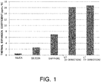
Fig. 1 is a graph of thermal expansion coefficients of various materials in comparison. The thermal expansion of the piezoelectric single crystal is reduced by bonding the material having a small expansion coefficient, and hence the temperature characteristics are improved (e.g. see Non Patent Document 1) . - However, in this method, there is a problem that a stack of a thin piezoelectric single crystal film on a support substrate causes noise referred to as spuriousness or ripples in an antiresonance frequency band. The noise is caused due to reflection from the interface between the piezoelectric single crystal film and the support substrate. As an example,
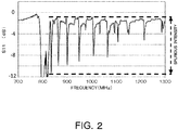
Fig. 2 shows an exemplary spectrum at the reflection coefficient (S11) of a resonator prepared using a composite substrate having a stack of an LT film in 20 µm thickness on a silicon substrate. InFig. 2 , the difference between the peak and bottom of the spectrum is defined as spurious intensity (amplitude). - Some methods are proposed for solving this problem. For example,
Non Patent Document 2 discloses a method in which the bonding surface of LT is roughened with a #1000 grinding wheel to obtain a roughness of 300 nm in the arithmetic average roughness (Ra) and then the LT is bonded to a support substrate through an adhesive. However, in this method, the Lt is bonded to the substrate using an organic adhesive, resulting in a problem of the viewpoint of reliability. Specifically, after bonding, a plurality of processes is scheduled in which the substrate surface is patterned, the substrate is diced, and chips are mounted on devices. However, in the processes, heating processes at temperatures of 250 to 400°C are repeated. As a result, organic substances made up of the adhesive are altered, resulting in a problem that a piezoelectric crystal film on the bonded substrate is peeled or cracked. - Therefore, there is a method in which an intermediate layer made of an inorganic material is formed on a piezoelectric single crystal substrate formed with an irregular structure and a support substrate is joined such that this intermediate layer is sandwiched. Examples of inorganic materials that are used as an intermediate layer include SiOx (1.5 ≤ x ≤ 2.5), Al2O3, AlN, SiN, SiON, and Ta2O5, for example. Representative examples of methods for forming this intermediate layer include chemical vapor deposition (CVD) and physical vapor deposition (PVD) represented by sputtering, for example. Alternatively, a method can also be adopted in which a solution of an organic silicon compound is applied on a wafer and the solution is hardened by heat treatment to form an SiO2 film. After the inorganic material film is deposited by these methods, heat treatment is performed at a high temperature to some extent to eliminate a gas (an out gas) generated from the inside of the film. This is because without performing this process, there is a possibility that gas components generated in a deposited film near the bonding interface in repeating heat treatment in the post-processes of bonding reach the bonding interface to cause a peeling phenomenon from the bonding interface.
- However, piezoelectric single crystals, such as LT and LN, have the upper limit temperature referred to as a Curie temperature at which polarization is destroyed, and can not be heated to higher temperature to maintain the polarization state. In particular, LT has its Curie temperature near 600°C. It is extremely difficult to fully eliminate out gases even if processing is carried out below this temperature, and it is difficult to attain long-term reliability.
- Another reason why high temperature heat treatment is not applicable is that SiO2 that is an inorganic material used for an intermediate layer and a piezoelectric crystal, such as LT and LN, have a great difference in their thermal expansion coefficients. The thermal expansion coefficient of LT and LN is about 16 ppm, and the thermal expansion coefficient of SiO2 is about 0.5 ppm. This difference causes cracks after high temperature treatment, and the subsequent processes can not be performed.
- In the findings by the inventors, after SiO2, Al2O3, AlN, Si3N4, SiON, and Ta2O5 are deposited as intermediate layers each in a thickness of about 2 µm on an LT single crystal substrate for heat treatment, cracks are generated at a temperature of about 500 to 600°C not greatly depending on the materials the intermediate layers or deposition methods. As an example,
Fig. 3 shows results of out gas analysis on samples in which an inorganic layer simulating an intermediate layer were prepared by three different methods. The first one is an analysis result of thermal desorption spectrometry (TDS) in which SiO2 was deposited in a thickness of 5 µm on an LT single crystal substrate by CVD and then heat treatment was applied from at ambient temperature to a temperature of 1,000°C. From this result, the peak of the out gas is at near a temperature of 500°C. However, after that, it is shown that gases are continuously generated until the temperature reaches a temperature of 1,000°C. The second one is a TDS analysis result in which SiO2 was deposited in a thickness of 5 µm by spin coating methyltrimethoxysilane (a solvent was propylene glycol monoethyl ether) and then similar heat treatment was applied. Also in this case, the peak of the out gas is at near a temperature of 500°C, degassing is continued even at a temperature of 600°C or more, and gases are continuously generated even at a temperature of 1,000°C. The third one is a TDS analysis result in which SiO2 was deposited in a thickness of 5 µm by PVD and then similar heat treatment was applied. Also in this case, the peak of the out gas is at near a temperature of 500°C and degassing is continued even at a temperature of 600°C or more and continued until the temperature reaches a temperature of 1,000°C. As described above, it is shown that the intermediate layers deposited by these methods have to be subjected to heat treatment at a temperature of 1,000°C or more for degassing. -
- Non Patent Document 1: "Temperature compensation technology for SAW-Duplexer used in RF front end of smartphone", Dempa Shimbun High Technology, November 8, 2012
- Non Patent Document 2: "A study on Temperature-Compensated Hybrid Substrates for Surface Acoustic Wave Filters", 2010 IEEE International Ultrasonic Symposium (IUS2010), Vol.V1, pp. 637-640, 2010
- The present invention has been made in view of the above circumstances. An object is to provide a composite substrate having a piezoelectric single crystal layer bonded to a support substrate using an inorganic material as an intermediate layer in which peeling hardly occurs even though heating and cooling are repeated in processes after bonding.
-
- (1) A composite substrate according to the present invention has a piezoelectric single crystal substrate, a support substrate, and an intermediate layer provided between the piezoelectric single crystal substrate and the support substrate. The intermediate layer is a film formed of an inorganic material, and at least a part of the film is thermally synthesized silica.
As result of investigation dedicatedly made by the present inventors, the present inventors found that thermally oxidized silica or thermally synthesized silica, such as a synthetic silica sintered body, has the properties that can absorb gasses to some extent. At least a part of the intermediate layer is thermally synthesized silica like the above configuration, and thermally synthesized silica absorbs an out gas possibly generated in heating and cooling in the post-processes even though the rest of the intermediate layer is an inorganic material that insufficiently degases the out gas. Thus, peeling can hardly occur. - (2) In the present invention, the intermediate layer may be separated into at least two layers along a bonding surface of the composite substrate. In this case, a first intermediate layer in contact with the support substrate may be a layer including the thermally synthesized silica.
Since there are a few constraints on a heating temperature, such as the Curie temperature, on the support substrate side, the layer of the intermediate layer in contact with the support substrate can be formed by deposition of thermally synthesized silica. On the other hand, the intermediate layer on the piezoelectric single crystal substrate side is an inorganic material that can be formed by deposition at a low temperature lower as a Curie temperature or less. In repeating heating and cooling in the post-processes, thermally synthesized silica on the support substrate side absorbs an out gas possibly emitted from the intermediate layer on the piezoelectric substrate side, and hence peeling hardly occurs. - (3) In the present invention, a material of the support substrate may be a silicon substrate. In this case, the thermally synthesized silica may be synthesized by thermal oxidation of the silicon substrate. With this configuration, the thermal oxidation layer is formed on the surface of the silicon substrate, and can be used as a part of the intermediate layer. Thermally synthesized silica can be easily formed.
- (4) Alternatively, thermally synthesized silica may be a sintered body of synthetic silica. With this configuration, not only silicon but also a heat resistant substrate such as sapphire, silicon nitride, aluminum nitride, silicon carbide or quartz glass can be used as the material of the support substrate. Silica that is deposited on the support substrate by a given method is heated together with the support substrate, sintered silica is formed on the surface of the support substrate, and the sintered silica can be used as a part of the intermediate layer. A deposition method of silica may be chemical vapor deposition (CVD), physical vapor deposition (PVD), and applying and baking of a solution of an organic silicon compound, for example. For example, in the case of silica prepared by PVD, since the film property immediately after deposition is not dense, sintering may be performed by heat treatment at a temperature of around 1,000°C.
- (5) In the present invention, a material of a second intermediate layer provided on the piezoelectric single crystal substrate side of a first intermediate layer in contact with the support substrate may include at least one of SiOx, Al2O3, AlN, SiN, SiON, and Ta2O5. The above-mentioned substances are preferable because the substances can be deposited and processed by CVD and PVD, for example, at a temperature of 500°C or less that is relatively low temperature.
- (6) In the present invention, the second intermediate layer may have at least two layers having different materials. The at least two layers may be layers of materials having different thermal expansion coefficients. With this configuration, a plurality of layers of different materials can relax thermal stress, and cracks or peeling can hardly occur.
- (7) In the present invention, a thickness of the first intermediate layer may be 20 nm or more. With this configuration, the first intermediate layer can be provided with a sufficient out gas absorption capability.
- (8) In the present invention, a thickness of the second intermediate layer may be 25 µm or less. With this configuration, cracks can be prevented from being generated in the piezoelectric single crystal substrate caused by stress due to the difference in the thermal expansion coefficient between the piezoelectric single crystal substrate and the second intermediate layer. Note that there is no constraint specifically on the lower limit of the thickness of the second intermediate layer. In the case in which the interface to the piezoelectric single crystal substrate is flat, the thickness may be 50 nm or more. In the case in which the interface has an irregular structure, the projections of the piezoelectric single crystal substrate may be accommodated in the second intermediate layer.
- (9) In the present invention, a thermally synthesized silica layer may be further provided on a back surface of the support substrate (i.e., the surface on the opposite side of the surface joined to the piezoelectric single crystal as the intermediate layer is sandwiched). With this configuration, the thermally synthesized silica layer is formed on both sides of the support substrate, the stress applied to the support substrate achieves a balance, and the warpage of the substrate is mitigated.
- (10) In the present invention, the first intermediate layer may be joined to the second intermediate layer as a third intermediate layer formed of amorphous silicon is sandwiched between the first intermediate layer and the second intermediate layer. With this configuration, the joining strength can be improved, and cracks or peeling can hardly occur. The thickness of the third intermediate layer may be 50 nm or less. With this configuration, an out gas generated on the second intermediate layer side can be excellently transmitted on the first intermediate layer side.
- (11) In the present invention, a thickness of the intermediate layer may be 8 µm or less. With this configuration, the heat resistance of the composite substrate can be improved.
- (12) More preferably, the thickness of the intermediate layer may be 7 µm or less. With this configuration, the heat resistance of the composite substrate can be further improved.
- (13) In the present invention, a thickness of the piezoelectric single crystal may be 20 µm or less. With this configuration, with this configuration, the heat resistance of the composite substrate can be improved.
- (14) In the present invention, an interface between the piezoelectric single crystal and the intermediate layer may have an irregular structure. With this configuration, the spurious phenomenon of the resonator prepared from the composite substrate can be suppressed.
- (15) A surface acoustic wave device according to the present invention may be configured including any one of the composite substrates. With this configuration, a small-sized surface acoustic wave device of high performance can be implemented.
- (16) In the present invention, a thickness of the piezoelectric single crystal may be 1.0 times or more and 3.5 times or less of a wavelength a surface acoustic wave. With this configuration, the Q-value of a resonator prepared using the composite substrate can be improved.
- (17) A method for manufacturing a composite substrate according to the present invention includes the steps of: forming a first intermediate layer including thermally synthesized silica on a surface of a support substrate; forming a second intermediate layer including an inorganic material on a surface of a piezoelectric single crystal substrate; flattening a surface of the second intermediate layer; and bonding a surface of the first intermediate layer to the flattened surface of the second intermediate layer.
The first intermediate layer that is a part of the intermediate layer includes thermally synthesized silica by the manufacturing method, the first intermediate layer can absorb an out gas possibly generated from the second intermediate layer in heating and cooling in the post-processes. Thus, peeling can hardly occur in the bonded substrates. - (18) In the present invention, the step of flattening the surface of the first intermediate layer may be further included. With this configuration, even in the case in which the surface of the first intermediate layer obtained by forming thermally synthesized silica is not flat, firm bonding can be implemented. Note that the step of flattening the surface of the first intermediate layer is performed prior to the step of bonding.
- (19) In the present invention, the step of forming irregularities on the surface of the piezoelectric single crystal substrate may be further included. With this configuration, the properties of a device prepared from the composite substrate obtained by the manufacturing method can be made excellent. Specifically, for example, the spurious phenomenon of the resonator prepared from the composite substrate obtained by the manufacturing method can be suppressed.
- (20) In the present invention, the first intermediate layer may be thermally synthesized silica in which a silica layer deposited by chemical vapor deposition (CVD) is sintered at a temperature of 800°C or more.
- (21) The first intermediate layer may be thermally synthesized silica in which a silica layer deposited by physical vapor deposition (PVD) is sintered at a temperature of 800°C or more.
- (22) Alternatively, the first intermediate layer may be a layer of thermally synthesized silica in which a solution of an organic silicon compound is applied and sintered at a temperature of 800°C or more.
In the methods of (20) to (22), the silica layer is sintered at a temperature of 800°C or more. Thus, the degassing of the silica layer is promoted, and a sintered, fine thermally synthesized silica (sintered silica) film can be formed. The thermally synthesized silica has excellent absorption capability. Note that the temperature in sintering may be preferably a temperature of 1,000°C or more. - (23) In the present invention, a material of the support substrate may be selected from silicon, sapphire, silicon carbide, silicon nitride, aluminum nitride, and silica glass. With the use of the support substrate having a material of excellent heat resistance, the silica layer can be sintered at a high temperature of 800°C or more in the methods of (20) to (22).
- (24) In the case in which the material of the support substrate is silicon, the first intermediate layer may be formed by thermal oxidation of the support substrate. With this configuration, the thermal oxidation layer is formed on the surface of the silicon substrate, and can be used as a part of the intermediate layer. In addition, thermally synthesized silica can be easily formed.
- (25) In the present invention, the step of heating the second intermediate layer at a highest temperature lower than a Curie temperature of the piezoelectric single crystal may be further included. When the second intermediate layer is heated at a low temperature as described above, residual gases can be reduced, an out gas generated by repeating heating and cooling in the post-processes can be suppressed, and the occurrence of peeling can be reduced.
- (26) A temperature when the second intermediate layer is heated may be preferably a temperature of 600°C or less. With this configuration, cracking of the second intermediate layer due to the difference between the thermal expansions can be suppressed.
- (27) In the present invention, in addition to the surface of the support substrate, a thermally synthesized silica layer having a material the same as a material of the first intermediate layer may also be formed on a back surface of the support substrate (i.e., the surface on the opposite side of the surface joined to the piezoelectric single crystal as the intermediate layer is sandwiched). With this configuration, the thermally synthesized silica layer is formed on both sides of the support substrate, stress applied to the support substrate achieves a balance, and hence the warpage of the substrate can be mitigated. Note that after the support substrate is bonded to the piezoelectric single crystal substrate, the thermally synthesized silica layer on the back surface of the support substrate may be appropriately removed using hydrofluoric acid, for example.
- (28) In the present invention, an amorphous silicon layer may be further deposited on at least one of the surface of the first intermediate layer and the surface of the second intermediate layer, and then the first intermediate layer may be bonded to the second intermediate layer. With this configuration, the joining strength can be improved, and cracks or peeling can hardly occur.
- (29) At this time, a total thickness of the amorphous silicon layer may be 50 nm or less. With this configuration, an out gas generated on the second intermediate layer side can be excellently transmitted on the first intermediate layer side.
- (30) In the present invention, an activation process may be applied to at least one surface of the first intermediate layer and the second intermediate layer, and then the surface of the first intermediate layer may be bonded to the surface of the second intermediate layer.
- (31) The surface activation process may be any one of ozone water treatment, UV ozone treatment, ion beam treatment, and plasma treatment. By the surface activation process, firm bonding can be implemented.
- (32) In the present invention, the surface of the first intermediate layer and/or the surface of the second intermediate layer may be flattened by chemical-mechanical polishing.
- (33) In the present invention, a material of the second intermediate layer may include any one of SiOx, Al2O3, AlN, SiN, SiON, and Ta2O5. The above-mentioned substances are preferable because the substances can be deposited and processed by CVD and PVD, for example, at a temperature of 500°C or less that is relatively low temperature.
- (34) In the present invention, the second intermediate layer may be formed by chemical vapor deposition (CVD).
- (35) Alternatively, the second intermediate layer may be formed by physical vapor deposition (PVD).
- (36) Alternatively, the second intermediate layer may be formed in which a solution of an organic silicon compound is applied and the applied organic silicon compound is hardened.
- (37) In the present invention, the step of performing a process of ion implantation into the piezoelectric single crystal substrate is included prior to the step of bonding, and peeling may be performed at an interface in a region in which the ion is implanted after the step of bonding.
- (38) In the step of performing the ion implantation process, a hydrogen ion may be implanted in an amount of 6.0 × 10¹⁶ atoms/cm2 to 2.75 × 10¹⁷ atoms/cm2.
- (39) Alternatively, in the step of performing the ion implantation process, a hydrogen molecule ion may be implanted in an amount of 3.0 × 10¹⁶ atoms/cm2 to 1.37 × 10¹⁷ atoms/cm2.
- (40) In the step of peeling, mechanical peeling may be performed along a region in which the ion is implanted.
- (41) Alternatively, in the step of peeling, peeling may be performed using a flash lamp annealing.
- (42) In the present invention, the step of grinding and/or polishing the piezoelectric single crystal substrate to reduce a thickness may be included after the step of bonding.
-
-
Fig. 1 is a graph of thermal expansion coefficients of various materials in comparison. -
Fig. 2 shows a spectrum of the reflection coefficient of a resonator prepared from a conventional composite substrate. -
Fig. 3 shows the temperature dependence of amounts of out gas emission from intermediate layers. -
Fig. 4 shows a processing method of a support substrate before bonding. -
Fig. 5 shows a processing method of a piezoelectric single crystal substrate before bonding. -
Fig. 6 shows a bonding method and a processing method after bonding. -
Fig. 7 schematically shows the structure of a composite substrate provided with an amorphous silicon layer between a first intermediate layer and a second intermediate layer. -
Fig. 8 shows the cross section of a microphotograph of a composite substrate prepared in Example 1. -
Fig. 9 shows a spectrum of the reflection coefficient of a resonator prepared in Example 8. - A
composite substrate 1 according an embodiment is manufactured through processes in which asupport substrate 100 and a piezoelectricsingle crystal substrate 200 are processed before bonding and then these two substrates are bonded to each other. In the following, manufacturing methods will be described with reference toFigs. 4 to 6 . - First, the
support substrate 100 is prepared (Fig. 4(a) ). Thesupport substrate 100 is selected from silicon, sapphire, silicon carbide, silicon nitride, aluminum nitride, and silica glass. - Subsequently, a first
intermediate layer 310 including thermally synthesized silica is formed on the surface of the support substrate 100 (Fig. 4(b) ). At this time, a thermally synthesized silica layer having the same material as the firstintermediate layer 310 may be formed on the back surface of thesupport substrate 100. Note that after thesupport substrate 100 is bonded to the piezoelectricsingle crystal substrate 200, the silica layer on the back surface may be appropriately removed using hydrofluoric acid, for example. In the case in which the material of thesupport substrate 100 is silicon, a thermally oxidized silica film to be the firstintermediate layer 310 can be formed by thermal oxidation of a silicon substrate. Since thermally oxidized silica is grown at high temperature, the thermally oxidized silica has the properties of being fine with few impurities and can absorb gases to some extent. - The first
intermediate layer 310 can be formed by methods below regardless of whether the material of thesupport substrate 100 is silicon or not. That is, the firstintermediate layer 310 may be formed by sintering a silica layer deposited by chemical vapor deposition (CVD) at a temperature of 800°C or more. The firstintermediate layer 310 may be formed by sintering a silica layer deposited by physical vapor deposition (PVD) at a temperature of 800°C or more. Alternatively, the firstintermediate layer 310 may be formed in which a solution of an organic silicon compound is applied and then sintered at a temperature of 800°C or more. In the case in which the firstintermediate layer 310 is formed in a silica sintered body, a heat resistant substrate is preferably used such that synthetic silica deposited on thesupport substrate 100 can be sintered together with thesupport substrate 100. - Subsequently, the surface of the first
intermediate layer 310 is flattened as necessary (Fig. 4(c) ). This flattening may be performed by chemical-mechanical polishing. Note that in the case in which a silicon substrate having a mirror-finished surface is used as thesupport substrate 100 and the firstintermediate layer 310 is formed by thermal oxidation, the surface of the firstintermediate layer 310 has a mirror surface similar to the base, and hence this flattening process is unnecessary. - Although not shown in the drawings, processes below may be performed as necessary in order to improve joining strength in bonding. For example, amorphous silicon may be deposited on the surface of the first
intermediate layer 310. Stacking amorphous silicon makes the bonding interface that is Si/SiO2 or Si/Si, and this provides joining strength slightly higher than SiO2/SiO2 bonding (see detail, Tong Q.Y. and Gosele U., Semiconductor Wafer Bonding, Science and Technology, Chapter 4.7.1, 1999). The thickness of the amorphous silicon to be deposited is preferably 50 nm or less such that gas transmission is not inhibited. The surface of the firstintermediate layer 310 may be subjected to activation. The surface activation process may be any one of ozone water treatment, UV ozone treatment, ion beam treatment, and plasma treatment, for example. - With the processes above, the processes before bonding for the
support substrate 100 is finished. - First, the piezoelectric
single crystal substrate 200 is prepared (Fig. 5 (a) ). The piezoelectricsingle crystal substrate 200 is a piezoelectric single crystal, such as lithium tantalate (LT) and lithium niobate (LN). Subsequently, irregularities are formed on the surface of the piezoelectricsingle crystal substrate 200 as necessary (Fig. 5 (b) ). The irregularities have the effect that suppresses the spurious phenomenon of a resonator prepared from thecomposite substrate 1. In the case in which thecomposite substrate 1 is used for the application that spuriousness causes no problem, this process may be omitted. - Subsequently, a second
intermediate layer 320 is formed by depositing the secondintermediate layer 320 including an inorganic material on the surface of the piezoelectric single crystal substrate 200 (Fig. 5 (c) ). The material of the secondintermediate layer 320 includes any one of SiOx (e.g. SiO2), Al2O3, AlN, SiN, SiON, and Ta2O5. The secondintermediate layer 320 can be formed by methods below. That is, the secondintermediate layer 320 may be deposited by chemical vapor deposition (CVD). The second intermediate layer may be deposited by physical vapor deposition (PVD). Alternatively, the secondintermediate layer 320 may be deposited in which a solution of an organic silicon compound is applied and then hardened. In order to reduce residual gases, the secondintermediate layer 320 formed by any one of the methods may be heated at a temperature lower than the Curie temperature of the piezoelectric crystal. In order to prevent the secondintermediate layer 320 from cracking due to the difference in the thermal expansion coefficient between the piezoelectricsingle crystal substrate 200 and the secondintermediate layer 320, a heating temperature is preferably at a temperature of 600°C or less. The secondintermediate layer 320 may be configured in which thelayer 320 has at least two layers having different materials. - Subsequently, the surface of the formed second
intermediate layer 320 is flattened (Fig. 5 (d) ). This flattening may be performed by chemical-mechanical polishing. - Although not shown in the drawings, processes below may be performed as necessary in order to improve joining strength in bonding. For example, amorphous silicon may be deposited on the surface of the second
intermediate layer 320. The thickness of the amorphous silicon to be deposited is preferably 50 nm or less such that gas transmission is not inhibited. Note that in the case in which amorphous silicon is also deposited on the firstintermediate layer 310, the total thickness may be 50 nm or less. The surface of the secondintermediate layer 320 may be subjected to activation. The surface activation process may be any one of ozone water treatment, UV ozone treatment, ion beam treatment, and plasma treatment, for example. - With the processes above, the processes for the piezoelectric
single crystal substrate 200 before bonding are finished. - On the
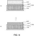
support substrate 100 and the piezoelectricsingle crystal substrate 200 processed as described above, the surface of the firstintermediate layer 310 is bonded to the surface of the second intermediate layer 320 (Fig. 6 (a) ). At this time, joining strength may be improved by heating the bonded substrates at a low temperature (e.g., 120°C). - Subsequently, the piezoelectric
single crystal substrate 200 is ground and polished to reduce the thickness. For example, the thickness of the piezoelectricsingle crystal substrate 200 is reduced to a thickness of about 20 µm (Fig. 6 (b) ). After that, additional heat treatment is performed further as necessary, and joining force may be reinforced. The firstintermediate layer 310 and the secondintermediate layer 320 thus bonded and joined configure anintermediate layer 300. As shown inFig. 7 , in the configuration of thecomposite substrate 1 provided with an amorphous silicon layer (a third intermediate layer) 330 between the firstintermediate layer 310 and the secondintermediate layer 320, the firstintermediate layer 310, the secondintermediate layer 320, and the thirdintermediate layer 330 configure theintermediate layer 300. - By the manufacturing method described above, the
composite substrate 1 having the piezoelectricsingle crystal substrate 200 joined to thesupport substrate 100 with theintermediate layer 300 sandwiched can be manufactured. - On the surface of the piezoelectric
single crystal substrate 200 of the preparedcomposite substrate 1, an aluminum (Al) thin film in a thickness of 0.4 µm was sputtered, electrodes were formed by photolithography, and then a four-stage rudder filter formed of a two-stage parallel resonators and a four-stage series resonator at a wavelength of 5 µm and a resonator were prepared. For photolithographic exposure, a g-line stepper was used, and for Al etching, a mixed gas of Cl2, BCl3, N2, and CF4 was used. With the use of a network analyzer, the reflection coefficient (S11) of the prepared four-stage rudder filter was measured. The difference between the peak and bottom of observed spuriousness was evaluated as spurious intensity. - The relationship between the Q-value and the resonance frequency of the prepared resonator was found by Equation (1) below.
[Equation 1]
Here, ω is the angular frequency, and τ is the group delay time. The Q-value is the value indicating the sharpness of the waveform of resonance, and a filter having a higher Q value can be of excellent properties with a small loss. Since the Q-value has frequency dependency, the maximum value (Qmax) of the Q-value was evaluated. - An LT substrate in a diameter of six inches having a roughness of about 230 nm (in P-V, about 1.7 µm) at Ra (arithmetic average roughness) was prepared as a piezoelectric single crystal substrate. On the LT substrate, an SiO2 film was formed by deposition in a thickness of about 10 µm by plasma CVD using silane and oxygen gas as raw material gases. This SiO2 film was subjected to heat treatment at a temperature of about 400°C, the surface was polished and mirror-finished, and the SiO2 film was finished in a film thickness of about 2 µm.
- An Si substrate in a diameter of six inches having a thermal oxidation film grown in a thickness of 500 nm was prepared as a support substrate. After that, plasma surface activation was applied to both of the LT substrate deposited with the SiO2 film and the Si substrate having the thermal oxidation film grown. The two substrates were bonded to each other and subjected to heat treatment at a temperature of 120°C, and then the LT was ground and polished to reduce the thickness to about 20 µm. The cross section of a microphotograph of the composite substrate thus finished is shown in
Fig. 8 . - A heat resistance test was examined in which the wafer of the composite substrate was diced in two-millimeter squares and reciprocated between a hot plate at a temperature of 200°C and a metal cooling stage (the substrate was held for 30 seconds each on the hot plate and on the cooling stage). The wafer was reciprocated for 100 times. However, peeling, for example, was not observed.
- Note that the similar experiment was performed in which an oxide film was formed on the surface of a mirror-finished LT substrate under the same conditions. However, the entirely similar result was obtained regarding heat resistance. In the case of applications in which spuriousness causes no problem, an oxide film was formed on the mirror-finished LT substrate for performing the similar methods, and hence this shown that the present invention is applicable as it is.
- An experiment similar to Example 1 was performed using an LT substrate provided with an SiO2 film similarly to Example 1 and an Si substrate without thermal oxidation. As a result of a heat resistance test similar to Example 1, peeling was observed at edges in the fifth reciprocation. With the comparison between Example 1 and Comparative Example 1, the LT substrate provided with the SiO2 film by plasma CVD was bonded to the Si substrate having the thermal oxidation film grown, and hence it was shown that peeling can be suppressed compared with the case in which the Si substrate with no thermal oxidation film grown is bonded.
- An LT substrate in a diameter of six inches having a roughness of about 230 nm (in P-V, about 1.7 µm) in Ra was prepared. On the LT substrate, a process was repeated for a plurality of times in which a solution of an organic silicon compound was spin-coated and heated at a temperature of 350°C, and hence an SiO2 layer in a thickness of about 5 µm was obtained. The solution of the organic silicon compound used here is two types of perhydropolysilazane (a solvent was dibutylether) and methyltrimethoxysilane (a solvent was propylene glycol monoethyl ether).
- After heat treatment at a temperature of about 400°C, the surface of this SiO2 film was polished and mirror-finished. An Si substrate in a diameter of six inches having a thermal oxidation film grown in a thickness of 500 nm was prepared. Plasma surface activation was applied to the two substrates. The two substrates were bonded to each other and subjected to heat treatment at a temperature of 120°C, the LT was ground and polished to reduce the thickness to 20 µm, and then a composite substrate was obtained.
- A heat resistance test was examined in which the wafer of the composite substrate was diced in two-millimeter squares and reciprocated between a hot plate at a temperature of 200°C and a metal cooling stage (the substrate was held for 30 seconds each on the hot plate and on the cooling stage). The wafer was reciprocated for 100 times. However, peeling, for example, was not observed.
- An experiment similar to Example 2 was performed using an LT substrate provided with an SiO2 film similarly to Example 2 and an Si substrate without thermal oxidation. As a result of a heat resistance test similar to Example 2, peeling was observed at edges in the seventh reciprocation. With the comparison between Example 2 and Comparative Example 2, the LT substrate provided with the SiO2 film by spin-coating and heating the solution of the organic silicon compound was bonded to the Si substrate having the thermal oxidation film grown, and hence it was shown that peeling can be suppressed compared with the case in which the Si substrate with no thermal oxidation film grown is bonded.
- An LT substrate in a diameter of six inches having a roughness of about 230 nm (in P-V, about 1.7 µm) in Ra was prepared. On the LT substrate, an SiO2 film was deposited in a thickness of about 10 µm by PVD (here, magnetron sputtering). After heat treatment at a temperature of about 400°C, the surface of this SiO2 film was polished and mirror-finished. An Si substrate in a diameter of six inches having a thermal oxidation film grown in a thickness of 500 nm was prepared. Plasma surface activation was applied to the two substrates. The two substrates were bonded to each other and subjected to heat treatment at a temperature of 120°C, the LT was ground and polished to reduce the thickness to 20 µm, and then a composite substrate was obtained.
- A heat resistance test was examined in which the wafer of the composite substrate was diced in two-millimeter squares and reciprocated between a hot plate at a temperature of 200°C and a metal cooling stage (the substrate was held for 30 seconds each on the hot plate and on the cooling stage). The wafer was reciprocated for 100 times. However, peeling, for example, was not observed.
- An experiment similar to Example 3 was performed using an LT substrate provided with an SiO2 film similarly to Example 3 and an Si substrate without thermal oxidation. As a result of a heat resistance test similar to Example 3, peeling was observed at edges in the second reciprocation. With the comparison between Example 3 and Comparative Example 3, the LT substrate provided with the SiO2 film by PVD was bonded to the Si substrate having the thermal oxidation film grown, and hence it was shown that peeling can be suppressed compared with the case in which the Si substrate with no thermal oxidation film grown is bonded.
- A plurality of LT substrates in a diameter of six inches having a roughness of about 230 nm (in P-V, about 1.7 µm) in Ra was prepared. On the prepared LT substrates, an SiO2 film was deposited in a thickness of about 10 µm by plasma CVD. Heat treatment at a temperature of about 400°C was applied to the SiO2 film, the surface was polished and mirror-finished, and then amorphous silicon (a-Si) was deposited in various thicknesses as shown in Table 1. The amorphous silicon was deposited by varying thicknesses by PVD (magnetron sputtering) and by CVD. Plasma surface activation was applied to both of the LT substrate and the Si substrate in a diameter of six inches having the thermal oxidation film grown in a thickness of 500 nm. The two substrates were bonded to each other and subjected to heat treatment at a temperature of 120°C, the LT was ground and polished to reduce the thickness to 20 µm, and then a composite substrate was obtained.
- A heat resistance test was examined in which the wafer of the obtained composite substrate was diced in two-millimeter squares and reciprocated between a hot plate at a temperature of 200°C and a metal cooling stage (the substrate was held for 30 seconds each on the hot plate and on the cooling stage). The result is shown in Table 1. It is shown that after the thickness of the amorphous silicon exceeds 50 nm both by PVD and by CVD, the resistance is rapidly degraded. It is considered that gases generated from SiO2 on the LT side fail to transmit the amorphous silicon film due to an increase in the thickness of the amorphous silicon and the absorption of the gasses to the Si thermal oxidation film is inhibited.
[Table 1] a-Si Thickness (nm) 3 5 10 20 35 50 65 80 80 100 PVD > 100Times > 100Times > 100Times > 100Times > 100Times > 100Times 75Times 52Times 12Times 3Times CVD > 100Times > 100Times > 100Times > 100Times > 100Times > 100Times 19Times 11Times 5Times 2Times - Amorphous silicon was deposited on the side of an Si substrate having a thermal oxidation film grown, not on the LT substrate side, and an experiment similar to Example 4 was performed. The result was almost the same as the result in Example 4. From the result, it was shown that amorphous silicon can be provided on any of the LT substrate side and the Si substrate side.
- Amorphous silicon was deposited on both of an LT substrate and an oxidation Si substrate side, and an experiment similar to Example 4 was performed. The thickness of the amorphous silicon was the total thickness of the amorphous silicon films deposited on both substrates. The result was almost the same as the result in Example 4. From the result, it was shown that amorphous silicon can be provided on both of the LT substrate side and the Si substrate side.
- The experiment was performed as the surface activation method was changed to ozone water treatment, UV ozone treatment, and ion beam treatment. However, no difference was found in the results of bonding. It is thought that the present invention does not strongly depend on activation methods. No great difference was observed when surface activation was applied to only one substrate.
- A four-stage rudder filter was formed on a composite substrate prepared by the method in Example 1, the spectrum of the reflection coefficient (S11) was measured, and the spurious properties were evaluated. As a result, as shown in
Fig. 9 , it was confirmed that spurious strength is 1 dB or less. It was revealed that the resonator prepared by this method can effectively reduce spuriousness. - An experiment similar to Example 1 was performed by changing the thickness of a thermal oxidation film grown on an Si substrate. As a result, an effect was confirmed in the thermal oxidation films in a thickness of 20 nm or more. However, in thermal oxidation films in a thickness of less than 20 nm, out gas absorption capability was insufficient, and peeling was sometimes observed in heating and cooling cycle tests.
- An experiment similar to Example 1 was performed by changing the thickness of an SiO2 film deposited on an LT substrate. The result is shown in Table 2. The thickness of the deposited SiO2 shown in Table 2 is the thickness after the surface was flattened. This result revealed that when the thickness of the SiO2 film (only the deposited film, the thermal oxidation film is not included) exceeds 25 µm, cracks were generated in the LT layer. It is thought that the cracks were generated by stress due to the difference in the expansion coefficient between LT and SiO2. In the case in which the thickness of SiO2 is 25 µm or less, SiO2 can be deformed following the difference in the expansion coefficient to some extent. However, it is thought that when the thickness is 25 µm or more, cracks are generated due to stress relaxation.
[Table 2] Thickness of deposited SiO2 (µ m) 1 2 5 10 20 25 30 Crack generation state No crack No crack No crack No crack No crack Some cracks on edges Cracks observed on whole wafer - An LT substrate in a diameter of six inches having a mirror-finished surface on one side was prepared. On the mirror surface side of the LT substrate, an Al2O3 film was deposited in a thickness of 1 µm by sputtering. On the Al2O3 film of the Al2O3 film attached LT substrate, an SiO2 film was deposited in a thickness of about 10 µm by plasma CVD using silane and oxygen gas as raw material gases. The film stack of Al2O3 and SiO2 was subjected to heat treatment at a temperature of about 400°C, the surface was polished and mirror-finished, and the SiO2 film was finished in a film thickness of about 2 µm.
- An Si substrate in a diameter of six inches having a thermal oxidation film grown in a thickness of 500 nm was prepared. Plasma surface activation was applied to the two substrates. The two substrates were bonded to each other and subjected to heat treatment at a temperature of 120°C, the LT was ground and polished to reduce the thickness to about 6 µm, and then a composite substrate was obtained.
- A heat resistance test was examined in which the wafer of the composite substrate was diced in two-millimeter squares and reciprocated between a hot plate at a temperature of 200°C and a metal cooling stage (the substrate was held for 30 seconds each on the hot plate and on the cooling stage). The wafer was reciprocated up to 200 reciprocations. However, peeling, for example, was not observed. From the example, it was shown that a multilayered intermediate layer (i.e., the second intermediate layer) may be provided on the LT substrate side before bonding.
- An LT substrate in a diameter of six inches having a roughness of about 230 nm (in P-V, about 1.7 µm) at Ra (arithmetic average roughness) was prepared. On the LT substrate, an SiO2 film was formed by deposition in a thickness of about 10 µm by plasma CVD using silane and oxygen gas as raw material gases. This SiO2 film was subjected to heat treatment at a temperature of about 400°C, the surface was polished and mirror-finished, and the SiO2 film was finished in a film thickness of about 2 µm.
- A sapphire substrate in a diameter of six inches was prepared, and on the substrate, an SiO2 film was deposited in a thickness of about 5 µm by plasma CVD. The SiO2 film on the sapphire substrate was sintered by heat treatment at a temperature of 800°C, the surface was polished and mirror-finished, and the SiO2 film was finished in a film thickness of 1 µm.
- A plasma activation process was applied to both of the SiO2 film deposited on the LT substrate and the sintered SiO2 film deposited on the sapphire substrate, the two substrates were bonded to each other and subjected to heat treatment at a temperature of 120°C, the LT was ground and polished to reduce the thickness to 20 µm, and then a composite substrate was obtained.
- A heat resistance test was examined in which the wafer of the composite substrate was diced in two-millimeter squares and reciprocated between a hot plate at a temperature of 200°C and a metal cooling stage (the substrate was held for 30 seconds each on the hot plate and on the cooling stage). The wafer was reciprocated for 100 times. However, peeling, for example, was not observed. From the example, it was shown that a sapphire substrate can be used as a support substrate. It was shown that thermally synthesized silica obtained by heating and sintering SiO2 deposited by CVD can be used for an intermediate layer (i.e., the first intermediate layer) provided on the support substrate side before bonding.
- An LT substrate in a diameter of six inches having a roughness of about 230 nm (in P-V, about 1.7 µm) at Ra (arithmetic average roughness) was prepared. On the LT substrate, an SiO2 film was formed by deposition in a thickness of about 10 µm by plasma CVD using silane and oxygen gas as raw material gases. This SiO2 film was subjected to heat treatment at a temperature of about 400°C, the surface was polished and mirror-finished, and the SiO2 film was finished in a film thickness of about 2 µm.
- A sapphire substrate in a diameter of six inches was prepared, and on the substrate, an SiO2 film was deposited in a thickness of about 10 µm by PVD (magnetron sputtering). The SiO2 film on the sapphire substrate was sintered by heat treatment at a temperature of 900°C, the surface was polished and mirror-finished, and SiO2 film was finished in a film thickness of 1 µm.
- A plasma activation process was applied to both of the SiO2 film deposited on the LT substrate and the sintered SiO2 film deposited on the sapphire substrate, the two substrates were bonded to each other and subjected to heat treatment at a temperature of 120°C, the LT was ground and polished to reduce the thickness to 20 µm, and then a composite substrate was obtained.
- A heat resistance test was examined in which the wafer of the composite substrate was diced in two-millimeter squares and reciprocated between a hot plate at a temperature of 200°C and a metal cooling stage (the substrate was held for 30 seconds each on the hot plate and on the cooling stage). The wafer was reciprocated for 100 times. However, peeling, for example, was not observed. From the example, it was shown that a sapphire substrate can be used as a support substrate. It was shown that thermally synthesized silica obtained by heating and sintering SiO2 deposited by PVD can be used for an intermediate layer (i.e., the first intermediate layer) provided on the support substrate side before bonding.
- An LT substrate in a diameter of six inches having a roughness of about 230 nm (in P-V, about 1.7 µm) at Ra (arithmetic average roughness) was prepared. On the LT substrate, an SiO2 film was formed by deposition in a thickness of about 10 µm by plasma CVD using silane and oxygen gas as raw material gases. This SiO2 film was subjected to heat treatment at a temperature of about 400°C, the surface was polished and mirror-finished, and the SiO2 film was finished in a film thickness of about 2 µm.
- A sapphire substrate in a diameter of six inches was prepared, and on the substrate, an SiO2 film was deposited in a thickness of about 3 µm by repeating a process of spin coating a solution of the organic silicon compound (a dibutylether solution of perhydropolysilazane) and a process of thermosetting at a temperature of 350°C for a few times. The SiO2 film on the sapphire substrate was sintered by heat treatment at a temperature of 900°C, the surface was polished and mirror-finished, and the thickness of the SiO2 film was finished to a film thickness of 0.5 µm.
- A plasma activation process was applied to both of the SiO2 film deposited on the LT substrate and the sintered SiO2 film deposited on the sapphire substrate, the two substrates were bonded to each other and subjected to heat treatment at a temperature of 120°C, the LT was ground and polished to reduce the thickness to 20 µm, and then a composite substrate was obtained.
- A heat resistance test was examined in which the wafer of the composite substrate was diced in two-millimeter squares and reciprocated between a hot plate at a temperature of 200°C and a metal cooling stage (the substrate was held for 30 seconds each on the hot plate and on the cooling stage). The wafer was reciprocated for 100 times. However, peeling, for example, was not observed. From the example, it was shown that a sapphire substrate can be used as a support substrate. It was shown that thermally synthesized silica obtained by applying, heating, and sintering organic silicon can be used for an intermediate layer (i.e., the first intermediate layer) provided on the support substrate side before bonding.
- An LT substrate in a diameter of six inches having a roughness of about 230 nm (in P-V, about 1.7 µm) at Ra (arithmetic average roughness) was prepared. On the LT substrate, an SiO2 film was formed by deposition in a thickness of about 10 µm by plasma CVD using silane and oxygen gas as raw material gases. This SiO2 film was subjected to heat treatment at a temperature of about 400°C, the surface was polished and mirror-finished, and the SiO2 film was finished in a film thickness of about 2 µm.
- A silica glass substrate in a diameter of six inches was prepared, and on the substrate, an SiO2 film was deposited in a thickness of about 3 µm by repeating a process of spin coating a solution of the organic silicon compound (a propylene glycol monoethyl ether solution of methyltrimethoxysilane) and a process of thermosetting at a temperature of 350°C for a few times. The SiO2 film on the silica glass substrate was sintered by heat treatment at a temperature of 1,000°C, the surface was polished and mirror-finished, and the thickness of the SiO2 film was finished to a film thickness of 0.5 µm.
- A plasma activation process was applied to both of the SiO2 film deposited on the LT substrate and the sintered SiO2 film deposited on the silica glass substrate, the two substrates were bonded to each other and subjected to heat treatment at a temperature of 120°C, the LT was ground and polished to reduce the thickness to 20 µm, and then a composite substrate was obtained.
- A heat resistance test was examined in which the wafer of the composite substrate was diced in two-millimeter squares and reciprocated between a hot plate at a temperature of 200°C and a metal cooling stage (the substrate was held for 30 seconds each on the hot plate and on the cooling stage). The wafer was reciprocated for 100 times. However, peeling, for example, was not observed. From the example, it was shown that a silica glass substrate can be used as a support substrate. It was shown that thermally synthesized silica obtained by applying, heating, and sintering organic silicon can be used for an intermediate layer (i.e., the first intermediate layer) provided on the support substrate side before bonding.
- A plurality of LT substrates in irregular structures having similar Ra (arithmetic average roughness) and RSm (The Mean width of profile elements (roughness) was prepared (Ra = 300 nm ±10%, RSm = 3 µm ±10%, and Rz = 2.0 µm ±10%). Here, the irregular structure of the LT substrate was formed by polishing using free abrasive grains. Here, the definitions of Ra and RSm were in compliance with JIS B 0601:2001 and ISO 4287:1997, and calculated from the profiles measured using an atomic force microscope (AFM).
- Subsequently, on the surface having the irregular structure of the LT substrate, SiO2 was deposited in a thickness of about 10 µm at a temperature of 35°C using plasma CVD, the surface having SiO2 deposited was polished to form a mirror surface. At this time, the polishing amount was changed depending on the LT substrates, and the thickness of SiO2 was from 1.5 µm to 9.5 µm.
- An Si substrate to be a support substrate was subjected to heat treatment at a temperature of 850°C in an oxygen atmosphere, and hence thermally oxidized silica in a thickness of 0.5 µm was formed on the surface of the Si substrate.
- Thermally oxidized silica formed on both of the SiO2 mirror surface and the surface of the Si substrate was subjected to plasma surface activation, the LT substrate was bonded to the support substrate, the LT substrate was polished, and then a composite substrate was prepared. At this time, the polishing amount was changed depending on the substrates, and the thickness of the LT substrate was 5 µm to 25 µm.
- The composite substrate wafers were loaded into an oven and gradually heated, and a temperature at which the LT substrate starts peeling was measured. Electrodes were formed on the surfaces of the composite substrates, and the evaluation of the surface acoustic wave properties was performed. The evaluation results are shown in Tables 3 and 4.
[Table 3] Intermediate layer thickness [µ m] LT thickness [µ m] Peeling starting temperature [°C] Intermediate layer thickness /wavelength LT thickness /wavelength S11 spurious intensity [dB] Qmax Si substrate side LT substrate side Total 0.5 1.5 2.0 5.0 350 0.4 1.0 0.20 4000 0.5 1.5 2.0 7.5 340 0. 4 1.5 0.20 4000 0.5 1.5 2.0 10.0 320 0.4 2.0 0.10 4000 0.5 1.5 2.0 12.5 310 0. 4 2.5 0. 40 4000 0.5 1.5 2.0 15.0 300 0.4 3.0 0.40 4000 0.5 1.5 2.0 17.5 290 0.4 3.5 0.55 3250 0.5 1.5 2.0 20.0 280 0. 4 4.0 0.70 2500 0.5 1.5 2.0 22.5 250 0.4 4. 5 0.65 2150 0.5 1.5 2.0 25.0 220 0.4 5.0 0.60 1800 0.5 2.5 3.0 5.0 330 0.6 1.0 0.30 3500 0.5 2.5 3.0 7.5 335 0.6 1.5 0.35 4000 0.5 2.5 3.0 10.0 310 0.5 2.0 0.30 4000 0.5 2.5 3.0 12.5 303 0.6 2.5 0.28 4000 0.5 2.5 3.0 15.0 295 0. 6 3.0 0.25 4000 0.5 2.5 3.0 17.5 283 0. 6 3.5 0.35 3250 0.5 2.5 3.0 20.0 270 0.6 4.0 0.45 2500 0.5 2.5 3.0 22.5 235 0.6 4.5 0.63 2150 0.5 2.5 3.0 25.0 200 0. 6 5.0 0.80 1800 0.5 3.5 4.0 5.0 320 0.8 1.0 0.40 3200 0.5 3.5 4.0 7.5 330 0.8 1.5 0.30 3800 0.5 3.5 4.0 10.0 300 0.8 2.0 0.20 4000 0.5 3.5 4.0 12.5 295 0.8 2.5 0.20 3900 0.5 3.5 4.0 15.0 290 0.8 3.0 0.20 3800 0.5 3.5 4.0 17.5 275 0.8 3.5 0.38 3150 0.5 3.5 4.0 20.0 260 0.8 4.0 0.55 2500 0.5 3.5 4.0 22.5 220 0.8 4.5 0.43 2150 0.5 3.5 4.0 25.0 180 0.8 5.0 0.30 1800 0.5 4.5 5.0 5.0 300 1.0 1.0 0.20 3000 0.5 4.5 5.0 7.5 320 1.0 1. 5 0.20 3800 0.5 4.5 5.0 10.0 290 1.0 2.0 0.50 4000 0.5 4.5 5.0 12.5 288 1.0 2.5 0.48 3900 0.5 4.5 5.0 15.0 285 1.0 3.0 0.45 3800 0.5 4.5 5.0 17.5 270 1.0 3.5 0.38 3150 0.5 4.5 5.0 20.0 255 1.0 4.0 0.30 2500 0.5 4.5 5.0 22.5 213 1.0 4.5 0.50 2150 0.5 4.5 5.0 25.0 170 1.0 5.0 0.70 1800 0.5 5.5 6.0 5.0 280 1. 2 1.0 0.30 2800 0.5 5.5 6.0 7.5 300 1.2 1.5 0.40 3700 0.5 5.5 6.0 10.0 280 1.2 2.0 0.20 3800 0.5 5.5 6.0 12.5 278 1.2 2. 5 0.28 3750 0.5 5.5 6.0 15.0 275 1.2 3.0 0.35 3700 0.5 5.5 6.0 17.5 253 1.2 3.5 0.43 3100 0.5 5.5 6.0 20.0 230 1.2 4.0 0.50 2500 0.5 5.5 6.0 22.5 195 1.2 4.5 0.50 2150 0.5 5.5 6.0 25.0 160 1.2 5.0 0.50 1800 [Table 4] Intermediate layer thickness [µ m] LT thickness [µ m] Peeling starting temperature [°C] Intermediate layer thickness /wavelength LT thickness /wavelength S11 spurious intensity [dB] Qmax Si substrate side LT substrate side Total 0.5 6.5 7.0 5.0 260 1.4 1.0 0.20 2500 0.5 6.5 7.0 7.5 275 1.4 1.5 0.30 3700 0.5 6.5 7.0 10.0 260 1.4 2.0 0.30 3600 0.5 6.5 7.0 12.5 263 1.4 2.5 0.30 3650 0.5 6.5 7.0 15.0 265 1.4 3.0 0.30 3700 0.5 6.5 7.0 17.5 243 1.4 3.5 0.50 3100 0.5 6.5 7.0 20.0 220 1.4 4.0 0.70 2500 0.5 6.5 7.0 22.5 185 1.4 4. 5 0.63 2150 0.5 6.5 7.0 25.0 150 1.1 5.0 0.55 1800 0.5 7.5 8.0 5.0 240 1.6 1.0 0.30 2000 0.5 7.5 8.0 7.5 255 1.6 1.5 0.15 3600 0.5 7.5 8.0 10.0 240 1.6 2.0 0.40 3400 0.5 7.5 8.0 12.5 235 1.6 2.5 0.30 3500 0.5 7.5 8.0 15.0 230 1.6 3.0 0.20 3600 0.5 7.5 8.0 17.5 215 1.6 3.5 0.40 3050 0.5 7.5 8.0 20.0 200 1.6 4.0 0.60 2500 0.5 7.5 8.0 22.5 170 1.6 4.5 0.75 2150 0.5 7.5 8.0 25.0 140 1.6 5.0 0. 90 1800 0.5 8.5 9.0 5.0 230 1.8 1.0 0.10 1800 0.5 8.5 9.0 7.5 228 1.8 1.5 0.20 3500 0.5 8.5 9.0 10.0 220 1.8 2.0 0.50 3200 0.5 8.5 9.0 12.5 215 1.8 2.5 0.45 3400 0.5 8.5 9.0 15.0 210 1.8 3.0 0.40 3600 0.5 8.5 9.0 17.5 200 1.8 3.5 0.38 3000 0.5 8.5 9.0 20.0 190 1.8 4.0 0.35 2400 0.5 8.5 9.0 22.5 160 1.8 4.5 0.58 2100 0.5 8.5 9.0 25.0 130 1.8 5.0 0.80 1800 0.5 9.5 10.0 5.0 220 2.0 1.0 0. 20 1600 0.5 9.5 10.0 7.5 215 2.0 1.5 0.30 3400 0.5 9.5 10.0 10.0 210 2.0 2.0 0.40 3000 0.5 9.5 10.0 12.5 205 2.0 2.5 0.50 3300 0.5 9.5 10.0 15.0 200 2.0 3.0 0.60 3600 0.5 9.5 10.0 17.5 185 2.0 3.5 0.60 3000 0.5 9.5 10.0 20.0 170 2.0 4.0 0.60 2400 0.5 9.5 10.0 22.5 145 2.0 4.5 0.65 2100 0.5 9.5 10.0 25.0 120 2.0 5.0 0.70 1800 - These results show that wafers having an LT substrate in a smaller thickness and having an intermediate layer in a smaller thickness has higher peeling starting temperature and the wafers are of excellent heat resistance.
- In the case in which heating at a temperature of 200°C is taken into account in the post-processes, an LT substrate in a thickness of 15 µm or less is usable regardless of an intermediate layer in a thickness of 2 to 10 µm, which is preferable. In this case, when the thickness of the LT substrate is 17.5 µm, the total thickness of the intermediate layer is preferably 9 µm or less. When the thickness of the LT substrate is increased to 20 µm, the total thickness of the intermediate layer is preferably 8 µm or less.
- In the case in which heating at a temperature of 250°C is further taken into account in the post-processes, when the thickness of the LT substrate is 15 µm or less, the thickness of the intermediate layer is 7 µm or less, which is more preferable. When the thickness of the LT substrate is increased to 20 µm, the thickness of the intermediate layer is 6 µm or less, which is more preferable.
- On the other hand, it is shown that as the thickness of the intermediate layer is smaller, the Q-value is more increased. When the thickness of the LT substrate is less than 1.5 wavelength or exceeds 3.0 wavelength, the Q-value tend to decrease.
- Regardless of the thickness of the LT substrate or the thickness of the intermediate layer, the spurious intensity is suppressed as low as 1.0 dB or less.
- An LT substrate in a diameter of 100 mm and a thickness of 0.35 mm having a roughness of 20 nm in Ra (arithmetic average roughness) was prepared. On the LT substrate, a 200 nm SiO2 film was deposited in a thickness of about 10 µm film by PVD, the film was polished to a thickness of 50 nm, the surface was mirror-finished. It was confirmed that the surface roughness was 1.0 nm or less in RMS. Subsequently, to the LT substrate formed with the SiO2 film, hydrogen ions (H+) were implanted under in which the dose amount was 7.0 × 10¹⁶ atoms/cm2 and the accelerating voltage was 100 KeV. An Si substrate is prepared as a support substrate, and the thermal oxidation film in a thickness of 500 nm was grown. A plasma activation process was applied to the LT substrate and the Si substrate, and surface activation was performed. The two substrates were bonded to each other, and subjected to heat treatment at a temperature of 100°C for 24 hours. Subsequently,
mechanical peeling was performed in which a blade in a wedge shaped was placed near the ion implantation interface on the side surface of the substrates thus bonded to each other. Thus, a composite substrate having a stack of the LT thin film in a thickness of about 600 nm on the Si substrate through the SiO2 layer can be obtained. After polishing to provide a mirror surface, evaluation was performed. However, in a thermal endurance test, peeling was not observed. - Note that in Example 17, the implantation of hydrogen ions to the LT substrate can also be performed before the SiO2 film is deposited. Also with this configuration, the effect similar to the case can be obtained in which the SiO2 film was deposited and then hydrogen ions were implanted. When the dose amount of hydrogen ions ranges from 6.0 × 10¹⁶ atoms/cm2 to 2.75 × 10¹⁷ atoms/cm2, the similar effect can be obtained. Instead of hydrogen ions, the similar effect can be obtained by implanting hydrogen molecule ions (H2 +) in the range of 3.0 × 10¹⁶ atoms/cm2 to 1.37 × 10¹⁷ atoms/cm2.
- An LT substrate in a diameter of 100 mm and a thickness of 0.35 mm having a roughness of 20 nm in Ra (arithmetic average roughness) was prepared. On the LT substrate, a 200 nm SiO2 film was deposited in a thickness of about 10 µm film by PVD, the film was polished to a thickness of 50 nm, the surface was mirror-finished. It was confirmed that the surface roughness was 1.0 nm or less in RMS. Subsequently, to the LT substrate formed with the SiO2 film, hydrogen ions were implanted under in which the dose amount was 7.0 × 10¹⁶ atoms/cm2 and the accelerating voltage was 100 KeV. An Si substrate is prepared as a support substrate, and the thermal oxidation film in a thickness of 500 nm was grown. A plasma activation process was applied to the LT substrate and the Si substrate, and surface activation was performed. The two substrates were bonded to each other, and subjected to heat treatment at a temperature of 100°C for 24 hours. Subsequently, peeling was performed at the ion implantation interface in which flash light was irradiated to the bonded substrates from the LT side using a flash lamp annealing (FLA) device. Thus, a composite substrate having a stack of the LT thin film in a thickness of about 600 nm on the Si substrate through the SiO2 layer can be obtained. After polishing to provide a mirror surface, evaluation was performed. However, in a thermal endurance test, peeling was not observed.
- Note that in Example 18, the implantation of hydrogen ions to the LT substrate can also be performed before the SiO2 film is deposited. Also with this configuration, the effect similar to the case can be obtained in which the SiO2 film was deposited and then hydrogen ions were implanted. When the dose amount of hydrogen ions ranges from 6.0 × 10¹⁶ atoms/cm2 to 2.75 × 10¹⁷ atoms/cm2, the similar effect can be obtained. Instead of hydrogen ions, the similar effect can be obtained by implanting hydrogen molecule ions (H2 +) in the range of 3.0 × 10¹⁶ atoms/cm2 to 1.37 × 10¹⁷ atoms/cm2.
- In all the examples and comparative examples, the LT substrate is used as a piezoelectric single crystal substrate. However, instead of the LT substrate, results in exactly the same tendency were obtained even using an LN substrate. Even though the material of the second intermediate layer was changed from SiO2 to SiOx, Al2O3, AlN, SiN, SiON, and Ta2O5, for example, other than SiO2, the similar results were obtained. For the film material of the intermediate layer, SiO2 was used for all the investigation. However, the effect was exactly the same even on materials that are not strictly stoichiometric like SiO2±0.5. It is considered that the effect is exerted by the intermediate layer mainly burying the irregularities. Even in the case in which the material of the support substrate was changed to silicon, silicon carbide, silicon nitride, or aluminum nitride, a synthetic silica film was formed on the surface by CVD, PVD, or by applying organic silicon, the substrate was heated and sintered at a temperature of 800°C or more, and then thermally synthesized silica was formed, the substrates were able to be excellently joined to each other. The substrates were diced in two-millimeter squares for a temperature cycle test. However, no peeling was observed.
-
- 100 support substrate
- 200 piezoelectric single crystal substrate
- 300 intermediate layer
- 310 first intermediate layer
- 320 second intermediate layer
- 330 third intermediate layer
Claims (42)
- A composite substrate comprising:a piezoelectric single crystal substrate;a support substrate; andan intermediate layer provided between the piezoelectric single crystal substrate and the support substrate, whereinthe intermediate layer is a film formed of an inorganic material, and at least a part of the film is thermally synthesized silica.
- The composite substrate according to claim 1, wherein the intermediate layer is separated into at least two layers along a bonding surface of the composite substrate, and a first intermediate layer in contact with the support substrate is a layer including the thermally synthesized silica.
- The composite substrate according to claim 1 or 2, wherein a material of the support substrate is a silicon substrate, and the thermally synthesized silica is synthesized by thermal oxidation of the silicon substrate.
- The composite substrate according to claim 1 or 2, wherein the thermally synthesized silica is a sintered body of synthetic silica.
- The composite substrate according to any one of claims 1 to 4, wherein the intermediate layer is separated into at least two layers along a bonding surface of the composite substrate, and a material of a second intermediate layer provided on the piezoelectric single crystal substrate side of a first intermediate layer in contact with the support substrate includes at least one of SiOx, Al2O3, AlN, SiN, SiON, and Ta2O5.
- The composite substrate according to claim 5, wherein the second intermediate layer has at least two layers having different materials.
- The composite substrate according to any one of claims 2 to 6, wherein a thickness of the first intermediate layer is 20 nm or more.
- The composite substrate according to any one of claims 2 to 7, wherein a thickness of the second intermediate layer is 25 µm or less.
- The composite substrate according to any one of claims 1 to 8, further comprising a thermally synthesized silica layer on a back surface of the support substrate.
- The composite substrate according to any one of claims 2 to 9, wherein the first intermediate layer is joined to the second intermediate layer as a third intermediate layer formed of amorphous silicon in a thickness of 50 nm or less is sandwiched between the first intermediate layer and the second intermediate layer.
- The composite substrate according to any one of claims 1 to 10, wherein a thickness of the intermediate layer is 8 µm or less.
- The composite substrate according to claim 11, wherein a thickness of the intermediate layer is 7 µm or less.
- The composite substrate according to any one of claims 1 to 12, wherein a thickness of the piezoelectric single crystal is 20 µm or less.
- The composite substrate according to any one of claims 1 to 13, wherein an interface between the piezoelectric single crystal and the intermediate layer has an irregular structure.
- A surface acoustic wave device comprising
the composite substrate according to any one of claims 1 to 14. - The surface acoustic wave device according to claim 15, wherein a thickness of the piezoelectric single crystal is 1.0 times or more and 3.5 times or less of a wavelength a surface acoustic wave.
- A method for manufacturing a composite substrate comprising steps of:forming a first intermediate layer including thermally synthesized silica on a surface of a support substrate;forming a second intermediate layer including an inorganic material on a surface of a piezoelectric single crystal substrate;flattening a surface of the second intermediate layer; andbonding a surface of the first intermediate layer to the flattened surface of the second intermediate layer.
- The method for manufacturing a composite substrate according to claim 17, further comprising a step of flattening the surface of the first intermediate layer.
- The method for manufacturing a composite substrate according to claim 17 or 18, further comprising a step of forming irregularities on the surface of the piezoelectric single crystal substrate.
- The method for manufacturing a composite substrate according to any one of claims 17 to 19, wherein the first intermediate layer is a layer of thermally synthesized silica in which a silica layer deposited by chemical vapor deposition is sintered at a temperature of 800°C or more.
- The method for manufacturing a composite substrate according to any one of claims 17 to 19, wherein the first intermediate layer is a layer of thermally synthesized silica in which a silica layer deposited by physical vapor deposition is sintered at a temperature of 800°C or more.
- The method for manufacturing a composite substrate according to any one of claims 17 to 19, wherein the first intermediate layer is a layer of thermally synthesized silica in which a solution of an organic silicon compound is applied and sintered at a temperature of 800°C or more.
- The method for manufacturing a composite substrate according to any one of claims 17 to 22, wherein a material of the support substrate is selected from silicon, sapphire, silicon carbide, silicon nitride, aluminum nitride, and silica glass.
- The method for manufacturing a composite substrate according to any one of claims 17 to 19, wherein a material of the support substrate is silicon, and the first intermediate layer is formed by thermal oxidation of the support substrate.
- The method for manufacturing a composite substrate according to any one of claims 17 to 24, further comprising a step of heating the second intermediate layer at a highest temperature lower than a Curie temperature of the piezoelectric single crystal.
- The method for manufacturing a composite substrate according to claim 25, wherein the highest temperature in the step of heating the second intermediate layer is a temperature of 600°C or less.
- The method for manufacturing a composite substrate according to any one of claims 17 to 26, wherein
in addition to the surface of the support substrate, a thermally synthesized silica layer having a material the same as a material of the first intermediate layer is also formed on a back surface of the support substrate. - The method for manufacturing a composite substrate according to any one of claims 17 to 27, wherein an amorphous silicon layer is further deposited on at least one of the surface of the first intermediate layer and the surface of the second intermediate layer, and then the first intermediate layer is bonded to the second intermediate layer.
- The method for manufacturing a composite substrate according to claim 28, wherein a total thickness of the amorphous silicon layer is 50 nm or less.
- The method for manufacturing a composite substrate according to any one of claims 17 to 29, wherein an activation process is applied to at least one surface of the first intermediate layer and the second intermediate layer, and then the surface of the first intermediate layer is bonded to the surface of the second intermediate layer.
- The method for manufacturing a composite substrate according to claim 30, wherein the surface activation process is any one of ozone water treatment, UV ozone treatment, ion beam treatment, and plasma treatment.
- The method for manufacturing a composite substrate according to any one of claims 17 to 31, wherein the surface of the first intermediate layer and/or the surface of the second intermediate layer is flattened by chemical-mechanical polishing.
- The method for manufacturing a composite substrate according to any one of claims 17 to 32, wherein a material of the second intermediate layer includes any one of SiOx, Al2O3, AlN, SiN, SiON, and Ta2O5.
- The method for manufacturing a composite substrate according to any one of claims 17 to 33, wherein the second intermediate layer is formed by chemical vapor deposition.
- The method for manufacturing a composite substrate according to any one of claims 17 to 33, wherein the second intermediate layer is formed by physical vapor deposition.
- The method for manufacturing a composite substrate according to any one of claims 17 to 33, wherein the second intermediate layer is formed in which a solution of an organic silicon compound is applied and the applied organic silicon compound is hardened.
- The method for manufacturing a composite substrate according to any one of claims 17 to 36, comprising steps of:performing a process of ion implantation into the piezoelectric single crystal substrate prior to the step of bonding; andperforming peeling at an interface in a region in which the ion is implanted after the step of bonding.
- The method for manufacturing a composite substrate according to claim 37, wherein in the step of performing the ion implantation process, a hydrogen ion is implanted in an amount of 6.0 × 10¹⁶ atoms/cm2 to 2.75 × 10¹⁷ atoms/cm2.
- The method for manufacturing a composite substrate according to claim 37, wherein in the step of performing the ion implantation process, a hydrogen molecule ion is implanted in an amount of 3.0 × 10¹⁶ atoms/cm2 to 1.37 × 10¹⁷ atoms/cm2.
- The method for manufacturing a composite substrate according to any one of claims 37 to 39, wherein in the step of peeling, mechanical peeling is performed along the interface of the region in which the ion is implanted.
- The method for manufacturing a composite substrate according to any one of claims 37 to 39, wherein in the step of peeling, peeling is performed using a flash lamp annealing.
- The method for manufacturing a composite substrate according to any one of claims 17 to 37, comprising a step of grinding and/or polishing the piezoelectric single crystal substrate to reduce a thickness after the step of bonding.
Applications Claiming Priority (3)
| Application Number | Priority Date | Filing Date | Title |
|---|---|---|---|
| JP2016220238 | 2016-11-11 | ||
| JP2017089666 | 2017-04-28 | ||
| PCT/JP2017/036707 WO2018088093A1 (en) | 2016-11-11 | 2017-10-10 | Composite substrate, surface acoustic wave device, and method for manufacturing composite substrate |
Publications (3)
| Publication Number | Publication Date |
|---|---|
| EP3540941A1 true EP3540941A1 (en) | 2019-09-18 |
| EP3540941A4 EP3540941A4 (en) | 2020-06-17 |
| EP3540941B1 EP3540941B1 (en) | 2022-09-07 |
Family
ID=62109526
Family Applications (1)
| Application Number | Title | Priority Date | Filing Date |
|---|---|---|---|
| EP17870478.9A Active EP3540941B1 (en) | 2016-11-11 | 2017-10-10 | Composite substrate for surface acoustic wave devices and method for manufacturing the composite substrate |
Country Status (7)
| Country | Link |
|---|---|
| US (2) | US11800805B2 (en) |
| EP (1) | EP3540941B1 (en) |
| JP (1) | JP6770089B2 (en) |
| KR (1) | KR102433349B1 (en) |
| CN (1) | CN109891747B (en) |
| TW (1) | TWI776822B (en) |
| WO (1) | WO2018088093A1 (en) |
Cited By (1)
| Publication number | Priority date | Publication date | Assignee | Title |
|---|---|---|---|---|
| EP3846343A4 (en) * | 2018-08-30 | 2022-05-25 | Shin-Etsu Chemical Co., Ltd. | Composite substrate and method of manufacturing composite substrate |
Families Citing this family (17)
| Publication number | Priority date | Publication date | Assignee | Title |
|---|---|---|---|---|
| US11095266B2 (en) * | 2016-10-07 | 2021-08-17 | Qorvo Us, Inc. | Slanted apodization for acoustic wave devices |
| JP7152711B2 (en) * | 2018-06-20 | 2022-10-13 | 日本電産マシンツール株式会社 | Bonded substrate manufacturing method and bonded substrate |
| WO2019244461A1 (en) * | 2018-06-22 | 2019-12-26 | 日本碍子株式会社 | Bonded body and elastic wave element |
| JP2020090420A (en) * | 2018-12-07 | 2020-06-11 | 住友金属鉱山株式会社 | Graphite or ceramic substrate, substrate manufacturing method, silicon carbide film forming method, and silicon carbide substrate manufacturing method |
| WO2021002046A1 (en) * | 2019-07-03 | 2021-01-07 | 日本碍子株式会社 | Bonded body and acoustic wave element |
| US11183987B2 (en) * | 2019-09-26 | 2021-11-23 | Avago Technologies International Sales Pte. Limited | Acoustic resonator device |
| JP7392734B2 (en) * | 2019-11-06 | 2023-12-06 | 株式会社村田製作所 | elastic wave device |
| JP7274442B2 (en) * | 2020-04-02 | 2023-05-16 | 信越化学工業株式会社 | Composite substrate and manufacturing method thereof |
| JP7262415B2 (en) * | 2020-04-03 | 2023-04-21 | 信越化学工業株式会社 | Composite substrate and manufacturing method thereof |
| CN113540339A (en) * | 2020-04-21 | 2021-10-22 | 济南晶正电子科技有限公司 | Method for preparing piezoelectric composite film and piezoelectric composite film |
| JP7336413B2 (en) * | 2020-04-30 | 2023-08-31 | 信越化学工業株式会社 | Composite substrate manufacturing method and composite substrate |
| CN111880124B (en) * | 2020-07-10 | 2021-11-19 | 中国科学院上海微系统与信息技术研究所 | Preparation method of high-frequency adjustable magnetic field detector |
| KR102430218B1 (en) * | 2020-10-20 | 2022-08-11 | 한국전자기술연구원 | AlN THIN FILM DEPOSITION METHOD |
| CN112382563A (en) * | 2020-11-13 | 2021-02-19 | 济南晶正电子科技有限公司 | Ion implantation thin film wafer separation method, single crystal thin film, and electronic component |
| KR20230128098A (en) * | 2021-02-19 | 2023-09-01 | 신에쓰 가가꾸 고교 가부시끼가이샤 | Composite wafer and its manufacturing method |
| CN116802808A (en) * | 2021-02-19 | 2023-09-22 | 信越化学工业株式会社 | Composite wafer and method for manufacturing the same |
| CN117460388A (en) * | 2023-12-25 | 2024-01-26 | 天通瑞宏科技有限公司 | Composite substrate and preparation method thereof |
Family Cites Families (20)
| Publication number | Priority date | Publication date | Assignee | Title |
|---|---|---|---|---|
| JP2001053579A (en) * | 1999-06-02 | 2001-02-23 | Matsushita Electric Ind Co Ltd | Surface acoustic wave element and mobile object communications equipment |
| US7033001B2 (en) | 2001-12-18 | 2006-04-25 | Matsushita Electric Industrial Co., Ltd. | Piezoelectric element, ink jet head, angular velocity sensor, manufacturing method thereof, and ink jet type recording apparatus |
| US7105980B2 (en) * | 2002-07-03 | 2006-09-12 | Sawtek, Inc. | Saw filter device and method employing normal temperature bonding for producing desirable filter production and performance characteristics |
| JP4590854B2 (en) * | 2003-10-28 | 2010-12-01 | セイコーエプソン株式会社 | Method for manufacturing piezoelectric device |
| JP2005229455A (en) | 2004-02-16 | 2005-08-25 | Shin Etsu Chem Co Ltd | Compound piezoelectric substrate |
| JP2006303940A (en) * | 2005-04-21 | 2006-11-02 | Nec Tokin Corp | Composite piezoelectric board and its manufacturing method |
| JP3863551B1 (en) * | 2005-12-24 | 2006-12-27 | 渡邊 隆彌 | Quartz epitaxial thin film |
| JP5455595B2 (en) * | 2008-12-11 | 2014-03-26 | 信越化学工業株式会社 | Manufacturing method of bonded wafer |
| JP6074130B2 (en) * | 2011-03-24 | 2017-02-01 | セイコーエプソン株式会社 | Piezoelectric element manufacturing method, piezoelectric element, liquid jet head, and liquid jet apparatus |
| JP6137196B2 (en) * | 2012-12-07 | 2017-05-31 | 信越化学工業株式会社 | Interposer substrate and manufacturing method thereof |
| JP6150038B2 (en) * | 2013-03-13 | 2017-06-21 | セイコーエプソン株式会社 | Liquid ejecting head, liquid ejecting apparatus, piezoelectric element, ultrasonic transducer, and ultrasonic device |
| JP6193035B2 (en) * | 2013-07-19 | 2017-09-06 | 太陽誘電株式会社 | Duplexer |
| JP6166170B2 (en) * | 2013-12-16 | 2017-07-19 | 日本碍子株式会社 | Composite substrate and manufacturing method thereof |
| JP6497018B2 (en) * | 2014-09-30 | 2019-04-10 | 株式会社村田製作所 | Duplexer and manufacturing method thereof |
| US20170330747A1 (en) | 2014-12-05 | 2017-11-16 | Shin-Etsu Chemical Co., Ltd. | Composite substrate manufacturing method and composite substrate |
| WO2016103953A1 (en) * | 2014-12-25 | 2016-06-30 | 株式会社村田製作所 | Acoustic wave device |
| JP6250856B1 (en) * | 2016-07-20 | 2017-12-20 | 信越化学工業株式会社 | Composite substrate for surface acoustic wave device, manufacturing method thereof, and surface acoustic wave device using the composite substrate |
| JP6621384B2 (en) * | 2016-07-20 | 2019-12-18 | 信越化学工業株式会社 | Method for manufacturing composite substrate for surface acoustic wave device |
| JP6998650B2 (en) * | 2016-08-10 | 2022-01-18 | 株式会社日本製鋼所 | Manufacturing method of bonded substrate, surface acoustic wave element, surface acoustic wave device and bonded substrate |
| KR20180038369A (en) * | 2016-10-06 | 2018-04-16 | 신에쓰 가가꾸 고교 가부시끼가이샤 | Composite substrate manufacturing method |
-
2017
- 2017-10-10 JP JP2018550076A patent/JP6770089B2/en active Active
- 2017-10-10 CN CN201780066532.7A patent/CN109891747B/en active Active
- 2017-10-10 KR KR1020197011638A patent/KR102433349B1/en active IP Right Grant
- 2017-10-10 EP EP17870478.9A patent/EP3540941B1/en active Active
- 2017-10-10 WO PCT/JP2017/036707 patent/WO2018088093A1/en unknown
- 2017-10-10 US US16/348,344 patent/US11800805B2/en active Active
- 2017-11-02 TW TW106137845A patent/TWI776822B/en active
-
2023
- 2023-09-08 US US18/244,020 patent/US20230422620A1/en active Pending
Cited By (1)
| Publication number | Priority date | Publication date | Assignee | Title |
|---|---|---|---|---|
| EP3846343A4 (en) * | 2018-08-30 | 2022-05-25 | Shin-Etsu Chemical Co., Ltd. | Composite substrate and method of manufacturing composite substrate |
Also Published As
| Publication number | Publication date |
|---|---|
| KR102433349B1 (en) | 2022-08-16 |
| KR20190075924A (en) | 2019-07-01 |
| US20200058842A1 (en) | 2020-02-20 |
| TWI776822B (en) | 2022-09-11 |
| JP6770089B2 (en) | 2020-10-14 |
| EP3540941A4 (en) | 2020-06-17 |
| JPWO2018088093A1 (en) | 2019-09-26 |
| WO2018088093A1 (en) | 2018-05-17 |
| US11800805B2 (en) | 2023-10-24 |
| CN109891747B (en) | 2023-07-14 |
| US20230422620A1 (en) | 2023-12-28 |
| TW201841400A (en) | 2018-11-16 |
| EP3540941B1 (en) | 2022-09-07 |
| CN109891747A (en) | 2019-06-14 |
Similar Documents
| Publication | Publication Date | Title |
|---|---|---|
| EP3540941B1 (en) | Composite substrate for surface acoustic wave devices and method for manufacturing the composite substrate | |
| US10886890B2 (en) | Composite substrate for surface acoustic wave device, method of producing composite substrate for surface acoustic wave device, and surface acoustic wave device using composite substrate | |
| EP3490144B1 (en) | Method of producing composite substrate for surface acoustic wave device | |
| TWI668958B (en) | Joint body and elastic wave device | |
| US11689172B2 (en) | Assembly of piezoelectric material substrate and support substrate, and method for manufacturing said assembly | |
| WO2020044925A1 (en) | Composite substrate and method of manufacturing composite substrate | |
| TW201941938A (en) | Joint and elastic wave element | |
| EP4148812A1 (en) | Piezoelectric composite substrate and method for manufacturing same | |
| US11700771B2 (en) | Assembly of piezoelectric material substrate and support substrate, and method for manufacturing said assembly | |
| US20230163744A1 (en) | Method for manufacturing composite substrate and composite substrate | |
| JP2020129762A (en) | Manufacturing method of composite substrate |
Legal Events
| Date | Code | Title | Description |
|---|---|---|---|
| STAA | Information on the status of an ep patent application or granted ep patent |
Free format text: STATUS: THE INTERNATIONAL PUBLICATION HAS BEEN MADE |
|
| PUAI | Public reference made under article 153(3) epc to a published international application that has entered the european phase |
Free format text: ORIGINAL CODE: 0009012 |
|
| STAA | Information on the status of an ep patent application or granted ep patent |
Free format text: STATUS: REQUEST FOR EXAMINATION WAS MADE |
|
| 17P | Request for examination filed |
Effective date: 20190611 |
|
| AK | Designated contracting states |
Kind code of ref document: A1 Designated state(s): AL AT BE BG CH CY CZ DE DK EE ES FI FR GB GR HR HU IE IS IT LI LT LU LV MC MK MT NL NO PL PT RO RS SE SI SK SM TR |
|
| AX | Request for extension of the european patent |
Extension state: BA ME |
|
| DAV | Request for validation of the european patent (deleted) | ||
| DAX | Request for extension of the european patent (deleted) | ||
| A4 | Supplementary search report drawn up and despatched |
Effective date: 20200514 |
|
| RIC1 | Information provided on ipc code assigned before grant |
Ipc: H03H 3/08 20060101ALI20200508BHEP Ipc: H01L 41/313 20130101AFI20200508BHEP Ipc: H03H 9/25 20060101ALI20200508BHEP |
|
| STAA | Information on the status of an ep patent application or granted ep patent |
Free format text: STATUS: EXAMINATION IS IN PROGRESS |
|
| 17Q | First examination report despatched |
Effective date: 20210224 |
|
| STAA | Information on the status of an ep patent application or granted ep patent |
Free format text: STATUS: EXAMINATION IS IN PROGRESS |
|
| REG | Reference to a national code |
Ref country code: DE Ref legal event code: R079 Ref document number: 602017061655 Country of ref document: DE Free format text: PREVIOUS MAIN CLASS: H03H0009250000 Ipc: H01L0041313000 |
|
| GRAP | Despatch of communication of intention to grant a patent |
Free format text: ORIGINAL CODE: EPIDOSNIGR1 |
|
| STAA | Information on the status of an ep patent application or granted ep patent |
Free format text: STATUS: GRANT OF PATENT IS INTENDED |
|
| RIC1 | Information provided on ipc code assigned before grant |
Ipc: H03H 9/25 20060101ALN20220223BHEP Ipc: H03H 9/02 20060101ALN20220223BHEP Ipc: H03H 3/08 20060101ALN20220223BHEP Ipc: H01L 41/313 20130101AFI20220223BHEP |
|
| INTG | Intention to grant announced |
Effective date: 20220322 |
|
| GRAS | Grant fee paid |
Free format text: ORIGINAL CODE: EPIDOSNIGR3 |
|
| GRAA | (expected) grant |
Free format text: ORIGINAL CODE: 0009210 |
|
| STAA | Information on the status of an ep patent application or granted ep patent |
Free format text: STATUS: THE PATENT HAS BEEN GRANTED |
|
| AK | Designated contracting states |
Kind code of ref document: B1 Designated state(s): AL AT BE BG CH CY CZ DE DK EE ES FI FR GB GR HR HU IE IS IT LI LT LU LV MC MK MT NL NO PL PT RO RS SE SI SK SM TR |
|
| REG | Reference to a national code |
Ref country code: GB Ref legal event code: FG4D |
|
| REG | Reference to a national code |
Ref country code: CH Ref legal event code: EP Ref country code: AT Ref legal event code: REF Ref document number: 1517793 Country of ref document: AT Kind code of ref document: T Effective date: 20220915 |
|
| REG | Reference to a national code |
Ref country code: IE Ref legal event code: FG4D |
|
| REG | Reference to a national code |
Ref country code: DE Ref legal event code: R096 Ref document number: 602017061655 Country of ref document: DE |
|
| REG | Reference to a national code |
Ref country code: DE Ref legal event code: R079 Ref document number: 602017061655 Country of ref document: DE Free format text: PREVIOUS MAIN CLASS: H01L0041313000 Ipc: H10N0030073000 |
|
| REG | Reference to a national code |
Ref country code: LT Ref legal event code: MG9D |
|
| REG | Reference to a national code |
Ref country code: NL Ref legal event code: MP Effective date: 20220907 |
|
| PG25 | Lapsed in a contracting state [announced via postgrant information from national office to epo] |
Ref country code: SE Free format text: LAPSE BECAUSE OF FAILURE TO SUBMIT A TRANSLATION OF THE DESCRIPTION OR TO PAY THE FEE WITHIN THE PRESCRIBED TIME-LIMIT Effective date: 20220907 Ref country code: RS Free format text: LAPSE BECAUSE OF FAILURE TO SUBMIT A TRANSLATION OF THE DESCRIPTION OR TO PAY THE FEE WITHIN THE PRESCRIBED TIME-LIMIT Effective date: 20220907 Ref country code: NO Free format text: LAPSE BECAUSE OF FAILURE TO SUBMIT A TRANSLATION OF THE DESCRIPTION OR TO PAY THE FEE WITHIN THE PRESCRIBED TIME-LIMIT Effective date: 20221207 Ref country code: LV Free format text: LAPSE BECAUSE OF FAILURE TO SUBMIT A TRANSLATION OF THE DESCRIPTION OR TO PAY THE FEE WITHIN THE PRESCRIBED TIME-LIMIT Effective date: 20220907 Ref country code: LT Free format text: LAPSE BECAUSE OF FAILURE TO SUBMIT A TRANSLATION OF THE DESCRIPTION OR TO PAY THE FEE WITHIN THE PRESCRIBED TIME-LIMIT Effective date: 20220907 Ref country code: FI Free format text: LAPSE BECAUSE OF FAILURE TO SUBMIT A TRANSLATION OF THE DESCRIPTION OR TO PAY THE FEE WITHIN THE PRESCRIBED TIME-LIMIT Effective date: 20220907 |
|
| REG | Reference to a national code |
Ref country code: AT Ref legal event code: MK05 Ref document number: 1517793 Country of ref document: AT Kind code of ref document: T Effective date: 20220907 |
|
| PG25 | Lapsed in a contracting state [announced via postgrant information from national office to epo] |
Ref country code: HR Free format text: LAPSE BECAUSE OF FAILURE TO SUBMIT A TRANSLATION OF THE DESCRIPTION OR TO PAY THE FEE WITHIN THE PRESCRIBED TIME-LIMIT Effective date: 20220907 Ref country code: GR Free format text: LAPSE BECAUSE OF FAILURE TO SUBMIT A TRANSLATION OF THE DESCRIPTION OR TO PAY THE FEE WITHIN THE PRESCRIBED TIME-LIMIT Effective date: 20221208 |
|
| PG25 | Lapsed in a contracting state [announced via postgrant information from national office to epo] |
Ref country code: SM Free format text: LAPSE BECAUSE OF FAILURE TO SUBMIT A TRANSLATION OF THE DESCRIPTION OR TO PAY THE FEE WITHIN THE PRESCRIBED TIME-LIMIT Effective date: 20220907 Ref country code: RO Free format text: LAPSE BECAUSE OF FAILURE TO SUBMIT A TRANSLATION OF THE DESCRIPTION OR TO PAY THE FEE WITHIN THE PRESCRIBED TIME-LIMIT Effective date: 20220907 Ref country code: PT Free format text: LAPSE BECAUSE OF FAILURE TO SUBMIT A TRANSLATION OF THE DESCRIPTION OR TO PAY THE FEE WITHIN THE PRESCRIBED TIME-LIMIT Effective date: 20230109 Ref country code: ES Free format text: LAPSE BECAUSE OF FAILURE TO SUBMIT A TRANSLATION OF THE DESCRIPTION OR TO PAY THE FEE WITHIN THE PRESCRIBED TIME-LIMIT Effective date: 20220907 Ref country code: CZ Free format text: LAPSE BECAUSE OF FAILURE TO SUBMIT A TRANSLATION OF THE DESCRIPTION OR TO PAY THE FEE WITHIN THE PRESCRIBED TIME-LIMIT Effective date: 20220907 Ref country code: AT Free format text: LAPSE BECAUSE OF FAILURE TO SUBMIT A TRANSLATION OF THE DESCRIPTION OR TO PAY THE FEE WITHIN THE PRESCRIBED TIME-LIMIT Effective date: 20220907 |
|
| PG25 | Lapsed in a contracting state [announced via postgrant information from national office to epo] |
Ref country code: SK Free format text: LAPSE BECAUSE OF FAILURE TO SUBMIT A TRANSLATION OF THE DESCRIPTION OR TO PAY THE FEE WITHIN THE PRESCRIBED TIME-LIMIT Effective date: 20220907 Ref country code: PL Free format text: LAPSE BECAUSE OF FAILURE TO SUBMIT A TRANSLATION OF THE DESCRIPTION OR TO PAY THE FEE WITHIN THE PRESCRIBED TIME-LIMIT Effective date: 20220907 Ref country code: IS Free format text: LAPSE BECAUSE OF FAILURE TO SUBMIT A TRANSLATION OF THE DESCRIPTION OR TO PAY THE FEE WITHIN THE PRESCRIBED TIME-LIMIT Effective date: 20230107 Ref country code: EE Free format text: LAPSE BECAUSE OF FAILURE TO SUBMIT A TRANSLATION OF THE DESCRIPTION OR TO PAY THE FEE WITHIN THE PRESCRIBED TIME-LIMIT Effective date: 20220907 |
|
| REG | Reference to a national code |
Ref country code: CH Ref legal event code: PL |
|
| REG | Reference to a national code |
Ref country code: DE Ref legal event code: R097 Ref document number: 602017061655 Country of ref document: DE |
|
| REG | Reference to a national code |
Ref country code: BE Ref legal event code: MM Effective date: 20221031 |
|
| PG25 | Lapsed in a contracting state [announced via postgrant information from national office to epo] |
Ref country code: NL Free format text: LAPSE BECAUSE OF FAILURE TO SUBMIT A TRANSLATION OF THE DESCRIPTION OR TO PAY THE FEE WITHIN THE PRESCRIBED TIME-LIMIT Effective date: 20220907 Ref country code: MC Free format text: LAPSE BECAUSE OF FAILURE TO SUBMIT A TRANSLATION OF THE DESCRIPTION OR TO PAY THE FEE WITHIN THE PRESCRIBED TIME-LIMIT Effective date: 20220907 Ref country code: LU Free format text: LAPSE BECAUSE OF NON-PAYMENT OF DUE FEES Effective date: 20221010 Ref country code: AL Free format text: LAPSE BECAUSE OF FAILURE TO SUBMIT A TRANSLATION OF THE DESCRIPTION OR TO PAY THE FEE WITHIN THE PRESCRIBED TIME-LIMIT Effective date: 20220907 |
|
| PLBE | No opposition filed within time limit |
Free format text: ORIGINAL CODE: 0009261 |
|
| STAA | Information on the status of an ep patent application or granted ep patent |
Free format text: STATUS: NO OPPOSITION FILED WITHIN TIME LIMIT |
|
| PG25 | Lapsed in a contracting state [announced via postgrant information from national office to epo] |
Ref country code: LI Free format text: LAPSE BECAUSE OF NON-PAYMENT OF DUE FEES Effective date: 20221031 Ref country code: DK Free format text: LAPSE BECAUSE OF FAILURE TO SUBMIT A TRANSLATION OF THE DESCRIPTION OR TO PAY THE FEE WITHIN THE PRESCRIBED TIME-LIMIT Effective date: 20220907 Ref country code: CH Free format text: LAPSE BECAUSE OF NON-PAYMENT OF DUE FEES Effective date: 20221031 |
|
| 26N | No opposition filed |
Effective date: 20230608 |
|
| GBPC | Gb: european patent ceased through non-payment of renewal fee |
Effective date: 20221207 |
|
| PG25 | Lapsed in a contracting state [announced via postgrant information from national office to epo] |
Ref country code: SI Free format text: LAPSE BECAUSE OF FAILURE TO SUBMIT A TRANSLATION OF THE DESCRIPTION OR TO PAY THE FEE WITHIN THE PRESCRIBED TIME-LIMIT Effective date: 20220907 |
|
| PG25 | Lapsed in a contracting state [announced via postgrant information from national office to epo] |
Ref country code: BE Free format text: LAPSE BECAUSE OF NON-PAYMENT OF DUE FEES Effective date: 20221031 |
|
| PG25 | Lapsed in a contracting state [announced via postgrant information from national office to epo] |
Ref country code: IE Free format text: LAPSE BECAUSE OF NON-PAYMENT OF DUE FEES Effective date: 20221010 Ref country code: GB Free format text: LAPSE BECAUSE OF NON-PAYMENT OF DUE FEES Effective date: 20221207 |
|
| PGFP | Annual fee paid to national office [announced via postgrant information from national office to epo] |
Ref country code: FR Payment date: 20230911 Year of fee payment: 7 |
|
| PGFP | Annual fee paid to national office [announced via postgrant information from national office to epo] |
Ref country code: DE Payment date: 20230830 Year of fee payment: 7 |
|
| PG25 | Lapsed in a contracting state [announced via postgrant information from national office to epo] |
Ref country code: HU Free format text: LAPSE BECAUSE OF FAILURE TO SUBMIT A TRANSLATION OF THE DESCRIPTION OR TO PAY THE FEE WITHIN THE PRESCRIBED TIME-LIMIT; INVALID AB INITIO Effective date: 20171010 |
|
| PG25 | Lapsed in a contracting state [announced via postgrant information from national office to epo] |
Ref country code: CY Free format text: LAPSE BECAUSE OF FAILURE TO SUBMIT A TRANSLATION OF THE DESCRIPTION OR TO PAY THE FEE WITHIN THE PRESCRIBED TIME-LIMIT Effective date: 20220907 |