EP3540795A1 - Supraconducteur de type bande ayant une pluralité de structures barrières allongées - Google Patents
Supraconducteur de type bande ayant une pluralité de structures barrières allongées Download PDFInfo
- Publication number
- EP3540795A1 EP3540795A1 EP18161977.6A EP18161977A EP3540795A1 EP 3540795 A1 EP3540795 A1 EP 3540795A1 EP 18161977 A EP18161977 A EP 18161977A EP 3540795 A1 EP3540795 A1 EP 3540795A1
- Authority
- EP
- European Patent Office
- Prior art keywords
- superconductor
- layer
- tape type
- barrier structures
- tape
- Prior art date
- Legal status (The legal status is an assumption and is not a legal conclusion. Google has not performed a legal analysis and makes no representation as to the accuracy of the status listed.)
- Withdrawn
Links
- 239000002887 superconductor Substances 0.000 title claims abstract description 225
- 230000004888 barrier function Effects 0.000 title claims abstract description 182
- 239000000758 substrate Substances 0.000 claims abstract description 45
- 239000000463 material Substances 0.000 claims description 76
- 239000000203 mixture Substances 0.000 claims description 27
- 238000004519 manufacturing process Methods 0.000 claims description 19
- 239000000126 substance Substances 0.000 claims description 18
- 238000010438 heat treatment Methods 0.000 claims description 9
- 229910052751 metal Inorganic materials 0.000 claims description 9
- 239000002184 metal Substances 0.000 claims description 9
- 238000006748 scratching Methods 0.000 claims description 8
- 230000002393 scratching effect Effects 0.000 claims description 8
- 238000010329 laser etching Methods 0.000 claims description 7
- 238000010849 ion bombardment Methods 0.000 claims description 5
- 229910020073 MgB2 Inorganic materials 0.000 claims description 2
- 230000005415 magnetization Effects 0.000 abstract description 17
- 239000010410 layer Substances 0.000 description 133
- 230000007547 defect Effects 0.000 description 10
- 238000000034 method Methods 0.000 description 6
- 229910021521 yttrium barium copper oxide Inorganic materials 0.000 description 6
- 239000004020 conductor Substances 0.000 description 5
- 230000008878 coupling Effects 0.000 description 5
- 238000010168 coupling process Methods 0.000 description 5
- 238000005859 coupling reaction Methods 0.000 description 5
- 238000000151 deposition Methods 0.000 description 5
- 238000005481 NMR spectroscopy Methods 0.000 description 4
- 150000002500 ions Chemical class 0.000 description 4
- 230000000737 periodic effect Effects 0.000 description 4
- 239000000919 ceramic Substances 0.000 description 3
- 238000009826 distribution Methods 0.000 description 3
- 229910052733 gallium Inorganic materials 0.000 description 3
- 230000002829 reductive effect Effects 0.000 description 3
- RYGMFSIKBFXOCR-UHFFFAOYSA-N Copper Chemical compound [Cu] RYGMFSIKBFXOCR-UHFFFAOYSA-N 0.000 description 2
- 229910000831 Steel Inorganic materials 0.000 description 2
- 230000008859 change Effects 0.000 description 2
- 229910052802 copper Inorganic materials 0.000 description 2
- 239000010949 copper Substances 0.000 description 2
- 230000008021 deposition Effects 0.000 description 2
- 230000000694 effects Effects 0.000 description 2
- -1 gallium ions Chemical class 0.000 description 2
- 229910000856 hastalloy Inorganic materials 0.000 description 2
- 230000010355 oscillation Effects 0.000 description 2
- 238000010791 quenching Methods 0.000 description 2
- 230000009467 reduction Effects 0.000 description 2
- 239000011265 semifinished product Substances 0.000 description 2
- 229910052709 silver Inorganic materials 0.000 description 2
- 239000004332 silver Substances 0.000 description 2
- 239000010959 steel Substances 0.000 description 2
- 238000004804 winding Methods 0.000 description 2
- GYHNNYVSQQEPJS-UHFFFAOYSA-N Gallium Chemical compound [Ga] GYHNNYVSQQEPJS-UHFFFAOYSA-N 0.000 description 1
- 229910010293 ceramic material Inorganic materials 0.000 description 1
- 238000006243 chemical reaction Methods 0.000 description 1
- 239000011248 coating agent Substances 0.000 description 1
- 238000000576 coating method Methods 0.000 description 1
- 239000000110 cooling liquid Substances 0.000 description 1
- 238000006880 cross-coupling reaction Methods 0.000 description 1
- 230000003247 decreasing effect Effects 0.000 description 1
- 230000002542 deteriorative effect Effects 0.000 description 1
- 238000001704 evaporation Methods 0.000 description 1
- PCHJSUWPFVWCPO-UHFFFAOYSA-N gold Chemical compound [Au] PCHJSUWPFVWCPO-UHFFFAOYSA-N 0.000 description 1
- 229910052737 gold Inorganic materials 0.000 description 1
- 239000010931 gold Substances 0.000 description 1
- 230000009021 linear effect Effects 0.000 description 1
- 238000005259 measurement Methods 0.000 description 1
- 150000002739 metals Chemical class 0.000 description 1
- 229910000510 noble metal Inorganic materials 0.000 description 1
- 230000009022 nonlinear effect Effects 0.000 description 1
- 230000036961 partial effect Effects 0.000 description 1
- 239000011241 protective layer Substances 0.000 description 1
- 230000002441 reversible effect Effects 0.000 description 1
- 229910001220 stainless steel Inorganic materials 0.000 description 1
- 239000010935 stainless steel Substances 0.000 description 1
- 230000001629 suppression Effects 0.000 description 1
- 230000003746 surface roughness Effects 0.000 description 1
- 238000001149 thermolysis Methods 0.000 description 1
- 230000007704 transition Effects 0.000 description 1
Images


Classifications
-
- H—ELECTRICITY
- H10—SEMICONDUCTOR DEVICES; ELECTRIC SOLID-STATE DEVICES NOT OTHERWISE PROVIDED FOR
- H10N—ELECTRIC SOLID-STATE DEVICES NOT OTHERWISE PROVIDED FOR
- H10N60/00—Superconducting devices
- H10N60/20—Permanent superconducting devices
- H10N60/203—Permanent superconducting devices comprising high-Tc ceramic materials
-
- H—ELECTRICITY
- H10—SEMICONDUCTOR DEVICES; ELECTRIC SOLID-STATE DEVICES NOT OTHERWISE PROVIDED FOR
- H10N—ELECTRIC SOLID-STATE DEVICES NOT OTHERWISE PROVIDED FOR
- H10N60/00—Superconducting devices
- H10N60/01—Manufacture or treatment
- H10N60/0268—Manufacture or treatment of devices comprising copper oxide
- H10N60/0661—Processes performed after copper oxide formation, e.g. patterning
- H10N60/0688—Etching
-
- H—ELECTRICITY
- H10—SEMICONDUCTOR DEVICES; ELECTRIC SOLID-STATE DEVICES NOT OTHERWISE PROVIDED FOR
- H10N—ELECTRIC SOLID-STATE DEVICES NOT OTHERWISE PROVIDED FOR
- H10N60/00—Superconducting devices
- H10N60/01—Manufacture or treatment
- H10N60/0268—Manufacture or treatment of devices comprising copper oxide
- H10N60/0801—Manufacture or treatment of filaments or composite wires
Definitions
- the invention relates to a tape type superconductor, extending along a longitudinal direction, comprising
- Superconductors can be used to carry an electric current at practically no ohmic losses, for example in order to produce high strength magnetic fields in superconducting magnet coils, or simply to transport the current from a source to a consumer.
- LTS low temperature superconductors
- HTS high temperature superconductors
- YBCO high temperature superconductors
- Tape type superconductors typically comprise a substrate of preferably flexible material such as steel, covered with at least one buffer layer and a superconductor layer. Manufacturing of a HTS coated tape is for example described in EP 2 490 273 A1 .
- Tape type superconductors are difficult to prepare at high quality, in particular over an extended length.
- local defects in the superconductor layer may deteriorate the achievable critical current.
- significant AC losses due to eddy currents may occur.
- induced superconducting closed loop shielding currents store energy in the tape type superconductor, and generate magnetic moments.
- the magnetization may decrease the conductor stability, i.e. the risk of a sudden loss of superconductivity (“quench”) may rise. Further, magnetization may lead to field oscillations, deteriorating measurements such as NMR measurements performed with a magnetic coil using the tape type superconductor.
- EP 2 144 255 A1 proposes a superconducting cable having a channel for cooling liquid and a tubular support structure, wherein high Tc superconductors are arranged in two layers using different high Tc materials, and having normal-conducting interruptions in the high Tc conductors of the outer layer.
- US 2007/0191202 A1 proposes a superconducting tape with a segmented HTS layer. Disruptive strips are formed in one of the tape substrate, a buffer layer, and a superconducting layer, and create parallel discontinuities in the superconductor layer, which reduces AC losses.
- the superconductor layer is formed of parallel superconducting filaments. While this works well for relatively short tape lengths, for more extended tape lengths local defects in the superconductor filaments become more probable, which can make an affected superconducting filament useless. Therefore, good critical currents are difficult to achieve for more extended tape lengths.
- US 9,786,415 B2 proposes a high temperature superconductor tape including a plurality of superconducting filaments, to improve a transverse tensile strength.
- the filaments may be produced by removing portions of a superconductive layer.
- US 2017/0287599 A1 proposes a superconducting wire with a base material, an intermediate layer, and an oxide superconducting layer.
- the intermediate layer comprises non-orientation regions extending in a longitudinal direction of the base material, which lead to non-orientation regions in the oxide superconducting layer, too, which have no superconducting characteristics or a significantly lower critical current.
- DE 10 2009 038 920 A1 proposes a multifilament conductor, wherein superconducting filaments are inclined with respect to a longitudinal direction of the multifilament conductor.
- the filaments are wound about a substrate.
- the multifilament conductor has decreased electric losses, and minimizes inductance of currents in external alternating fields.
- bridges are provided between neighbouring wound filaments.
- the filaments wound about the substrate are difficult to produce and come along with currents flowing in a screw like fashion, what generates magnetic fields along the screw axis, which are generally undesired. Further, using the bridges between neighbouring wound filaments may require current flow against the overall flow direction, which deteriorates the achievable magnetic field strength.
- a tape type superconductor as introduced in the beginning, characterized in that the tape type superconductor comprises a plurality of elongated barrier structures which are oriented in parallel with the longitudinal direction, wherein a respective barrier structure has a length L BS in longitudinal direction, with L BS ⁇ 0.20*W SL and L BS ⁇ 0.20*L TTS , that the barrier structures are arranged distributed along the longitudinal direction, and that the barrier structures are located at least partially in the superconductor layer and impede a superconducting current flow in width direction across a respective barrier structure.
- the inventive tape type superconductor By means of the inventive tape type superconductor, high electrical currents may be transported along the longitudinal direction (or tape direction) superconductively.
- the barrier structures extending in parallel to the longitudinal direction do not hinder the transport of the electrical current in this longitudinal direction in the superconductor layer. Further note that no currents turned around the substrate tape are established.
- the tape type superconductor is more stable against quenches, and also field oscillations (that might deteriorate NMR measurements, for example) are reduced.
- the reduction in magnetization is achieved in spite of the limited length of the barrier structures in longitudinal direction and their arrangement distributed in longitudinal direction.
- the invention proposes a minimum length L BS of the barrier structures as compared to the (overall) superconductor layer width W SL , with L BS ⁇ 0.20 W SL .
- the barrier structures are significantly shorter than the length L TTS of the tape type superconductor, with L BS ⁇ 0.20 L TTS .
- the superconducting current may, if needed, flow in width direction ("transverse flow") in front of and behind a barrier structure, and thus switch to an area in width direction not affected by a local defect in the superconductor layer.
- the switching of the superconductive current in width direction is easy and does not require any effective back currents, since the barrier structures extend in parallel with the longitudinal direction.
- the electric current flow in width direction may be controlled by a non-linear conductivity of intermediate regions of superconductor layer material which precede and follow barrier structures in width direction; the intermediate regions typically form narrow gaps between each two barrier structures which are at the same position in width direction and which are subsequent in longitudinal direction.
- the intermediate regions form superconductive links between areas of the superconductor layer which are adjacent in width direction. These superconductive links are relatively weak, though.
- the superconductive links may easily be overloaded with shielding currents which are responsible for a coupling of said adjacent areas. Therefore, in high magnetic fields, the intermediate regions tend to be at normally conducting state, and due to this normally conducting state, shielding currents responsible for coupling of said adjacent areas are suppressed.
- the coupling shielding currents are at a lower level in the vicinity of the defect. Therefore, the neighbouring intermediate regions may carry additional current helping in bypassing the defect. This behavior results in a self-adjusting cross-coupling between said adjacent areas of the superconductor film, and may allow for a further increase in the usable length of the inventive tape-type superconductor.
- the barrier structures are simple to produce, in particular over long lengths, since they are in parallel with the extension direction.
- the tape type superconductor may be treated during a winding the tape in order to establish the barrier structures, with a tool or tools located at a constant position in width direction.
- the substrate tape of an inventive tape type superconductor is in general only covered with a superconductor layer on one of its flat sides. Typically, there is also a metallic coating covering the superconductor layer (and also the barrier structures).
- the substrate tape is typically polished before depositing a buffer layer and the superconductor layer.
- the width W SL of the superconducting layer (and also the width of the tape type superconductor in general) is typically from 1.5 mm to 2 cm, and often from 2.5 mm to 1.0 cm.
- a typical length L BS is from 2.0 mm to 2.5 cm, and often from 3.0 mm to 1.5 mm.
- the barrier structures are also arranged distributed in width direction.
- the arrangement of barrier structures is preferably non-periodic along the longitudinal direction (or tape direction). However, a periodic arrangement of the barrier structures is also possible, in particular with a period P much longer than the (average) length L BS , such as P ⁇ 5*L BS .
- barrier structures typically have a uniform length L BS .
- L BS uniform length
- barrier structure lengths in the tape type superconductor. Structures having dimensions not covered by the defined requirements (see above) are not considered as barrier structures in the sense of the present invention.
- a respective barrier structure stretches across the complete height H SL of a the superconductor layer in a height direction, with the height direction being perpendicular to the longitudinal direction and being perpendicular to the substrate tape flat side.
- the barrier structures are non-superconducting or exhibit a critical current density j c BS in width direction which is less than 1/100 of a critical current density j c SL in width direction of a superconducting material of the superconductor layer. This makes sure that superconductive shielding currents across the barrier structures can be excluded or at least kept significantly weaker than a (regular) longitudinal superconductive current.
- the barrier structures are spaces filled with a non-superconducting material of a different chemical composition as compared to the superconducting material of the superconductor layer, in particular wherein the spaces are filled with a non-superconducting metal.
- Establishing a different chemical structure in the spaces is a simple and highly reliable measure for implementing a barrier structure.
- the spaces are first made by removing material from a (closed) superconductor layer, and then the resultant gaps are filled with the non-superconducting material.
- Metals are particularly simple to use for the latter purpose.
- a chemical composition can be changed locally e.g. by ion bombardment. This embodiment typically includes a post treatment of a (continuous) superconductor layer.
- the barrier structures have the same chemical composition as the superconducting material of the superconductor layer, but exhibit deviations from the phase composition and/or exhibit disturbances in the crystalline structure as compared to the superconducting material of the superconductor layer.
- the barrier structures are typically established by treating the substrate tape or a buffer layer at locations where barrier structures are desired ("disturbance pattern"), before depositing the superconductor layer.
- the superconducting material only assumes the superconducting phase away from the disturbance pattern. then no post treatment of a superconductor layer is needed.
- it is also possible to alter the chemical (or elemental) composition e.g. by a local heat treatment.
- At least 80%, preferably at least 90%, of the length L TTS of the tape type superconductor is overlapped by barrier structures. In this way, a high level of protection against undesired shielding currents and magnetization in the superconductor layer can be achieved.
- At least 80%, preferably at least 90%, of the length L TTS of the tape type superconductor is overlapped by at least n barrier structures which are sequent in width direction, with n ⁇ 2.
- 100% of the length L TTS of the tape type superconductor is overlapped by at least n barrier structures which are sequent in width direction, with n ⁇ 2.
- an average barrier density ABD which is defined as a local barrier density of the tape type superconductor averaged along the complete length L TTS , with the local barrier density being the number of barrier structures intersected by a cross section of the tape type superconductor perpendicular to the longitudinal direction at a local position in longitudinal direction
- ABD ⁇ 0.80 preferably ABD>1.0, most preferably ABD ⁇ 2.0.
- the barrier structures are arranged distributed over at least m different positions in width direction, with m>2*ABD or m>3*ABD, in particular wherein on average over the length L TTS , the barrier structures are basically equally distributed over the at least m different positions in width direction.
- the barrier structures may be put at a variety of different positions, in particular more different positions than necessary for achieving the given average barrier density ABD.
- the barrier structure distribution may be more versatile, and in particular random patterns may be established easily, which are less prone to quenches and undesired magnetic field components than regular or periodic patterns.
- the at least m different positions are basically equally distributed in width direction.
- barrier structures are typically adequate for a good protection against undesired magnetization, and for not being prone to local defects in the superconductor layer.
- AR BS is typically about 25 ⁇ m through 250 ⁇ m.
- the superconducting material of the superconductor layer is a high temperature superconductor, in particular REBCO or BiSCCO or MgB 2 .
- a high temperature superconductor in particular REBCO or BiSCCO or MgB 2 .
- these brittle materials may be handled safely and used for typical applications such as superconducting coils, for example as magnets in NMR (nuclear magnetic resonance) apparatus.
- the substrate tape is made of metal, in particular stainless steel or Hastelloy.
- Metal substrate tapes are safe to handle, in particular for winding coils.
- the substrate tape can be made, for example, of a ceramic material. Note that in general, the substrate tape (and the tape type superconductor as a whole) is preferably flexible.
- barrier structures are spaces filled with a non-superconducting material of a different chemical composition as compared to the superconducting material of the superconductor layer, characterized in that
- barrier structures have the same chemical composition as the superconducting material of the superconductor layer, but exhibit deviations from the phase composition and/or exhibit disturbances in the crystalline structure as compared to the superconducting material of the superconductor layer, characterized in that
- the barrier structures have the same chemical composition as the superconducting material of the superconductor layer, but exhibit deviations from the phase composition and/or exhibit disturbances in the crystalline structure as compared to the superconducting material of the superconductor layer, characterized in that
- Fig. 1a shows a first embodiment of an inventive tape type superconductor 1 in a schematic top view.
- Figs. 1b and 1c illustrate cross-sectional views of said tape type superconductor 1 perpendicular to the longitudinal direction LD at positions of planes Ib and Ic.
- the tape type superconductor 1 comprises a substrate tape 2, which is flexible so it can be wound for example into a solenoid type coil, further at least one buffer layer 3 deposited on a flat side 8 of the substrate tape 2, and a superconductor layer 4 deposited on top of the at least one buffer layer 3.
- the superconductor layer 4 is further covered with a metallic protection layer or shunt layer (not shown), for example made of a noble metal such as silver or made of copper.
- the superconductor layer 4 is made of a superconducting material, typically a high temperature superconductor material of ceramic type such as YBCO.
- the tape type superconductor 1 includes a plurality of barrier structures 5 extending in parallel (within the manufacturing accuracy) to the longitudinal direction LD.
- the barrier structures 5 extend over the complete height H SL of the superconductor layer 4 in a height direction HD (which runs perpendicular to the flat side 8).
- the barrier structures 5 are filled with a material that is non-superconducting, such as a metal, or filled with a material with significantly worse superconducting characteristics as compared to the superconducting material of the superconductor layer 4, for example with a critical current density lower by a factor of more than 100 (at the same temperature and magnetic field strength during operation).
- the material of the barrier structures 5 is normally conductive, with an electrical conductivity corresponding to the conductivity of copper or better (at operating temperature, such as at 4.2 K).
- the barrier structures 5 are separate from each other, such that in general, each barrier structure 5 is surrounded by superconducting material of the superconductor layer 4 in width direction WD and longitudinal direction LD (with the exception of end faces of barrier structures 5 at an end of the tape type superconductor 1, see here right end in Fig. 1a ).
- the tape type superconductor 1 is intended for transporting an electric current superconductingly along the longitudinal direction LD.
- the barrier structures 5 have a uniform length L BS in longitudinal direction LD, the overall tape type superconductor 1 has a length L TTS in longitudinal direction LD, and the superconductor layer 4 has a constant width W SL (which is here identical to a width of the tape type superconductor 1 in general) in width direction WD.
- the intermediate region 7 belonging to the superconductive layer 4, and therefore with the superconductive characteristics of the superconducting material of the superconductor layer 4.
- a superconducting current may flow between an (in Fig. 1a ) upper part and a lower part of the superconductor layer 4.
- the intermediate regions 7 here have a uniform length of L IR in longitudinal direction LD.
- the barrier structures 5 here form a regular "dashed line" pattern in the superconductor layer 4.
- the barrier structures 5 separate the superconductor layer 4 into an (in Fig. 1a ) upper part and a lower part where areas for particular shielding currents are reduced. When m>1, they are even more reduced with consequent suppression of shielding currents and related magnetization.
- the invention provides a decoupling of regions in the superconductor layer 4 at opposing sides of a respective barrier structure 5 ("adjacent areas").
- a current exchange i.e. partial coupling
- This coupling represents a non-linear effect which allows more homogeneous distribution of the entire transport current in the entire cross-section (width) of the tape.
- inventive tape type superconductors 1 are explained, and only the major differences with respect to the embodiment shown in Figs. 1a-1c are discussed in more detail.
- Fig. 2a in top view and Figs. 2b, 2c and 2d in cross-sectional views at the positions of planes IIb, IIc and IId show a second embodiment of an inventive tape type superconductor 1. Note that the end at the right hand side of the tape type superconductor 1 is shown abbreviated in Fig. 2a here.
- barrier structures 5 are arranged subsequent in longitudinal direction LD, with intermediate regions 7 of uniform length L IR between barrier structures 5 neighboring in longitudinal direction LD.
- the intermediate regions 7 of positions 6a and 6b are displaced in longitudinal direction such that they do not mutually overlap. Seen the other way, the barrier structures 5 of positions 6a and 6b are displaced in longitudinal direction such that they do mutually overlap, here at both ends. As a result, all of the length L TTS , i.e. 100%, are overlapped by at least one barrier structure 5.
- Figs. 2c, 2d illustrate the situations with one barrier structure 5 in cross-section, which here applies over about 35% of the length L TTS .
- Fig. 2b illustrates the situation with two barrier structures 5 in cross-section, which here applies about 65% of the length L TTS .
- L IR ⁇ 0.25 * W SL / m + 1 and / or L IR ⁇ 4 * W SL / m + 1 preferably L IR ⁇ 0.5*W SL /(m+1) and/or L IR ⁇ 2*W SL /(m+1), with m: number of positions in width direction over which the barrier structures 5 are distributed.
- L IR ⁇ W SL is also preferred, and often L IR ⁇ W SL /4 or even L IR ⁇ W SL /10 also applies.
- the positions 6a, 6b are basically equally distributed over the width W SL of the superconductor layer 4 or of the tape type superconductor 1, respectively.
- Fig. 4 illustrates in a fourth embodiment a tape type superconductor 1 similar to the embodiment shown in Fig. 3 , so only the major differences are discussed.
- the barrier structures 5 have a variable length L BS .
- intermediate regions 7 between barrier structures subsequent in longitudinal direction at the same position 6a-6c have a uniform length L IR in longitudinal direction LD.
- the lengths L BS of all barrier structures 5 are randomly distributed between L BS short and L BS long , and said barrier structures 5 are randomly arranged at the positions 6a-6c in random sequences.
- an overlap of intermediate regions 7 should not be allowed for neighboring positions 6a-6c, and preferably should not be allowed for any positions 6a-6c (as shown here).
- an overlap of intermediate regions 7 for neighboring positions 6a-6c in random arrangements becomes so rare that it does not need to be considered any more.
- a random arrangement of barrier structures 5 along the tape type superconductor 1, as shown for example in Fig. 4 (see above) and Fig. 5 (see below), may help to prevent congeneric behavior at different sections of the tape type superconductor 1 which may add up or cause self-enforcing effects, in particular resulting in a quench or the built up of undesired magnetic field components. This is particularly true if the tape type superconductor 1 is wound in such a way that sections of the tape type superconductor 1 are arranged neighboring in width direction WD and/or neighboring in a direction perpendicular to the tape plane (i.e. one above the other section).
- Fig. 5 illustrates in a top view a fifth embodiment of the inventive tape type superconductor 1.
- each barrier structure 5 has an overlap with two other barrier structures 5a, 5b, with each of the other barrier structures 5a, 5b overlapping with half of the length of said barrier structure 5 at the end and at the front, respectively.
- the position 6a-6e at which the next overlapping barrier structure 5b is located is randomly chosen from the positions which are unequal to the positions of said barrier structure 5 and the previous barrier structure 5a.
- the next barrier structure 5b may be chosen among positions 6a, 6b and 6c, and in the example shown, the next barrier structure 5b happens to be located at position 6c.
- barrier structures 5 at the same width position 6a-6e and subsequent in longitudinal direction LD are separated by intermediate regions 7, with the intermediate regions 7 having random extensions in longitudinal direction.
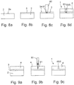
- Figs. 6a-6f illustrate a first variant of a method for producing an inventive tape type superconductor; in each case, cross-sections perpendicular to the longitudinal direction are shown.
- the method starts with a substrate tape 2, for example a steel substrate or a Hastelloy substrate, polished at its surface 2a of the flat side 8, see Fig. 6a .
- a substrate tape 2 for example a steel substrate or a Hastelloy substrate
- On its surface 2a at least one continuous buffer layer 3 is deposited then, see Fig. 6b .
- a laser beam 60 originating from a laser device 61 is applied, compare Fig. 6d .
- the laser beam 60 strongly heats and etches away superconducting material close to the laser spot 62, what results in a groove 63 in the superconductor layer 4, and here also in the buffer layer 3, compare Fig. 6e .
- the space 65 of the groove 63 is then filled with material, here with a non-superconducting metal such as gold or silver, resulting in a barrier structure 5, compare Fig. 6f .
- the tape type superconductor 1 is finished. Note that typically a protection layer or shunt layer is further deposited on the combined surface 64 of the superconductor layer 4 and the barrier structure 5 (not shown).
- Fig. 6f only one barrier structure 5 is included in the cross-section for simplicity, but the tape type superconductor 1 may include other numbers of barrier structures 5 or other arrangements than shown.
- a semi-finished product with a substrate tape 2 at least one continuous buffer layer 3 and a continuous superconductor layer 4, here of YBCO, is produced (see also Figs. 6a-6c above), compare Fig. 7a .
- a beam 70 of gallium ions (Ga + ) is directed, with the gallium ions being provided by an ion gun 71, compare Fig. 7b .
- said ion bombardment should be done under vacuum conditions.
- the material of the superconductor layer 4 is enriched with gallium, thus locally changing the chemical composition in the corresponding space 65.
- the superconducting characteristics get lost, what results in a barrier structure 5 of non-superconducting material in the tape type superconductor 1, compare Fig. 7c .
- Figs. 8a-8d illustrate a third variant of a method for producing a tape type superconductor.
- a continuous buffer layer 3 is deposited, see Fig. 8b .
- the surface 3a of said buffer layer 3 is then locally scratched with a scratching tool 80 at locations intended for barrier structures, thus forming a disturbance pattern 81 on or in the buffer layer 3, see Fig. 8c .
- This is followed by depositing material, here components for YBCO, on the patterned surface 3a, see Fig. 8d .
- the elemental composition of the material of the superconductor layer 4 and the barrier structure 5 are identical here, but the disturbance pattern 81 causes a different phase composition and/or a different crystallinity, resulting in different characteristics with respect to superconductivity.
- the polished surface 2a of the substrate tape 2 may be scratched (or otherwise disturbed).
- the buffer layer (or layers) deposited on top can carry on this disturbance pattern to the surface 3a of the buffer layer 3 then, also resulting in a superconductor layer 4 and barrier structures 5 upon material deposition.
- a semi-finished product with a substrate tape 2 at least one continuous buffer layer 3 and a continuous superconductor layer 4, here of YBCO, is produced (see also Figs. 6a-6c above), compare Fig. 9a .
- the material of the superconductor layer 4 is locally heated by means of a heating device 90, compare Fig. 9b .
- the superconducting material of the superconductor layer 4 degrades and becomes non-superconductive, for example by a non-reversible phase transition. This results in a barrier structure 5 of non-superconducting material in the corresponding space 65 in the tape type superconductor 1, compare Fig. 9c .
- the elemental composition of the originally superconducting material of the superconductor layer 4 does not change upon the heat treatment.
- very strong heating may lead to a thermolysis, with elements evaporating into the surrounding; in this case the elemental composition will change in the space 65 or the barrier structure 5 as compared to the superconductor layer 4.
- the invention proposes a tape type superconductor with a plurality of barrier structures within its superconductor layer.
- the barrier structures are much shorter than the total length of the tape type superconductor, and the barrier structures are arranged subsequent in longitudinal direction, to which they are parallel.
- numerous barrier structures typically 10 or more, often 100 or more, are arranged subsequently in longitudinal direction, but separated from each other by superconducting intermediate regions.
- the barrier structures are arranged at at least one position in width direction, but there may be a plurality of positions in width direction over which the barrier structures are distributed.
- the barrier structures may be distributed in a pattern periodic in longitudinal direction, or may be arranged in a random pattern.
- the barrier structures are non-superconducting or worse superconducting as compared to the superconductor layer.
- the separated barrier structures allow for a decoupling of regions in the superconductor layer, but all regions of the superconductor layer are still interconnected superconductingly. This reduces unwanted induced magnetization, without a substantial reduction of the critical current.
- Inventive tape type superconductors may be used in spools, magnet coils, in particular for NMR magnets, for motors or generators, transformers, fault current limiters or cables, for example.
Landscapes
- Engineering & Computer Science (AREA)
- Manufacturing & Machinery (AREA)
- Chemical & Material Sciences (AREA)
- Ceramic Engineering (AREA)
- Superconductors And Manufacturing Methods Therefor (AREA)
Priority Applications (2)
| Application Number | Priority Date | Filing Date | Title |
|---|---|---|---|
| EP18161977.6A EP3540795A1 (fr) | 2018-03-15 | 2018-03-15 | Supraconducteur de type bande ayant une pluralité de structures barrières allongées |
| US16/354,348 US20190288175A1 (en) | 2018-03-15 | 2019-03-15 | Tape type superconductor with a plurality of elongated barrier structures |
Applications Claiming Priority (1)
| Application Number | Priority Date | Filing Date | Title |
|---|---|---|---|
| EP18161977.6A EP3540795A1 (fr) | 2018-03-15 | 2018-03-15 | Supraconducteur de type bande ayant une pluralité de structures barrières allongées |
Publications (1)
| Publication Number | Publication Date |
|---|---|
| EP3540795A1 true EP3540795A1 (fr) | 2019-09-18 |
Family
ID=61683647
Family Applications (1)
| Application Number | Title | Priority Date | Filing Date |
|---|---|---|---|
| EP18161977.6A Withdrawn EP3540795A1 (fr) | 2018-03-15 | 2018-03-15 | Supraconducteur de type bande ayant une pluralité de structures barrières allongées |
Country Status (2)
| Country | Link |
|---|---|
| US (1) | US20190288175A1 (fr) |
| EP (1) | EP3540795A1 (fr) |
Cited By (1)
| Publication number | Priority date | Publication date | Assignee | Title |
|---|---|---|---|---|
| WO2023194481A1 (fr) * | 2022-04-08 | 2023-10-12 | Tokamak Energy Ltd | Ruban hts à conductance transversale améliorée |
Citations (9)
| Publication number | Priority date | Publication date | Assignee | Title |
|---|---|---|---|---|
| EP0296973A2 (fr) * | 1987-06-22 | 1988-12-28 | Sumitomo Electric Industries Limited | Procédé de réalisation d'un circuit supraconducteur |
| US20050139380A1 (en) * | 2003-12-31 | 2005-06-30 | Superpower, Inc. | Novel superconducting articles, and methods for forming and using same |
| US20070191202A1 (en) | 2005-10-06 | 2007-08-16 | Foltyn Stephen R | Segmented superconducting tape having reduced AC losses and method of making |
| US20080004184A1 (en) * | 2005-09-21 | 2008-01-03 | Kazuya Ohmatsu | Method of Manufacturing Superconducting Tape Wire, Superconducting Tape Wire, and Superconducting Apparatus |
| EP2144255A1 (fr) | 2008-07-09 | 2010-01-13 | European High Temperature Superconductors GmbH & Co. KG | Câble supraconducteur |
| DE102009038920A1 (de) | 2009-08-26 | 2011-03-10 | Siemens Aktiengesellschaft | Multifilamentleiter und Verfahren zu dessen Herstellung |
| EP2490273A1 (fr) | 2011-02-18 | 2012-08-22 | Bruker HTS GmbH | Procédé de fabrication d'une bande revêtue de HTS avec un découpage au faisceau laser |
| US20170287599A1 (en) | 2015-11-06 | 2017-10-05 | Fujikura Ltd. | Oxide superconducting wire |
| US9786415B2 (en) | 2012-07-05 | 2017-10-10 | University Of Houston System | Multi-filament superconducting composites |
-
2018
- 2018-03-15 EP EP18161977.6A patent/EP3540795A1/fr not_active Withdrawn
-
2019
- 2019-03-15 US US16/354,348 patent/US20190288175A1/en not_active Abandoned
Patent Citations (9)
| Publication number | Priority date | Publication date | Assignee | Title |
|---|---|---|---|---|
| EP0296973A2 (fr) * | 1987-06-22 | 1988-12-28 | Sumitomo Electric Industries Limited | Procédé de réalisation d'un circuit supraconducteur |
| US20050139380A1 (en) * | 2003-12-31 | 2005-06-30 | Superpower, Inc. | Novel superconducting articles, and methods for forming and using same |
| US20080004184A1 (en) * | 2005-09-21 | 2008-01-03 | Kazuya Ohmatsu | Method of Manufacturing Superconducting Tape Wire, Superconducting Tape Wire, and Superconducting Apparatus |
| US20070191202A1 (en) | 2005-10-06 | 2007-08-16 | Foltyn Stephen R | Segmented superconducting tape having reduced AC losses and method of making |
| EP2144255A1 (fr) | 2008-07-09 | 2010-01-13 | European High Temperature Superconductors GmbH & Co. KG | Câble supraconducteur |
| DE102009038920A1 (de) | 2009-08-26 | 2011-03-10 | Siemens Aktiengesellschaft | Multifilamentleiter und Verfahren zu dessen Herstellung |
| EP2490273A1 (fr) | 2011-02-18 | 2012-08-22 | Bruker HTS GmbH | Procédé de fabrication d'une bande revêtue de HTS avec un découpage au faisceau laser |
| US9786415B2 (en) | 2012-07-05 | 2017-10-10 | University Of Houston System | Multi-filament superconducting composites |
| US20170287599A1 (en) | 2015-11-06 | 2017-10-05 | Fujikura Ltd. | Oxide superconducting wire |
Cited By (1)
| Publication number | Priority date | Publication date | Assignee | Title |
|---|---|---|---|---|
| WO2023194481A1 (fr) * | 2022-04-08 | 2023-10-12 | Tokamak Energy Ltd | Ruban hts à conductance transversale améliorée |
Also Published As
| Publication number | Publication date |
|---|---|
| US20190288175A1 (en) | 2019-09-19 |
Similar Documents
| Publication | Publication Date | Title |
|---|---|---|
| KR101782177B1 (ko) | 멀티필라멘트 도체 및 그의 제조 방법 | |
| KR101419331B1 (ko) | 감소된 교류 손실들을 갖는 다중필라멘트 초전도체 및 그 형성 방법 | |
| EP2131407A1 (fr) | Câble supraconducteur avec faibles pertes de CA | |
| EP0638942B1 (fr) | Fil en oxyde supraconducteur, procédé de sa fabrication, bobine et câble en oxyde supraconducteur | |
| KR102683995B1 (ko) | 제2세대 초전도성 필라멘트와 케이블 | |
| US11877521B2 (en) | Flexible multi-filament high temperature superconducting cable | |
| JP2960481B2 (ja) | 超電導体テープ中の渦電流の低減方法および超電導体装置 | |
| US20210184096A1 (en) | Fabrication of superconductor wire | |
| Selvamanickam et al. | Scale up of applications-ready practical Y-Ba-Cu-O coated conductors | |
| US11257611B2 (en) | Superconducting wire rod and superconducting coil | |
| EP3540795A1 (fr) | Supraconducteur de type bande ayant une pluralité de structures barrières allongées | |
| US8260387B2 (en) | Superconducting articles and methods of fabrication thereof with reduced AC magnetic field losses | |
| Sato et al. | Development of YBa/sub 2/Cu/sub 3/O/sub y/tape by using inclined substrate method | |
| US20170004913A1 (en) | Dielectric substrate for superconductive device and superconductive article utilizing such substrate | |
| Fukushima et al. | Properties of long GdBCO coated conductor by IBAD-PLD method—The first GdBCO coil test | |
| JP2021018891A (ja) | 高温超伝導線材、その製造方法および製造装置 | |
| RU2824847C1 (ru) | Сверхпроводниковая геликоидальная обмотка | |
| Solovyov et al. | Electromechanical properties of 1-mm-wide superconducting cables comprised of exfoliated YBCO filaments | |
| JP5041414B2 (ja) | 超電導ワイヤーおよび超電導導体 | |
| WO2022070803A1 (fr) | Matériau de fil supraconducteur et câble supraconducteur | |
| Hossain et al. | Development of High Current Capacity Mono-and 18-Filament in situ $\hbox {MgB} _ {2} $ Cables by Varying the Twist Pitch | |
| Ha et al. | Influence of filament number on workability and critical current density of Bi-2212/Ag superconducting wires | |
| Chernoplekov | State of the art in applied high-current superconductivity | |
| JP2022139398A (ja) | 希土類系酸化物超伝導多芯線材、および、その製造方法 | |
| Hasegawa et al. | Superconducting Properties of Bi 2 Sr 2 CaCu 2 O y Tape Prepared by the Continuous Heat Treatment Technique |
Legal Events
| Date | Code | Title | Description |
|---|---|---|---|
| PUAI | Public reference made under article 153(3) epc to a published international application that has entered the european phase |
Free format text: ORIGINAL CODE: 0009012 |
|
| STAA | Information on the status of an ep patent application or granted ep patent |
Free format text: STATUS: THE APPLICATION HAS BEEN PUBLISHED |
|
| AK | Designated contracting states |
Kind code of ref document: A1 Designated state(s): AL AT BE BG CH CY CZ DE DK EE ES FI FR GB GR HR HU IE IS IT LI LT LU LV MC MK MT NL NO PL PT RO RS SE SI SK SM TR |
|
| AX | Request for extension of the european patent |
Extension state: BA ME |
|
| STAA | Information on the status of an ep patent application or granted ep patent |
Free format text: STATUS: REQUEST FOR EXAMINATION WAS MADE |
|
| 17P | Request for examination filed |
Effective date: 20200313 |
|
| RBV | Designated contracting states (corrected) |
Designated state(s): AL AT BE BG CH CY CZ DE DK EE ES FI FR GB GR HR HU IE IS IT LI LT LU LV MC MK MT NL NO PL PT RO RS SE SI SK SM TR |
|
| STAA | Information on the status of an ep patent application or granted ep patent |
Free format text: STATUS: THE APPLICATION IS DEEMED TO BE WITHDRAWN |
|
| 18D | Application deemed to be withdrawn |
Effective date: 20211001 |