EP3540780A1 - Embedded field plate field effect transistor - Google Patents
Embedded field plate field effect transistor Download PDFInfo
- Publication number
- EP3540780A1 EP3540780A1 EP19163154.8A EP19163154A EP3540780A1 EP 3540780 A1 EP3540780 A1 EP 3540780A1 EP 19163154 A EP19163154 A EP 19163154A EP 3540780 A1 EP3540780 A1 EP 3540780A1
- Authority
- EP
- European Patent Office
- Prior art keywords
- type
- deep trench
- disposed
- semiconductor die
- extends
- Prior art date
- Legal status (The legal status is an assumption and is not a legal conclusion. Google has not performed a legal analysis and makes no representation as to the accuracy of the status listed.)
- Granted
Links
Images





Classifications
-
- H—ELECTRICITY
- H10—SEMICONDUCTOR DEVICES; ELECTRIC SOLID-STATE DEVICES NOT OTHERWISE PROVIDED FOR
- H10D—INORGANIC ELECTRIC SEMICONDUCTOR DEVICES
- H10D62/00—Semiconductor bodies, or regions thereof, of devices having potential barriers
- H10D62/10—Shapes, relative sizes or dispositions of the regions of the semiconductor bodies; Shapes of the semiconductor bodies
- H10D62/102—Constructional design considerations for preventing surface leakage or controlling electric field concentration
- H10D62/103—Constructional design considerations for preventing surface leakage or controlling electric field concentration for increasing or controlling the breakdown voltage of reverse-biased devices
- H10D62/105—Constructional design considerations for preventing surface leakage or controlling electric field concentration for increasing or controlling the breakdown voltage of reverse-biased devices by having particular doping profiles, shapes or arrangements of PN junctions; by having supplementary regions, e.g. junction termination extension [JTE]
- H10D62/106—Constructional design considerations for preventing surface leakage or controlling electric field concentration for increasing or controlling the breakdown voltage of reverse-biased devices by having particular doping profiles, shapes or arrangements of PN junctions; by having supplementary regions, e.g. junction termination extension [JTE] having supplementary regions doped oppositely to or in rectifying contact with regions of the semiconductor bodies, e.g. guard rings with PN or Schottky junctions
- H10D62/107—Buried supplementary regions, e.g. buried guard rings
-
- H—ELECTRICITY
- H10—SEMICONDUCTOR DEVICES; ELECTRIC SOLID-STATE DEVICES NOT OTHERWISE PROVIDED FOR
- H10D—INORGANIC ELECTRIC SEMICONDUCTOR DEVICES
- H10D64/00—Electrodes of devices having potential barriers
- H10D64/20—Electrodes characterised by their shapes, relative sizes or dispositions
- H10D64/27—Electrodes not carrying the current to be rectified, amplified, oscillated or switched, e.g. gates
- H10D64/311—Gate electrodes for field-effect devices
- H10D64/411—Gate electrodes for field-effect devices for FETs
- H10D64/511—Gate electrodes for field-effect devices for FETs for IGFETs
- H10D64/512—Disposition of the gate electrodes, e.g. buried gates
- H10D64/513—Disposition of the gate electrodes, e.g. buried gates within recesses in the substrate, e.g. trench gates, groove gates or buried gates
-
- H—ELECTRICITY
- H10—SEMICONDUCTOR DEVICES; ELECTRIC SOLID-STATE DEVICES NOT OTHERWISE PROVIDED FOR
- H10D—INORGANIC ELECTRIC SEMICONDUCTOR DEVICES
- H10D30/00—Field-effect transistors [FET]
- H10D30/60—Insulated-gate field-effect transistors [IGFET]
- H10D30/64—Double-diffused metal-oxide semiconductor [DMOS] FETs
-
- H—ELECTRICITY
- H10—SEMICONDUCTOR DEVICES; ELECTRIC SOLID-STATE DEVICES NOT OTHERWISE PROVIDED FOR
- H10D—INORGANIC ELECTRIC SEMICONDUCTOR DEVICES
- H10D30/00—Field-effect transistors [FET]
- H10D30/60—Insulated-gate field-effect transistors [IGFET]
- H10D30/64—Double-diffused metal-oxide semiconductor [DMOS] FETs
- H10D30/66—Vertical DMOS [VDMOS] FETs
- H10D30/665—Vertical DMOS [VDMOS] FETs having edge termination structures
-
- H—ELECTRICITY
- H10—SEMICONDUCTOR DEVICES; ELECTRIC SOLID-STATE DEVICES NOT OTHERWISE PROVIDED FOR
- H10D—INORGANIC ELECTRIC SEMICONDUCTOR DEVICES
- H10D30/00—Field-effect transistors [FET]
- H10D30/60—Insulated-gate field-effect transistors [IGFET]
- H10D30/64—Double-diffused metal-oxide semiconductor [DMOS] FETs
- H10D30/66—Vertical DMOS [VDMOS] FETs
- H10D30/668—Vertical DMOS [VDMOS] FETs having trench gate electrodes, e.g. UMOS transistors
-
- H—ELECTRICITY
- H10—SEMICONDUCTOR DEVICES; ELECTRIC SOLID-STATE DEVICES NOT OTHERWISE PROVIDED FOR
- H10D—INORGANIC ELECTRIC SEMICONDUCTOR DEVICES
- H10D62/00—Semiconductor bodies, or regions thereof, of devices having potential barriers
- H10D62/10—Shapes, relative sizes or dispositions of the regions of the semiconductor bodies; Shapes of the semiconductor bodies
- H10D62/102—Constructional design considerations for preventing surface leakage or controlling electric field concentration
- H10D62/103—Constructional design considerations for preventing surface leakage or controlling electric field concentration for increasing or controlling the breakdown voltage of reverse-biased devices
- H10D62/105—Constructional design considerations for preventing surface leakage or controlling electric field concentration for increasing or controlling the breakdown voltage of reverse-biased devices by having particular doping profiles, shapes or arrangements of PN junctions; by having supplementary regions, e.g. junction termination extension [JTE]
- H10D62/106—Constructional design considerations for preventing surface leakage or controlling electric field concentration for increasing or controlling the breakdown voltage of reverse-biased devices by having particular doping profiles, shapes or arrangements of PN junctions; by having supplementary regions, e.g. junction termination extension [JTE] having supplementary regions doped oppositely to or in rectifying contact with regions of the semiconductor bodies, e.g. guard rings with PN or Schottky junctions
-
- H—ELECTRICITY
- H10—SEMICONDUCTOR DEVICES; ELECTRIC SOLID-STATE DEVICES NOT OTHERWISE PROVIDED FOR
- H10D—INORGANIC ELECTRIC SEMICONDUCTOR DEVICES
- H10D62/00—Semiconductor bodies, or regions thereof, of devices having potential barriers
- H10D62/10—Shapes, relative sizes or dispositions of the regions of the semiconductor bodies; Shapes of the semiconductor bodies
- H10D62/102—Constructional design considerations for preventing surface leakage or controlling electric field concentration
- H10D62/103—Constructional design considerations for preventing surface leakage or controlling electric field concentration for increasing or controlling the breakdown voltage of reverse-biased devices
- H10D62/105—Constructional design considerations for preventing surface leakage or controlling electric field concentration for increasing or controlling the breakdown voltage of reverse-biased devices by having particular doping profiles, shapes or arrangements of PN junctions; by having supplementary regions, e.g. junction termination extension [JTE]
- H10D62/109—Reduced surface field [RESURF] PN junction structures
- H10D62/111—Multiple RESURF structures, e.g. double RESURF or 3D-RESURF structures
-
- H—ELECTRICITY
- H10—SEMICONDUCTOR DEVICES; ELECTRIC SOLID-STATE DEVICES NOT OTHERWISE PROVIDED FOR
- H10D—INORGANIC ELECTRIC SEMICONDUCTOR DEVICES
- H10D62/00—Semiconductor bodies, or regions thereof, of devices having potential barriers
- H10D62/10—Shapes, relative sizes or dispositions of the regions of the semiconductor bodies; Shapes of the semiconductor bodies
- H10D62/124—Shapes, relative sizes or dispositions of the regions of semiconductor bodies or of junctions between the regions
- H10D62/126—Top-view geometrical layouts of the regions or the junctions
- H10D62/127—Top-view geometrical layouts of the regions or the junctions of cellular field-effect devices, e.g. multicellular DMOS transistors or IGBTs
-
- H—ELECTRICITY
- H10—SEMICONDUCTOR DEVICES; ELECTRIC SOLID-STATE DEVICES NOT OTHERWISE PROVIDED FOR
- H10D—INORGANIC ELECTRIC SEMICONDUCTOR DEVICES
- H10D62/00—Semiconductor bodies, or regions thereof, of devices having potential barriers
- H10D62/10—Shapes, relative sizes or dispositions of the regions of the semiconductor bodies; Shapes of the semiconductor bodies
- H10D62/13—Semiconductor regions connected to electrodes carrying current to be rectified, amplified or switched, e.g. source or drain regions
- H10D62/149—Source or drain regions of field-effect devices
- H10D62/151—Source or drain regions of field-effect devices of IGFETs
- H10D62/152—Source regions of DMOS transistors
- H10D62/154—Dispositions
-
- H—ELECTRICITY
- H10—SEMICONDUCTOR DEVICES; ELECTRIC SOLID-STATE DEVICES NOT OTHERWISE PROVIDED FOR
- H10D—INORGANIC ELECTRIC SEMICONDUCTOR DEVICES
- H10D62/00—Semiconductor bodies, or regions thereof, of devices having potential barriers
- H10D62/10—Shapes, relative sizes or dispositions of the regions of the semiconductor bodies; Shapes of the semiconductor bodies
- H10D62/17—Semiconductor regions connected to electrodes not carrying current to be rectified, amplified or switched, e.g. channel regions
- H10D62/393—Body regions of DMOS transistors or IGBTs
-
- H—ELECTRICITY
- H10—SEMICONDUCTOR DEVICES; ELECTRIC SOLID-STATE DEVICES NOT OTHERWISE PROVIDED FOR
- H10D—INORGANIC ELECTRIC SEMICONDUCTOR DEVICES
- H10D64/00—Electrodes of devices having potential barriers
- H10D64/111—Field plates
- H10D64/112—Field plates comprising multiple field plate segments
-
- H—ELECTRICITY
- H10—SEMICONDUCTOR DEVICES; ELECTRIC SOLID-STATE DEVICES NOT OTHERWISE PROVIDED FOR
- H10D—INORGANIC ELECTRIC SEMICONDUCTOR DEVICES
- H10D64/00—Electrodes of devices having potential barriers
- H10D64/111—Field plates
- H10D64/117—Recessed field plates, e.g. trench field plates or buried field plates
-
- H—ELECTRICITY
- H10—SEMICONDUCTOR DEVICES; ELECTRIC SOLID-STATE DEVICES NOT OTHERWISE PROVIDED FOR
- H10D—INORGANIC ELECTRIC SEMICONDUCTOR DEVICES
- H10D64/00—Electrodes of devices having potential barriers
- H10D64/20—Electrodes characterised by their shapes, relative sizes or dispositions
- H10D64/23—Electrodes carrying the current to be rectified, amplified, oscillated or switched, e.g. sources, drains, anodes or cathodes
- H10D64/251—Source or drain electrodes for field-effect devices
- H10D64/252—Source or drain electrodes for field-effect devices for vertical or pseudo-vertical devices
-
- H—ELECTRICITY
- H10—SEMICONDUCTOR DEVICES; ELECTRIC SOLID-STATE DEVICES NOT OTHERWISE PROVIDED FOR
- H10D—INORGANIC ELECTRIC SEMICONDUCTOR DEVICES
- H10D64/00—Electrodes of devices having potential barriers
- H10D64/20—Electrodes characterised by their shapes, relative sizes or dispositions
- H10D64/27—Electrodes not carrying the current to be rectified, amplified, oscillated or switched, e.g. gates
- H10D64/311—Gate electrodes for field-effect devices
- H10D64/411—Gate electrodes for field-effect devices for FETs
- H10D64/511—Gate electrodes for field-effect devices for FETs for IGFETs
- H10D64/517—Gate electrodes for field-effect devices for FETs for IGFETs characterised by the conducting layers
- H10D64/518—Gate electrodes for field-effect devices for FETs for IGFETs characterised by the conducting layers characterised by their lengths or sectional shapes
-
- H—ELECTRICITY
- H10—SEMICONDUCTOR DEVICES; ELECTRIC SOLID-STATE DEVICES NOT OTHERWISE PROVIDED FOR
- H10D—INORGANIC ELECTRIC SEMICONDUCTOR DEVICES
- H10D64/00—Electrodes of devices having potential barriers
- H10D64/20—Electrodes characterised by their shapes, relative sizes or dispositions
- H10D64/27—Electrodes not carrying the current to be rectified, amplified, oscillated or switched, e.g. gates
- H10D64/311—Gate electrodes for field-effect devices
- H10D64/411—Gate electrodes for field-effect devices for FETs
- H10D64/511—Gate electrodes for field-effect devices for FETs for IGFETs
- H10D64/517—Gate electrodes for field-effect devices for FETs for IGFETs characterised by the conducting layers
- H10D64/519—Gate electrodes for field-effect devices for FETs for IGFETs characterised by the conducting layers characterised by their top-view geometrical layouts
-
- H—ELECTRICITY
- H10—SEMICONDUCTOR DEVICES; ELECTRIC SOLID-STATE DEVICES NOT OTHERWISE PROVIDED FOR
- H10D—INORGANIC ELECTRIC SEMICONDUCTOR DEVICES
- H10D84/00—Integrated devices formed in or on semiconductor substrates that comprise only semiconducting layers, e.g. on Si wafers or on GaAs-on-Si wafers
- H10D84/01—Manufacture or treatment
- H10D84/0123—Integrating together multiple components covered by H10D12/00 or H10D30/00, e.g. integrating multiple IGBTs
- H10D84/0126—Integrating together multiple components covered by H10D12/00 or H10D30/00, e.g. integrating multiple IGBTs the components including insulated gates, e.g. IGFETs
- H10D84/0156—Manufacturing their doped wells
-
- H—ELECTRICITY
- H10—SEMICONDUCTOR DEVICES; ELECTRIC SOLID-STATE DEVICES NOT OTHERWISE PROVIDED FOR
- H10W—GENERIC PACKAGES, INTERCONNECTIONS, CONNECTORS OR OTHER CONSTRUCTIONAL DETAILS OF DEVICES COVERED BY CLASS H10
- H10W10/00—Isolation regions in semiconductor bodies between components of integrated devices
- H10W10/01—Manufacture or treatment
- H10W10/011—Manufacture or treatment of isolation regions comprising dielectric materials
- H10W10/014—Manufacture or treatment of isolation regions comprising dielectric materials using trench refilling with dielectric materials, e.g. shallow trench isolations
- H10W10/0143—Manufacture or treatment of isolation regions comprising dielectric materials using trench refilling with dielectric materials, e.g. shallow trench isolations comprising concurrently refilling multiple trenches having different shapes or dimensions
-
- H—ELECTRICITY
- H10—SEMICONDUCTOR DEVICES; ELECTRIC SOLID-STATE DEVICES NOT OTHERWISE PROVIDED FOR
- H10D—INORGANIC ELECTRIC SEMICONDUCTOR DEVICES
- H10D62/00—Semiconductor bodies, or regions thereof, of devices having potential barriers
- H10D62/10—Shapes, relative sizes or dispositions of the regions of the semiconductor bodies; Shapes of the semiconductor bodies
- H10D62/13—Semiconductor regions connected to electrodes carrying current to be rectified, amplified or switched, e.g. source or drain regions
- H10D62/149—Source or drain regions of field-effect devices
- H10D62/151—Source or drain regions of field-effect devices of IGFETs
- H10D62/156—Drain regions of DMOS transistors
- H10D62/157—Impurity concentrations or distributions
-
- H—ELECTRICITY
- H10—SEMICONDUCTOR DEVICES; ELECTRIC SOLID-STATE DEVICES NOT OTHERWISE PROVIDED FOR
- H10W—GENERIC PACKAGES, INTERCONNECTIONS, CONNECTORS OR OTHER CONSTRUCTIONAL DETAILS OF DEVICES COVERED BY CLASS H10
- H10W72/00—Interconnections or connectors in packages
- H10W72/90—Bond pads, in general
- H10W72/921—Structures or relative sizes of bond pads
- H10W72/926—Multiple bond pads having different sizes
Definitions
- the described embodiments relate to power field effect transistors and to related methods.
- trench power field effect transistors also called power trench MOSFETs
- a type of trench power MOSFET involving a "buried field plate” is being popularized.
- This type of trench power MOSFET goes by various other names.
- the term “buried source”, for example, is also sometimes used.
- the term “RESURF” is also used in connection with this type of trench power MOSFET.
- the buried field plate transistor is a trench MOSFET that has an especially deep trench. Within this deep trench, along with the gate, is a vertically-oriented conductive buried field plate.
- This buried field plate is typically disposed below the gate so that it extends along the inside side surfaces of the deepest parts of the deep trench.
- the buried field plate like the gate above it, is separated from the semiconductor material of the trench sidewall by an insulative dielectric layer. Due to its placement, the buried field plate extends along and adjacent to the drift zone in the N- type semiconductor material that is immediately outside the deep trench. This drift zone is an amount of N- type semiconductor material disposed underneath the P type body region of the transistor.
- the semiconductor portion of a trench power N-channel field effect transistor die has plurality of deep trenches cut into its topside semiconductor surface.
- a first of these deep trenches extends in a first straight line parallel to a side edge of the die.
- a second of these deep trenches extends in a second straight line parallel to the first straight line, such that the first deep trench is disposed between the second deep trench and the side edge of the die.
- These two deep trenches extend parallel to each other, and parallel to the side edge of the die. There may be more such parallel extending deep trenches, but there are at least these two.
- a third deep trench extends in a third straight line perpendicular to the side edge of the die. This third deep trench terminates into the second deep trench.
- a fourth deep trench extends in a fourth straight line perpendicular to the side edge of the die.
- the fourth deep trench also terminates into the second deep trench.
- the third and fourth deep trenches extend parallel to one another, and there is no deep trench between them.
- the trench power N-channel field effect transistor die also has an embedded field plate structure. In one example, a first part of this embedded field plate structure is disposed at least partly in the first deep trench, a second part of this embedded field plate structure is disposed at least partly in the second deep trench, a third part of this embedded field plate structure is disposed at least partly in the third deep trench, and a fourth part of this embedded field plate structure is disposed at least partly in the fourth deep trench.
- the trench power N-channel field effect transistor die has an edge area and an active area.
- the edge area is disposed adjacent the side edge of the die. There are no gates or N+ type source regions in this edge area.
- the active area on other hand, has gates and N+ type source regions.
- the edge area is disposed between the active area of the die and the die side edge.
- the semiconductor portion of the die involves a bottom N++ type substrate layer. Disposed on that N++ type substrate layer is an N- type drift layer that extends up to the topside semiconductor surface.
- This N- type drift layer has a lower layer portion, and a more highly doped N- type upper layer portion. The deep trenches cut into the N- type upper layer portion and extend down through the N- type upper layer portion so that they just penetrate the top of the N- type lower layer portion.
- a P type body region In the active area, between the third and fourth deep trenches, is a P type body region. This P type body region extends down into the N- type drift layer from the topside semiconductor surface.
- the N+ type source region is disposed between the third and fourth deep trenches in the active area.
- the P type body region also extends laterally from the active area (through a gate bus line and embedded field plate grounding area) and into the edge area.
- the trench power N-channel field effect transistor die has a topside source metal electrode structure, a topside gate metal electrode structure, and a bottomside drain metal electrode structure.
- the source metal electrode structure is coupled to the N+ type source region or regions of the active area, and is also coupled to the P type body region or regions of the active area.
- the gate metal electrode structure is coupled to the gate or gates of the active area.
- the drain metal electrode structure is disposed on the bottom of the semiconductor portion of the die so that it is coupled to the bottomside semiconductor surface, and is in contact with the N++ type substrate layer.
- the trench power N-channel field effect transistor die includes a first floating P type well region and a second floating P type well region.
- the first floating P type well region extends down into the N- type drift layer from the topside semiconductor surface. It is disposed entirely in the edge area of the semiconductor die structure, and entirely between the third and fourth deep trenches.
- the second floating P type well region extends down into the N- type drift layer from the topside semiconductor surface. It is disposed entirely in the edge area of the semiconductor die structure, and entirely between the third and fourth deep trenches.
- the first and second floating P type well regions are disposed such that they are disposed along a fifth straight line.
- the fifth straight line extends perpendicularly from the side edge of the semiconductor die structure, and extends transversely through the first and second deep trenches, and extends between the third and fourth trenches, and into the active area of the semiconductor die structure.
- This fifth line is parallel to the third straight line of the third deep trench and is also parallel to the fourth straight line of the fourth deep trench.
- the first and second floating P type well regions are disposed along this fifth straight line between the P type body region and the second deep trench.
- the first floating P type well region is the outer of the two (the one closest to the die side edge), and this first floating P type well region forms a part of an inner sidewall of the second deep trench.
- These first and second floating P type well regions are "floating" in the sense that they are not coupled to the source electrode structure, the drain electrode structure, or the gate electrode structure of the overall MOSFET device. In a situation of a large voltage on the drain electrode structure with respect to the source electrode structure, the first and second floating P type well regions serve to prevent avalanche breakdown in the edge area.
- the trench power N-channel field effect transistor die would suffer avalanche breakdown in the edge area near the second deep trench were a set of floating P type well regions (including the first and second floating P type well regions) not provided.
- the overall trench power N-channel field effect transistor die does not suffer avalanche breakdown first in the edge area, but rather it suffers avalanche breakdown first in the active area. Accordingly, the drain-to-source breakdown voltage BVDSS of the overall transistor device is increased.
- N type silicon can be generally referred to simply as N type silicon or it can be more specifically referred to as N++ type silicon, N+ type silicon, N type silicon, or N- type silicon.
- the N++, N+, N and N- designators are intended to designate relative ranges of dopant concentrations in a rough general sense.
- N- type silicon there may, for example, be an overlap in the ranges of concentrations between silicon described as N- type silicon and silicon described as N type silicon.
- the dopant concentration at the bottom of the N+ type silicon range may be lower than the dopant concentration at the top of the N type silicon range.
- P type silicon in terms of sometimes more specifically referring to P++ type silicon, P+ type silicon, P type silicon, or P- type silicon is also employed in this patent document.
- FIG. 1 is a top-down diagram of a semiconductor die structure 1 in accordance with one novel aspect.
- This semiconductor die structure 1 is an embedded field plate N-channel field effect transistor die, also known as an EFP MOSFET. "EFP” stands for "Embedded Field Plate”.
- Semiconductor die structure 1 has four peripheral side edges 2-5 when the die structure is considered from the top-down perspective.
- a source metal electrode structure 26 On the top of the die structure is a source metal electrode structure 26, a metal source pad 6 which is a part of the source metal electrode structure 26, a metal gate electrode structure 25, a gate pad 7 which is a part of the metal gate structure 25, a body metal structure 27, and a metal depletion stopper ring (not shown).
- the metal depletion stopper ring is another ring of metal that encircles the body metal structure and that extends along the for peripheral side edges of the die structure.
- the gate electrode structure is placed between the body metal and the source electrode in order to be able to make the gate electrode structure a loop.
- Making the gate electrode structure have a loop shape promotes more even gate signal distribution.
- the separation between the source metal and the body metal would provide some resistance in this current path, which is desirable and improves device ruggedness.
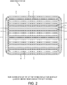
- FIG. 2 is a simplified top-down diagram of the semiconductor die structure 1 of FIG. 1 , except that in the illustration of FIG. 2 the structure above the level of the topside semiconductor surface is not shown.
- the portions of the die structure that are shown as white in FIG. 2 are the topside semiconductor surface.
- the shaded portions are a plurality of deep trenches and any structures in them such as embedded field plates.
- a first peripheral deep trench 6 This first peripheral deep trench 6 extends in a first straight line in the vertical dimension in the illustration in parallel with the right side edge 2 of the die structure.
- Reference numeral 7 indicates a second peripheral deep trench. This second peripheral deep trench 7 extends around the edges of the die but is inside the first peripheral deep trench 6.
- This second peripheral deep trench 7 extends in a second straight line along the right side edge 2 of the die structure.
- Reference numeral 8 identifies a third deep trench.
- This third deep trench 8 extends in a third straight line. Its left end terminates at a location into the deep trench 7 on the left of the die structure. Its right end terminates at another location into the deep trench 7 on the right of the die structure.
- the fourth deep trench 9 extends in a straight line. Its left end terminates at a location into the deep trench 7 on the left of the die structure. Its right end terminates at another location into the deep trench 7 on the right of the die structure.
- the third and fourth deep trenches 8 and 9 extend parallel to each other across the center part of the die as illustrated.
- Deep trenches 8 and 9 are referred to as being separate deep trenches even though the three trenches 7, 8 and 9 actually merge together to form a single deep trench structure.
- the deep trenches are illustrated in FIG. 2 to be fairly wide in order to clarify the illustration. In actuality, there are many more horizontally extending deep trenches, and these deep trenches are much more narrow than the trenches illustrated. Not only are the deep trenches much more narrow than the trenches illustrated in FIG. 2 , but there is also much less separation between adjacent ones of the deep trenches.
- Located in the center of each deep trench is an embedded field plate structure. This embedded field plate structure is not shown in FIG. 2 .
- the active area 10 of the die structure there are gate structures and other structures that extend up to the topside semiconductor surface 17 that are not illustrated. These other structures are not shown in FIG. 2 in order to simplify the diagram.
- FIG. 3 is a diagram of the upper right corner portion of the die structure 1. In this diagram, more deep trenches are shown and the deep trenches that are shown have a tighter spacing.
- the diagram is provided to point out three areas, namely an active area 10, a gate bus line and embedded field plate grounding area 11, and an edge area 12.
- Sectional line A-A' is a sectional line taken at the left side of the active area 10.
- Sectional line B-B' is a sectional line taken at the bottom side of the edge area 12.
- FIG. 4 is a diagram similar to FIG. 3 , except that FIG. 4 shows where a sectional line C-C' is taken. Sectional line C-C' is taken at the left side of edge area 12.
- FIG. 5 is a cross-sectional diagram taken along sectional line A-A' of FIG. 3 .
- the deep trench shown at the left is the third deep trench 8.
- the deep trench shown to the right is the fourth deep trench 9.
- a part 13A of a gate structure 13 extends into the third deep trench 8 at the left, and a part 13B of the gate structure 13 extends into the fourth deep trench 9 at the right.
- These parts 13A and 13B of the gate structure 13 are features of N+ type polysilicon.
- the overall gate structure is identified by reference numeral 13.
- Reference numerals 14A and 14B identify parts of an embedded field plate structure 14.
- the embedded field plate structure 14 is a structure of N+ type polysilicon.
- An N- type drift layer 15 is disposed on an N++ type substrate layer 16.
- the N++ type substrate layer 16 is monocrystalline wafer material whereas the N- type drive layer is typically epitaxial silicon.
- the N- type drift layer 15 in turn includes a lower layer portion 15A and an upper layer portion 15B.
- the upper layer portion 15B of the N- type drift layer has a higher concentration of N type dopants than does the lower layer portion 15A of the N-type drift layer.
- the N- type drift layer 15 is labeled as extending all the way up to the topside semiconductor surface 17 because it does extend up to this surface outside of the plane of the illustration.
- the deep trenches extend down from the topside semiconductor surface 17, and extend through the upper layer portion 15B of the N- type drift layer, and into the top of the lower layer portion 15A of the N- type drift layer.
- Reference numeral 32 identifies insulative dielectric material in the deep trenches. This insulative dielectric material 32 is typically thermal silicon oxide.
- This insulative dielectric material 32 separates the semiconductor sidewalls of the deep trenches from the parts of the gate structure 13 and from the parts of the embedded field plate structure 14.
- Reference numeral 18 identifies the bottomside semiconductor surface.
- P type body regions extend downward from the topside semiconductor surface 17 as shown.
- Reference numeral 19 at the right of FIG. 5 identifies one of the P type body regions.
- a set of N+ type source regions extends downward from the topside semiconductor surface 17 into the P type body regions as shown.
- One of these N+ type source regions is identified by reference numeral 20.
- These N+ type source regions have a ladder shape when considered from the top-down perspective. The ladder shape involves two parallel-extending sides, and a set of spanning rungs.
- Source metal structure 26 is coupled to the top of such an N+ type source region at its rung areas. These connection points between the source metal electrode 26 and the N+ type source regions are not present in the particular cross-section of FIG. 5 .
- the source metal electrode structure 26 is also coupled to the P type body regions by P+ type body contact regions.
- source metal structure 26 is coupled to P type body region 19 at the right of FIG. 5 by P+ type body contact region 22.
- Insulative dielectric features 23A and 23B separate the source metal electrode 26 from the gate structure 13.
- the gate bus line and electrode 25 structure (see FIG. 1 ) on the top of the die structure is not seen in the particular cross-section of FIG. 5 , but the gate bus line structure 25 is coupled by connections elsewhere on the die to the N+ type polysilicon of the gate structure 13.
- a drain metal electrode structure 24 is disposed on the bottomside semiconductor surface 18.
- a conductive channel forms at the edge of the trench adjacent the gate structure.
- This channel extends vertically downward from the N+ type source region, through the P type body region, and to the underlying N- type material of the N- type drift layer 15.
- electrons can flow from the N+ type source region, vertically down through this conductive channel, and to the N- type drift layer 15, through the N- type drift layer 15, and through the N++ type substrate layer 16, and to the drain metal electrode 24.
- the channel is illustrated by arrow 28.
- the embedded field plate within the deep trench extends downward starting from a starting point at or very near to the topside semiconductor surface 17 and extending downward through the center of the deep trench to a depth that is close to the depth of the upper layer portion 15B of the N- type drift layer 15.
- the gate structure has a first downward extending portion that extends downward along the boundary between one side edge of the deep trench and a P type body region on that side of the deep trench, and also has a second downward extending portion that extends downward along the boundary between an opposite side edge of the deep trench and the P type body region on that side of the deep trench.
- reference numeral 13BA identifies one such first downward extending portion of the gate structure portion in deep trench 9
- reference numeral 13BB identifies one such second downward extending portion of the gate structure in deep trench 9.
- the two downward extending portions 13BA and 13BB are connected together at the top by a bridge portion 13BC of the gate structure.
- This bridge portion 13BC is disposed above the topside semiconductor surface 17, and it bridges and spans over the top extent of the embedded field plate portion 14B as shown in FIG. 5 .
- the two downward extending portions 13BA and 13BB and the bridge portion 13BC are all fashioned from the same layer of N+ type polysilicon.
- layer here refers to a contiguous amount of polysilicon, where that polysilicon is polysilicon that was deposited in the same polysilicon deposition step. In this sense, portions 13BA, 13BB and 13BC are one layer of polysilicon.
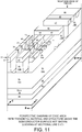
- FIG. 6 is a perspective diagram of the part of the active area illustrated in cross-section in FIG. 5 .
- Two rung portions 20A and 20B of the ladder-shaped N+ type source region 20 are seen in the structure of FIG. 16 .
- the rung portions are actually parts of the overall N+ type source region 20.
- FIG. 7 is a perspective diagram of the structure of FIG. 6 , but with the trench fill material not shown and with the structure above the topside semiconductor surface not shown.
- the ladder-shaped N+ type source regions are seen from this perspective. Between the rungs of a ladder-shaped N+ type source region are P+ type body contact regions.
- FIG. 8 is a cross-sectional diagram taken along sectional line C-C' of the edge area 12 of FIG. 3 and FIG. 4 .
- the drain metal electrode 24, the N++ type substrate layer 16, and lower layer portion 15A of the N- type drift layer 15, and the upper layer portion 15B of the N- type drift layer 15 are the same structures as in the cross-section of the active area 10 of FIG. 5 .
- Reference numerals 29, 30 and 31 identify extensions of P type body regions of the active area.
- P type body region extension 30 is an extension of the P type body region 50.
- Reference numeral 14 identifies the embedded field plate layer of N+ type polysilicon. This is the same N+ type polysilicon layer that makes the embedded field plate portions 14A and 14B of FIG. 5 .
- the embedded field plate structure of FIG. 8 and the embedded field plate structures of FIG. 5 are all different parts of the same one amount of N+ type polysilicon.
- the body metal 27 at the top of FIG. 8 is the same body metal 27 shown in FIG. 1 .
- Reference numeral 32 identifies a feature of a trench-fill insulative dielectric layer. This is the same layer of trench-fill insulative dielectric that forms the trench-fill insulative dielectric features 23A and 23B in the active area shown in FIG. 5 .
- the insulative dielectric layer 33 of FIG. 8 is the same insulative dielectric layer as identified by reference numeral 23 in the cross-section of FIG. 5 .
- the gate structure 13 does not extend into the edge area 12.
- FIG. 9 is a perspective diagram of the edge area 12.
- FIG. 10 is a perspective diagram of the structure of FIG. 9 , but with the body metal 27 not shown.
- FIG. 11 is a perspective diagram of the structure of FIG. 10 , but with the trench fill material not shown and with the structure above the topside semiconductor surface 17 not shown.
- This diagram reveals many isolated and floating P type regions 34-49. Each of these floating P type regions is entirely separate from each of the others. Each of these P type regions is floating, and is not coupled to the source electrode structure of the die, nor to the drain electrode structure of the die, nor to the gate electrode structure of the die.
- the P type regions 46-49 are actually concentric ring-shaped structures that ring around the periphery of the die structure 1 when the die structure 1 is considered from the top-down perspective.
- P type regions 44, 41, 38, 35 and 30 are entirely disposed between the between the third deep trench 8 (see FIG. 2 ) and the fourth deep trench 9 (see FIG. 2 ).
- the P type regions 44, 41, 38 and 35 are disposed entirely between the active area 10 (see FIG. 1 ) and the right side edge 2 of the die (see FIG. 1 ).
- FIG. 12 is a simplified top-down diagram that illustrates the relative positions of various features and structures of the semiconductor die structure 1 of FIG. 1 .
- the deep trench 6 extends in a first straight line parallel to the side edge 2 of the die.
- the deep trench 7 extends in a second straight line parallel to the first line.
- Deep trenches 6 and 7 are a pair of deep trenches that extend parallel to one another, and parallel to the side edge 2.
- Deep trench 8 is a third deep trench that extends in a third straight line.
- the third line is perpendicular to the side edge 2.
- Deep trench 9 is a fourth deep trench that extends in a fourth straight line.
- the fourth line is parallel to the third line.
- Deep trenches 8 and 9 are a pair of deep trenches that extend parallel to one another, and perpendicular to the side edge 2.
- the third deep trench 8 terminates into the second deep trench 7.
- the fourth deep trench 9 terminates into the second deep trench 7.
- These deep trenches 6, 7, 8 and 9 are the same deep trenches as illustrated in FIG. 2 and as described in the text above.
- P type regions 31, 30 and 29 are not floating, but rather they are connected to the source metal in the active area.
- the embedded field plate structure 14 is disposed at least partly in the four deep trenches 6, 7, 8 and 9. A first part of the embedded field plate structure 14 is disposed at least partly in the first deep trench 6. A second part of the embedded field plate structure 14 is disposed at least partly in the second deep trench 7. A third part of the embedded field plate structure 14 is disposed at least partly in the third deep trench 8. A fourth part of the embedded field plate structure 14 is disposed at least partly in the fourth deep trench 9.
- the P type body region 50 is disposed in the active area 12, but it has an extension 30 that extends laterally through the gate bus line and embedded field plate grounding area 11, and into the edge area 12.
- the P type body region 50 is also disposed entirely between the third and fourth deep trenches 8 and 9.
- the N+ type source region 51 is disposed entirely in the active area 12 and between the third and fourth deep trenches.
- the portion 13A of the gate structure 13 is disposed at least partly in the third deep trench 8 in the active area 10, and the portion 13B of the gate structure 13 is disposed at least partly in the fourth deep trench 9 in the active area 10. No part of the gate structure 13 extends into the edge area 12 of the die.
- Each of the floating P type regions 44, 41, 38 and 35 is disposed entirely between the third and fourth deep trenches, and entirely within the edge area 12 of the die.
- the constituent parts of the structure of FIG. 12 are oriented such that the P type regions 44, 41, 38, 35 and 30 are disposed along a fifth straight line 52.
- the fifth straight line 52 extends perpendicularly to the side edge 2, and extends from the side edge 2, and then extends transversely through the first deep trench 6, and then extends transversely through the second deep trench 7, and then extends between the third deep trench 8 and the fourth deep trench 9, and into the active area 12 of the die.
- the P type regions 44, 41, 38, 35 and 30 are disposed along this fifth straight line 52 as illustrated in FIG. 12 between the side edge 2 and the active area 10.
- FIG. 13 and FIG. 14 illustrate and explain an alternative semiconductor die structure that has a different edge area structure.
- the alternative semiconductor die structure has a single P type region 57.
- This single P type region 57 extends outwardly from the location of the A-A' section of FIG. 3 all the way to the second deep trench 7.
- the alternative semiconductor die structure is the same as the novel semiconductor die structure of FIG. 1 .
- the horizontal axis of the diagram of FIG. 13 sets forth the half width of the unit cell of the semiconductor die structure.
- the line 53 which is denoted with squares, indicates how the breakdown voltage of the active area varies as a function of unit cell half width.
- the line 54 which is denoted with circles, is a simulation result that indicates how the breakdown voltage of the edge area varies as a function of unit cell half width.
- the alternative semiconductor die structure was simulated to suffer avalanche breakdown in the location indicated by the star 58 at a breakdown voltage BVDSS of 153 volts.
- the breakdown voltage BVDSS of the overall N-channel field effect transistor die is therefore lower than it otherwise could be were the device not to break down first in its edge area.
- the breakdown voltage BVDSS of the overall N-channel field effect transistor die is the lower of the two lines of FIG. 13 at the location of the 2.0 unit cell half width.
- FIG. 15 and FIG. 16 illustrate and explain a relative advantage of the novel structure of the edge area 12 of the novel semiconductor die structure 1.
- the line 55 which is denoted with squares, shows how the breakdown voltage of the active area varies as a function of unit cell half width.
- the line 56 which is denoted with triangles, shows how the breakdown voltage of the edge area varies as a function of unit cell half width.
- the breakdown voltage of the overall semiconductor die structure is determined by the breakdown voltage of the active area because the breakdown voltage of the edge area (as indicated by line 56) is greater than the breakdown voltage of the active area.
- the line 56 is higher than is the line 55.
- the zero volt potential on the leftmost P type region 30 therefore does not extend laterally to the right all the way to the left edge of the second deep trench 7 due to there being a single conductive P type region spanning this distance. Rather, the 167 volt difference can drop across this lateral distance.
- the voltages on the P type regions 30, 35, 38, 41 and 44 are zero volts, six volts, twelve volts, eighteen volts, and twenty-four volts, respectively. This means that the relative voltage at the left edge of the second deep trench 7 in the case of the structure of FIG. 16 is only 143 volts even though there is a larger 167 volt difference between the drain metal electrode 24 with respect to the source metal electrode 26.
- the overall semiconductor die structure is simulated to have a breakdown voltage BVDSS of 167 volts. Due to limitations of simulation software, the line 56 is actually a simulation of a similar structure that does not have three planar sidewalls (sidewall of trenches 7, 8 and 9) but rather has a half-cylindrical radius sidewall structure.
- the teachings of this patent document have general applicability and are not limited to the specific embodiments described above.
- a particular gate structure and embedded field plate structure is shown in the deep trenches, in other embodiments other gate structures and other embedded field plate structures are used.
- Utility of the floating P type well regions 44, 41, 38 and 35 between the active area and the peripheral deep trenches is not limited to a particular gate structure/embedded field plate design.
- the embedded field plate can have a different form in the active area as compared to the form it has in the edge area.
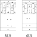
- the structure of FIG. 17 can be employed in the active area and the structure of FIG. 18 can be employed in the edge area.
- FIG. 17 can be employed in the active area
- the structure of FIG. 18 can be employed in the edge area.
- the embedded field plate is disposed entirely below the bottom extent of the gate structure.
- the bottom extent of the gate structure is at or slightly below the bottom extent of the P type body regions.
- the floating P type well regions 44, 41, 38 and 35 can be employed with these types of buried field plate structures as well. Accordingly, various modifications, adaptations, and combinations of various features of the described embodiments can be practiced without departing from the scope of the invention as set forth in the claims.
Landscapes
- Electrodes Of Semiconductors (AREA)
- Insulated Gate Type Field-Effect Transistor (AREA)
- Chemical & Material Sciences (AREA)
- Composite Materials (AREA)
Abstract
Description
- The described embodiments relate to power field effect transistors and to related methods.
- In order to increase the drain-to-source voltage at which a trench power field effect transistors (also called power trench MOSFETs) first suffer avalanche breakdown, a type of trench power MOSFET involving a "buried field plate" is being popularized. This type of trench power MOSFET goes by various other names. The term "buried source", for example, is also sometimes used. The term "RESURF" is also used in connection with this type of trench power MOSFET. In a typical structure, the buried field plate transistor is a trench MOSFET that has an especially deep trench. Within this deep trench, along with the gate, is a vertically-oriented conductive buried field plate. This buried field plate is typically disposed below the gate so that it extends along the inside side surfaces of the deepest parts of the deep trench. The buried field plate, like the gate above it, is separated from the semiconductor material of the trench sidewall by an insulative dielectric layer. Due to its placement, the buried field plate extends along and adjacent to the drift zone in the N- type semiconductor material that is immediately outside the deep trench. This drift zone is an amount of N- type semiconductor material disposed underneath the P type body region of the transistor. By coupling the buried field plate to the source electrode of the transistor, the breakdown voltage BVDSS of the transistor can be increased for a given RDS(ON) and integrated circuit size as compared to the same basic trench MOSFETs structure without the buried field plate. There are many variations on this general transistor structure.
- The semiconductor portion of a trench power N-channel field effect transistor die has plurality of deep trenches cut into its topside semiconductor surface. A first of these deep trenches extends in a first straight line parallel to a side edge of the die. A second of these deep trenches extends in a second straight line parallel to the first straight line, such that the first deep trench is disposed between the second deep trench and the side edge of the die. These two deep trenches extend parallel to each other, and parallel to the side edge of the die. There may be more such parallel extending deep trenches, but there are at least these two. In addition, a third deep trench extends in a third straight line perpendicular to the side edge of the die. This third deep trench terminates into the second deep trench. A fourth deep trench extends in a fourth straight line perpendicular to the side edge of the die. The fourth deep trench also terminates into the second deep trench. The third and fourth deep trenches extend parallel to one another, and there is no deep trench between them. The trench power N-channel field effect transistor die also has an embedded field plate structure. In one example, a first part of this embedded field plate structure is disposed at least partly in the first deep trench, a second part of this embedded field plate structure is disposed at least partly in the second deep trench, a third part of this embedded field plate structure is disposed at least partly in the third deep trench, and a fourth part of this embedded field plate structure is disposed at least partly in the fourth deep trench.
- When considered from the top-down perspective, the trench power N-channel field effect transistor die has an edge area and an active area. The edge area is disposed adjacent the side edge of the die. There are no gates or N+ type source regions in this edge area. The active area, on other hand, has gates and N+ type source regions. The edge area is disposed between the active area of the die and the die side edge.
- When considered from a cross-sectional side view perspective, the semiconductor portion of the die involves a bottom N++ type substrate layer. Disposed on that N++ type substrate layer is an N- type drift layer that extends up to the topside semiconductor surface. This N- type drift layer has a lower layer portion, and a more highly doped N- type upper layer portion. The deep trenches cut into the N- type upper layer portion and extend down through the N- type upper layer portion so that they just penetrate the top of the N- type lower layer portion.
- In the active area, between the third and fourth deep trenches, is a P type body region. This P type body region extends down into the N- type drift layer from the topside semiconductor surface. The N+ type source region is disposed between the third and fourth deep trenches in the active area. The P type body region also extends laterally from the active area (through a gate bus line and embedded field plate grounding area) and into the edge area.
- The trench power N-channel field effect transistor die has a topside source metal electrode structure, a topside gate metal electrode structure, and a bottomside drain metal electrode structure. The source metal electrode structure is coupled to the N+ type source region or regions of the active area, and is also coupled to the P type body region or regions of the active area. The gate metal electrode structure is coupled to the gate or gates of the active area. The drain metal electrode structure is disposed on the bottom of the semiconductor portion of the die so that it is coupled to the bottomside semiconductor surface, and is in contact with the N++ type substrate layer.
- In addition, the trench power N-channel field effect transistor die includes a first floating P type well region and a second floating P type well region. The first floating P type well region extends down into the N- type drift layer from the topside semiconductor surface. It is disposed entirely in the edge area of the semiconductor die structure, and entirely between the third and fourth deep trenches. Likewise, the second floating P type well region extends down into the N- type drift layer from the topside semiconductor surface. It is disposed entirely in the edge area of the semiconductor die structure, and entirely between the third and fourth deep trenches.
- The first and second floating P type well regions are disposed such that they are disposed along a fifth straight line. The fifth straight line extends perpendicularly from the side edge of the semiconductor die structure, and extends transversely through the first and second deep trenches, and extends between the third and fourth trenches, and into the active area of the semiconductor die structure. This fifth line is parallel to the third straight line of the third deep trench and is also parallel to the fourth straight line of the fourth deep trench. The first and second floating P type well regions are disposed along this fifth straight line between the P type body region and the second deep trench. In one example, the first floating P type well region is the outer of the two (the one closest to the die side edge), and this first floating P type well region forms a part of an inner sidewall of the second deep trench. These first and second floating P type well regions are "floating" in the sense that they are not coupled to the source electrode structure, the drain electrode structure, or the gate electrode structure of the overall MOSFET device. In a situation of a large voltage on the drain electrode structure with respect to the source electrode structure, the first and second floating P type well regions serve to prevent avalanche breakdown in the edge area. In one example, the trench power N-channel field effect transistor die would suffer avalanche breakdown in the edge area near the second deep trench were a set of floating P type well regions (including the first and second floating P type well regions) not provided. By providing this set of floating P type well regions, the overall trench power N-channel field effect transistor die does not suffer avalanche breakdown first in the edge area, but rather it suffers avalanche breakdown first in the active area. Accordingly, the drain-to-source breakdown voltage BVDSS of the overall transistor device is increased.
- Further details and embodiments and methods are described in the detailed description below. This summary does not purport to define the invention. The invention is defined by the claims.
- The accompanying drawings, where like numerals indicate like components, illustrate embodiments of the invention.
-
FIG. 1 is a top-down diagram of asemiconductor die structure 1 in accordance with one novel aspect. -
FIG. 2 is a simplified top-down diagram that shows the deep trenches in the topside semiconductor surface of the semiconductor diestructure 1 ofFIG. 1 . -
FIG. 3 is a diagram of the upper right corner portion of thedie structure 1 that shows the active area, the gate bus line and embedded field plate grounding area, and the edge area. -
FIG. 4 is a diagram similar toFIG. 3 , except thatFIG. 4 shows where a sectional line C-C' is taken. -
FIG. 5 is a cross-sectional diagram taken along sectional line A-A' ofFIG. 3 . -
FIG. 6 is a perspective diagram of the part of the active area illustrated in cross-section inFIG. 5 . -
FIG. 7 is a perspective diagram of the structure ofFIG. 6 , but with the trench fill material not shown and with the structure above the topside semiconductor surface not shown. -
FIG. 8 is a cross-sectional diagram taken along sectional line C-C' of theedge area 12 ofFIG. 3 and FIG. 4 . -
FIG. 9 is a perspective diagram of the edge area ofFIG. 8 . -
FIG. 10 is a perspective diagram of the structure ofFIG. 9 , but with the body metal not shown. -
FIG. 11 is a perspective diagram of the structure ofFIG. 10 , but with the trench fill material not shown and with the structure above thetopside semiconductor surface 17 not shown. -
FIG. 12 is a simplified top-down diagram that illustrates the relative positions of various features and structures of the semiconductor diestructure 1 ofFIG. 1 . -
FIG. 13 is a graph that shows how breakdown voltage varies with unit cell half width for the alternative semiconductor die structure ofFIG. 14 . -
FIG. 14 illustrates an alternative semiconductor die structure that has a different edge area structure. -
FIG. 15 is a graph that shows how breakdown voltage varies with unit cell half width for the alternative semiconductor die structure ofFIG. 16 . -
FIG. 16 illustrates the novel semiconductor die structure to which the graph ofFIG. 15 pertains. -
FIG. 17 is a cross-sectional diagram that shows another embedded field plate structure in the active area of a semiconductor die structure. -
FIG. 18 is a cross-sectional diagram that shows another embedded field plate structure in the edge area of a semiconductor die structure. - Reference will now be made in detail to background examples and some embodiments of the invention, examples of which are illustrated in the accompanying drawings. In the description and claims below, when a first object is referred to as being disposed "over" or "on" a second object, it is to be understood that the first object can be directly on the second object, or an intervening object may be present between the first and second objects. Similarly, terms such as "left", "right", "top", "topside", "up", "upward", "down", "downward", "vertically", "lateral", "laterally", "side", "under", "backside", "bottom" and "bottomside" are used herein to describe relative orientations between different parts of the structure being described, and it is to be understood that the overall structure being described can actually be oriented in any way in three-dimensional space. In the description below, N type silicon can be generally referred to simply as N type silicon or it can be more specifically referred to as N++ type silicon, N+ type silicon, N type silicon, or N- type silicon. The N++, N+, N and N- designators are intended to designate relative ranges of dopant concentrations in a rough general sense. There may, for example, be an overlap in the ranges of concentrations between silicon described as N- type silicon and silicon described as N type silicon. The dopant concentration at the bottom of the N+ type silicon range may be lower than the dopant concentration at the top of the N type silicon range. The same manner of describing P type silicon (in terms of sometimes more specifically referring to P++ type silicon, P+ type silicon, P type silicon, or P- type silicon) is also employed in this patent document.
-
FIG. 1 is a top-down diagram of asemiconductor die structure 1 in accordance with one novel aspect. This semiconductor diestructure 1 is an embedded field plate N-channel field effect transistor die, also known as an EFP MOSFET. "EFP" stands for "Embedded Field Plate". Semiconductor diestructure 1 has four peripheral side edges 2-5 when the die structure is considered from the top-down perspective. On the top of the die structure is a sourcemetal electrode structure 26, ametal source pad 6 which is a part of the sourcemetal electrode structure 26, a metalgate electrode structure 25, agate pad 7 which is a part of themetal gate structure 25, abody metal structure 27, and a metal depletion stopper ring (not shown). The metal depletion stopper ring is another ring of metal that encircles the body metal structure and that extends along the for peripheral side edges of the die structure. - In this layout, the gate electrode structure is placed between the body metal and the source electrode in order to be able to make the gate electrode structure a loop. Making the gate electrode structure have a loop shape promotes more even gate signal distribution. In addition, if avalanche breakdown were to occur in the edge area, the separation between the source metal and the body metal would provide some resistance in this current path, which is desirable and improves device ruggedness.
-
FIG. 2 is a simplified top-down diagram of the semiconductor diestructure 1 ofFIG. 1 , except that in the illustration ofFIG. 2 the structure above the level of the topside semiconductor surface is not shown. The portions of the die structure that are shown as white inFIG. 2 are the topside semiconductor surface. The shaded portions are a plurality of deep trenches and any structures in them such as embedded field plates. Of particular note is a first peripheraldeep trench 6. This first peripheraldeep trench 6 extends in a first straight line in the vertical dimension in the illustration in parallel with theright side edge 2 of the die structure.Reference numeral 7 indicates a second peripheral deep trench. This second peripheraldeep trench 7 extends around the edges of the die but is inside the first peripheraldeep trench 6. This second peripheraldeep trench 7 extends in a second straight line along theright side edge 2 of the die structure.Reference numeral 8 identifies a third deep trench. This thirddeep trench 8 extends in a third straight line. Its left end terminates at a location into thedeep trench 7 on the left of the die structure. Its right end terminates at another location into thedeep trench 7 on the right of the die structure. Likewise, the fourthdeep trench 9 extends in a straight line. Its left end terminates at a location into thedeep trench 7 on the left of the die structure. Its right end terminates at another location into thedeep trench 7 on the right of the die structure. The third and fourthdeep trenches Deep trenches trenches FIG. 2 to be fairly wide in order to clarify the illustration. In actuality, there are many more horizontally extending deep trenches, and these deep trenches are much more narrow than the trenches illustrated. Not only are the deep trenches much more narrow than the trenches illustrated inFIG. 2 , but there is also much less separation between adjacent ones of the deep trenches. Located in the center of each deep trench is an embedded field plate structure. This embedded field plate structure is not shown inFIG. 2 . In addition, in theactive area 10 of the die structure, there are gate structures and other structures that extend up to thetopside semiconductor surface 17 that are not illustrated. These other structures are not shown inFIG. 2 in order to simplify the diagram. -
FIG. 3 is a diagram of the upper right corner portion of thedie structure 1. In this diagram, more deep trenches are shown and the deep trenches that are shown have a tighter spacing. The diagram is provided to point out three areas, namely anactive area 10, a gate bus line and embedded fieldplate grounding area 11, and anedge area 12. Sectional line A-A' is a sectional line taken at the left side of theactive area 10. Sectional line B-B' is a sectional line taken at the bottom side of theedge area 12. -
FIG. 4 is a diagram similar toFIG. 3 , except thatFIG. 4 shows where a sectional line C-C' is taken. Sectional line C-C' is taken at the left side ofedge area 12. -
FIG. 5 is a cross-sectional diagram taken along sectional line A-A' ofFIG. 3 . The deep trench shown at the left is the thirddeep trench 8. The deep trench shown to the right is the fourthdeep trench 9. Apart 13A of agate structure 13 extends into the thirddeep trench 8 at the left, and apart 13B of thegate structure 13 extends into the fourthdeep trench 9 at the right. Theseparts gate structure 13 are features of N+ type polysilicon. The overall gate structure is identified byreference numeral 13.Reference numerals field plate structure 14. If a deep trench anywhere on the die is seen in cross-section at the topside semiconductor surface, there is a part of the embeddedfield plate structure 14 there that appears as do theparts FIG. 5 . The embeddedfield plate structure 14 is a structure of N+ type polysilicon. An N-type drift layer 15 is disposed on an N++type substrate layer 16. The N++type substrate layer 16 is monocrystalline wafer material whereas the N- type drive layer is typically epitaxial silicon. - The N-
type drift layer 15 in turn includes alower layer portion 15A and anupper layer portion 15B. Theupper layer portion 15B of the N- type drift layer has a higher concentration of N type dopants than does thelower layer portion 15A of the N-type drift layer. The N-type drift layer 15 is labeled as extending all the way up to thetopside semiconductor surface 17 because it does extend up to this surface outside of the plane of the illustration. The deep trenches extend down from thetopside semiconductor surface 17, and extend through theupper layer portion 15B of the N- type drift layer, and into the top of thelower layer portion 15A of the N- type drift layer.Reference numeral 32 identifies insulative dielectric material in the deep trenches. This insulativedielectric material 32 is typically thermal silicon oxide. This insulativedielectric material 32 separates the semiconductor sidewalls of the deep trenches from the parts of thegate structure 13 and from the parts of the embeddedfield plate structure 14.Reference numeral 18 identifies the bottomside semiconductor surface. P type body regions extend downward from thetopside semiconductor surface 17 as shown.Reference numeral 19 at the right ofFIG. 5 identifies one of the P type body regions. A set of N+ type source regions extends downward from thetopside semiconductor surface 17 into the P type body regions as shown. One of these N+ type source regions is identified byreference numeral 20. These N+ type source regions have a ladder shape when considered from the top-down perspective. The ladder shape involves two parallel-extending sides, and a set of spanning rungs.Source metal structure 26 is coupled to the top of such an N+ type source region at its rung areas. These connection points between thesource metal electrode 26 and the N+ type source regions are not present in the particular cross-section ofFIG. 5 . In addition, the sourcemetal electrode structure 26 is also coupled to the P type body regions by P+ type body contact regions. For example,source metal structure 26 is coupled to Ptype body region 19 at the right ofFIG. 5 by P+ typebody contact region 22. Insulative dielectric features 23A and 23B separate thesource metal electrode 26 from thegate structure 13. The gate bus line andelectrode 25 structure (seeFIG. 1 ) on the top of the die structure is not seen in the particular cross-section ofFIG. 5 , but the gatebus line structure 25 is coupled by connections elsewhere on the die to the N+ type polysilicon of thegate structure 13. A drainmetal electrode structure 24 is disposed on thebottomside semiconductor surface 18. - When a positive voltage higher than the threshold voltage of the transistor device is placed on the
gate structure 13 with respect to thesource metal electrode 26, then a conductive channel forms at the edge of the trench adjacent the gate structure. This channel extends vertically downward from the N+ type source region, through the P type body region, and to the underlying N- type material of the N-type drift layer 15. Under the influence of a source-to-drain voltage, electrons can flow from the N+ type source region, vertically down through this conductive channel, and to the N-type drift layer 15, through the N-type drift layer 15, and through the N++type substrate layer 16, and to thedrain metal electrode 24. For example, in the case of N+type source region 20, the channel is illustrated byarrow 28. - When a deep trench is considered in cross-section as in the case of
FIG. 5 , the embedded field plate within the deep trench extends downward starting from a starting point at or very near to thetopside semiconductor surface 17 and extending downward through the center of the deep trench to a depth that is close to the depth of theupper layer portion 15B of the N-type drift layer 15. When a deep trench is considered in cross-section as in the case ofFIG. 5 , the gate structure has a first downward extending portion that extends downward along the boundary between one side edge of the deep trench and a P type body region on that side of the deep trench, and also has a second downward extending portion that extends downward along the boundary between an opposite side edge of the deep trench and the P type body region on that side of the deep trench. InFIG. 5 , reference numeral 13BA identifies one such first downward extending portion of the gate structure portion indeep trench 9, and reference numeral 13BB identifies one such second downward extending portion of the gate structure indeep trench 9. The two downward extending portions 13BA and 13BB are connected together at the top by a bridge portion 13BC of the gate structure. This bridge portion 13BC is disposed above thetopside semiconductor surface 17, and it bridges and spans over the top extent of the embeddedfield plate portion 14B as shown inFIG. 5 . The two downward extending portions 13BA and 13BB and the bridge portion 13BC are all fashioned from the same layer of N+ type polysilicon. The term "layer" here refers to a contiguous amount of polysilicon, where that polysilicon is polysilicon that was deposited in the same polysilicon deposition step. In this sense, portions 13BA, 13BB and 13BC are one layer of polysilicon. -
FIG. 6 is a perspective diagram of the part of the active area illustrated in cross-section inFIG. 5 . Tworung portions type source region 20 are seen in the structure ofFIG. 16 . The rung portions are actually parts of the overall N+type source region 20. -
FIG. 7 is a perspective diagram of the structure ofFIG. 6 , but with the trench fill material not shown and with the structure above the topside semiconductor surface not shown. The ladder-shaped N+ type source regions are seen from this perspective. Between the rungs of a ladder-shaped N+ type source region are P+ type body contact regions. -
FIG. 8 is a cross-sectional diagram taken along sectional line C-C' of theedge area 12 ofFIG. 3 and FIG. 4 . Thedrain metal electrode 24, the N++type substrate layer 16, andlower layer portion 15A of the N-type drift layer 15, and theupper layer portion 15B of the N-type drift layer 15 are the same structures as in the cross-section of theactive area 10 ofFIG. 5 .Reference numerals body region extension 30 is an extension of the Ptype body region 50.Reference numeral 14 identifies the embedded field plate layer of N+ type polysilicon. This is the same N+ type polysilicon layer that makes the embeddedfield plate portions FIG. 5 . The embedded field plate structure ofFIG. 8 and the embedded field plate structures ofFIG. 5 are all different parts of the same one amount of N+ type polysilicon. Thebody metal 27 at the top ofFIG. 8 is thesame body metal 27 shown inFIG. 1 .Reference numeral 32 identifies a feature of a trench-fill insulative dielectric layer. This is the same layer of trench-fill insulative dielectric that forms the trench-fill insulative dielectric features 23A and 23B in the active area shown inFIG. 5 . Theinsulative dielectric layer 33 ofFIG. 8 is the same insulative dielectric layer as identified byreference numeral 23 in the cross-section ofFIG. 5 . There are no N+ type source regions in theedge area 12. There are no gate structures in theedge area 12. Thegate structure 13 does not extend into theedge area 12. -
FIG. 9 is a perspective diagram of theedge area 12. -
FIG. 10 is a perspective diagram of the structure ofFIG. 9 , but with thebody metal 27 not shown. -
FIG. 11 is a perspective diagram of the structure ofFIG. 10 , but with the trench fill material not shown and with the structure above thetopside semiconductor surface 17 not shown. This diagram reveals many isolated and floating P type regions 34-49. Each of these floating P type regions is entirely separate from each of the others. Each of these P type regions is floating, and is not coupled to the source electrode structure of the die, nor to the drain electrode structure of the die, nor to the gate electrode structure of the die. The P type regions 46-49 are actually concentric ring-shaped structures that ring around the periphery of thedie structure 1 when thedie structure 1 is considered from the top-down perspective.P type regions FIG. 2 ) and the fourth deep trench 9 (seeFIG. 2 ). TheP type regions FIG. 1 ) and theright side edge 2 of the die (seeFIG. 1 ). -
FIG. 12 is a simplified top-down diagram that illustrates the relative positions of various features and structures of the semiconductor diestructure 1 ofFIG. 1 . In the orientation of the diagram, thedeep trench 6 extends in a first straight line parallel to theside edge 2 of the die. Thedeep trench 7 extends in a second straight line parallel to the first line.Deep trenches side edge 2.Deep trench 8 is a third deep trench that extends in a third straight line. The third line is perpendicular to theside edge 2.Deep trench 9 is a fourth deep trench that extends in a fourth straight line. The fourth line is parallel to the third line.Deep trenches side edge 2. The thirddeep trench 8 terminates into the seconddeep trench 7. Likewise, the fourthdeep trench 9 terminates into the seconddeep trench 7. Thesedeep trenches FIG. 2 and as described in the text above.P type regions - The embedded
field plate structure 14 is disposed at least partly in the fourdeep trenches field plate structure 14 is disposed at least partly in the firstdeep trench 6. A second part of the embeddedfield plate structure 14 is disposed at least partly in the seconddeep trench 7. A third part of the embeddedfield plate structure 14 is disposed at least partly in the thirddeep trench 8. A fourth part of the embeddedfield plate structure 14 is disposed at least partly in the fourthdeep trench 9. - The P
type body region 50 is disposed in theactive area 12, but it has anextension 30 that extends laterally through the gate bus line and embedded fieldplate grounding area 11, and into theedge area 12. The Ptype body region 50 is also disposed entirely between the third and fourthdeep trenches type source region 51 is disposed entirely in theactive area 12 and between the third and fourth deep trenches. Theportion 13A of thegate structure 13 is disposed at least partly in the thirddeep trench 8 in theactive area 10, and theportion 13B of thegate structure 13 is disposed at least partly in the fourthdeep trench 9 in theactive area 10. No part of thegate structure 13 extends into theedge area 12 of the die. Each of the floatingP type regions edge area 12 of the die. The constituent parts of the structure ofFIG. 12 are oriented such that theP type regions straight line 52. The fifthstraight line 52 extends perpendicularly to theside edge 2, and extends from theside edge 2, and then extends transversely through the firstdeep trench 6, and then extends transversely through the seconddeep trench 7, and then extends between the thirddeep trench 8 and the fourthdeep trench 9, and into theactive area 12 of the die. TheP type regions straight line 52 as illustrated inFIG. 12 between theside edge 2 and theactive area 10. -
FIG. 13 and FIG. 14 illustrate and explain an alternative semiconductor die structure that has a different edge area structure. Rather than having the novel plurality of floatingP type regions FIG. 12 , the alternative semiconductor die structure has a singleP type region 57. This singleP type region 57 extends outwardly from the location of the A-A' section ofFIG. 3 all the way to the seconddeep trench 7. In other respects, the alternative semiconductor die structure is the same as the novel semiconductor die structure ofFIG. 1 . The horizontal axis of the diagram ofFIG. 13 sets forth the half width of the unit cell of the semiconductor die structure. Theline 53, which is denoted with squares, indicates how the breakdown voltage of the active area varies as a function of unit cell half width. Theline 54, which is denoted with circles, is a simulation result that indicates how the breakdown voltage of the edge area varies as a function of unit cell half width. At a unit cell half width of 2.0 microns, the alternative semiconductor die structure was simulated to suffer avalanche breakdown in the location indicated by thestar 58 at a breakdown voltage BVDSS of 153 volts. The breakdown voltage BVDSS of the overall N-channel field effect transistor die is therefore lower than it otherwise could be were the device not to break down first in its edge area. The breakdown voltage BVDSS of the overall N-channel field effect transistor die is the lower of the two lines ofFIG. 13 at the location of the 2.0 unit cell half width. -
FIG. 15 and FIG. 16 illustrate and explain a relative advantage of the novel structure of theedge area 12 of the novel semiconductor diestructure 1. Theline 55, which is denoted with squares, shows how the breakdown voltage of the active area varies as a function of unit cell half width. Theline 56, which is denoted with triangles, shows how the breakdown voltage of the edge area varies as a function of unit cell half width. At a unit cell half width of 2.0 microns, the breakdown voltage of the overall semiconductor die structure is determined by the breakdown voltage of the active area because the breakdown voltage of the edge area (as indicated by line 56) is greater than the breakdown voltage of the active area. At the location of a unit cell half width of 2.0, theline 56 is higher than is theline 55. As shown inFIG.16 , there can be a large 167 volt difference between the 167 volt potential on the bottom sidedrain metal electrode 24 and the zero volt potential on theP type region 30, but yet the gaps between theP type regions P type region 30 therefore does not extend laterally to the right all the way to the left edge of the seconddeep trench 7 due to there being a single conductive P type region spanning this distance. Rather, the 167 volt difference can drop across this lateral distance. The voltages on theP type regions deep trench 7 in the case of the structure ofFIG. 16 is only 143 volts even though there is a larger 167 volt difference between thedrain metal electrode 24 with respect to thesource metal electrode 26. The overall semiconductor die structure is simulated to have a breakdown voltage BVDSS of 167 volts. Due to limitations of simulation software, theline 56 is actually a simulation of a similar structure that does not have three planar sidewalls (sidewall oftrenches - Although certain specific embodiments are described above for instructional purposes, the teachings of this patent document have general applicability and are not limited to the specific embodiments described above. Although a particular gate structure and embedded field plate structure is shown in the deep trenches, in other embodiments other gate structures and other embedded field plate structures are used. Utility of the floating P type well
regions FIG. 17 can be employed in the active area and the structure ofFIG. 18 can be employed in the edge area. In the cross-section ofFIG. 17 the embedded field plate is disposed entirely below the bottom extent of the gate structure. The bottom extent of the gate structure is at or slightly below the bottom extent of the P type body regions. The floating P type wellregions
Claims (15)
- A semiconductor die structure that has an edge area and an active area, the semiconductor die structure comprising:an N- type drift layer, wherein a first deep trench extends down into the N- type drift layer, wherein the first deep trench extends in a first straight line parallel to a side edge of the semiconductor die structure, wherein a second deep trench extends down into the N- type drift layer, wherein the second deep trench extends in a second straight line parallel to the first straight line of the first deep trench, wherein a third trench extends down into the N- type drift layer, wherein the third deep trench extends in a third straight line perpendicular to the side edge of the semiconductor die and terminates into the second deep trench, wherein the fourth deep trench extends in a fourth straight line perpendicular to the side edge of the semiconductor die and terminates into the second deep trench, wherein the first straight line is parallel to the second straight line, and wherein the third straight line is parallel to the fourth straight line;an embedded field plate structure that is disposed at least partly in the third trench and that is disposed at least partly in the fourth trench;a P type body region that extends down into the N- type drift layer, wherein the P type body region is disposed in the active area of the semiconductor die structure between the third and fourth deep trenches, wherein no part of the P type body region extends into the edge area of the semiconductor die structure;an N+ type source region that extends down into the P type body region, wherein the N+ type source region is disposed in the active area of the semiconductor die structure between the third and fourth deep trenches;a first floating P type well region that extends down into the N- type drift layer, wherein the first floating P type well region is disposed entirely in the edge area of the semiconductor die structure, wherein the first floating P type well region is disposed entirely between the third and fourth deep trenches;a second floating P type well region that extends down into the N- type drift layer, wherein the second floating P type well region is disposed entirely in the edge area of the semiconductor die structure, wherein the second floating P type well region is disposed entirely between the third and fourth deep trenches, wherein the first deep trench, the second deep trench, the first floating P type well region, the second floating P type well region, and the P type body region are disposed such that they are disposed along a fifth straight line, wherein the fifth straight line extends perpendicularly from the side edge of the semiconductor die structure and extends transversely through the first and second deep trenches, and extends between the third and fourth trenches, and into the active area of the semiconductor die structure, wherein the first and second floating P type well regions are disposed along the fifth straight line and between the P type body region and the second deep trench;a gate structure that is at least partly disposed in the third deep trench and that is at least partly disposed in the fourth deep trench, wherein the gate structure is disposed in the active area of the semiconductor die structure;a gate electrode that is coupled to the gate structure;a drain electrode; anda source electrode that is coupled to the N+ type source region.
- The semiconductor die structure of claim 1, wherein the semiconductor die structure has a topside semiconductor surface, wherein the N- type drift layer comprises a lower layer portion and an upper layer portion, wherein the lower layer portion of the N-type drift layer has a lower concentration of N type dopants than does the upper layer portion of the N- type drift layer, wherein the upper layer portion of the N-type drift layer is disposed on the lower layer portion of the N-type drift layer and extends up to the topside semiconductor surface.
- The semiconductor die structure of claim 2, wherein each of the first, second, third and fourth deep trenches extends into the lower layer portion of the N- type drift layer.
- The semiconductor die structure of any of the preceding claims wherein no part of the gate structure extends into the edge area of the semiconductor die structure.
- The semiconductor die structure of any of the preceding claims wherein the source electrode is coupled to the P type body region.
- The semiconductor die structure of any of the preceding claims wherein a first part of the embedded field plate structure is disposed in the first deep trench, wherein a second part of the embedded field plate structure is disposed in the second deep trench, wherein a third part of the embedded field plate structure is disposed in the third deep trench, and wherein a fourth part of the embedded field plate structure is disposed in the fourth deep trench.
- The semiconductor die structure of claim 1, wherein the embedded field plate structure is electrically coupled to the P type body region and/or wherein the embedded field plate structure is electrically coupled to the source electrode via the P type body region.
- The semiconductor die structure of any of the preceding claims further comprising:
a third floating P type well region that extends down into the N- type drift layer, wherein the third floating P type well region is disposed entirely in the edge area of the semiconductor die structure, and wherein the third floating P type well region is disposed entirely between the first and second deep trenches. - The semiconductor die structure of any of the preceding claims 1-7 further comprising:
a third floating P type well region that extends down into the N- type drift layer, wherein the third floating P type well region is disposed entirely in the edge area of the semiconductor die structure, wherein the third floating P type well region is disposed entirely between the first deep trench and the side edge of the semiconductor die structure. - The semiconductor die structure of any of the preceding claims wherein the first floating P type well region forms a part of a sidewall of the second deep trench.
- The semiconductor die structure of any of the preceding claims wherein the embedded field plate structure in the edge area is an amount of N+ type polysilicon, wherein the amount of N+ type polysilicon extends up from the third deep trench and up and over the topside semiconductor layer and down into the fourth deep trench.
- The semiconductor die structure of claim 12, further comprising:
a body metal layer disposed in the edge area, wherein no part of the body metal layer extends into the active area of the semiconductor die structure, and wherein the body metal layer is electrically coupled to the amount of N+ type polysilicon of the embedded field plate structure in the edge area. - A field plate power N-channel field effect transistor die having an active area and an edge area, comprising:a source metal electrode;a peripheral deep trench that extends around a periphery of the die, wherein there is no gate disposed in the peripheral deep trench, wherein the peripheral deep trench is disposed in the edge area, and wherein no part of the peripheral deep trench is disposed in the active area;a plurality of parallel-extending deep trenches, wherein each of these parallel-extending deep trenches extends from the active area and terminates into the peripheral deep trench;a buried field plate structure that is partly disposed in the peripheral deep trench and that is partly disposed in the plurality of parallel-extending deep trenches;a P type body region disposed in the active area, wherein the P body region is coupled to the source metal electrode;an N+ type source region that extends down into the P type body region; anda plurality of floating P type well regions, wherein each of the floating P type well regions is disposed entirely in the edge area, wherein a straight line extends from the edge area and to the active area, and wherein the plurality of floating P type well regions are disposed along the straight line between the peripheral deep trench and the active area.
- The field plate power N-channel field effect transistor die of claim 13, wherein there are no additional P type body regions disposed along the straight line at any location between the peripheral deep trench and the P type body region.
- The field plate power N-channel field effect transistor die of claim 13 or 14, further comprising:
a gate structure, wherein the gate structure is entirely disposed in the active area, and wherein no part of the gate structure extends into the edge area.
Applications Claiming Priority (1)
| Application Number | Priority Date | Filing Date | Title |
|---|---|---|---|
| US15/924,186 US10361276B1 (en) | 2018-03-17 | 2018-03-17 | Embedded field plate field effect transistor |
Publications (2)
| Publication Number | Publication Date |
|---|---|
| EP3540780A1 true EP3540780A1 (en) | 2019-09-18 |
| EP3540780B1 EP3540780B1 (en) | 2022-02-09 |
Family
ID=65861221
Family Applications (1)
| Application Number | Title | Priority Date | Filing Date |
|---|---|---|---|
| EP19163154.8A Active EP3540780B1 (en) | 2018-03-17 | 2019-03-15 | Embedded field plate field effect transistor |
Country Status (6)
| Country | Link |
|---|---|
| US (1) | US10361276B1 (en) |
| EP (1) | EP3540780B1 (en) |
| JP (1) | JP6904991B2 (en) |
| KR (1) | KR102190708B1 (en) |
| CN (1) | CN110277452B (en) |
| TW (1) | TWI724363B (en) |
Families Citing this family (12)
| Publication number | Priority date | Publication date | Assignee | Title |
|---|---|---|---|---|
| US20210202470A1 (en) * | 2019-12-31 | 2021-07-01 | Nami MOS CO., LTD. | Mosfet with integrated esd protection diode having anode electrode connection to trenched gates for increasing switch speed |
| JP7094611B2 (en) * | 2020-09-18 | 2022-07-04 | サンケン電気株式会社 | Semiconductor device |
| US11538934B2 (en) * | 2021-01-12 | 2022-12-27 | Sanken Electric Co., Ltd. | Semiconductor device having a group of trenches in an active region and a mesa portion |
| EP4113623A1 (en) * | 2021-07-01 | 2023-01-04 | Infineon Technologies Austria AG | Transistor device |
| US11888060B2 (en) * | 2021-09-01 | 2024-01-30 | Semiconductor Components Industries, Llc | Power MOSFET with improved safe operating area |
| CN115101588A (en) * | 2022-06-17 | 2022-09-23 | 吉林华微电子股份有限公司 | Semiconductor devices and electronic equipment |
| JP7821705B2 (en) * | 2022-09-02 | 2026-02-27 | ルネサスエレクトロニクス株式会社 | Semiconductor device manufacturing method |
| WO2024054763A1 (en) * | 2022-09-09 | 2024-03-14 | Semiconductor Components Industries, Llc | Semiconductor device termination structures and methods of manufacturing semiconductor device termination structures |
| JP7788975B2 (en) * | 2022-09-20 | 2025-12-19 | 株式会社東芝 | Semiconductor device and manufacturing method thereof |
| JP7801978B2 (en) * | 2022-09-22 | 2026-01-19 | ルネサスエレクトロニクス株式会社 | Semiconductor device and manufacturing method thereof |
| US12432966B2 (en) * | 2022-10-12 | 2025-09-30 | Nami MOS CO., LTD. | Shielded gate trench MOSFETs with improved termination structures |
| CN118974936A (en) * | 2024-06-06 | 2024-11-15 | 湖南三安半导体有限责任公司 | Semiconductor Devices |
Citations (4)
| Publication number | Priority date | Publication date | Assignee | Title |
|---|---|---|---|---|
| US20100140689A1 (en) * | 2008-12-08 | 2010-06-10 | Yedinak Joseph A | Trench-Based Power Semiconductor Devices with Increased Breakdown Voltage Characteristics |
| WO2011112504A1 (en) * | 2010-03-08 | 2011-09-15 | Cree, Inc. | Semiconductor devices with heterojunction barrier regions and methods of fabricating same |
| US20160020279A1 (en) * | 2014-07-18 | 2016-01-21 | International Rectifier Corporation | Edge Termination Using Guard Rings Between Recessed Field Oxide Regions |
| WO2016014224A1 (en) * | 2014-07-25 | 2016-01-28 | United Silicon Carbide, Inc. | Self-aligned shielded-gate trench mos-controlled silicon carbide switch with reduced miller capacitance and method of manufacturing the same |
Family Cites Families (35)
| Publication number | Priority date | Publication date | Assignee | Title |
|---|---|---|---|---|
| FR2581252B1 (en) * | 1985-04-26 | 1988-06-10 | Radiotechnique Compelec | PLANAR-TYPE SEMICONDUCTOR COMPONENT WITH GUARD RING STRUCTURE, FAMILY OF SUCH COMPONENTS AND METHOD FOR THE PRODUCTION THEREOF |
| US7638841B2 (en) * | 2003-05-20 | 2009-12-29 | Fairchild Semiconductor Corporation | Power semiconductor devices and methods of manufacture |
| US20070291175A1 (en) * | 2006-06-19 | 2007-12-20 | Mediatek, Inc. | Display system, tv receiver, and method for reminding a schedule |
| US9252251B2 (en) * | 2006-08-03 | 2016-02-02 | Infineon Technologies Austria Ag | Semiconductor component with a space saving edge structure |
| JP2008124346A (en) * | 2006-11-14 | 2008-05-29 | Toshiba Corp | Power semiconductor device |
| DE102009005914B4 (en) * | 2008-01-28 | 2014-02-13 | Denso Corporation | Semiconductor device with insulated gate semiconductor element and insulated gate bipolar transistor |
| US7923804B2 (en) * | 2008-02-14 | 2011-04-12 | Maxpower Semiconductor Inc. | Edge termination with improved breakdown voltage |
| US8415739B2 (en) * | 2008-11-14 | 2013-04-09 | Semiconductor Components Industries, Llc | Semiconductor component and method of manufacture |
| US8304829B2 (en) * | 2008-12-08 | 2012-11-06 | Fairchild Semiconductor Corporation | Trench-based power semiconductor devices with increased breakdown voltage characteristics |
| US7879686B2 (en) * | 2009-01-16 | 2011-02-01 | Infineon Technologies Austria Ag | Semiconductor device and method for manufacturing |
| US8372717B2 (en) * | 2009-12-28 | 2013-02-12 | Force Mos Technology Co., Ltd. | Method for manufacturing a super-junction trench MOSFET with resurf stepped oxides and trenched contacts |
| WO2011087994A2 (en) * | 2010-01-12 | 2011-07-21 | Maxpower Semiconductor Inc. | Devices, components and methods combining trench field plates with immobile electrostatic charge |
| JP5925991B2 (en) * | 2010-05-26 | 2016-05-25 | 三菱電機株式会社 | Semiconductor device |
| US8476136B2 (en) * | 2010-12-14 | 2013-07-02 | Stmicroelectronics S.R.L. | Method and a structure for enhancing electrical insulation and dynamic performance of MIS structures comprising vertical field plates |
| JP5661583B2 (en) * | 2011-09-21 | 2015-01-28 | 株式会社東芝 | Manufacturing method of semiconductor device |
| US8975662B2 (en) * | 2012-06-14 | 2015-03-10 | Infineon Technologies Austria Ag | Method of manufacturing a semiconductor device using an impurity source containing a metallic recombination element and semiconductor device |
| CN102832234B (en) * | 2012-09-10 | 2015-04-22 | 张家港凯思半导体有限公司 | Groove type semiconductor power device, method for producing same and terminal protection structure |
| JP2014146666A (en) * | 2013-01-28 | 2014-08-14 | Toshiba Corp | Semiconductor device |
| US9431392B2 (en) * | 2013-03-15 | 2016-08-30 | Infineon Technologies Austria Ag | Electronic circuit having adjustable transistor device |
| JP6177154B2 (en) * | 2013-07-16 | 2017-08-09 | 株式会社東芝 | Semiconductor device |
| US9761702B2 (en) * | 2014-02-04 | 2017-09-12 | MaxPower Semiconductor | Power MOSFET having planar channel, vertical current path, and top drain electrode |
| CN103779399A (en) * | 2014-02-20 | 2014-05-07 | 西安芯派电子科技有限公司 | Semiconductor device with super junction structure |
| US9761676B2 (en) * | 2014-03-26 | 2017-09-12 | Infineon Technologies Americas Corp. | Power semiconductor device with embedded field electrodes |
| JP6420175B2 (en) * | 2014-05-22 | 2018-11-07 | ルネサスエレクトロニクス株式会社 | Semiconductor device |
| US9553184B2 (en) * | 2014-08-29 | 2017-01-24 | Nxp Usa, Inc. | Edge termination for trench gate FET |
| JP2016062981A (en) * | 2014-09-16 | 2016-04-25 | 株式会社東芝 | Semiconductor device and manufacturing method thereof |
| US9472662B2 (en) * | 2015-02-23 | 2016-10-18 | Freescale Semiconductor, Inc. | Bidirectional power transistor with shallow body trench |
| US11257944B2 (en) * | 2015-04-27 | 2022-02-22 | Rohm Co., Ltd. | Semiconductor device and semiconductor device manufacturing method |
| DE102015106790B4 (en) * | 2015-04-30 | 2020-08-06 | Infineon Technologies Austria Ag | Semiconductor device and trench field plate field effect transistor with a field dielectric having thermally grown and deposited parts |
| JP6666671B2 (en) * | 2015-08-24 | 2020-03-18 | ローム株式会社 | Semiconductor device |
| US10388783B2 (en) * | 2016-02-17 | 2019-08-20 | Polar Semiconductor, Llc | Floating-shield triple-gate MOSFET |
| JP2017162939A (en) * | 2016-03-08 | 2017-09-14 | 株式会社東芝 | Semiconductor device |
| US9818828B2 (en) * | 2016-03-09 | 2017-11-14 | Polar Semiconductor, Llc | Termination trench structures for high-voltage split-gate MOS devices |
| JP6801324B2 (en) * | 2016-09-15 | 2020-12-16 | 富士電機株式会社 | Semiconductor device |
| CN107403839B (en) * | 2017-07-25 | 2023-06-06 | 无锡新洁能股份有限公司 | Power semiconductor device structure and manufacturing method suitable for deep trenches |
-
2018
- 2018-03-17 US US15/924,186 patent/US10361276B1/en active Active
-
2019
- 2019-01-15 TW TW108101429A patent/TWI724363B/en active
- 2019-02-08 JP JP2019021296A patent/JP6904991B2/en active Active
- 2019-02-20 CN CN201910125073.6A patent/CN110277452B/en active Active
- 2019-03-05 KR KR1020190025149A patent/KR102190708B1/en active Active
- 2019-03-15 EP EP19163154.8A patent/EP3540780B1/en active Active
Patent Citations (4)
| Publication number | Priority date | Publication date | Assignee | Title |
|---|---|---|---|---|
| US20100140689A1 (en) * | 2008-12-08 | 2010-06-10 | Yedinak Joseph A | Trench-Based Power Semiconductor Devices with Increased Breakdown Voltage Characteristics |
| WO2011112504A1 (en) * | 2010-03-08 | 2011-09-15 | Cree, Inc. | Semiconductor devices with heterojunction barrier regions and methods of fabricating same |
| US20160020279A1 (en) * | 2014-07-18 | 2016-01-21 | International Rectifier Corporation | Edge Termination Using Guard Rings Between Recessed Field Oxide Regions |
| WO2016014224A1 (en) * | 2014-07-25 | 2016-01-28 | United Silicon Carbide, Inc. | Self-aligned shielded-gate trench mos-controlled silicon carbide switch with reduced miller capacitance and method of manufacturing the same |
Also Published As
| Publication number | Publication date |
|---|---|
| EP3540780B1 (en) | 2022-02-09 |
| JP6904991B2 (en) | 2021-07-21 |
| CN110277452B (en) | 2022-06-03 |
| JP2019195045A (en) | 2019-11-07 |
| KR102190708B1 (en) | 2020-12-14 |
| KR20190109250A (en) | 2019-09-25 |
| TW201946272A (en) | 2019-12-01 |
| CN110277452A (en) | 2019-09-24 |
| TWI724363B (en) | 2021-04-11 |
| US10361276B1 (en) | 2019-07-23 |
Similar Documents
| Publication | Publication Date | Title |
|---|---|---|
| EP3540780B1 (en) | Embedded field plate field effect transistor | |
| US6359308B1 (en) | Cellular trench-gate field-effect transistors | |
| US11257944B2 (en) | Semiconductor device and semiconductor device manufacturing method | |
| US8866215B2 (en) | Semiconductor component having a transition region | |
| US9799764B2 (en) | Lateral power integrated devices having low on-resistance | |
| US20110220992A1 (en) | Semiconductor device | |
| US20100006927A1 (en) | Charge Balance Techniques for Power Devices | |
| EP3076425A1 (en) | Semiconductor device | |
| US11444164B2 (en) | Shielded gate trench MOSFET having improved specific on-resistance structures | |
| CN103268887A (en) | Field effect transistor, edge structure and related manufacturing method | |
| US20170250247A1 (en) | Edge termination for super-junction mosfets | |
| US10700172B2 (en) | Semiconductor device and method for fabricating a semiconductor device | |
| US11996478B2 (en) | Transistor device | |
| KR102385949B1 (en) | Lateral power integrated device having a low on resistance | |
| US10038088B2 (en) | Power MOSFET having improved manufacturability, low on-resistance and high breakdown voltage | |
| KR101516466B1 (en) | Semiconductor device | |
| US20140117441A1 (en) | Power device structures and methods | |
| CN103515439B (en) | Trench MOSFET | |
| US12288819B2 (en) | Fill pattern for power transistor and diode devices | |
| KR101721181B1 (en) | Power semiconductor device | |
| US20260082681A1 (en) | Asymmetric Sic Trench Mosfet Cell with an Embedded Super Barrier Rectifier | |
| CN121001383A (en) | A shielded gate field-effect transistor and its fabrication method |
Legal Events
| Date | Code | Title | Description |
|---|---|---|---|
| PUAI | Public reference made under article 153(3) epc to a published international application that has entered the european phase |
Free format text: ORIGINAL CODE: 0009012 |
|
| STAA | Information on the status of an ep patent application or granted ep patent |
Free format text: STATUS: REQUEST FOR EXAMINATION WAS MADE |
|
| 17P | Request for examination filed |
Effective date: 20190315 |
|
| AK | Designated contracting states |
Kind code of ref document: A1 Designated state(s): AL AT BE BG CH CY CZ DE DK EE ES FI FR GB GR HR HU IE IS IT LI LT LU LV MC MK MT NL NO PL PT RO RS SE SI SK SM TR |
|
| AX | Request for extension of the european patent |
Extension state: BA ME |
|
| RAP1 | Party data changed (applicant data changed or rights of an application transferred) |
Owner name: LITTELFUSE, INC. |
|
| STAA | Information on the status of an ep patent application or granted ep patent |
Free format text: STATUS: EXAMINATION IS IN PROGRESS |
|
| 17Q | First examination report despatched |
Effective date: 20200420 |
|
| GRAP | Despatch of communication of intention to grant a patent |
Free format text: ORIGINAL CODE: EPIDOSNIGR1 |
|
| STAA | Information on the status of an ep patent application or granted ep patent |
Free format text: STATUS: GRANT OF PATENT IS INTENDED |
|
| RIC1 | Information provided on ipc code assigned before grant |
Ipc: H01L 29/10 20060101ALN20210506BHEP Ipc: H01L 29/08 20060101ALN20210506BHEP Ipc: H01L 29/423 20060101ALI20210506BHEP Ipc: H01L 29/06 20060101ALI20210506BHEP Ipc: H01L 29/78 20060101ALI20210506BHEP Ipc: H01L 29/40 20060101AFI20210506BHEP |
|
| INTG | Intention to grant announced |
Effective date: 20210525 |
|
| GRAJ | Information related to disapproval of communication of intention to grant by the applicant or resumption of examination proceedings by the epo deleted |
Free format text: ORIGINAL CODE: EPIDOSDIGR1 |
|
| STAA | Information on the status of an ep patent application or granted ep patent |
Free format text: STATUS: EXAMINATION IS IN PROGRESS |
|
| GRAS | Grant fee paid |
Free format text: ORIGINAL CODE: EPIDOSNIGR3 |
|
| STAA | Information on the status of an ep patent application or granted ep patent |
Free format text: STATUS: GRANT OF PATENT IS INTENDED |
|
| GRAP | Despatch of communication of intention to grant a patent |
Free format text: ORIGINAL CODE: EPIDOSNIGR1 |
|
| INTC | Intention to grant announced (deleted) | ||
| RIC1 | Information provided on ipc code assigned before grant |
Ipc: H01L 29/10 20060101ALN20210929BHEP Ipc: H01L 29/08 20060101ALN20210929BHEP Ipc: H01L 29/423 20060101ALI20210929BHEP Ipc: H01L 29/06 20060101ALI20210929BHEP Ipc: H01L 29/78 20060101ALI20210929BHEP Ipc: H01L 29/40 20060101AFI20210929BHEP |
|
| INTG | Intention to grant announced |
Effective date: 20211018 |
|
| GRAA | (expected) grant |
Free format text: ORIGINAL CODE: 0009210 |
|
| STAA | Information on the status of an ep patent application or granted ep patent |
Free format text: STATUS: THE PATENT HAS BEEN GRANTED |
|
| AK | Designated contracting states |
Kind code of ref document: B1 Designated state(s): AL AT BE BG CH CY CZ DE DK EE ES FI FR GB GR HR HU IE IS IT LI LT LU LV MC MK MT NL NO PL PT RO RS SE SI SK SM TR |
|
| REG | Reference to a national code |
Ref country code: GB Ref legal event code: FG4D |
|
| REG | Reference to a national code |
Ref country code: CH Ref legal event code: EP Ref country code: AT Ref legal event code: REF Ref document number: 1468038 Country of ref document: AT Kind code of ref document: T Effective date: 20220215 |
|
| REG | Reference to a national code |
Ref country code: IE Ref legal event code: FG4D |
|
| REG | Reference to a national code |
Ref country code: DE Ref legal event code: R096 Ref document number: 602019011389 Country of ref document: DE |
|
| REG | Reference to a national code |
Ref country code: LT Ref legal event code: MG9D |
|
| REG | Reference to a national code |
Ref country code: NL Ref legal event code: MP Effective date: 20220209 |
|
| REG | Reference to a national code |
Ref country code: AT Ref legal event code: MK05 Ref document number: 1468038 Country of ref document: AT Kind code of ref document: T Effective date: 20220209 |
|
| PG25 | Lapsed in a contracting state [announced via postgrant information from national office to epo] |
Ref country code: SE Free format text: LAPSE BECAUSE OF FAILURE TO SUBMIT A TRANSLATION OF THE DESCRIPTION OR TO PAY THE FEE WITHIN THE PRESCRIBED TIME-LIMIT Effective date: 20220209 Ref country code: RS Free format text: LAPSE BECAUSE OF FAILURE TO SUBMIT A TRANSLATION OF THE DESCRIPTION OR TO PAY THE FEE WITHIN THE PRESCRIBED TIME-LIMIT Effective date: 20220209 Ref country code: PT Free format text: LAPSE BECAUSE OF FAILURE TO SUBMIT A TRANSLATION OF THE DESCRIPTION OR TO PAY THE FEE WITHIN THE PRESCRIBED TIME-LIMIT Effective date: 20220609 Ref country code: NO Free format text: LAPSE BECAUSE OF FAILURE TO SUBMIT A TRANSLATION OF THE DESCRIPTION OR TO PAY THE FEE WITHIN THE PRESCRIBED TIME-LIMIT Effective date: 20220509 Ref country code: NL Free format text: LAPSE BECAUSE OF FAILURE TO SUBMIT A TRANSLATION OF THE DESCRIPTION OR TO PAY THE FEE WITHIN THE PRESCRIBED TIME-LIMIT Effective date: 20220209 Ref country code: LT Free format text: LAPSE BECAUSE OF FAILURE TO SUBMIT A TRANSLATION OF THE DESCRIPTION OR TO PAY THE FEE WITHIN THE PRESCRIBED TIME-LIMIT Effective date: 20220209 Ref country code: HR Free format text: LAPSE BECAUSE OF FAILURE TO SUBMIT A TRANSLATION OF THE DESCRIPTION OR TO PAY THE FEE WITHIN THE PRESCRIBED TIME-LIMIT Effective date: 20220209 Ref country code: ES Free format text: LAPSE BECAUSE OF FAILURE TO SUBMIT A TRANSLATION OF THE DESCRIPTION OR TO PAY THE FEE WITHIN THE PRESCRIBED TIME-LIMIT Effective date: 20220209 Ref country code: BG Free format text: LAPSE BECAUSE OF FAILURE TO SUBMIT A TRANSLATION OF THE DESCRIPTION OR TO PAY THE FEE WITHIN THE PRESCRIBED TIME-LIMIT Effective date: 20220509 |
|
| PG25 | Lapsed in a contracting state [announced via postgrant information from national office to epo] |
Ref country code: PL Free format text: LAPSE BECAUSE OF FAILURE TO SUBMIT A TRANSLATION OF THE DESCRIPTION OR TO PAY THE FEE WITHIN THE PRESCRIBED TIME-LIMIT Effective date: 20220209 Ref country code: LV Free format text: LAPSE BECAUSE OF FAILURE TO SUBMIT A TRANSLATION OF THE DESCRIPTION OR TO PAY THE FEE WITHIN THE PRESCRIBED TIME-LIMIT Effective date: 20220209 Ref country code: GR Free format text: LAPSE BECAUSE OF FAILURE TO SUBMIT A TRANSLATION OF THE DESCRIPTION OR TO PAY THE FEE WITHIN THE PRESCRIBED TIME-LIMIT Effective date: 20220510 Ref country code: FI Free format text: LAPSE BECAUSE OF FAILURE TO SUBMIT A TRANSLATION OF THE DESCRIPTION OR TO PAY THE FEE WITHIN THE PRESCRIBED TIME-LIMIT Effective date: 20220209 Ref country code: AT Free format text: LAPSE BECAUSE OF FAILURE TO SUBMIT A TRANSLATION OF THE DESCRIPTION OR TO PAY THE FEE WITHIN THE PRESCRIBED TIME-LIMIT Effective date: 20220209 |
|
| PG25 | Lapsed in a contracting state [announced via postgrant information from national office to epo] |
Ref country code: IS Free format text: LAPSE BECAUSE OF FAILURE TO SUBMIT A TRANSLATION OF THE DESCRIPTION OR TO PAY THE FEE WITHIN THE PRESCRIBED TIME-LIMIT Effective date: 20220609 |
|
| PG25 | Lapsed in a contracting state [announced via postgrant information from national office to epo] |
Ref country code: SM Free format text: LAPSE BECAUSE OF FAILURE TO SUBMIT A TRANSLATION OF THE DESCRIPTION OR TO PAY THE FEE WITHIN THE PRESCRIBED TIME-LIMIT Effective date: 20220209 Ref country code: SK Free format text: LAPSE BECAUSE OF FAILURE TO SUBMIT A TRANSLATION OF THE DESCRIPTION OR TO PAY THE FEE WITHIN THE PRESCRIBED TIME-LIMIT Effective date: 20220209 Ref country code: RO Free format text: LAPSE BECAUSE OF FAILURE TO SUBMIT A TRANSLATION OF THE DESCRIPTION OR TO PAY THE FEE WITHIN THE PRESCRIBED TIME-LIMIT Effective date: 20220209 Ref country code: EE Free format text: LAPSE BECAUSE OF FAILURE TO SUBMIT A TRANSLATION OF THE DESCRIPTION OR TO PAY THE FEE WITHIN THE PRESCRIBED TIME-LIMIT Effective date: 20220209 Ref country code: DK Free format text: LAPSE BECAUSE OF FAILURE TO SUBMIT A TRANSLATION OF THE DESCRIPTION OR TO PAY THE FEE WITHIN THE PRESCRIBED TIME-LIMIT Effective date: 20220209 Ref country code: CZ Free format text: LAPSE BECAUSE OF FAILURE TO SUBMIT A TRANSLATION OF THE DESCRIPTION OR TO PAY THE FEE WITHIN THE PRESCRIBED TIME-LIMIT Effective date: 20220209 |
|
| REG | Reference to a national code |
Ref country code: CH Ref legal event code: PL |
|
| REG | Reference to a national code |
Ref country code: DE Ref legal event code: R097 Ref document number: 602019011389 Country of ref document: DE |
|
| PG25 | Lapsed in a contracting state [announced via postgrant information from national office to epo] |
Ref country code: MC Free format text: LAPSE BECAUSE OF FAILURE TO SUBMIT A TRANSLATION OF THE DESCRIPTION OR TO PAY THE FEE WITHIN THE PRESCRIBED TIME-LIMIT Effective date: 20220209 Ref country code: AL Free format text: LAPSE BECAUSE OF FAILURE TO SUBMIT A TRANSLATION OF THE DESCRIPTION OR TO PAY THE FEE WITHIN THE PRESCRIBED TIME-LIMIT Effective date: 20220209 |
|
| REG | Reference to a national code |
Ref country code: BE Ref legal event code: MM Effective date: 20220331 |
|
| PLBE | No opposition filed within time limit |
Free format text: ORIGINAL CODE: 0009261 |
|
| STAA | Information on the status of an ep patent application or granted ep patent |
Free format text: STATUS: NO OPPOSITION FILED WITHIN TIME LIMIT |
|
| 26N | No opposition filed |
Effective date: 20221110 |
|
| PG25 | Lapsed in a contracting state [announced via postgrant information from national office to epo] |
Ref country code: LU Free format text: LAPSE BECAUSE OF NON-PAYMENT OF DUE FEES Effective date: 20220315 Ref country code: LI Free format text: LAPSE BECAUSE OF NON-PAYMENT OF DUE FEES Effective date: 20220331 Ref country code: IE Free format text: LAPSE BECAUSE OF NON-PAYMENT OF DUE FEES Effective date: 20220315 Ref country code: FR Free format text: LAPSE BECAUSE OF NON-PAYMENT OF DUE FEES Effective date: 20220409 Ref country code: CH Free format text: LAPSE BECAUSE OF NON-PAYMENT OF DUE FEES Effective date: 20220331 |
|
| PG25 | Lapsed in a contracting state [announced via postgrant information from national office to epo] |
Ref country code: SI Free format text: LAPSE BECAUSE OF FAILURE TO SUBMIT A TRANSLATION OF THE DESCRIPTION OR TO PAY THE FEE WITHIN THE PRESCRIBED TIME-LIMIT Effective date: 20220209 Ref country code: BE Free format text: LAPSE BECAUSE OF NON-PAYMENT OF DUE FEES Effective date: 20220331 |
|
| P01 | Opt-out of the competence of the unified patent court (upc) registered |
Effective date: 20230607 |
|
| PG25 | Lapsed in a contracting state [announced via postgrant information from national office to epo] |
Ref country code: MK Free format text: LAPSE BECAUSE OF FAILURE TO SUBMIT A TRANSLATION OF THE DESCRIPTION OR TO PAY THE FEE WITHIN THE PRESCRIBED TIME-LIMIT Effective date: 20220209 Ref country code: CY Free format text: LAPSE BECAUSE OF FAILURE TO SUBMIT A TRANSLATION OF THE DESCRIPTION OR TO PAY THE FEE WITHIN THE PRESCRIBED TIME-LIMIT Effective date: 20220209 |
|
| PG25 | Lapsed in a contracting state [announced via postgrant information from national office to epo] |
Ref country code: HU Free format text: LAPSE BECAUSE OF FAILURE TO SUBMIT A TRANSLATION OF THE DESCRIPTION OR TO PAY THE FEE WITHIN THE PRESCRIBED TIME-LIMIT; INVALID AB INITIO Effective date: 20190315 |
|
| PG25 | Lapsed in a contracting state [announced via postgrant information from national office to epo] |
Ref country code: MT Free format text: LAPSE BECAUSE OF FAILURE TO SUBMIT A TRANSLATION OF THE DESCRIPTION OR TO PAY THE FEE WITHIN THE PRESCRIBED TIME-LIMIT Effective date: 20220209 |
|
| REG | Reference to a national code |
Ref country code: DE Ref legal event code: R079 Ref document number: 602019011389 Country of ref document: DE Free format text: PREVIOUS MAIN CLASS: H01L0029400000 Ipc: H10D0064000000 |
|
| PG25 | Lapsed in a contracting state [announced via postgrant information from national office to epo] |
Ref country code: TR Free format text: LAPSE BECAUSE OF FAILURE TO SUBMIT A TRANSLATION OF THE DESCRIPTION OR TO PAY THE FEE WITHIN THE PRESCRIBED TIME-LIMIT Effective date: 20220209 |
|
| PGFP | Annual fee paid to national office [announced via postgrant information from national office to epo] |
Ref country code: GB Payment date: 20260106 Year of fee payment: 8 |
|
| PGFP | Annual fee paid to national office [announced via postgrant information from national office to epo] |
Ref country code: DE Payment date: 20260102 Year of fee payment: 8 |
|
| PGFP | Annual fee paid to national office [announced via postgrant information from national office to epo] |
Ref country code: IT Payment date: 20260220 Year of fee payment: 8 |