EP3540472A1 - Photoelectric sensor - Google Patents
Photoelectric sensor Download PDFInfo
- Publication number
- EP3540472A1 EP3540472A1 EP19156569.6A EP19156569A EP3540472A1 EP 3540472 A1 EP3540472 A1 EP 3540472A1 EP 19156569 A EP19156569 A EP 19156569A EP 3540472 A1 EP3540472 A1 EP 3540472A1
- Authority
- EP
- European Patent Office
- Prior art keywords
- substrate
- photoelectric sensor
- light
- light receiving
- side wall
- Prior art date
- Legal status (The legal status is an assumption and is not a legal conclusion. Google has not performed a legal analysis and makes no representation as to the accuracy of the status listed.)
- Withdrawn
Links
Images



Classifications
-
- G—PHYSICS
- G01—MEASURING; TESTING
- G01D—MEASURING NOT SPECIALLY ADAPTED FOR A SPECIFIC VARIABLE; ARRANGEMENTS FOR MEASURING TWO OR MORE VARIABLES NOT COVERED IN A SINGLE OTHER SUBCLASS; TARIFF METERING APPARATUS; MEASURING OR TESTING NOT OTHERWISE PROVIDED FOR
- G01D5/00—Mechanical means for transferring the output of a sensing member; Means for converting the output of a sensing member to another variable where the form or nature of the sensing member does not constrain the means for converting; Transducers not specially adapted for a specific variable
- G01D5/26—Mechanical means for transferring the output of a sensing member; Means for converting the output of a sensing member to another variable where the form or nature of the sensing member does not constrain the means for converting; Transducers not specially adapted for a specific variable characterised by optical transfer means, i.e. using infrared, visible, or ultraviolet light
- G01D5/32—Mechanical means for transferring the output of a sensing member; Means for converting the output of a sensing member to another variable where the form or nature of the sensing member does not constrain the means for converting; Transducers not specially adapted for a specific variable characterised by optical transfer means, i.e. using infrared, visible, or ultraviolet light with attenuation or whole or partial obturation of beams of light
- G01D5/34—Mechanical means for transferring the output of a sensing member; Means for converting the output of a sensing member to another variable where the form or nature of the sensing member does not constrain the means for converting; Transducers not specially adapted for a specific variable characterised by optical transfer means, i.e. using infrared, visible, or ultraviolet light with attenuation or whole or partial obturation of beams of light the beams of light being detected by photocells
-
- H—ELECTRICITY
- H10—SEMICONDUCTOR DEVICES; ELECTRIC SOLID-STATE DEVICES NOT OTHERWISE PROVIDED FOR
- H10F—INORGANIC SEMICONDUCTOR DEVICES SENSITIVE TO INFRARED RADIATION, LIGHT, ELECTROMAGNETIC RADIATION OF SHORTER WAVELENGTH OR CORPUSCULAR RADIATION
- H10F55/00—Radiation-sensitive semiconductor devices covered by groups H10F10/00, H10F19/00 or H10F30/00 being structurally associated with electric light sources and electrically or optically coupled thereto
- H10F55/10—Radiation-sensitive semiconductor devices covered by groups H10F10/00, H10F19/00 or H10F30/00 being structurally associated with electric light sources and electrically or optically coupled thereto wherein the radiation-sensitive semiconductor devices control the electric light source, e.g. image converters, image amplifiers or image storage devices
-
- G—PHYSICS
- G01—MEASURING; TESTING
- G01D—MEASURING NOT SPECIALLY ADAPTED FOR A SPECIFIC VARIABLE; ARRANGEMENTS FOR MEASURING TWO OR MORE VARIABLES NOT COVERED IN A SINGLE OTHER SUBCLASS; TARIFF METERING APPARATUS; MEASURING OR TESTING NOT OTHERWISE PROVIDED FOR
- G01D11/00—Component parts of measuring arrangements not specially adapted for a specific variable
- G01D11/24—Housings ; Casings for instruments
- G01D11/245—Housings for sensors
-
- G—PHYSICS
- G01—MEASURING; TESTING
- G01S—RADIO DIRECTION-FINDING; RADIO NAVIGATION; DETERMINING DISTANCE OR VELOCITY BY USE OF RADIO WAVES; LOCATING OR PRESENCE-DETECTING BY USE OF THE REFLECTION OR RERADIATION OF RADIO WAVES; ANALOGOUS ARRANGEMENTS USING OTHER WAVES
- G01S17/00—Systems using the reflection or reradiation of electromagnetic waves other than radio waves, e.g. lidar systems
- G01S17/02—Systems using the reflection of electromagnetic waves other than radio waves
- G01S17/04—Systems determining the presence of a target
-
- G—PHYSICS
- G01—MEASURING; TESTING
- G01S—RADIO DIRECTION-FINDING; RADIO NAVIGATION; DETERMINING DISTANCE OR VELOCITY BY USE OF RADIO WAVES; LOCATING OR PRESENCE-DETECTING BY USE OF THE REFLECTION OR RERADIATION OF RADIO WAVES; ANALOGOUS ARRANGEMENTS USING OTHER WAVES
- G01S7/00—Details of systems according to groups G01S13/00, G01S15/00, G01S17/00
- G01S7/48—Details of systems according to groups G01S13/00, G01S15/00, G01S17/00 of systems according to group G01S17/00
- G01S7/481—Constructional features, e.g. arrangements of optical elements
- G01S7/4811—Constructional features, e.g. arrangements of optical elements common to transmitter and receiver
- G01S7/4813—Housing arrangements
-
- G—PHYSICS
- G01—MEASURING; TESTING
- G01V—GEOPHYSICS; GRAVITATIONAL MEASUREMENTS; DETECTING MASSES OR OBJECTS; TAGS
- G01V8/00—Prospecting or detecting by optical means
- G01V8/10—Detecting, e.g. by using light barriers
- G01V8/12—Detecting, e.g. by using light barriers using one transmitter and one receiver
-
- H—ELECTRICITY
- H10—SEMICONDUCTOR DEVICES; ELECTRIC SOLID-STATE DEVICES NOT OTHERWISE PROVIDED FOR
- H10F—INORGANIC SEMICONDUCTOR DEVICES SENSITIVE TO INFRARED RADIATION, LIGHT, ELECTROMAGNETIC RADIATION OF SHORTER WAVELENGTH OR CORPUSCULAR RADIATION
- H10F77/00—Constructional details of devices covered by this subclass
- H10F77/40—Optical elements or arrangements
- H10F77/407—Optical elements or arrangements indirectly associated with the devices
-
- H—ELECTRICITY
- H10—SEMICONDUCTOR DEVICES; ELECTRIC SOLID-STATE DEVICES NOT OTHERWISE PROVIDED FOR
- H10F—INORGANIC SEMICONDUCTOR DEVICES SENSITIVE TO INFRARED RADIATION, LIGHT, ELECTROMAGNETIC RADIATION OF SHORTER WAVELENGTH OR CORPUSCULAR RADIATION
- H10F77/00—Constructional details of devices covered by this subclass
- H10F77/50—Encapsulations or containers
-
- H—ELECTRICITY
- H10—SEMICONDUCTOR DEVICES; ELECTRIC SOLID-STATE DEVICES NOT OTHERWISE PROVIDED FOR
- H10W—GENERIC PACKAGES, INTERCONNECTIONS, CONNECTORS OR OTHER CONSTRUCTIONAL DETAILS OF DEVICES COVERED BY CLASS H10
- H10W90/00—Package configurations
Definitions
- the disclosure relates to a photoelectric sensor.
- a photoelectric sensor is used to detect the presence or absence of an object in a detection region (for example, Patent Document 1 or the like).
- a transmission-type sensor having a light emitting unit for emitting light and a light receiving unit for detecting light which are housed in separate housings and configured such that light emitted from one photoelectric sensor is received by the other photoelectric sensor.
- the transmission-type sensor detects the presence or absence of an object by measuring the decrement.
- there is also a reflection-type sensor having a light emitting unit and a light receiving unit which are housed in an integrated housing and configured to detect the presence or absence of an object or the like by reflecting light on the object and measuring the reflected light.
- the light emitting unit and the light receiving unit are each configured by optical elements such as a light emitting diode or a photodiode, and are mounted on a substrate inside the housing.
- a sealing member such as a resin may be filled into the inside of the housing.
- a cover constituted by a protective portion 41 and a side wall 42 is made to cover a substrate 40 to prevent a sealing member 44 from adhering to an optical element 45.
- an end surface 43 of the side wall 42 is adhered to the substrate 40 with an adhesive so that the sealing member 44 does not flow from a space between the substrate 40 and the side wall 42.
- Patent Document 1 Japanese Laid-open No. 2014-107698
- a photoelectric sensor is a photoelectric sensor having at least any one of a light emitting unit that emits light and a light receiving unit that detects light
- the photoelectric sensor includes a substrate on which at least any one of the light emitting unit and the light receiving unit is mounted, and a cover portion including a protective portion facing the substrate and configured to protect the substrate and a side wall extending from a peripheral edge of the protective portion toward the substrate side, in which the side wall of the cover portion includes a first portion formed in a first width, and a second portion formed in a second width smaller than the first width, the first portion is positioned between the protective portion and the second portion, a surface in an end portion of the substrate is in contact with the first portion, and a side surface in the end portion of the substrate faces the second portion.
- a sealing member can be prevented from flowing into a space between the substrate and the cover portion without bringing the entire region of the end surface of the side wall into contact with the surface of the substrate, a component mounting region can be largely secured on the substrate. Therefore, large-size components such as packaged electronic components can be mounted on the substrate.
- the side surface in the end portion of the substrate may be in contact with the side wall.
- a contact area between the end portion of the substrate and the side wall of the cover portion can be increased, and it is possible to more reliably prevent the sealing member from entering a hollow region provided between the substrate and the cover portion. Further, since the side surface of the substrate is in contact with the inner wall of the second portion, positioning of the substrate with respect to the cover portion can be accurately performed at the time of assembly.
- an integrated circuit (IC) package may be mounted on the substrate.
- components such as optical elements included in the photoelectric sensor are mounted on the substrate in a packaged state. Therefore, the optical elements can be protected from an external impact, humidity, heat, or the like.
- a lens may be formed in the protective portion.
- the lens is formed in the protective portion, there is no need to secure a region for mounting a lens on the substrate. Therefore, a space for mounting components other than lens can be largely secured, and a larger component can be mounted on the substrate.
- FIG. 1 is a perspective view of a photoelectric sensor 100 according to a first embodiment of the disclosure.
- a photoelectric sensor detects the presence or absence of an object in a detection region, a surface state of an object, or the like using light.
- the photoelectric sensor measures the decrement to detect the presence or absence of an object.
- the photoelectric sensor used in this detection method is called a transmission-type sensor.
- a detection method there is also a method of performing detection using a photoelectric sensor in which a light emitter and a light receiver are integrated. Light from a photoelectric sensor is emitted toward a reflection plate, a detection object, or the like, and the same photoelectric sensor receives and measures the reflected light, thereby detecting the presence or absence of an object.
- a photoelectric sensor which functions as both a light emitter and a light receiver is called a reflection-type sensor.
- the photoelectric sensor 100 includes a housing 30, a protective portion 10, a window 38, and a cable 39. Further, a light receiving lens 15 is formed in the protective portion 10.
- the housing 30 protects various components such as a light receiving element contained in the photoelectric sensor 100 from an impact or contamination from the outside.
- the housing 30 is made of a metal or a resin, for example.
- the housing 30 has a front surface 31, a back surface 32, a side surface 33, a side surface 34, a top surface 35, and a bottom surface 36.
- a surface on which light from a detection region is incident is the front surface 31, and the back surface 32 is positioned to face the front surface 31 with the inside of the housing 30 interposed therebetween.
- the side surface 33 and the side surface 34 are positioned to face each other with the inside of the housing 30 interposed therebetween.
- the top surface 35 and the bottom surface 36 are also positioned to face each other with the inside of the housing 30 interposed therebetween.
- a mounting hole 37 is provided in the housing 30, and a screw or the like can be inserted into the mounting hole 37 to fix the photoelectric sensor 100 to a wall, a floor surface, a ceiling, or the like.
- a distance between the front surface 31 and the back surface 32 is configured to be smaller than a distance between the side surface 33 and the side surface 34 so that a thickness of the photoelectric sensor 100 in a side view becomes small. Therefore, even when a space for mounting the photoelectric sensor 100 is narrow, the photoelectric sensor 100 can easily be installed. Further, a distance between the front surface 31 and the back surface 32 is not necessarily smaller than a distance between the side surface 33 and the side surface 34.
- a part or all of a light receiving unit is housed inside the housing 30.
- the light receiving unit is a portion that detects light incident from a detection region, and includes a light receiving element and the light receiving lens 15.
- the light receiving element may be, for example, a photodiode or a position detecting element.
- the light receiving lens 15 is a lens that causes light incident from the detection region to form an image on the light receiving element.
- the light receiving lens 15 may be housed inside the housing 30, or may be formed in the protective portion 10 as illustrated in FIG. 1 while being partially exposed to the outside of the housing 30.
- a photoelectric sensor operating as a light emitter includes a light emitting unit for emitting light, and the light emitting unit is constituted by a light emitting element, a light emitting lens, and the like.
- the light emitting element may be, for example, a light emitting diode (LED) or the like.
- the light emitting lens may be housed inside the housing, or may be formed integrally with the protective portion while being partially exposed to the outside of the housing as in the photoelectric sensor 100 illustrated in FIG. 1 .
- the protective portion 10 protects components such as the light receiving element housed in the photoelectric sensor 100. Since the protective portion 10 is disposed on a surface receiving light incident from a detection region, the protective portion 10 is formed of a material that transmits light so that the light receiving element positioned inside the photoelectric sensor 100 can detect the light. For example, the protective portion 10 may be formed of a resin or the like. Further, the entire protective portion 10 need not be formed of a material that transmits light and, for example, only the light receiving lens 15 may be formed of a member that transmits light so that the light receiving element detects light through the light receiving lens 15.
- the window 38 protects an indicator (not illustrated) provided on an upper portion of the photoelectric sensor 100 from an impact or contamination.
- the indicator displays a power supply status, detection status, or the like of the photoelectric sensor 100.
- the indicator may be configured by light emitting elements such as a light emitting diode, for example.
- the indicator may be lit when a power supply of the photoelectric sensor 100 is turned on or when the photoelectric sensor 100 detects an object. Further, the indicator may be lit using light of different colors according to types of objects detected by the photoelectric sensor 100.
- the cable 39 transmits electric power supplied from a power supply to the photoelectric sensor 100.
- the cable 39 can connect the photoelectric sensor 100 to an amplifier unit including an amplifier unit, a control unit, or the like to transmit detection results obtained by the photoelectric sensor 100.
- the cable 39 is connected to the bottom surface 36 of the photoelectric sensor 100, but the connecting position is not necessarily the bottom surface 36 and it may be connected to the side surface 33, the side surface 34, the top surface 35 or the like. At least any one of the power supply and the amplifier unit may be incorporated in the photoelectric sensor 100.
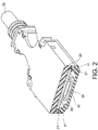
- FIG. 2 is a cross-sectional view of the photoelectric sensor 100 according to the first embodiment of the disclosure and illustrates a cross section taken along line A-A of FIG. 1 .
- FIG. 2 is a view illustrating an inside of the housing 30.
- the photoelectric sensor 100 includes a cover portion (protective portion 10 and side wall 11), a substrate 20, and a sealing member 25.
- the substrate 20 is positioned to be sandwiched between the protective portion 10 and the sealing member 25.
- a light receiving element 24 is mounted on the substrate 20.
- the cover portion includes the protective portion 10 and the side wall 11.
- the protective portion 10 is positioned to face the substrate 20.
- the side wall 11 extends from a peripheral edge of the protective portion 10 toward the substrate 20 side.
- the protective portion 10 and the side wall 11 may be integrally formed as the same member or may be formed as different members.
- the side wall 11 prevents the sealing member 25 from flowing into a hollow region provided between the substrate 20 and the protective portion 10.
- An end portion of the side wall 11 is recessed inside so that it is formed in an L-shape in a cross-sectional view.
- the light receiving element 24 such as a photodiode is mounted on the substrate 20.
- An end portion 21 of the substrate 20 is positioned to be in contact with a part of the L-shaped recess formed in the side wall 11.
- a hollow region is provided between the substrate 20 and the protective portion 10, and the light receiving element 24 or the like mounted on the substrate 20 is housed in the hollow region.
- a heat-shock to the light receiving element 24 can be alleviated and failure of the photoelectric sensor 100 can be prevented.
- arbitrary components such as a light receiving lens, an integrated circuit (IC) package, and the like may be mounted on the substrate 20.
- the sealing member 25 seals internal components such as the light receiving element 24 mounted on the substrate 20. Sealing with the sealing member 25 is performed by disposing the cover portion, the substrate 20, and the like in a sealing mold and then pouring a heated sealing member 25 into the sealing mold. By sealing with the sealing member 25, it is possible to protect the internal components from moisture, dust, or the like.
- the sealing member 25 may be, for example, a resin such as a hot-melt resin.
- FIG. 3 is an enlarged view of the side wall 11 and the end portion 21 of the substrate 20 in the cross section of the photoelectric sensor 100 according to the first embodiment of the disclosure.
- the side wall 11 includes a first portion 12 having a first width a and a second portion 13 having a second width b smaller than the first width a.
- the first portion 12 is positioned between the protective portion 10 and the second portion 13.
- the second portion 13 extends in a direction away from the protective portion 10 from a region on an outer side of an end surface 12a of the first portion 12.
- the end surface 12a of the first portion 12 and an inner wall 13a of the second portion 13 form an L-shaped recess in a cross-sectional view.
- the end portion 21 of the substrate 20 includes a front surface 21a and a side surface 21b.
- the surface 21a does not refer to the entire surface of the substrate 20, and refers to a peripheral edge portion in the surface region of the substrate 20.
- the surface 21a is in contact with the end surface 12a of the first portion 12.
- the side surface 21b is positioned to face the inner wall 13a of the second portion 13, and a gap is provided between the side surface 21b and the inner wall 13a.
- sealing by the sealing member 25 will be described.
- sealing with the sealing member 25 is performed by disposing the cover portion, the substrate 20, and the like in a sealing mold and then pouring a heated sealing member 25 into the sealing mold.
- the sealing member 25 enters the gap provided between the side surface 21b and the inner wall 13a.
- a direction in which the sealing member 25 flows is restricted only in a y direction (downward direction in FIG. 3 ) by the side surface 21b and the inner wall 13a. Therefore, the sealing member 25 does not move in an x direction along the surface 21a (the direction from the outside to the inside of the side wall 11), and the sealing member 25 does not flow into the hollow region from a space between the surface 21a and the end surface 12a.
- the sealing member 25 can be prevented from flowing into a space between the substrate 20 and the cover portion without bringing the entire region of the end surface of the side wall 11 into contact with the surface of the substrate 20, a component mounting region can be largely secured on the substrate 20. Therefore, large-sized components such as packaged electronic components can be mounted on the substrate 20. Also, since it is not necessary to bond the substrate 20 and the cover portion with an adhesive to prevent the sealing member 25 from entering the hollow region, a manufacturing efficiency of the photoelectric sensor 100 can be improved.
- a component mounting region can be largely secured on the substrate 20
- large IC packages, modules, or the like can be mounted on the substrate 20.
- an optical element such as the light receiving element 24 can be mounted on the substrate 20 in a packaged state, and the optical element can be protected from an external impact, humidity, heat, or the like.
- FIG. 4 is an enlarged view of an end portion of a substrate 22 in a cross section of a photoelectric sensor according to a second embodiment of the disclosure.
- the photoelectric sensor according to the second embodiment is different from the photoelectric sensor 100 according to the first embodiment in that a side surface 23b of the substrate 22 and an inner wall 13a of a second portion 13 are in contact with each other.
- the photoelectric sensor according to the present embodiment has the same configuration as the photoelectric sensor 100 according to the first embodiment.
- An end portion 23 of the substrate 22 has a surface 23a and the side surface 23b.
- the surface 23a does not refer to the entire surface of the substrate 22, and refers to a peripheral edge portion in the surface region of the substrate 22.
- the surface 23a is in contact with an end surface 12a of a first portion 12.
- the side surface 23b is in contact with the inner wall 13a of the second portion 13, and in this embodiment, they are in surface contact with each other.
- a contact area between the end portion 23 of the substrate 22 and a side wall 11 of the cover portion can be increased. Therefore, in a sealing process, it is possible to more reliably prevent a sealing member 25 from entering a hollow region from a space between the substrate 20 and the cover portion. Further, since the side surface 23b of the substrate 22 is in contact with the inner wall 13a of the second portion 13, positioning of the substrate 22 with respect to the cover portion can be accurately performed at the time of assembly.
- a photoelectric sensor 100 having at least any one of a light emitting unit that emits light and a light receiving unit that detects light includes a substrate 20 on which at least any one of the light emitting unit and the light receiving unit is mounted, and a cover portion having a protective portion 10 facing the substrate 20 and configured to protect the substrate 20, and a side wall 1 1 extending from a peripheral edge of the protective portion 10 toward the substrate 20 side, in which the side wall 11 of the cover portion includes a first portion 12 formed in a first width and a second portion 13 formed in a second width smaller than the first width, the first portion 12 is positioned between the protective portion 10 and the second portion 13, a surface 21a in an end portion 21 of the substrate 20 is in contact with the first portion 12, and a side surface 21b in the end portion 21 of the substrate 20 faces the second portion 13.
Landscapes
- Physics & Mathematics (AREA)
- Engineering & Computer Science (AREA)
- General Physics & Mathematics (AREA)
- Remote Sensing (AREA)
- Electromagnetism (AREA)
- Computer Networks & Wireless Communication (AREA)
- Radar, Positioning & Navigation (AREA)
- Geophysics (AREA)
- General Life Sciences & Earth Sciences (AREA)
- Life Sciences & Earth Sciences (AREA)
- Switches Operated By Changes In Physical Conditions (AREA)
- Photometry And Measurement Of Optical Pulse Characteristics (AREA)
- Microelectronics & Electronic Packaging (AREA)
Abstract
Description
- The disclosure relates to a photoelectric sensor.
- Conventionally, a photoelectric sensor is used to detect the presence or absence of an object in a detection region (for example, Patent Document 1 or the like). In photoelectric sensors, there is a transmission-type sensor having a light emitting unit for emitting light and a light receiving unit for detecting light which are housed in separate housings and configured such that light emitted from one photoelectric sensor is received by the other photoelectric sensor. When an object is present between the light emitting unit and the light receiving unit, light is blocked and an amount of light received by the light receiving unit decreases. The transmission-type sensor detects the presence or absence of an object by measuring the decrement. In photoelectric sensors, there is also a reflection-type sensor having a light emitting unit and a light receiving unit which are housed in an integrated housing and configured to detect the presence or absence of an object or the like by reflecting light on the object and measuring the reflected light.
- The light emitting unit and the light receiving unit are each configured by optical elements such as a light emitting diode or a photodiode, and are mounted on a substrate inside the housing. In order to seal these optical elements, after disposing the substrate inside the housing, a sealing member such as a resin may be filled into the inside of the housing. However, when the sealing member adheres to the optical elements, since an amount of light emitted and received by an optical element decreases, there is a likelihood that object detection will not be accurately performed. Therefore, as illustrated in
FIG. 5 , a cover constituted by aprotective portion 41 and aside wall 42 is made to cover asubstrate 40 to prevent a sealingmember 44 from adhering to anoptical element 45. In a sealing process, anend surface 43 of theside wall 42 is adhered to thesubstrate 40 with an adhesive so that the sealingmember 44 does not flow from a space between thesubstrate 40 and theside wall 42. - [Patent Document 1] Japanese Laid-open No.
2014-107698 - However, in the above-described method of adhering the entire region of the
end surface 43 of theside wall 42 to thesubstrate 40, it is difficult to secure a large mounting region on the substrate. Therefore, it is difficult to mount large-size packaged components or the like on the substrate. - Accordingly, it is an objective of the disclosure to provide a photoelectric sensor in which a large mounting region can be secured on a substrate.
- A photoelectric sensor according to one aspect of the disclosure is a photoelectric sensor having at least any one of a light emitting unit that emits light and a light receiving unit that detects light, and the photoelectric sensor includes a substrate on which at least any one of the light emitting unit and the light receiving unit is mounted, and a cover portion including a protective portion facing the substrate and configured to protect the substrate and a side wall extending from a peripheral edge of the protective portion toward the substrate side, in which the side wall of the cover portion includes a first portion formed in a first width, and a second portion formed in a second width smaller than the first width, the first portion is positioned between the protective portion and the second portion, a surface in an end portion of the substrate is in contact with the first portion, and a side surface in the end portion of the substrate faces the second portion.
- According to this aspect, since a sealing member can be prevented from flowing into a space between the substrate and the cover portion without bringing the entire region of the end surface of the side wall into contact with the surface of the substrate, a component mounting region can be largely secured on the substrate. Therefore, large-size components such as packaged electronic components can be mounted on the substrate.
- In the above aspect, the side surface in the end portion of the substrate may be in contact with the side wall.
- According to this aspect, a contact area between the end portion of the substrate and the side wall of the cover portion can be increased, and it is possible to more reliably prevent the sealing member from entering a hollow region provided between the substrate and the cover portion. Further, since the side surface of the substrate is in contact with the inner wall of the second portion, positioning of the substrate with respect to the cover portion can be accurately performed at the time of assembly.
- In the above aspect, an integrated circuit (IC) package may be mounted on the substrate.
- According to this aspect, components such as optical elements included in the photoelectric sensor are mounted on the substrate in a packaged state. Therefore, the optical elements can be protected from an external impact, humidity, heat, or the like.
- In the above aspect, a lens may be formed in the protective portion.
- According to this aspect, since the lens is formed in the protective portion, there is no need to secure a region for mounting a lens on the substrate. Therefore, a space for mounting components other than lens can be largely secured, and a larger component can be mounted on the substrate.
- According to the disclosure, it is possible to provide a photoelectric sensor in which a large mounting region can be secured on a substrate.
-
-
FIG. 1 is a perspective view of a photoelectric sensor according to a first embodiment of the disclosure. -
FIG. 2 is a cross-sectional view of the photoelectric sensor according to the first embodiment of the disclosure. -
FIG. 3 is an enlarged cross-sectional view of the photoelectric sensor according to the first embodiment of the disclosure. -
FIG. 4 is an enlarged cross-sectional view of a photoelectric sensor according to a second embodiment of the disclosure. -
FIG. 5 is a cross-sectional view of a conventional photoelectric sensor. - Embodiments of the disclosure will be described with reference to the accompanying drawings. In each of the drawings, the same reference signs are given to the same or similar components.
-
FIG. 1 is a perspective view of aphotoelectric sensor 100 according to a first embodiment of the disclosure. A photoelectric sensor detects the presence or absence of an object in a detection region, a surface state of an object, or the like using light. There are a plurality of detection methods using photoelectric sensors. For example, two photoelectric sensors may be prepared, one photoelectric sensor may be used as a light emitter for emitting light, and the other photoelectric sensor may be used as a light receiver for detecting light. When an object is present between the light emitter and the light receiver, an amount of light received by the light receiver decreases. The photoelectric sensor measures the decrement to detect the presence or absence of an object. The photoelectric sensor used in this detection method is called a transmission-type sensor. - Further, as another detection method, there is also a method of performing detection using a photoelectric sensor in which a light emitter and a light receiver are integrated. Light from a photoelectric sensor is emitted toward a reflection plate, a detection object, or the like, and the same photoelectric sensor receives and measures the reflected light, thereby detecting the presence or absence of an object. Such a photoelectric sensor which functions as both a light emitter and a light receiver is called a reflection-type sensor.
- With reference to
FIG. 1 , a configuration of thephotoelectric sensor 100 will be described. In the present specification, thephotoelectric sensor 100 operating as a light receiver among the photoelectric sensors of transmission-type will be described as an example, but photoelectric sensors to which the disclosure is applied may be a photoelectric sensor operating as a light emitter or a photoelectric sensor of a reflection-type. Thephotoelectric sensor 100 includes ahousing 30, aprotective portion 10, awindow 38, and acable 39. Further, a light receivinglens 15 is formed in theprotective portion 10. - The
housing 30 protects various components such as a light receiving element contained in thephotoelectric sensor 100 from an impact or contamination from the outside. Thehousing 30 is made of a metal or a resin, for example. Thehousing 30 has afront surface 31, aback surface 32, aside surface 33, aside surface 34, atop surface 35, and abottom surface 36. A surface on which light from a detection region is incident is thefront surface 31, and theback surface 32 is positioned to face thefront surface 31 with the inside of thehousing 30 interposed therebetween. Further, theside surface 33 and theside surface 34 are positioned to face each other with the inside of thehousing 30 interposed therebetween. Similarly, thetop surface 35 and thebottom surface 36 are also positioned to face each other with the inside of thehousing 30 interposed therebetween. - A
mounting hole 37 is provided in thehousing 30, and a screw or the like can be inserted into themounting hole 37 to fix thephotoelectric sensor 100 to a wall, a floor surface, a ceiling, or the like. A distance between thefront surface 31 and theback surface 32 is configured to be smaller than a distance between theside surface 33 and theside surface 34 so that a thickness of thephotoelectric sensor 100 in a side view becomes small. Therefore, even when a space for mounting thephotoelectric sensor 100 is narrow, thephotoelectric sensor 100 can easily be installed. Further, a distance between thefront surface 31 and theback surface 32 is not necessarily smaller than a distance between theside surface 33 and theside surface 34. - A part or all of a light receiving unit is housed inside the
housing 30. The light receiving unit is a portion that detects light incident from a detection region, and includes a light receiving element and thelight receiving lens 15. The light receiving element may be, for example, a photodiode or a position detecting element. Thelight receiving lens 15 is a lens that causes light incident from the detection region to form an image on the light receiving element. Thelight receiving lens 15 may be housed inside thehousing 30, or may be formed in theprotective portion 10 as illustrated inFIG. 1 while being partially exposed to the outside of thehousing 30. When a lens is formed in theprotective portion 10 as in this example, there is no need to secure a region for mounting a lens on the substrate. Therefore, a mounting space for components other than the lens can be largely secured, and a larger component can be mounted on the substrate. - Further, a photoelectric sensor operating as a light emitter includes a light emitting unit for emitting light, and the light emitting unit is constituted by a light emitting element, a light emitting lens, and the like. The light emitting element may be, for example, a light emitting diode (LED) or the like. The light emitting lens may be housed inside the housing, or may be formed integrally with the protective portion while being partially exposed to the outside of the housing as in the
photoelectric sensor 100 illustrated inFIG. 1 . - The
protective portion 10 protects components such as the light receiving element housed in thephotoelectric sensor 100. Since theprotective portion 10 is disposed on a surface receiving light incident from a detection region, theprotective portion 10 is formed of a material that transmits light so that the light receiving element positioned inside thephotoelectric sensor 100 can detect the light. For example, theprotective portion 10 may be formed of a resin or the like. Further, the entireprotective portion 10 need not be formed of a material that transmits light and, for example, only thelight receiving lens 15 may be formed of a member that transmits light so that the light receiving element detects light through thelight receiving lens 15. - The
window 38 protects an indicator (not illustrated) provided on an upper portion of thephotoelectric sensor 100 from an impact or contamination. The indicator displays a power supply status, detection status, or the like of thephotoelectric sensor 100. The indicator may be configured by light emitting elements such as a light emitting diode, for example. The indicator may be lit when a power supply of thephotoelectric sensor 100 is turned on or when thephotoelectric sensor 100 detects an object. Further, the indicator may be lit using light of different colors according to types of objects detected by thephotoelectric sensor 100. - The
cable 39 transmits electric power supplied from a power supply to thephotoelectric sensor 100. Also, thecable 39 can connect thephotoelectric sensor 100 to an amplifier unit including an amplifier unit, a control unit, or the like to transmit detection results obtained by thephotoelectric sensor 100. In the present example, thecable 39 is connected to thebottom surface 36 of thephotoelectric sensor 100, but the connecting position is not necessarily thebottom surface 36 and it may be connected to theside surface 33, theside surface 34, thetop surface 35 or the like. At least any one of the power supply and the amplifier unit may be incorporated in thephotoelectric sensor 100. -
FIG. 2 is a cross-sectional view of thephotoelectric sensor 100 according to the first embodiment of the disclosure and illustrates a cross section taken along line A-A ofFIG. 1 . With reference toFIG. 2 , an internal configuration of thephotoelectric sensor 100 according to the present embodiment will be described.FIG. 2 is a view illustrating an inside of thehousing 30. - The
photoelectric sensor 100 includes a cover portion (protective portion 10 and side wall 11), asubstrate 20, and a sealingmember 25. Thesubstrate 20 is positioned to be sandwiched between theprotective portion 10 and the sealingmember 25. On thesubstrate 20, alight receiving element 24 is mounted. - The cover portion includes the
protective portion 10 and theside wall 11. Theprotective portion 10 is positioned to face thesubstrate 20. Theside wall 11 extends from a peripheral edge of theprotective portion 10 toward thesubstrate 20 side. Theprotective portion 10 and theside wall 11 may be integrally formed as the same member or may be formed as different members. - In a sealing process, the
side wall 11 prevents the sealingmember 25 from flowing into a hollow region provided between thesubstrate 20 and theprotective portion 10. An end portion of theside wall 11 is recessed inside so that it is formed in an L-shape in a cross-sectional view. - The
light receiving element 24 such as a photodiode is mounted on thesubstrate 20. Anend portion 21 of thesubstrate 20 is positioned to be in contact with a part of the L-shaped recess formed in theside wall 11. A hollow region is provided between thesubstrate 20 and theprotective portion 10, and thelight receiving element 24 or the like mounted on thesubstrate 20 is housed in the hollow region. By housing thelight receiving element 24 in the hollow region, a heat-shock to thelight receiving element 24 can be alleviated and failure of thephotoelectric sensor 100 can be prevented. Further, arbitrary components such as a light receiving lens, an integrated circuit (IC) package, and the like may be mounted on thesubstrate 20. - The sealing
member 25 seals internal components such as thelight receiving element 24 mounted on thesubstrate 20. Sealing with the sealingmember 25 is performed by disposing the cover portion, thesubstrate 20, and the like in a sealing mold and then pouring aheated sealing member 25 into the sealing mold. By sealing with the sealingmember 25, it is possible to protect the internal components from moisture, dust, or the like. The sealingmember 25 may be, for example, a resin such as a hot-melt resin. -
FIG. 3 is an enlarged view of theside wall 11 and theend portion 21 of thesubstrate 20 in the cross section of thephotoelectric sensor 100 according to the first embodiment of the disclosure. - The
side wall 11 includes afirst portion 12 having a first width a and asecond portion 13 having a second width b smaller than the first width a. Thefirst portion 12 is positioned between theprotective portion 10 and thesecond portion 13. Thesecond portion 13 extends in a direction away from theprotective portion 10 from a region on an outer side of anend surface 12a of thefirst portion 12. Theend surface 12a of thefirst portion 12 and aninner wall 13a of thesecond portion 13 form an L-shaped recess in a cross-sectional view. - A positional relationship between the
end portion 21 of thesubstrate 20 and the L-shaped recess will be described. Theend portion 21 of thesubstrate 20 includes afront surface 21a and aside surface 21b. Here, thesurface 21a does not refer to the entire surface of thesubstrate 20, and refers to a peripheral edge portion in the surface region of thesubstrate 20. When thesubstrate 20 and the cover portion are combined, thesurface 21a is in contact with theend surface 12a of thefirst portion 12. Further, theside surface 21b is positioned to face theinner wall 13a of thesecond portion 13, and a gap is provided between theside surface 21b and theinner wall 13a. - Next, sealing by the sealing
member 25 will be described. As described above, sealing with the sealingmember 25 is performed by disposing the cover portion, thesubstrate 20, and the like in a sealing mold and then pouring aheated sealing member 25 into the sealing mold. When the sealingmember 25 is poured into the sealing mold, the sealingmember 25 enters the gap provided between theside surface 21b and theinner wall 13a. At this time, a direction in which the sealingmember 25 flows is restricted only in a y direction (downward direction inFIG. 3 ) by theside surface 21b and theinner wall 13a. Therefore, the sealingmember 25 does not move in an x direction along thesurface 21a (the direction from the outside to the inside of the side wall 11), and the sealingmember 25 does not flow into the hollow region from a space between thesurface 21a and theend surface 12a. - According to the
photoelectric sensor 100 of the present embodiment, since the sealingmember 25 can be prevented from flowing into a space between thesubstrate 20 and the cover portion without bringing the entire region of the end surface of theside wall 11 into contact with the surface of thesubstrate 20, a component mounting region can be largely secured on thesubstrate 20. Therefore, large-sized components such as packaged electronic components can be mounted on thesubstrate 20. Also, since it is not necessary to bond thesubstrate 20 and the cover portion with an adhesive to prevent the sealingmember 25 from entering the hollow region, a manufacturing efficiency of thephotoelectric sensor 100 can be improved. - Further, according to the
photoelectric sensor 100 of the present embodiment, since a component mounting region can be largely secured on thesubstrate 20, large IC packages, modules, or the like can be mounted on thesubstrate 20. For example, an optical element such as thelight receiving element 24 can be mounted on thesubstrate 20 in a packaged state, and the optical element can be protected from an external impact, humidity, heat, or the like. -
FIG. 4 is an enlarged view of an end portion of asubstrate 22 in a cross section of a photoelectric sensor according to a second embodiment of the disclosure. The photoelectric sensor according to the second embodiment is different from thephotoelectric sensor 100 according to the first embodiment in that aside surface 23b of thesubstrate 22 and aninner wall 13a of asecond portion 13 are in contact with each other. Regarding other configurations, the photoelectric sensor according to the present embodiment has the same configuration as thephotoelectric sensor 100 according to the first embodiment. - An
end portion 23 of thesubstrate 22 has asurface 23a and theside surface 23b. Here, as in thesurface 21a according to the first embodiment, thesurface 23a does not refer to the entire surface of thesubstrate 22, and refers to a peripheral edge portion in the surface region of thesubstrate 22. When thesubstrate 22 and a cover portion are combined, thesurface 23a is in contact with anend surface 12a of afirst portion 12. Further, theside surface 23b is in contact with theinner wall 13a of thesecond portion 13, and in this embodiment, they are in surface contact with each other. - According to this aspect, a contact area between the
end portion 23 of thesubstrate 22 and aside wall 11 of the cover portion can be increased. Therefore, in a sealing process, it is possible to more reliably prevent a sealingmember 25 from entering a hollow region from a space between thesubstrate 20 and the cover portion. Further, since theside surface 23b of thesubstrate 22 is in contact with theinner wall 13a of thesecond portion 13, positioning of thesubstrate 22 with respect to the cover portion can be accurately performed at the time of assembly. - The embodiments described above are for facilitating understanding of the disclosure and are not intended to limit the disclosure. The elements and, an arrangement, a material, conditions, a shape, a size, and the like thereof of the embodiments are not limited to those exemplified and can be appropriately changed. Further, configurations illustrated in the different embodiments can be partially substituted or combined.
- A
photoelectric sensor 100 having at least any one of a light emitting unit that emits light and a light receiving unit that detects light includes asubstrate 20 on which at least any one of the light emitting unit and the light receiving unit is mounted, and a cover portion having aprotective portion 10 facing thesubstrate 20 and configured to protect thesubstrate 20, and a side wall 1 1 extending from a peripheral edge of theprotective portion 10 toward thesubstrate 20 side, in which theside wall 11 of the cover portion includes afirst portion 12 formed in a first width and asecond portion 13 formed in a second width smaller than the first width, thefirst portion 12 is positioned between theprotective portion 10 and thesecond portion 13, asurface 21a in anend portion 21 of thesubstrate 20 is in contact with thefirst portion 12, and aside surface 21b in theend portion 21 of thesubstrate 20 faces thesecond portion 13. -
- 10 Protective portion
- 11 Side wall
- 12 First portion
- 12a End surface
- 13 Second portion
- 13a Inner wall
- 15 Light receiving lens
- 20 Substrate
- 21 End portion
- 21a Surface
- 21b Side surface
- 22 Substrate
- 23 End portion
- 23a Surface
- 23b Side surface
- 24 Light receiving element
- 25 Sealing member
- 30 Housing
- 31 Front surface
- 32 Back surface
- 33 Side surface
- 34 Side surface
- 35 Top surface
- 36 Bottom surface
- 37 Mounting hole
- 38 Window
- 39 Cable
- 40 Substrate
- 41 Protective portion
- 42 Side wall
- 43 End surface
- 44 Sealing member
- 45 Optical element
- 100 Photoelectric sensor
Claims (4)
- A photoelectric sensor (100) having at least any one of a light emitting unit that emits light and a light receiving unit that detects light, the photoelectric sensor (100) characterized in that comprising:a substrate (20) on which at least any one of the light emitting unit and the light receiving unit is mounted; anda cover portion including:a protective portion (10) facing the substrate (20) and configured to protect the substrate (20); anda side wall (11) extending from a peripheral edge of the protective portion (10) toward the substrate (20) side, whereinthe side wall (11) of the cover portion includes:a first portion (12) formed in a first width; anda second portion (13) formed in a second width smaller than the first width,the first portion (12) is positioned between the protective portion (10) and the second portion (13),a surface (21a) in an end portion (21) of the substrate (20) is in contact with the first portion (12), anda side surface (21b) in the end portion (21) of the substrate (20) faces the second portion (13).
- The photoelectric sensor (100) according to claim 1, wherein the side surface (21b) in the end portion (21) of the substrate (20) is in contact with the side wall (11).
- The photoelectric sensor (100) according to claim 1 or 2, wherein an integrated circuit package is mounted on the substrate (20).
- The photoelectric sensor (100) according to any one of claims 1 to 3, wherein a lens (15) is formed in the protective portion (10).
Applications Claiming Priority (1)
| Application Number | Priority Date | Filing Date | Title |
|---|---|---|---|
| JP2018048030A JP6995288B2 (en) | 2018-03-15 | 2018-03-15 | Photoelectric sensor |
Publications (1)
| Publication Number | Publication Date |
|---|---|
| EP3540472A1 true EP3540472A1 (en) | 2019-09-18 |
Family
ID=65440767
Family Applications (1)
| Application Number | Title | Priority Date | Filing Date |
|---|---|---|---|
| EP19156569.6A Withdrawn EP3540472A1 (en) | 2018-03-15 | 2019-02-12 | Photoelectric sensor |
Country Status (4)
| Country | Link |
|---|---|
| US (1) | US20190288153A1 (en) |
| EP (1) | EP3540472A1 (en) |
| JP (1) | JP6995288B2 (en) |
| CN (1) | CN110274616A (en) |
Citations (7)
| Publication number | Priority date | Publication date | Assignee | Title |
|---|---|---|---|---|
| US20030071342A1 (en) * | 2001-02-28 | 2003-04-17 | Fujitsu Limited | Semiconductor device and method for making the same |
| US20050184219A1 (en) * | 2004-02-23 | 2005-08-25 | Kirby Kyle K. | Packaged microelectronic imagers and methods of packaging microelectronic imagers |
| JP2012122858A (en) * | 2010-12-08 | 2012-06-28 | Panasonic Corp | Reflection-type photoelectric sensor and manufacturing method thereof |
| US20130265590A1 (en) * | 2010-10-04 | 2013-10-10 | Robert Bosch Gmbh | Optical Shielding Device for Separating Optical Paths |
| JP2014107698A (en) | 2012-11-27 | 2014-06-09 | Keyence Corp | Photoelectric sensor |
| US20170052277A1 (en) * | 2015-08-21 | 2017-02-23 | Stmicroelectronics Pte Ltd | Molded range and proximity sensor with optical resin lens |
| US20170123101A1 (en) * | 2015-11-02 | 2017-05-04 | Stmicroelectronics Pte Ltd | Proximity sensor, electronic apparatus and method for manufacturing proximity sensor |
Family Cites Families (9)
| Publication number | Priority date | Publication date | Assignee | Title |
|---|---|---|---|---|
| US5078497A (en) * | 1989-08-25 | 1992-01-07 | Xerox Corporation | Densitometer for a liquid developer material |
| JP3868035B2 (en) * | 1996-07-31 | 2007-01-17 | オリンパス株式会社 | Ranging device |
| JP2009097872A (en) * | 2007-10-12 | 2009-05-07 | Sharp Corp | Optical distance sensor, object detection device, cleaning toilet seat, and method of manufacturing optical distance sensor |
| JP5178393B2 (en) * | 2008-08-20 | 2013-04-10 | シャープ株式会社 | Optical distance measuring sensor and electronic device |
| JP2013206836A (en) * | 2012-03-29 | 2013-10-07 | Azbil Corp | Reflection type photoelectric sensor |
| JP6097020B2 (en) * | 2012-06-04 | 2017-03-15 | 株式会社キーエンス | Optical sensor |
| JP5964687B2 (en) * | 2012-08-02 | 2016-08-03 | 株式会社キーエンス | Optical sensor |
| FR3001545B1 (en) * | 2013-01-31 | 2015-03-20 | Continental Automotive France | INFRARED OPTICAL SENSOR INTEGRATING A TRANSMISSION MEASURING CELL |
| TW201837427A (en) * | 2017-04-11 | 2018-10-16 | 達帕有限公司 | Composite optic sensor having natural barrier formed by ambient light sensor die in which a vertical cavity surface emitting laser, an ambient light sensor die, and a proximity sensor are arranged linearly with a raised height that is sufficient to serve as a natural barrier |
-
2018
- 2018-03-15 JP JP2018048030A patent/JP6995288B2/en active Active
-
2019
- 2019-02-12 CN CN201910110700.9A patent/CN110274616A/en active Pending
- 2019-02-12 EP EP19156569.6A patent/EP3540472A1/en not_active Withdrawn
- 2019-02-15 US US16/276,624 patent/US20190288153A1/en not_active Abandoned
Patent Citations (7)
| Publication number | Priority date | Publication date | Assignee | Title |
|---|---|---|---|---|
| US20030071342A1 (en) * | 2001-02-28 | 2003-04-17 | Fujitsu Limited | Semiconductor device and method for making the same |
| US20050184219A1 (en) * | 2004-02-23 | 2005-08-25 | Kirby Kyle K. | Packaged microelectronic imagers and methods of packaging microelectronic imagers |
| US20130265590A1 (en) * | 2010-10-04 | 2013-10-10 | Robert Bosch Gmbh | Optical Shielding Device for Separating Optical Paths |
| JP2012122858A (en) * | 2010-12-08 | 2012-06-28 | Panasonic Corp | Reflection-type photoelectric sensor and manufacturing method thereof |
| JP2014107698A (en) | 2012-11-27 | 2014-06-09 | Keyence Corp | Photoelectric sensor |
| US20170052277A1 (en) * | 2015-08-21 | 2017-02-23 | Stmicroelectronics Pte Ltd | Molded range and proximity sensor with optical resin lens |
| US20170123101A1 (en) * | 2015-11-02 | 2017-05-04 | Stmicroelectronics Pte Ltd | Proximity sensor, electronic apparatus and method for manufacturing proximity sensor |
Also Published As
| Publication number | Publication date |
|---|---|
| US20190288153A1 (en) | 2019-09-19 |
| CN110274616A (en) | 2019-09-24 |
| JP6995288B2 (en) | 2022-01-14 |
| JP2019160687A (en) | 2019-09-19 |
Similar Documents
| Publication | Publication Date | Title |
|---|---|---|
| US11002596B2 (en) | Photoelectric sensor and manufacturing method thereof | |
| US10466079B2 (en) | Sensor device | |
| JP5711009B2 (en) | Liquid crystal display | |
| US12292504B2 (en) | Displacement sensor | |
| JP2015158831A (en) | Coordinate input device and image display device | |
| WO2020175676A1 (en) | Photoelectric sensor and method for manufacturing same | |
| TWI498585B (en) | Optical proximity sensor and assembling method thereof | |
| TW202103335A (en) | Optical device and method of manufacturing the same | |
| EP3540389A1 (en) | Photoelectric sensor | |
| EP3540472A1 (en) | Photoelectric sensor | |
| JP6097020B2 (en) | Optical sensor | |
| US10795148B2 (en) | Micromechanical component, micromirror-based laser system, and method for monitoring a micromirror-based laser system comprising dual sensor diodes for sensing temperature and light intensity | |
| EP3540489A1 (en) | Small photoelectric sensor | |
| JP4616676B2 (en) | Color toner adhesion measuring device | |
| KR20190108527A (en) | Optical sensor package | |
| JP4121033B2 (en) | Heat sensor | |
| US20130208465A1 (en) | Laser light source module and method of manufacturing laser light source module | |
| US11832499B2 (en) | Sensor | |
| GB2536206A (en) | System and method for the detection of light transmission and light reflection | |
| JP2004257857A (en) | Photoelectric sensor | |
| JP2006078376A (en) | Optical displacement sensor | |
| JP2007188541A (en) | Heat sensor | |
| JP2014150099A (en) | Package for housing optical element, optical filter device, optical module and electronic apparatus | |
| CN110007500A (en) | Display device | |
| JP2013072844A (en) | Fluid reaction detection module and fluid reaction detection system |
Legal Events
| Date | Code | Title | Description |
|---|---|---|---|
| PUAI | Public reference made under article 153(3) epc to a published international application that has entered the european phase |
Free format text: ORIGINAL CODE: 0009012 |
|
| STAA | Information on the status of an ep patent application or granted ep patent |
Free format text: STATUS: REQUEST FOR EXAMINATION WAS MADE |
|
| 17P | Request for examination filed |
Effective date: 20190212 |
|
| AK | Designated contracting states |
Kind code of ref document: A1 Designated state(s): AL AT BE BG CH CY CZ DE DK EE ES FI FR GB GR HR HU IE IS IT LI LT LU LV MC MK MT NL NO PL PT RO RS SE SI SK SM TR |
|
| AX | Request for extension of the european patent |
Extension state: BA ME |
|
| RBV | Designated contracting states (corrected) |
Designated state(s): AL AT BE BG CH CY CZ DE DK EE ES FI FR GB GR HR HU IE IS IT LI LT LU LV MC MK MT NL NO PL PT RO RS SE SI SK SM TR |
|
| STAA | Information on the status of an ep patent application or granted ep patent |
Free format text: STATUS: EXAMINATION IS IN PROGRESS |
|
| 17Q | First examination report despatched |
Effective date: 20200820 |
|
| STAA | Information on the status of an ep patent application or granted ep patent |
Free format text: STATUS: THE APPLICATION HAS BEEN WITHDRAWN |
|
| 18W | Application withdrawn |
Effective date: 20200915 |